
 Open Access Article
 This Open Access Article is licensed under a Creative Commons Attribution-Non Commercial 3.0 Unported Licence
Bimodal alteration of cognitive accuracy for spintronic artificial neural networks
Anuj
Kumar
a,
Debasis
Das
b,
Dennis J. X.
Lin
c,
Lisen
Huang
c,
Sherry L. K.
Yap
c,
Hang Khume
Tan
c,
Royston J. J.
Lim
 c,
Hui Ru
Tan
c,
Yeow Teck
Toh
c,
Sze Ter
Lim
c,
Xuanyao
Fong
*b and
Pin
Ho
*c
c,
Hui Ru
Tan
c,
Yeow Teck
Toh
c,
Sze Ter
Lim
c,
Xuanyao
Fong
*b and
Pin
Ho
*c
aPhysics Department, National University of Singapore, Singapore, 117551, Singapore
bElectrical and Computer Engineering Department, National University of Singapore, Singapore, 117583, Singapore. E-mail: kelvin.xy.fong@nus.edu.sg
cInstitute of Materials Research and Engineering (IMRE), Agency for Science, Technology and Research (A*STAR), 2 Fusionopolis Way, Singapore, 138634, Singapore. E-mail: hopin@imre.a-star.edu.sg
First published on 2nd July 2024
Abstract
Spintronics-based artificial neural networks (ANNs) exhibiting nonvolatile, fast, and energy-efficient computing capabilities are promising neuromorphic hardware for performing complex cognitive tasks of artificial intelligence and machine learning. Early experimental efforts focused on multistate device concepts to enhance synaptic weight precisions, albeit compromising on cognitive accuracy due to their low magnetoresistance. Here, we propose a hybrid approach based on the tuning of tunnel magnetoresistance (TMR) and the number of states in the compound magnetic tunnel junctions (MTJs) to improve the cognitive performance of an all-spin ANN. A TMR variation of 33–78% is controlled by the free layer (FL) thickness wedge (1.6–2.6 nm) across the wafer. Meanwhile, the number of resistance states in the compound MTJ is manipulated by varying the number of constituent MTJ cells (n = 1–3), generating n + 1 states with a TMR difference between consecutive states of at least 21%. Using MNIST handwritten digit and fashion object databases, the test accuracy of the compound MTJ ANN is observed to increase with the number of intermediate states for a fixed FL thickness or TMR. Meanwhile, the test accuracy for a 1-cell MTJ increases linearly by 8.3% and 7.4% for handwritten digits and fashion objects, respectively, with increasing TMR. Interestingly, a multifarious TMR dependence of test accuracy is observed with the increasing synaptic complexity in the 2- and 3-cell MTJs. By leveraging on the bimodal tuning of multilevel and TMR, we establish viable paths for enhancing the cognitive performance of spintronic ANN for in-memory and neuromorphic computing.
New conceptsAchieving high cognitive accuracy in digit recognition and pattern detection tasks is a compelling attribute for high-performance spintronics-based artificial neural networks (ANNs). While earlier experimental efforts focused on developing multistate devices to mimic spin synapses of variable synaptic weights, such device concepts are mainly based on domain wall motion and vertically stacked MTJ which suffer from low magnetoresistance readout, and hence, poor synaptic resolution and higher recognition errors. Meanwhile, improvement in recognition accuracy through magnetoresistance modulation is posited in simulation, yet plausible experimental approaches are starkly absent. In this work, we introduce a novel bimodal experimental route to improve cognitive accuracy by tuning the number of states and tunneling magnetoresistance of the ANN constructed over a CMOS-compatible design of compound spin–orbit torque magnetic tunnel junctions (SOT-MTJs). This is achieved by the concomitant implementation of a network of multiple SOT-MTJ on a shared write channel and a free layer thickness wedge. Remarkably, we show 3-cell compound MTJ with TMR between states, which is 7-fold higher than reported state-of-the-art, and enhanced recognition accuracies when coupled with optimal free layer thickness. Our bimodal design provides a path to realize enhanced cognitive performance in spintronics ANN for in-memory and neuromorphic computing. |
A. Introduction
Neuromorphic computing, based on the brain-inspired framework of hosting massive interconnected artificial neurons and synapses as memory and processing units, can overcome the inevitable limitations of Von-Neuman architectures in performing computationally intensive tasks for artificial intelligence and big data.1–4 Nonvolatile neuromorphic concepts built upon resistive,5,6 phase change,7 and ferroelectric8,9 memristors typically require high energy (0.1–10 pJ) and long write time (10–100 ns) for switching, and display average endurance (106–1012 cycles) for practical and efficient computing applications.1 On the other hand, spin-based neuromorphic hardware utilizing the spin–orbit torque (SOT) mechanism for electrical switching is expected to offer energy efficiency (∼0.1 pJ), fast write (<10 ns) and read time (30 ns), and high endurance (1015 cycles), enabling scalable sustainable computing.10 In this light, the commercialized industry-compatible SOT-magnetic tunnel junctions (MTJs) – consisting of an insulating barrier sandwiched between the heavy metal/ferromagnetic free (FL) and reference layers, are the ideal building block for neurons and synapses, wherein the latter is mimicked by a multistate MTJ.11The functional performance of such spintronic neuromorphic devices is benchmarked to vital parameters such as their learning and testing accuracies in performing cognitive tasks of digit recognition and pattern detection.11,12 Numerous concepts have been proposed for accuracy improvements, including (i) the reduction of device energy barrier in enabling faster fluctuation speed for improved probabilistic behavior,13,14 (ii) the enhancement of magnetoresistance values to amplify the distinction between synaptic states,15 and (iii) the increase in the number of conductance states16–20 to strengthen synaptic weight precision. The first option of reducing the switching energy barrier introduces undesirable thermal instability and device reliability issues, as well as a higher recognition error rate due to its sensitivity to structural defects and process-related size variation.21 Notably, clubbing multistate synapses with a magnetoresistance-enhancing mechanism will be a promising means of concomitantly elevating the synaptic precision and resolution of artificial synapses for cognitive tasks. Yet, experimental efforts have largely been restricted to singly tuning the multistate functionality of synaptic devices built upon domain wall motion,22–24 and vertically stacked MTJ,17–19 albeit with low multistate magnetoresistance readout between two consecutive resistance states of <3%. Meanwhile, the notion of magnetoresistance modulation for enhanced accuracies is limited to simulations, without proposals of feasible routes for practical implementation. In this light, it is compelling to establish practical approaches to modulate the synaptic precision and resolution and elucidate their interplaying effects on the synaptic performance.
In this work, we adopt a bimodal approach of tuning multistate and magnetoresistance, by introducing compound MTJ with a varying number of SOT-MTJ cells (n = 1–3) and free layer thickness wedge of 1.6–2.6 nm, to modulate the digit and object recognition performance of our spintronic artificial neural network (ANN) (Fig. 1). We show that the CMOS-compatible compound MTJ design will enable thermally stable and well-distinguished multistate with large tunneling magnetoresistance (TMR) ratio between states. Further, the variation in the FL thickness enables more than 2-fold enhancement in TMR. By varying the number of states and TMR, we demonstrate enhanced test accuracies of the compound MTJ-based ANN in performing MNIST handwritten digit and fashion object recognition tasks. These results underscore that a high TMR multistate synapse is a feasible solution for enhanced performance of spin-based ANN in executing cognitive tasks.
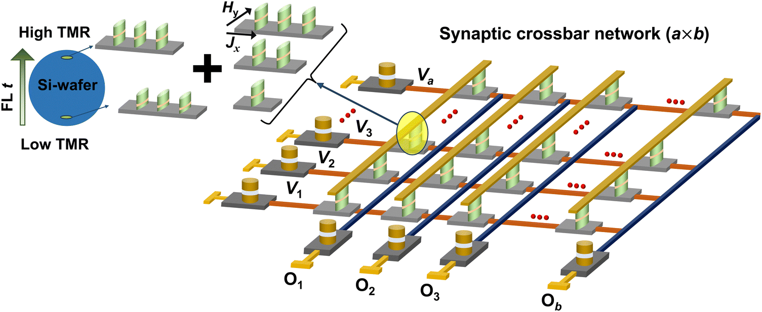 | ||
| Fig. 1 Spin-based artificial neural network (ANN). The spin–orbit torque magnetic tunnel junction (SOT-MTJ)-based crossbar array of artificial synapses connecting the two layers of neurons (input: a, output: b). An experimental bimodal approach of tuning free layer (FL) thickness (t) and the number of MTJ cells (circled, left inset) is utilized to improve the ANN cognitive performance. The FL thickness is controlled by the wedge (t: 1.6–2.6 nm) along the whole wafer, while t is uniform for all constituent MTJs across the compound MTJ. The synapses can be implemented using the compound SOT-MTJ device concept which incorporates 1, 2, and 3-cell MTJs without altering the prevailing crossbar architecture. The elliptical MTJ has a shape anisotropy (long axis) along the y-axis. The current is applied longitudinally through the SOT channel i.e., along the x-axis direction while the assisted field is applied along the y-axis. | ||
B. ANN design and measurement setup
The ANN consists of interconnected synapses in a crossbar fashion with multiple presynaptic input and postsynaptic output neurons (Fig. 1). The input voltages (V1, V2, … Va) are applied along the horizontal line, while the output voltages (O1, O2, … Ob) collected along the vertical line of the crossbar will be fed as input current spike to the postsynaptic output neurons. The intersection of the row and column of the ANN represents the bit cell, and the conductance states of these cells encode the corresponding synaptic weight (w). The output of each postsynaptic neuron follows the vector-matrix multiplication stated as: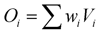 .4
.4
These bit cells are represented by the multistate compound MTJ. Each constituent MTJ on the compound MTJ comprises a MgO tunnel barrier sandwiched by the bottom CoFeB free layer of varying thickness (1.6–2.6 nm) and top-pinned CoFeB reference layer (Fig. 2a, See Methods). The cross-sectional scanning transmission electron microscopy (STEM) images with elemental mapping show the distinct layers of the MTJ (Fig. 2b and c). The plan view scanning electron microscopy imaging and cross-sectional TEM images of the compound MTJ show three elliptical MTJs of size 250 × 500 nm2 and spaced 1.2 μm apart on a shared Pt/Ta write channel of 0.9 × (0.9–3.25) μm2 (Fig. 2d and e). The spin orientations of the in-plane anisotropy CoFeB layers are aligned along the long axis of the elliptical MTJs, which correspond to the easy axis due to shape anisotropy, while the top RL is additionally pinned to a fixed orientation by the synthetic antiferromagnet layer. A current injected into the heavy metal Pt/Ta channel will generate a spin current at the Pt/CoFeB FL interface due to the spin Hall effect, inducing magnetization switching of the FL at a sufficiently large current density.25,26 An external magnetic field, H, is applied along with the SOT current to assist the FL switching in a preferable direction.
 | ||
| Fig. 2 Structural characterization of MTJs. (a) Schematic of the multilayer stack structure of the fabricated MTJs (thickness of layers are in nm in parentheses). (b) Cross-sectional scanning transmission electron microscopy (STEM) image of the multilayer stack structure (scale bar: 20 nm), and (c) corresponding energy-dispersive X-ray composition mapping. (d) Top view scanning electron microscopy (scale bar: 5 μm) and (e) cross-section TEM images (scale bar: 500 nm) of the compound device showing 3 MTJs on a shared SOT channel. | ||
The resistance dependence of the applied field, R(H), was acquired by sweeping a magnetic field (±20 mT) along the easy axis of the MTJs and measuring the output voltage through a reference resistor (1 MΩ) connected in series with the device under test. To examine the collective resistance dependence of applied voltage, R(V), the voltage pulses (amplitude: 0.1–2 V, width: 200 ns, and delay time: 1.5 s) are first applied across the write channel of the wire-bonded compound MTJ in the presence of an assisted H (±6 − 10 mT), followed by a readout of the compound MTJ resistance by injecting a small reading voltage of ∼0.1 V across the MTJ.
C. Free layer thickness variation
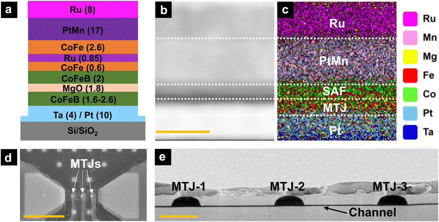
First, we examine the FL thickness dependence of magnetic and transport properties of the MTJ material stack and 1-cell devices. The major M(H) hysteresis loop of the MTJ film consisting of 1.6 nm-thick FL shows a defined step between the FL (∼±5 mT) and RL switching, indicating well-decoupled switching of FL independent of RL (Fig. 3a). Meanwhile, the major R(H) loop (Fig. 3b) of the corresponding device depicts a parallel (P) aligned RL and FL at large applied H of +300 mT. With a reduction in applied H to +90 mT, the exchange coupling between the SAF and RL dominates over the Zeeman energy of the external magnetic field, resulting in the rotation of the RL and FL to an antiparallel (AP) configuration and an increased resistance of 33.8 kΩ. Further reduction of H to −10 mT results in the switching of the FL, giving rise to a P configuration with a low resistance of 25.2 kΩ. Similar major M(H) and R(H) loops are observed across all FL thicknesses with well-decoupled switching of FL and RL, albeit with coercivity, Hc, and saturation field, Hs, variations to be discussed in the following paragraph. | ||
| Fig. 3 Magnetic and transport characteristics of the MTJ film and device. (a) and (b) Major (a) film-level M(H) and (b) device-level R(H) hysteresis loop for stack structure consisting of 1.6 nm-thick FL. (c) and (d) Minor (c) film-level M(H) and (d) device-level R(H) hysteresis loops for different FL thicknesses ranging from 1.6–2.6 nm. (e) and (f) The FL thickness dependence of (e) exchange field (Hex), coercive field (Hc), saturation field (Hs), and (f) antiparallel resistance (RAP), parallel resistance (RP), and tunneling magnetoresistance (TMR) extracted from the R(H) hysteresis loops measured across at least 10 devices for each free layer thickness. Solid lines in (e) and (f) are guides for the eye. | ||
Fig. 3c exhibits the minor M(H) hysteresis of the multilayer stacks for FL thickness ranging from 1.6–2.6 nm. As the FL thickness increases, the M(H) hysteresis with +x offset gradually shifts towards the left, marked by the diminishing exchange bias field, Hex, from 2.5 to 0.4 mT (Fig. 3e, violet diamond). This is due to the reduction of stray field effect on thicker FL, which originates from the lateral magnetic flux of the SAF layer and Néel coupling originated at the CFB/MgO interface.27 The increase in Hs from 12.7 to 14.8 mT suggests that the in-plane anisotropy along the easy-axis reduces with increasing FL thickness (Fig. 3e, black circle). Further, the coercive field, Hc, is constant to ∼12% across varying FL thicknesses of 1.6–2.6 nm (Fig. 3e, black square), wherein the fluctuation may be ascribed to inhomogeneity, structural defects, or localized disorder in the easy axis of the MTJ.28
The minor R(H) measurements across the MTJ devices of varying FL thickness show the sharp transition from the high resistance AP to low resistance P state for the down-field sweep, and vice versa, corresponding to the single domain-like characteristics expected in nanoscale 250 × 500 nm2 device (Fig. 3d). The device-level Hc are similar (∼10 mT ± 15%) across varying FL thicknesses, while 2× larger than the film-level Hc due to confinement effect which restricts domain motion and nucleation sites in the nanoscale MTJ.29,30 Due to the fabrication process variability and small uncompensated stray field from the SAF, a small positive or negative offset in the R(H) switching hysteresis is similarly observed.
Additionally, the resistances of the P (Fig. 3f, black circle) and AP (Fig. 3f, black square) states exhibit the same dome-like dependence of FL thickness, wherein the resistance increases to a plateau at intermediate FL thicknesses before decreasing at large FL thicknesses. This multifarious trend of resistance with increasing FL thickness is ascribed to interplaying factors of FL roughness31 and resistivity,32 variation in the MgO thickness,33 MgO/FL interface quality,34 and fabrication inhomogeneity at the circumference of the wafer. Meanwhile, the thickness dependence of TMR follows a near-exponential trend, marked by a gradual TMR increase from ∼33–40% for FL thickness <1.9 nm and a considerable surge from ∼40 to 78% for FL thickness >1.9 nm (Fig. 3f, violet diamond). The enhancement of TMR with increasing FL thickness is ascribed to the higher concentration of tunneling electrons and increase in the spin polarization in thicker FL,35 wherein the efficiency of spin filtering across the tunnel barrier remains independent of scattering effects for FL thickness up to 3 nm.
D. SOT switching
First, we examine the SOT-induced switching of the single-cell MTJs across different FL thicknesses of 1.6 to 2.6 nm. All the MTJs switch from the AP to P state when subjected to a negative applied V at a constant negative assisted magnetic field. Conversely, the FL switches from P to AP when a positive V is applied in the presence of a constant positive assisted magnetic field. This directional dependence of SOT mechanism is indicated by the full R(V) loop of the 1-cell MTJ of 1.7 nm free layer thickness (Fig. 4b) along with its corresponding R(H) curve (Fig. 4a). Notably, the critical switching voltage (Vc) increases from 0.7 to 2.0 V with increasing FL thickness from 1.6 to 2.6 nm (Fig. 4c). Expectedly, the dependence of critical current for SOT-induced switching on the FL thickness follows the relationship described by the macrospin model as follows:36| Ic = kMs(Hct + Mst − Ks)wHMtHM | (1) |
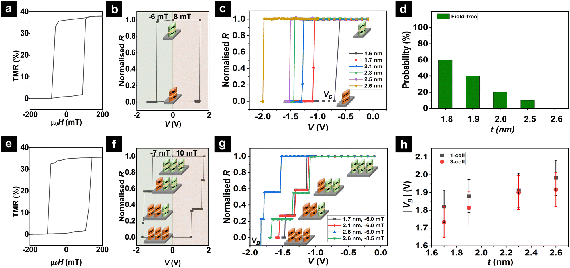 | ||
| Fig. 4 Electrical manipulation of compound MTJ. (a) R(H) and (b) R(V) loop for a 1-cell device comprising 1.7 nm-thick free layer. (c) The field-free R(V) plot of the 1-cell MTJ showing increasing critical switching voltage (Vc) for AP to P transition with increasing FL thickness. (d) Histogram plot showing the diminishing probability of field-free switching in 1-cell MTJs with increasing FL thickness. Up to 10 devices were measured for each FL thickness, of which all MTJs exhibit field-assisted switching. (e) R(H) and (f) R(V) loop for a 3-cell device comprising 1.7 nm-thick free layer. (g) The R(V) plot of the 3-cell MTJ for different FL thicknesses showing 4 resistance states in the presence of an assisted negative field of 6–8.5 mT. (h) The average breakdown voltage (VB) of the 1- and 3-cell MTJ for different FL thicknesses. Schematic inserts with arrows showing the free and reference layer spin orientations of each MTJ during the switching process. The MTJs in green and red represent the initial antiparallel and switched parallel configurations, respectively. The red (green) shade in (b) and (f) correspond to the P → AP (AP → P) transitions. | ||
Next, we study the SOT-induced switching of a multi-cell compound MTJ. Fig. 4e and f show the R(H) and R(V) loops for the 3-cell device comprising 1.7 nm-thick free layer, respectively. The 3-cell compound MTJ follows the resistor in-parallel relation, i.e., 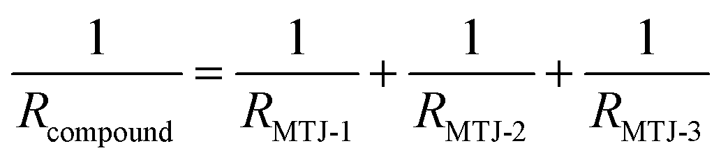 , and shows 4 resistance states corresponding to the switching of each constituent MTJ cell. For the same assisted magnetic field of −6 mT, the V required for fully switching the 3-cell compound MTJ from their AP to P states is ∼20–30% higher than the single cell-MTJ for the same FL thickness (Fig. 4g). In fact, a larger assisted magnetic field, e.g. −8.5 mT, is required to completely switch the thicker FL, e.g. 2.6 nm, without encountering the breakdown of the MTJ device. This is ascribed to the larger voltage drop across the more resistive (∼600 Ω) longer write channel of the 3-cell MTJ, compared to the single-cell MTJ channel of lower resistance (∼300 Ω).
Meanwhile, the trend of higher switching V for the devices with thicker FL is also similarly observed for the 3-cell MTJs (Fig. 4g). On one hand, as the FL thickness increases, the improvement in the TMR involves a compromise of energy efficiency. On the other hand, the average device breakdown voltage (VB) window extends from 1.8–2.0 V for 1-cell and 1.7–1.9 V for 3-cell when the FL thickness increases from 1.6 to 2.6 nm, suggesting that a thicker FL can better cushion device breakdown (Fig. 4h). However, the field-free switching of the FL is largely impeded by the VC > VB trend observed for thicker FL, hence switching of the thicker FL typically require an assisted field. Therefore, we posit that efforts towards the optimal performance of the MTJ-based neural network, beyond training and test accuracy, should also involve fine-tuning parameters of SOT switching efficiency and device breakdown voltage by optimizing the FL thickness, number of MTJ cells, and writing channel dimensions.
E. Spintronics artificial neural networks
The fabricated single and multistate MTJs can be harnessed to emulate neurons and synapses in an all-spin ANN as described in Fig. 1. Here, we show the neurons of the input, hidden and output layers of the ANN structured in a 784 × 128 × 10 configuration with sigmoidal activation functions (Fig. 5a). The synapses are emulated using 1-, 2-, and 3-cell compound MTJ devices where the conductance states of the MTJ devices represent the quantized synaptic weights. The ANNs are trained with 40 epochs to introduce precision weight distribution to the discrete 2-, 3-, 4- quantization levels of the pre-trained network. The trained ANN are subsequently subjected to digit and object recognition tasks and the respective test accuracies are determined.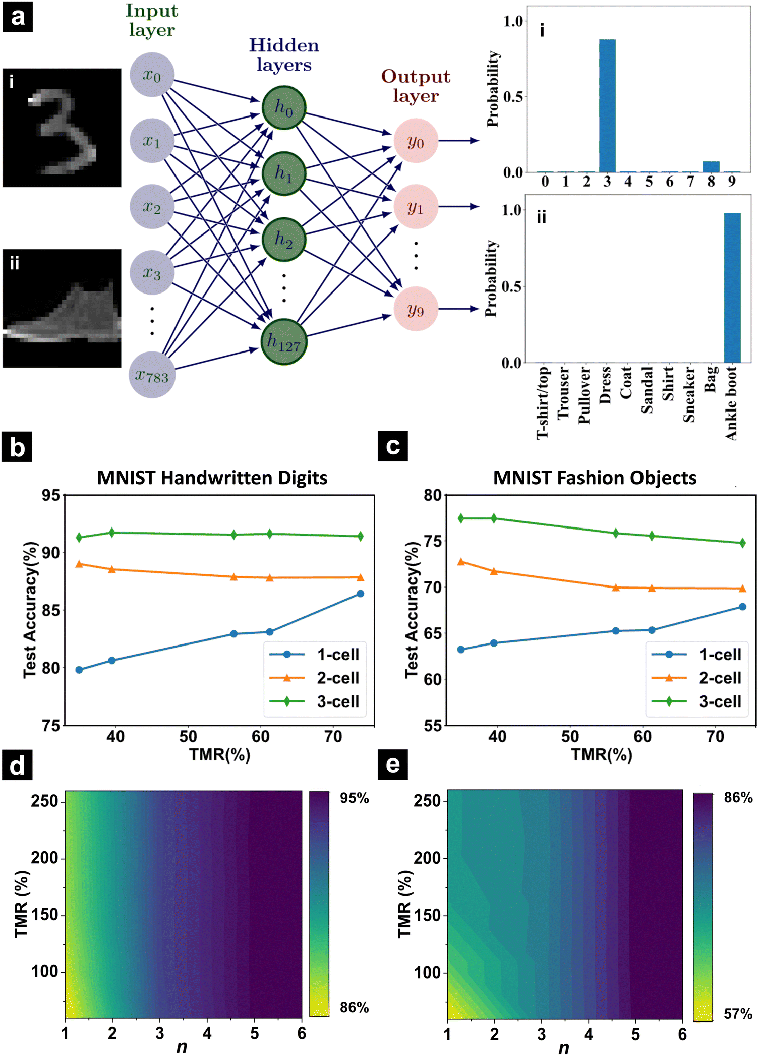 | ||
| Fig. 5 Bimodal tuning of cognitive accuracy for recognition tasks. (a) Schematic of the ANN constructed in a 784 × 128 × 10 configuration (middle) and illustrated with input examples of MNIST digits ((i), left) and fashion objects ((ii), left) and corresponding recognition probability ((i) and (ii), right). (b) and (c) The test accuracy for MNIST (b) handwritten digits and (c) fashion objects after training with 40 epochs for 1-, 2- and 3-cell MTJs. (d) and (e) 2D contour plots of the test accuracy for (d) handwritten digit and (e) fashion object recognition tasks as a function of TMR values and the number of MTJs of the synaptic device. The RP is arbitrarily fixed at 10 kΩ while the RAP is varied over the range of 16–36 kΩ to generate the TMR values of 60–260%. The test accuracies in detecting fashion objects are consistently poorer than recognizing digits for a particular number of cells and TMR. | ||
The test accuracies are simulated for various discrete states with increasing TMR values to gauge the combined impact of TMR and the number of discrete states. Fig. 5b illustrates the variation of test accuracy with TMR values for the MNIST handwritten digits dataset, across different numbers of discrete states. For 1-cell MTJ devices, the test accuracy rises by ∼8.3% with TMR values, following a direct correlation of accuracy with the ratio of the high and low conductance states of the synapses. Further, the test accuracy tends to increase more considerably, by up to ∼14.4%, with the number of MTJ in the devices due to the incremental number of available discrete conductance states for the synapses. For the 4-state weights, the 91% accuracy for digit recognition is acceptable for practical applications, and it greatly reduces the synaptic device size, leading to a lower footprint area and reduced complexity for the chip. Notably, the test accuracies for 2- and 3-MTJ devices exhibit a diversified trend with TMR, showing near-constant fluctuations of ±0.7% and 0.3%, respectively, as compared to the direct correlation of 1-cell MTJ devices. It could be ascribed to the compromised linearity of the synapse as new discrete states are introduced.
Additional testing of the ANN with the Fashion MNIST dataset shows similar trends, albeit with a decrease in overall accuracy due to the increased complexity of the Fashion database (Fig. 5c). The test accuracies decrease by approximately 4 and 3.45% for 2- and 3-MTJ devices, respectively, with an increase in TMR from 33 to 75%. This decline could be attributed to weight distribution in low-value discrete states, suggesting the potential benefit of employing more discrete states to address this issue. However, for datasets of higher complexity, either an increased number of discrete states, training samples,38 or advanced network architectures, such as convolutional networks,39,40 may be necessary to maintain performance levels.
To elucidate the interplaying effect of synaptic resolution and precision, we further model the ANNs built upon devices comprising an extended range of commercially viable TMR of 60–260% and 2–7 resistance states (Fig. 5d and e). Regardless of the TMR values, large cell numbers, e.g. 6-cell MTJs, produce consistently higher test accuracies for both digit and object recognition tasks. This suggests that the enhancement of synaptic precision induced by the multistate functionality plays a dominating role in elevating cognitive accuracies, as compared to synaptic resolution improvements defined by TMR modulation. Our findings guide future device efforts for realizing ANN endowed with both sizeable cognitive accuracies as well as high energy efficiency and robustness. This can be achieved by leveraging on the multistate MTJ device concept and moderate free layer thickness for optimal TMR and field-free switching, respectively.
F. Summary & outlook
In summary, we developed a spintronics ANN consisting of multistate compound SOT-MTJs with different FL thicknesses ranging from 1.6–2.6 nm. This enables a hybrid approach to tune the cognitive accuracies of the ANN by varying the number of resistance states and optimizing TMR, respectively. A large TMR difference of at least 21% between the states is obtained for the 3-cell MTJ, while a maximum TMR of 78% is observed for 2.6 nm-thick FL. The ANN constructed based on the 3-cell compound MTJ with 1.9 nm-thick FL exhibits the highest test accuracies of 91.7 and 77.4% for recognizing the MNIST handwritten digit and Fashion objects, respectively. Notably, the FL thickness in the compound MTJ should be chosen with high precision to reap the dual benefit of multilevels and high TMR, and in consideration for optimal SOT switching efficiency to obtain field-free switching.Our bimodal approach to achieve spin-based ANN with high cognitive accuracies will open novel paths for the realization of next-generation energy-efficient and robust neuroinspired computing devices for artificial intelligence at the edge. The neuromorphic hardware built upon the design of an array of MTJs on a shared write channel can be conveniently integrated into conventional CMOS technology. Future material efforts in realizing field-free energy-efficient switching with high synaptic precision can be achieved by incorporating appropriate heavy metal multilayers and alloys with high SOT efficiency.41 Meanwhile, further TMR enhancement can be achieved by fine-tuning the atomic structures of the ferromagnetic layers and tunneling barrier,42 or incorporating FLs such as CoNi and CoPt which manifest interface resonant tunneling.43 On the device front, the synaptic precision can be further enhanced by device designs that host manifold states of a sizable TMR ratio, such as creating multi-sized cells on the compound MTJ.44
G. Methods
Multilayer thin film fabrication
The MTJ multilayer stack consisting of SOT channel/FL/Tunnel barrier/RL/SAF/capping layer was fabricated on an 8-inch thermally oxidized Si-wafer using the Singulus TimarisTM DC magnetron sputtering at room temperature. Details of the multilayer stack composition and thicknesses (in nanometers) are as follows:(1) SOT channel: Ta (4)/Pt (10),
(2) FL: CoFeB (1.6–2.6),
(3) Tunnel barrier: MgO (1.8),
(4) RL: CoFeB (2),
(5) SAF: CoFe (0.6)/Ru (0.85)/CoFe (2.6)/PtMn (17),
(6) Capping layer: Ru (8).
The wafer was subsequently annealed in the magnetic vacuum annealing oven at 573 K for 60 minutes in the presence of a 1 T in-plane magnetic field applied along the wedge direction. The spin Hall angle of the Pt/CoFeB layers is ∼0.11.
Device fabrication
The MTJ multilayer stack was patterned into three-terminal compound MTJ devices by optical lithography using Canon EX5TM stepper and Ar-ion beam etching using Oxford CAIBETM. The device fabrication involved 5 key steps in creating the alignment mark, write channel, cell, open pad, and top electrode consisting of Ta (5)/Al (80)/Ru (5). The array of elliptical MTJs, of dimension 250 × 500 nm2, are patterned with their long axis along the wedge direction. For a particular FL thickness, a maximum of 18 dies can be segmented perpendicular to the wedge direction. The calculated device resistance-area lies in the range of 2.2–3.6 kΩ μm2 for the MTJ sizes of 250 × 500 nm2.Magnetic characterization
The multilayer thin film companion wafer, deposited along with the device wafer, was diced into 0.4 × 0.4 cm2 samples along the wedge direction. Magnetometry measurements were performed using the PrincetonTM alternating gradient magnetometer on the MTJ samples of varying thicknesses. The major and minor M(H) hysteresis loops of these diced multilayer thin film samples were obtained by performing a magnetic field sweep of ±1000 and ±20 mT, respectively, parallel to the inplane easy axis.Electrical measurements
The R(H) and R(V) measurements were performed using a custom-designed probe station equipped with AC lock-in (Zurich Instruments) in the presence of an assisted magnetic field (6 to 10 mT). To extract the FL thickness dependence of RAP, RP, and TMR, the R(H) loops were measured on at least ∼10 devices for each free layer thickness. For R(V) measurements, a train of voltage pulses (0.1–2.0 V, 200 ns, delay time: 1.5 s) was applied across the SOT channel using the Agilent pulse function generator, and the output voltage was measured across a reference resistor (1 MΩ) connected in series with the MTJ devices. The top electrodes of the constituent MTJ cells in the compound MTJ are connected to one another via wire bonding using the WESTBOND Inc., 7KFH, to obtain the collective response of the compound MTJs.Simulations
The performance evaluation of the spintronics-based ANN is conducted using TensorFlow,45 employing the MNIST handwritten digit dataset and the fashion object dataset. Each test sample (28 × 28 pixels) is normalized and converted into a column vector (784 pixels) to feed the input layer of the network. The sigmoid-like curve is considered for the activation function of the neuron while the network is trained with full precision weights employing the Adam optimizer,46 with the loss computed using sparse categorical cross-entropy. Subsequently, post successful training with full precision weights, both positive and negative weights are quantized based on experimentally measured conductance states (normalized) of our fabricated multistate MTJ devices. The 2, 3, and 4 state devices represent the synaptic bit precision for the simulation.Data availability
The data that support the findings of this study are available within the article.Conflicts of interest
The authors declare no competing interests.Acknowledgements
We acknowledge the helpful inputs from Prof. A. Soumyanarayanan and the technical help from S. Divanesh, G. K. Krishnaswamy, and D. V. Maheswar Repaka. This work is supported by the SpOT-LITE programme (Grant No. A18A6b0057), funded by Singapore's RIE2020 initiatives. This research is also supported by the RIE2025 Manufacturing, Trade and Connectivity (MTC) Individual Research Grant (Grant No. M23M6c0101) and Career Development Fund (Grant No. C210812017), administered by A*STAR.References
- D. Marković, A. Mizrahi, D. Querlioz and J. Grollier, Physics for Neuromorphic Computing, Nat. Rev. Phys., 2020, 2(9), 499–510, DOI:10.1038/s42254-020-0208-2.
- E. Donati and G. Valle, Neuromorphic Hardware for Somatosensory Neuroprostheses, Nat. Commun., 2024, 15(1), 1–18, DOI:10.1038/s41467-024-44723-3.
- C. D. Schuman, S. R. Kulkarni, M. Parsa, J. P. Mitchell, P. Date and B. Kay, Opportunities for Neuromorphic Computing Algorithms and Applications, Nat. Comput. Sci., 2022, 2(1), 10–19, DOI:10.1038/s43588-021-00184-y.
- A. Krogh, What Are Artificial Neural Networks?, Nat. Biotechnol., 2008, 26(2), 195–197, DOI:10.1038/nbt1386.
- C. Li, D. Belkin, Y. Li, P. Yan, M. Hu, N. Ge, H. Jiang, E. Montgomery, P. Lin, Z. Wang, W. Song, J. P. Strachan, M. Barnell, Q. Wu, R. S. Williams, J. J. Yang and Q. Xia, Efficient and Self-Adaptive in-Situ Learning in Multilayer Memristor Neural Networks, Nat. Commun., 2018, 9(1), 1–8, DOI:10.1038/S41467-018-04484-2.
- J. Woo, K. Moon, J. Song, S. Lee, M. Kwak, J. Park and H. Hwang, Improved Synaptic Behavior under Identical Pulses Using AlOx/HfO2 Bilayer RRAM Array for Neuromorphic Systems, IEEE Electron Dev. Lett., 2016, 37(8), 994–997, DOI:10.1109/LED.2016.2582859.
- M. Cassinerio, N. Ciocchini and D. Ielmini, Logic Computation in Phase Change Materials by Threshold and Memory Switching, Adv. Mater., 2013, 25(41), 5975–5980, DOI:10.1002/ADMA.201301940.
- B. Tian, L. Liu, M. Yan, J. Wang, Q. Zhao, N. Zhong, P. Xiang, L. Sun, H. Peng, H. Shen, T. Lin, B. Dkhil, X. Meng, J. Chu, X. Tang and C. Duan, A Robust Artificial Synapse Based on Organic Ferroelectric Polymer, Adv. Electron. Mater., 2019, 5(1), 1800600, DOI:10.1002/AELM.201800600.
- M. Yan, Q. Zhu, S. Wang, Y. Ren, G. Feng, L. Liu, H. Peng, Y. He, J. Wang, P. Zhou, X. Meng, X. Tang, J. Chu, B. Dkhil, B. Tian and C. Duan, Ferroelectric Synaptic Transistor Network for Associative Memory, Adv. Electron. Mater., 2021, 7(4), 2001276, DOI:10.1002/AELM.202001276.
- J. Grollier, D. Querlioz, K. Y. Camsari, K. Everschor-Sitte, S. Fukami and M. D. Stiles, Neuromorphic Spintronics, Nat. Electron., 2020, 3(7), 360–370, DOI:10.1038/S41928-019-0360-9.
- S. Jung, H. Lee, S. Myung, H. Kim, S. K. Yoon, S. W. Kwon, Y. Ju, M. Kim, W. Yi, S. Han, B. Kwon, B. Seo, K. Lee, G. H. Koh, K. Lee, Y. Song, C. Choi, D. Ham and S. J. Kim, A Crossbar Array of Magnetoresistive Memory Devices for In-Memory Computing, Nature, 2022, 601(7892), 211–216, DOI:10.1038/s41586-021-04196-6.
- Q. Yang, R. Mishra, Y. Cen, G. Shi, R. Sharma, X. Fong and H. Yang, Spintronic Integrate-Fire-Reset Neuron with Stochasticity for Neuromorphic Computing, Nano Lett., 2022, 22(21), 8437–8444 CrossRef CAS PubMed.
- H. Pourmeidani, P. Debashis, Z. Chen, R. F. Demara and R. Zand, Electrically-Tunable Stochasticity for Spin-Based Neuromorphic Circuits: Self-Adjusting to Variation, Midwest Symposium on Circuits and Systems, 2020, pp. 81–84 DOI:10.1109/MWSCAS48704.2020.9184556.
- S. Yang, J. Shin, T. Kim, K. W. Moon, J. Kim, G. Jang, D. S. Hyeon, J. Yang, C. Hwang, Y. J. Jeong and J. P. Hong, Integrated Neuromorphic Computing Networks by Artificial Spin Synapses and Spin Neurons, NPG Asia Mater., 2021, 13(1), 1–10, DOI:10.1038/s41427-021-00282-3.
- H. Cai, Z. Bian, Z. Fan, B. Liu and L. Naviner, Commodity Bit-Cell Sponsored MRAM Interaction Design for Binary Neural Network, IEEE Trans. Electron Devices, 2022, 69(4), 1721–1726, DOI:10.1109/TED.2021.3134588.
- R. Chen, C. Li, Y. Li, J. J. Miles, G. Indiveri, S. Furber, V. F. Pavlidis and C. Moutafis, Nanoscale Room-Temperature Multilayer Skyrmionic Synapse for Deep Spiking Neural Networks, Phys. Rev. Appl., 2020, 14(1), 014096, DOI:10.1103/PHYSREVAPPLIED.14.014096/FIGURES/10/MEDIUM.
- D. Zhang, L. Zeng, Y. Qu, Y. Zhang, Z. M. Wang, W. Zhao, T. Tang and Y. Wang Energy-Efficient Neuromorphic Computation Based on Compound Spin Synapse with Stochastic Learning, 2015 IEEE International Symposium on Circuits and Systems (ISCAS), IEEE, 2015, 1538–1541 DOI:10.1109/ISCAS.2015.7168939.
- T. Moposita, E. Garzon, F. Crupi, L. Trojman, A. Vladimirescu and M. Lanuzza, Efficiency of Double-Barrier Magnetic Tunnel Junction-Based Digital ENVM Array for Neuro-Inspired Computing, IEEE Trans. Circuits Syst., 2023, 70(3), 1254–1258, DOI:10.1109/TCSII.2023.3240474.
- D. Zhang, L. Zeng, K. Cao, M. Wang, S. Peng, Y. Zhang, Y. Zhang, J. O. Klein, Y. Wang and W. Zhao, All Spin Artificial Neural Networks Based on Compound Spintronic Synapse and Neuron, IEEE Trans. Circuits Syst., 2016, 10(4), 828–836, DOI:10.1109/TBCAS.2016.2533798.
- A. Kumar, D. J. X. Lin, D. Das, L. Huang, S. L. K. Yap, H. R. Tan, H. K. Tan, R. J. J. Lim, Y. T. Toh, S. Chen, S. T. Lim, X. Fong and P. Ho, Multistate Compound Magnetic Tunnel Junction Synapses for Digital Recognition, ACS Appl. Mater. Interfaces, 2024, 16(8), 10335–10343, DOI:10.1021/ACSAMI.3C17195/SUPPL_FILE/AM3C17195_SI_001.PDF.
- K. Y. Camsari, B. M. Sutton and S. Datta, P-Bits for Probabilistic Spin Logic, Appl. Phys. Rev., 2019, 6, 011305, DOI:10.1063/1.5055860/570987.
- T. Leonard, S. Liu, M. Alamdar, H. Jin, C. Cui, O. G. Akinola, L. Xue, T. P. Xiao, J. S. Friedman, M. J. Marinella, C. H. Bennett and J. A. C. Incorvia, Shape-Dependent Multi-Weight Magnetic Artificial Synapses for Neuromorphic Computing, Adv. Electron. Mater., 2022, 8(12), 2200563, DOI:10.1002/aelm.202200563.
- E. Raymenants, O. Bultynck, D. Wan, T. Devolder, K. Garello, L. Souriau, A. Thiam, D. Tsvetanova, Y. Canvel, D. E. Nikonov, I. A. Young, M. Heyns, B. Soree, I. Asselberghs, I. Radu, S. Couet and V. D. Nguyen, Nanoscale Domain Wall Devices with Magnetic Tunnel Junction Read and Write, Nat. Electron., 2021, 4(6), 392–398, DOI:10.1038/s41928-021-00593-x.
- S. A. Siddiqui, S. Dutta, A. Tang, L. Liu, C. A. Ross and M. A. Baldo, Magnetic Domain Wall Based Synaptic and Activation Function Generator for Neuromorphic Accelerators, Nano Lett., 2020, 20(2), 1033–1040, DOI:10.1021/acs.nanolett.9b04200.
- C. Song, R. Zhang, L. Liao, Y. Zhou, X. Zhou, R. Chen, Y. You, X. Chen and F. Pan, Spin-Orbit Torques: Materials, Mechanisms, Performances, and Potential Applications, Prog. Mater. Sci., 2021, 118, 100761, DOI:10.1016/J.PMATSCI.2020.100761.
- Q. Shao, P. Li, L. Liu, H. Yang, S. Fukami, A. Razavi, H. Wu, K. Wang, F. Freimuth, Y. Mokrousov, M. D. Stiles, S. Emori, A. Hoffmann, J. Akerman, K. Roy, J. P. Wang, S. H. Yang, K. Garello and W. Zhang, Roadmap of Spin-Orbit Torques, IEEE Trans. Magn., 2021, 57, 800439, DOI:10.1109/TMAG.2021.3078583.
- J. D. Costa, S. Serrano-Guisan, J. Borme, F. L. Deepak, M. Tarequzzaman, E. Paz, J. Ventura, R. Ferreira and P. P. Freitas, Impact of MgO Thickness on the Performance of Spin-Transfer Torque Nano-Oscillators, IEEE Trans. Magn., 2015, 51, 1401604, DOI:10.1109/TMAG.2015.2441141.
- L. Kipgen, H. Fulara, M. Raju and S. Chaudhary, In-Plane Magnetic Anisotropy and Coercive Field Dependence upon Thickness of CoFeB, J. Magn. Magn. Mater., 2012, 324(19), 3118–3121, DOI:10.1016/J.JMMM.2012.05.012.
- W. B. Liao, C. Y. Lin, T. Y. Cheng, C. C. Huang, T. Y. Chen and C. F. Pai, Processing Effect on Spin-Orbit Torque Switching and Efficiency Characterization in Perpendicularly Magnetized Pillar Devices, Phys. Rev. Mater., 2023, 7(10), 104409, DOI:10.1103/PHYSREVMATERIALS.7.104409/FIGURES/4/MEDIUM.
- H. Liu, H. Wei, X. Han, G. Yu, W. Zhan, S. Le Gall, Y. Lu, M. Hehn, S. Mangin, M. Sun, Y. Liu and C. Horng, Magnetic Configurations and State Diagram of Nanoring Magnetic Tunnel Junctions, Phys. Rev. Appl., 2018, 10(5), 054013, DOI:10.1103/PHYSREVAPPLIED.10.054013/FIGURES/6/MEDIUM.
- C. Durner, M. Lederer, T. Gurieva, J. Hertel, M. Hindenberg, L. Gerlich, M. Wagner-Reetz and S. Parkin, Influence of Free Layer Surface Roughness on Magnetic and Electrical Properties of 300 Mm CMOS-Compatible MTJ Stacks, IEEE Trans. Magn., 2023, 59, 4400404, DOI:10.1109/TMAG.2023.3287134.
- Y. T. Chen and S. M. Xie, Magnetic and Electric Properties of Amorphous Co 40Fe 40B 20 Thin Films, J. Nanomater., 2012, 2012, DOI:10.1155/2012/486284.
- T. Nozaki, T. Nozaki, T. Yamamoto, M. Konoto, A. Sugihara, K. Yakushiji, H. Kubota, A. Fukushima and S. Yuasa, Enhancing the Interfacial Perpendicular Magnetic Anisotropy and Tunnel Magnetoresistance by Inserting an Ultrathin LiF Layer at an Fe/MgO Interface, NPG Asia Mater., 2022, 14(1), 1–7, DOI:10.1038/s41427-021-00350-8.
- M. Zhu, H. Chong, Q. B. Vu, R. Brooks, H. Stamper and S. Bennett, Study of CoFeB Thickness and Composition Dependence in a Modified CoFeB/MgO/CoFeB Perpendicular Magnetic Tunnel Junction, J. Appl. Phys., 2016, 119(7), 73907, DOI:10.1063/1.4942166/142325.
- C. Y. Yang, S. J. Chang, M. H. Lee, K. H. Shen, S. Y. Yang, H. J. Lin and Y. C. Tseng, Competing Anisotropy-Tunneling Correlation of the CoFeB/MgO Perpendicular Magnetic Tunnel Junction: An Electronic Approach, Sci. Rep., 2015, 5(1), 1–9, DOI:10.1038/srep17169.
- S. Shi, Y. Ou, S. V. Aradhya, D. C. Ralph and R. A. Buhrman, Fast Low-Current Spin-Orbit-Torque Switching of Magnetic Tunnel Junctions through Atomic Modifications of the Free-Layer Interfaces, Phys. Rev. Appl., 2018, 9(1), 011002, DOI:10.1103/PHYSREVAPPLIED.9.011002/FIGURES/3/MEDIUM.
- M. Bersweiler, E. C. I. Enobio, S. Fukami, H. Sato and H. Ohno, An Effect of Capping-Layer Material on Interfacial Anisotropy and Thermal Stability Factor of MgO/CoFeB/Ta/CoFeB/MgO/Capping-Layer Structure, Appl. Phys. Lett., 2018, 113, 172401, DOI:10.1063/1.5050486/839808.
- D. Wang, R. Tang, H. Lin, L. Liu, N. Xu, Y. Sun, X. Zhao, Z. Wang, D. Wang, Z. Mai, Y. Zhou, N. Gao, C. Song, L. Zhu, T. Wu, M. Liu and G. Xing, Spintronic Leaky-Integrate-Fire Spiking Neurons with Self-Reset and Winner-Takes-All for Neuromorphic Computing, Nat. Commun., 2023, 14(1), 1–12, DOI:10.1038/s41467-023-36728-1.
- Y. Lecun, Y. Bengio and G. Hinton, Deep Learning, Nature, 2015, 521(7553), 436–444, DOI:10.1038/nature14539.
- N. Leroux, A. De Riz, D. Sanz-Hernández, D. Marković, A. Mizrahi and J. Grollier, Convolutional Neural Networks with Radio-Frequency Spintronic Nano-Devices, Neuromorphic Comput. Eng., 2022, 2(3), 034002, DOI:10.1088/2634-4386/AC77B2.
- C. Y. Hu and C. F. Pai, Benchmarking of Spin–Orbit Torque Switching Efficiency in Pt Alloys, Adv. Quantum. Technol., 2020, 3(8), 2000024, DOI:10.1002/QUTE.202000024.
- T. Scheike, Z. Wen, H. Sukegawa and S. Mitani, 631% Room Temperature Tunnel Magnetoresistance with Large Oscillation Effect in CoFe/MgO/CoFe(001) Junctions, Appl. Phys. Lett., 2023, 122(11), 112404, DOI:10.1063/5.0145873/2880999.
- K. Masuda, H. Itoh, Y. Sonobe, H. Sukegawa, S. Mitani and Y. Miura, Interfacial Giant Tunnel Magnetoresistance and Bulk-Induced Large Perpendicular Magnetic Anisotropy in (111)-Oriented Junctions with Fcc Ferromagnetic Alloys: A First-Principles Study, Phys. Rev. B, 2021, 103(6), 064427, DOI:10.1103/PHYSREVB.103.064427/FIGURES/9/MEDIUM.
- A. H. Lone, S. Shringi, K. Mishra and S. Srinivasan, Cross-Sectional Area Dependence of Tunnel Magnetoresistance, Thermal Stability, and Critical Current Density in MTJ, IEEE Trans. Magn., 2021, 57(2), 4400410, DOI:10.1109/TMAG.2020.3039682.
- M. Abadi; A. Agarwal; P. Barham; E. Brevdo; Z. Chen; C. Citro; G. S. Corrado; A. Davis; J. Dean; M. Devin; S. Ghemawat; I. Goodfellow; A. Harp; G. Irving; M. Isard; Y. Jia; R. Jozefowicz; L. Kaiser; M. Kudlur; J. Levenberg; D. Mane; R. Monga; S. Moore; D. Murray; C. Olah; M. Schuster; J. Shlens; B. Steiner; I. Sutskever; K. Talwar; P. Tucker; V. Vanhoucke; V. Vasudevan; F. Viegas; O. Vinyals; P. Warden; M. Wattenberg; M. Wicke; Y. Yu and X. Zheng TensorFlow: Large-Scale Machine Learning on Heterogeneous Distributed Systems. 2016.
- D. P. Kingma and J. Ba Adam: A Method for Stochastic Optimization. 3rd International Conference on Learning Representations, ICLR 2015 - Conference Track Proceedings 2014.
| This journal is © The Royal Society of Chemistry 2024 |