 Open Access Article
Role of antisolvent temperature and quaternary ammonium cation-based ionic liquid engineering in the performance of perovskite solar cells processed under air ambient conditions†
Subrata
Ghosh
 *a,
Binita
Boro
b,
Shivam
Porwal
 a,
Snehangshu
Mishra
 a and
Trilok
Singh
 *abc
*abc
aFunctional Materials and Device Laboratory, School of Energy Science and Engineering, Indian Institute of Technology, Kharagpur, 721302, India. E-mail: subrata.subho7@gmail.com; triloksingh@dese.iitd.ac.in
bSchool of Nano Science and Technology, Indian Institute of Technology, Kharagpur, 721302, India
cDepartment of Energy Science and Engineering, Indian Institute of Technology Delhi, Hauz Khas, New Delhi 110016, India
First published on 5th June 2023
Abstract
Perovskite solar cells are becoming one of the strong contenders for renewable energy generation sources. However, to make the technology available on the market and commercially successful, efficient and stable perovskite solar cells must be fabricated under ambient conditions. Herein, a combination of antisolvent and ionic liquid engineering is applied to produce efficient and stable perovskite solar cells under ambient conditions. Chlorobenzene antisolvent of low-temperature produces compact perovskite films and better interfacial contact. A quaternary ammonium cation-based ionic liquid, trimethylpropylammonium bis(trifluoromethanesulfonyl)imide [TMPA][TFSI], is applied at the TiO2/perovskite interface to passivate the interfacial defects and improve the electron transfer efficiency. The combined effect of low-temperature chlorobenzene antisolvent (5 °C) and 0.01 M [TMPA][TFSI] resulted in a power conversion efficiency enhancement of over 16% as compared to pristine devices. Interestingly, the optimized devices showed high stability and retained above 90% efficiency after 1500 h of dark storage with a periodic measurement under ambient conditions.
1. Introduction
Perovskite solar cells (PSCs) are the most significant next-generation solar cell technology, with a magnificent highest power conversion efficiency (PCE) of 25.7% (2023), a whopping jump from 3.8% (2009) within fourteen years of invention.1–6 Halide perovskites exhibit excellent optoelectronic properties – optimum and tunable bandgap, considerable charge carrier diffusion length, high absorption coefficient and low exciton binding energy.7–13 In addition, perovskite solar cells are cheap and solution processable.14 However, perovskite solar cell fabrication, which is a solution process route, leads to poor-quality films and interfaces.15–17 Poor-quality films could have many pinholes and not completely cover the substrate, leading to low light absorption and facilitating current leakage pathways. Besides, poor-quality interfaces create many issues, such as interfacial defects, energy band misalignment and inefficient charge transfer. Furthermore, poor interfaces provide pathways for moisture and oxygen penetration.18–21Antisolvent dripping during the perovskite film fabrication improves the uniformity and surface coverage of the film by enhancing the nucleation.22 Various antisolvents, like chlorobenzene, toluene, ethyl acetate, dichloromethane, diethyl ether, and anisole, are used.23–28 Jeon et al. utilized toluene to obtain a homogeneous, pinhole-free and smoother CH3NH3Pb(I1−xBrx)3-based perovskite film and achieved a PCE of 16.02%.29 Singh et al. explored the beneficial effect of antisolvents using chlorobenzene, toluene and ethyl acetate. Although all the antisolvents improved the triple cation-based perovskite film quality and device performance, chlorobenzene led to the highest efficiency of 20.1% in that study.30 Interestingly, the antisolvent temperature also influences the quality of the perovskite film. A study by Ren et al. revealed that low-temperature chlorobenzene (0 °C) led to better (FAPbI3)0.85(MAPbBr3)0.15-based perovskite film quality and device performance compared to higher-temperature chlorobenzene (20 °C and 40 °C).31 On the contrary, Taherianfard et al. observed that a chlorobenzene temperature of 35 °C resulted in the highest efficiency of double cation (MA, FA) mixed halide (I, Br) lead perovskite-based devices, while lower temperatures (0 °C and 20 °C) and higher temperatures (50 °C and 100 °C) of chlorobenzene showed comparatively inferior device performance.32 The optimum temperature of the antisolvent could vary depending on the perovskite composition, antisolvent and fabrication conditions.
Furthermore, ionic liquids have proved to be potential chemicals for improvement in perovskite film and interface quality.33–35 For instance, Yang et al. improved the efficiency from 16.45% to 19.62% and eliminated hysteresis by applying 1-butyl-3-methylimidazolium tetrafluoroborate, [BMIM]BF4 ionic liquid at the TiO2/perovskite interface, which passivated the interfacial defects and improved the charge transfer at the interface.36 Zhang et al. used 1-ethyl-3-methylimidazolium hexafluorophosphate, [EMIM]PF6 ionic liquid at the ZnO/MAPbI3 interface to improve the perovskite film quality and passivate the defects at the interface. As a result, improvement in efficiency and suppression in hysteresis were observed.37 In addition, Noel et al. observed that upon applying [BMIM]BF4 ionic liquid at the SnO2/FA0.83MA0.17Pb(I0.83Br0.17)3 interface, the n-type nature of the perovskite enhances along with other benefits like interfacial defect passivation.38 In the literature, most of the ionic liquid modifications in perovskite solar cells have been done with imidazolium cation-based ionic liquids,36–41 which are relatively more hygroscopic.42,43 On the other hand, quaternary ammonium cation-based ionic liquids have not been explored in perovskite solar cells, which could have potential for interfacial engineering in PSCs.
Generally, PSCs are fabricated inside a glove box with a controlled atmosphere due to the sensitivity towards moisture and oxygen to achieve high efficiency. However, fabrication techniques must be developed under the ambient atmosphere to commercialize the bulk production of PSCs. On a positive note, many studies have recently been done under ambient conditions.30,44–49 Nonetheless, further rigorous studies under ambient conditions are required to accelerate the commercialization of PSCs.
Against this backdrop, in this study, the effect of chlorobenzene antisolvent temperature on triple cation mixed halide perovskite [Cs0.05(FA0.83MA0.17)0.95Pb(I0.83Br0.17)3]-based film and device performance are observed and analyzed. After optimizing the antisolvent temperature, a quaternary ammonium cation-based ionic liquid – trimethylpropylammonium bis(trifluoromethanesulfonyl)imide [TMPA][TFSI] is used at the TiO2/perovskite interface to improve the device performance. Importantly, the PSCs are fabricated under ambient conditions, with controlled humidity (RH = 25 ± 5%). The optimized parameters resulted in high efficiency and stability of the ambient condition-fabricated PSCs. The champion device achieved a PCE of 19.04%, and the optimized devices retained >90% of the initial PCE after 1500 h of dark storage under ambient conditions.
2. Experimental section
Materials
The chemicals used in this study were used as received from the company without further purification. Hellmanex soap, titanium diisopropoxide bis(acetylacetonate) 75 wt% in isopropanol, and spiro-OMeTAD (99%) were purchased from Sigma-Aldrich. Trimethylpropylammonium bis(trifluoromethanesulfonyl)imide (>98%), lead iodide (PbI2) (99.99%), formamidinium iodide (FAI) (99.99%), methylammonium bromide (MABr) (>98.0%), lead bromide (PbBr2) (>98.0%), cesium iodide (CsI) (>99.0%), 4-tert-butylpyridine (>96.0%), and lithium bis(trifluoromethanesulfonyl)imide (>98.0%) were purchased from Tokyo Chemical Industry (TCI). Titanium(IV) chloride (TiCl4) (>97.0%), isopropanol (>99.5%), acetone (>99.5%), dimethyl sulfoxide (DMSO) (>99.0%), N,N-dimethylformamide (DMF) (>99.5%), acetonitrile (ACN) (>99%) and chlorobenzene (CB) (>99.5%) were purchased from Merck. 2.2 mm thick FTO-coated glass plates were purchased from Greatcell Solar Materials.Device fabrication
FTO-coated glass substrates (2.5 × 2.5 cm2) were cleaned sequentially with 2% Hellmanex solution, DI water, acetone and isopropanol for 30 min each using ultrasonication. Before coating the TiO2 compact layer, the substrates were subjected to UV-O3 cleaning for 15 min. For the TiO2 compact layer, three consecutive coatings (3000 rpm) of 0.15 M, 0.3 M and 0.15 M titanium diisopropoxide bis(acetylacetonate) solution were done. The substrates were kept at 130 °C for 5 min after each coating and finally annealed at 500 °C for 1 h. Then the substrates were treated with 0.04 M aqueous solutions of TiCl4 at 70 °C for 1 h and then thoroughly rinsed with DI water, followed by annealing at 500 °C for 30 min. After that, the substrates were spin-coated (2000 rpm) with 0.1 M lithium bis(trifluoromethanesulfonyl)imide solution in acetonitrile and kept at 450 °C for 30 min. For the perovskite precursor solution FAI (1 M), PbI2 (1.1 M), MABr (0.2 M), and PbBr2 (0.2 M) were dissolved in DMF![[thin space (1/6-em)]](https://www.rsc.org/images/entities/char_2009.gif) :
:![[thin space (1/6-em)]](https://www.rsc.org/images/entities/char_2009.gif) DMSO (4
DMSO (4![[thin space (1/6-em)]](https://www.rsc.org/images/entities/char_2009.gif) :
:![[thin space (1/6-em)]](https://www.rsc.org/images/entities/char_2009.gif) 1). Next, 41 μL of 1.5 M CsI solution in DMSO was added into 1 mL of the perovskite precursor solution. The solution was then kept at 65 °C and stirred vigorously for 1 h. The precursor solution was then spin-coated on the Li-doped TiO2 layer in two steps (i) 1200 rpm for 15 s, (ii) 5000 rpm for 30 s. 300 μL of chlorobenzene antisolvent was dripped at the 15th s of the 2nd step. Then the substrates are immediately transferred to a hot plate and annealed at 108 °C for 1 h under the cover of a Petri dish. Then, 60 mg of Spiro-OMeTAD was dissolved in 624 μL of chlorobenzene, and 24 μL of 0.6 M lithium bis(trifluoromethanesulfonyl)imide solution in acetonitrile and 11.5 μL of 4-tert-butylpyridine were added to the solution. The spiro-OMeTAD solution was then spin-coated at 2000 rpm for 30 s on the perovskite layer. Finally, 80 nanometre (nm) of gold was deposited by thermal evaporation for the back contact. For the ionic liquid-modified devices, a solution of [TMPA][TFSI] ionic liquid in isopropanol was spin-coated (5000 rpm for 45 s) on Li-doped TiO2 and kept at 100 °C for 15 min.
1). Next, 41 μL of 1.5 M CsI solution in DMSO was added into 1 mL of the perovskite precursor solution. The solution was then kept at 65 °C and stirred vigorously for 1 h. The precursor solution was then spin-coated on the Li-doped TiO2 layer in two steps (i) 1200 rpm for 15 s, (ii) 5000 rpm for 30 s. 300 μL of chlorobenzene antisolvent was dripped at the 15th s of the 2nd step. Then the substrates are immediately transferred to a hot plate and annealed at 108 °C for 1 h under the cover of a Petri dish. Then, 60 mg of Spiro-OMeTAD was dissolved in 624 μL of chlorobenzene, and 24 μL of 0.6 M lithium bis(trifluoromethanesulfonyl)imide solution in acetonitrile and 11.5 μL of 4-tert-butylpyridine were added to the solution. The spiro-OMeTAD solution was then spin-coated at 2000 rpm for 30 s on the perovskite layer. Finally, 80 nanometre (nm) of gold was deposited by thermal evaporation for the back contact. For the ionic liquid-modified devices, a solution of [TMPA][TFSI] ionic liquid in isopropanol was spin-coated (5000 rpm for 45 s) on Li-doped TiO2 and kept at 100 °C for 15 min.
Materials and device characterizations
Morphological characterization (SEM) is done by a field emission gun SEM (Zeiss MERLIN). An Agilent 5500 is utilized for topological characterization (AFM). XRD patterns are generated using a Bruker D8 Discover Diffractometer System. UV-vis absorption spectroscopy is done by using an Avantes Starline AvaSpec-ULS364 UV-vis spectrometer. Photoluminescence characterizations are done by a Horiba iHR 320 spectrometer. XPS measurements are done using a PHI 5000 VERSA PROBE III model. FTIR is done using a Bruker LUMOS II model. A Peccell Technologies PEC-L01 solar simulator is used to generate the AM 1.5G simulated spectrum of 100 mW cm−2 intensity. A Keithley 2450 SMU is used to carry out the J–V measurements. All the devices are kept unencapsulated for stability measurements under dark ambient conditions.3. Results and discussion
3.1 Variation in antisolvent temperature
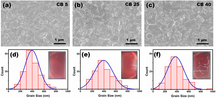
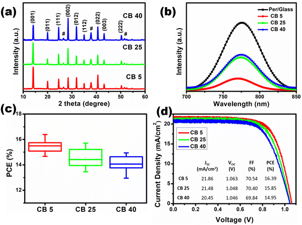
Three temperatures of chlorobenzene are chosen, 5 °C, 25 °C and 40 °C, to study the temperature effect of the antisolvent. Samples fabricated using chlorobenzene of 5 °C, 25 °C, and 40 °C have been denoted as CB 5, CB 25 and CB 40, respectively. The optical images of the fabricated perovskite films show that CB 5 and CB 25 do not contain any visible pinholes (inset: Fig. 1(d) and (e)). However, CB 40 has visible cracks, which could be due to the rapid evaporation of chlorobenzene and fast initial grain growth at a higher temperature (inset: Fig. 1(f)). The SEM images show pinhole-free perovskite films in all the cases (Fig. 1(a)–(c)). However, subtle morphological differences have been observed after grain size analysis. Although the average grain size is approx. 400 nm in all the samples, the grain size distribution is narrow in CB 5, whereas the distribution is broader in CB 25 and CB 40 (Fig. 1(d)–(f)). The narrow grain size distribution in CB 5 is attributed to the uniform nucleation of the perovskite. In addition, the nucleation is higher at a lower temperature, evident from the grain count in the SEM images. The cross-section SEM images of the complete devices (Fig. S2, ESI†) reveal that the average thickness of the perovskite layers is approx. 620 nm and does not get affected by the antisolvent temperature.The XRD patterns of the perovskite films show strong peaks of the perovskite phase without any PbI2 impurity peaks, which indicates the complete conversion of precursors into the perovskite phase (Fig. 2(a)). The FWHM of the (001) peak for the CB 5, CB 25 and CB 40 samples is 0.272°, 0.265° and 0.266°, respectively (Fig. S3, ESI†), which indicates that the crystallite sizes are slightly smaller in the CB 5 samples than the CB 25 and CB 40 samples. However, the relative intensity of the (001) peak to the intensity of the (111) peak and (200) peak shows an increasing trend with the decrease in antisolvent temperature, indicating higher preferential crystal orientation in the (100) plane.50 The UV-Vis absorption spectroscopy of the films reveals higher absorption in the visible spectrum for CB 5, followed by CB 25 and CB 40 (Fig. S4, ESI†). Higher absorption in CB 5 indicates a more compact film compared to others, which is also corroborated by the SEM images. Steady-state photoluminescence (PL) of the perovskite films deposited on the TiO2 electron transport layer (ETL) is done to understand the TiO2/perovskite interface quality (Fig. 2(b)). The chlorobenzene temperature influences the PL spectra quenching. The order of PL spectra quenching is CB 5 > CB 25 > CB 40, which signifies that the electron transfer from the perovskite to TiO2 is most efficient in CB 5, followed by CB 25, followed by CB 40. Higher electron transfer efficiency in CB 5 is attributed to better TiO2/perovskite interface quality. Slow initial perovskite crystallization and homogeneous distribution of the grains in the CB 5 samples resulted in less disorder and robust contact at the TiO2/perovskite interface, which facilitates efficient electron transfer. A slight blue shift in the PL spectra can be observed in the low-temperature antisolvent-treated sample (CB 5). This blue shift can be attributed to the relatively smaller crystallite sizes in the CB 5 samples.51,52
Furthermore, to investigate the effect of antisolvent temperature, optical microscopic images of the perovskite films are taken immediately after the dripping of the antisolvent without any heat treatment (Fig. S5, ESI†). It is observed that low-temperature antisolvent (CB 5) dripping leads to slow and homogeneous initial grain growth, indicated by uniformly spaced black dots in the image. In the case of the CB 25 sample, the initial grain growth is almost homogeneous with several large dark regions. However, in the CB 40 sample, it can be observed that the initial grain growth is not homogeneous and comparatively fast (spacious and large black dots).
The solar cell devices are fabricated as the following structure – FTO/TiO2/perovskite/spiro-OMeTAD/Au. At least seventeen devices are considered from each category for analysis of J–V performance. It is observed that CB 5 devices show better performances (Table 1). The average JSC of the CB 5 (20.96 ± 0.60 mA cm−2) devices is higher than that of CB 25 (20.75 ± 0.51 mA cm−2) and CB 40 (20.48 ± 0.36 mA cm−2) devices (Fig. S6a, ESI†). The better JSC of CB 5 is owing to better interface quality at the TiO2/perovskite interface, which is substantiated by the quenching of steady-state PL spectra. The average VOC of the CB 5 devices is 1.051 ± 0.014 V, which is higher than the average VOC of CB 25 (1.047 ± 0.017 V) and CB 40 (1.044 ± 0.012 V) devices (Fig. S6b, ESI†). The better VOC of CB 5 devices could be attributed to reduced defect density due to slow initial grain growth at low temperature. The average FF of the CB 5 (70.60 ± 1.65%) devices is also higher than that of CB 25 (67.77 ± 2.11%) and CB 40 (65.65 ± 2.72%) devices (Fig. S6c, ESI†), which is due to the reduction in series resistance RS (due to compact interface and reduced defects at the interface). The improved JSC, VOC and FF ultimately led to enhanced PCE of CB 5 devices. The average PCE of CB 5 devices is 15.45 ± 0.49%, with the highest PCE of 16.39%. On the other hand, the average PCE of CB 25 and CB 40 devices is 14.58 ± 0.69% and 14.10 ± 0.58%, respectively, with the highest PCE of 15.85% and 14.95%, respectively (Fig. 2(c)). The J–V curves of the highest-performing devices are shown in Fig. 2(d).
| J SC (mA cm−2) | V OC (V) | FF (%) | PCE (%) | ||
|---|---|---|---|---|---|
| CB 5 | Average | 20.96 ± 0.60 | 1.051 ± 0.014 | 70.60 ± 1.65 | 15.45 ± 0.49 |
| Best cell | 21.86 | 1.063 | 70.54 | 16.39 | |
| CB 25 | Average | 20.75 ± 0.51 | 1.047 ± 0.017 | 67.77 ± 2.11 | 14.58 ± 0.69 |
| Best cell | 21.48 | 1.048 | 70.40 | 15.85 | |
| CB 40 | Average | 20.48 ± 0.36 | 1.044 ± 0.012 | 65.65 ± 2.72 | 14.10 ± 0.58 |
| Best cell | 20.45 | 1.046 | 69.84 | 14.95 | |
3.2 Ionic liquid at the TiO2/perovskite interface
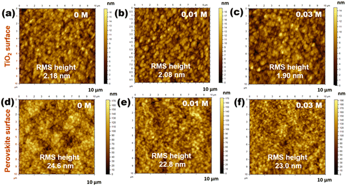
Trimethylpropylammonium bis(trifluoromethanesulfonyl)imide ionic liquid is applied at the TiO2/perovskite interface. The ionic liquid has been abbreviated as [TMPA][TFSI]. Three different types of PSC devices are fabricated under ambient conditions using 0 M (control devices), 0.01 M and 0.03 M of [TMPA][TFSI] in isopropanol. In all the cases, chlorobenzene of 5 °C is used as the antisolvent for fabricating the perovskite layer. So, CB 5 samples/devices are control samples/devices in this section and denoted as 0 M in this section.At first, the changes in the roughness of the TiO2 compact layers are observed by atomic force microscopy (AFM) upon applying [TMPA][TFSI] of different concentrations on the TiO2 compact layer surfaces. The AFM images show that the application of [TMPA][TFSI] reduces the surface roughness of the TiO2 compact layers. The root mean square (RMS) heights of the 0 M, 0.01 M and 0.03 M samples are 2.18 nm, 2.08 nm and 1.90 nm, respectively (Fig. 3(a)–(c)). Notably, a smoother compact layer surface yields better perovskite crystallization and ensures a rich contact between the two layers.36 Significantly, the AFM images of the perovskite films deposited on TiO2 compact layers show a decreasing trend of surface roughness upon [TMPA][TFSI] application. The RMS heights of the 0 M, 0.01 M and 0.03 M samples are 24.6 nm, 22.8 nm and 23.0 nm, respectively (Fig. 3(d)–(f)). A decrease in surface roughness of the perovskite films establishes a better contact between perovskite/HTL (spiro-OMeTAD in this case). Improved contact between two layers reduces the interfacial irregularities/defects and facilitates charge transfer at the interface.53
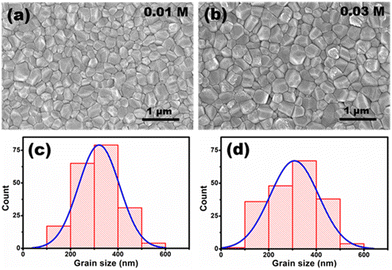
The SEM images of the perovskite films fabricated on [TMPA][TFSI] modified TiO2 compact layers are presented in Fig. 4(a) and (b). The films are homogeneous and do not contain pinholes. It is observed that the perovskite grain size is reduced upon application of [TMPA][TFSI] on the TiO2 surface. The average grain size in the control sample is approx. 400 nm (Fig. 1(a)), whereas it is approx. 320 nm in the [TMPA][TFSI] modified samples. Although the average grain size is reduced (hence, the grain count is increased) in the modified samples, the grain size distribution is narrower in the [TMPA][TFSI] modified samples (Fig. 4(c) and (d)) compared to the control sample (Fig. 1(d)). Furthermore, perovskite films are examined by optical microscopy immediately after dripping the antisolvent without annealing. It is observed that the nucleation and initial growth of the perovskite films are uniform in all cases (Fig. S7, ESI†). The narrow grain size distribution in the [TMPA][TFSI] modified films makes those films compact.54
The increased grain count and narrow distribution of the grain sizes suggest that the perovskite nucleation on the [TMPA][TFSI]-coated TiO2 compact layer is higher and uniform.55 The water contact angle of the TiO2 compact layers shows a decreasing trend upon application of [TMPA][TFSI] on its surface (Fig. S8, ESI†), i.e., the surface wettability of the TiO2 compact layer increases upon application of [TMPA][TFSI]. According to the classical theory of nucleation, the critical free energy, ΔG*, for homogeneous and heterogeneous nucleation are related as follows56
 | (1) |
The co-efficient Φ is related to the contact angle θ as follows
 | (2) |
Eqn (2) indicates that the smaller the contact angle θ (i.e., the higher the surface wettability), the lower the value of Φ, hence lowering the critical free energy for heterogeneous nucleation. So, upon application of [TMPA][TFSI], the energy barrier for nucleation is reduced as the surface wettability increases. This explains why nucleation numbers in [TMPA][TFSI] modified samples are higher and uniform.
The X-ray diffraction (XRD) patterns of the perovskite films fabricated on [TMPA][TFSI] modified TiO2 compact layers are shown in Fig. 5(a). The XRD patterns contain strong perovskite peaks without any impurity peaks of PbI2, which ensures complete conversion of the precursors and excellent crystal quality. The FWHM of the (001) peak is 0.288°, 0.293° and 0.291° for the 0 M, 0.01 M and 0.03 M samples, respectively, (Fig. S9, ESI†) indicating smaller crystallite size in [TMPA][TFSI] modified samples, which is supported by SEM images. However, it is observed that the ratio of the intensities of the (001) peak at 14.06° and the (111) peak at 24.58° is the highest in the 0.01 M sample and lowest in the 0 M sample. This indicates that surface modification with [TMPA][TFSI] ionic liquid leads to preferred crystal orientation in the (100) plane, which could lead to vertical grain growth.57 The UV-vis absorption spectroscopy of the perovskite films, shown in Fig. 5(b), indicates that the perovskite films fabricated on [TMPA][TFSI] modified TiO2 compact layers absorb more light than the perovskite film fabricated on the unmodified TiO2 compact layer, with the highest absorbance in the 0.01 M sample. The cross-section SEM images of the complete devices (Fig. S10, ESI†) show that the average thickness of the perovskite layers is approx. 620 nm. Therefore, the higher absorbance of the ionic liquid-modified perovskite films fabricated on modified TiO2 should be due to the higher compactness with a narrower grain size distribution of those films.
The TiO2/perovskite interface quality is characterized by steady-state PL (Fig. 5(c)). It is observed that the intensity of the PL spectra is drastically decreased upon application of [TMPA][TFSI] at the TiO2/perovskite interface, which indicates that the photogenerated electrons transfer more efficiently from the perovskite layer to the TiO2 layer due to the presence of [TMPA][TFSI] at the interface. Therefore, from the PL spectra, it can be inferred that a fine layer of [TMPA][TFSI] acts as a bridge and makes a robust contact between the TiO2 and perovskite layers. The presence of a fine layer of [TMPA][TFSI] on the TiO2 layer is confirmed by XPS (Fig. S11, ESI†). The XPS spectra of the unmodified TiO2 film contain peaks for Ti 2p at 457 eV and O 1s at 529 eV. On the other hand, the XPS spectra of the [TMPA][TFSI] modified TiO2 film contain the peaks for N 1s at 401 eV and F 1s at 687 eV, in addition to the peaks for Ti 2p and O 1s. The peaks for N 1s and F 1s confirm the presence of a fine layer of [TMPA][TFSI], as N is present in both the ions and F is present in the anion of [TMPA][TFSI]. The chemical structure of [TMPA][TFSI] is presented in Fig. 6(a).
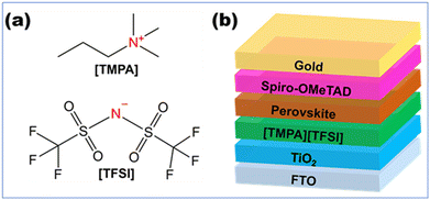 | ||
| Fig. 6 (a) Chemical structure and elemental composition of [TMPA][TFSI] ionic liquid. (b) Device architecture of [TMPA][TFSI] ionic liquid-modified PSCs. | ||
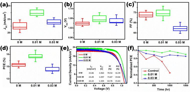
Perovskite solar cells are fabricated under ambient conditions with controlled humidity (25 ± 5% RH). It should be noted that for all the characterizations, the layers are deposited under the same conditions. The devices are fabricated with an architecture of FTO/TiO2/[TMPA][TFSI]/perovskite/spiro-OMeTAD/gold, illustrated in Fig. 6(b). At least seventeen devices are considered from each category to analyze the J–V data statistics. From the current–voltage (J–V) curves of the fabricated devices with various concentrations of [TMPA][TFSI], it can be seen that the JSC is enhanced in the [TMPA][TFSI] modified devices (Fig. 7(a)). The average JSC values of the 0 M, 0.01 M and 0.03 M devices are 20.96 ± 0.60 mA cm−2, 22.97 ± 0.42 mA cm−2 and 21.56 ± 0.43 mA cm−2, respectively. Therefore, 0.01 M devices showed the highest enhancement in JSC. The enhancement in the JSC is ascribed to the combined effect of higher light absorption by the perovskite layers and electron transfer efficiency at the TiO2/perovskite interfaces, evident from the UV-vis absorption spectroscopy and PL spectroscopy, respectively. Importantly, the VOC of the [TMPA][TFSI]-modified devices improved compared to that of unmodified devices (Fig. 7(b)). The average VOC values of the 0 M, 0.01 M and 0.03 M devices are 1.051 ± 0.014 V, 1.076 ± 0.022 V and 1.061 ± 0.071 V, respectively. Hence, 0.01 M devices show the most improvement in VOC. The improvement in VOC is attributed to the interfacial defect passivation by the constituent ions in the [TMPA][TFSI] ionic liquid, which is discussed later. The average FFs of the 0 M, 0.01 M and 0.03 M devices are 70.60 ± 1.65%, 71.48 ± 2.27% and 62.52 ± 1.76%, respectively (Fig. 7(c)). So, 0.01 M devices exhibit the highest average FF.
Due to the improvement in JSC, VOC, and FF, the 0.01 M devices achieved an average PCE of 17.51 ± 0.78%. The average PCEs of the 0 M and 0.03 M devices are 15.45 ± 0.49% and 14.31 ± 0.71%, respectively (Fig. 7(d)). The J–V curves of the best-performing devices of each type are presented in Fig. 7(e). The best PCEs achieved by the 0 M, 0.01 M and 0.03 M devices are 16.39%, 19.04% and 15.63%, respectively. Therefore, a modification with 0.01 M [TMPA][TFSI] ionic liquid at the TiO2/perovskite interface led to achieving an outstanding champion efficiency of 19.04%, fabricated under ambient conditions. The champion device achieved a JSC of 23.49 mA cm−2, VOC of 1.097 V, and FF of 73.87% (Table 2).
| J SC (mA cm−2) | V OC (V) | FF (%) | PCE (%) | ||
|---|---|---|---|---|---|
| 0 M | Avg. | 20.96 ± 0.60 | 1.051 ± 0.014 | 70.60 ± 1.65 | 15.45 ± 0.49 |
| Best cell | 21.86 | 1.063 | 70.54 | 16.39 | |
| 0.01 M | Avg. | 22.97 ± 0.42 | 1.076 ± 0.022 | 71.48 ± 2.27 | 17.51 ± 0.78 |
| Best cell | 23.49 | 1.097 | 73.87 | 19.04 | |
| 0.03 M | Avg. | 21.56 ± 0.43 | 1.061 ± 0.071 | 62.52 ± 1.76 | 14.31 ± 0.71 |
| Best cell | 22.22 | 1.103 | 63.78 | 15.63 | |
The stability of the [TMPA][TFSI] ionic liquid-modified devices is tested and compared to the control devices. In this study, the control devices are those which are fabricated using room temperature chlorobenzene antisolvent (25 °C) and without any interfacial modification by [TMPA][TFSI] ionic liquid at the TiO2/perovskite interface. The devices are kept under ambient conditions in the dark without any encapsulation. The stability data for the optimized devices are collected with a periodic measurement after every 250 h of dark storage (Fig. 7(f)). It is observed that the 0.01 M and 0.03 M devices retained >90% and >85%, respectively, of the initial PCE even after 1500 h. On the other hand, the control device degraded rapidly and retained only 45% of the initial PCE after 1000 h.
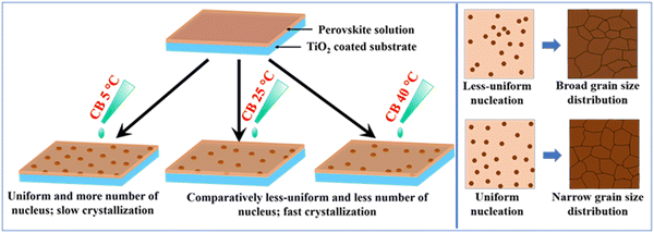
To understand better the effect of chlorobenzene temperature on crystallization and grain size distribution, we present a schematic in Fig. 8. At a lower temperature (5 °C), the nucleation numbers are higher and uniform. Whereas at a higher temperature (25 °C and 40 °C), the number of nucleations is comparatively low and less uniform. When the growth process takes place, the uniformly spaced nuclei grow into homogeneous grains. In the case of the less uniformly spaced nuclei, at the dense region, the nuclei get less space to grow and turn into smaller grains. On the other hand, in the sparse region, the nuclei get more space to grow and turn into large grains. These factors explain why low-temperature chlorobenzene leads to narrow and higher-temperature chlorobenzene leads to broad grain size distribution. Besides the homogeneous grain size, slow initial growth at low temperatures (5 °C) results in reduced defect density at the bulk and interface. Contrarily, at higher temperatures (25 °C and 40 °C), besides wider grain size distribution, initial grain growth happens at a faster rate, which leads to defects at the bulk and interfaces. The reduced defect density in the low-temperature antisolvent processed devices is reflected in their higher VOC and JSC.
Ren et al. also found a similar effect of antisolvent temperature. They observed, using in situ optical micrographs, that low-temperature (0 °C) antisolvent induces a larger number of nuclei with homogeneous spacing covering the whole substrate. After annealing, the substrate is covered with a compact perovskite film. On the other hand, high-temperature (30 °C) antisolvent leads to sporadic nucleation, which results in large grains with pinholes in the films. Utilizing diethyl ether and chlorobenzene antisolvents of 0 °C, they achieved the highest efficiency of 17.2% and 19.2%, respectively, in MAPbI3-based devices fabricated inside a glovebox. In comparison, diethyl ether and chlorobenzene antisolvents of 40 °C resulted in the highest efficiency of 14.3% and 13.8%, respectively.31
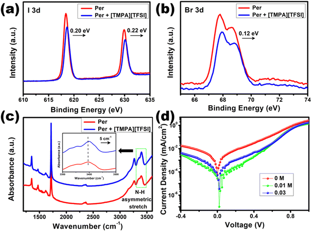
For an in-depth insight into the interaction between [TMPA][TFSI] and perovskite, [TMPA][TFSI] solution is coated on the perovskite layer and X-ray photoelectron spectroscopy (XPS) and Fourier transform infrared (FTIR) spectroscopy are done, then compared with the pristine samples. The XPS data revealed that the peaks for I 3d at 618.4 eV and 629.9 eV showed a shift of 0.20 eV and 0.22 eV, respectively, towards higher binding energy upon [TMPA][TFSI] modification (Fig. 9(a)). Similarly, the Br 3d peaks at 67.8 eV and 68.6 eV showed a shift of 0.12 eV towards higher binding energy in the modified sample (Fig. 9(b)). The peak shifts towards higher binding energy are attributed to the interaction between the [TMPA]+ cation of the ionic liquid and the uncoordinated I− and Br− anions of the perovskite.58 Hence, it is evident from the XPS that the [TMPA]+ cation passivates the Pb vacancies. Furthermore, the FTIR data revealed that the asymmetric stretching frequency of the N–H group (at 3395 cm−1), which is present in the FA (formamidinium) and MA (methylammonium) cations of the perovskite, shifts 5 cm−1 towards higher frequency (Fig. 9(c)). The frequency shift could be accredited to the hydrogen bond between the N–H group and [TFSI]− anion of the ionic liquid.59 Therefore, the FTIR data manifest that the [TFSI]− anion passivates the I− and Br− anion vacancies. So, from the XPS and FTIR data, it is elucidated that upon applying [TMPA][TFSI] ionic liquid at the TiO2/perovskite interface, various kinds of interfacial defects are effectively passivated.
Further evidence of interfacial defect passivation is obtained by dark J–V measurements (Fig. 9(d)). It is observed that the presence of [TMPA][TFSI] at the TiO2/perovskite interface reduces the dark current by more than one order. The decrease in dark current is due to the suppressed charge carrier recombination, which indicates the passivation of interfacial defects, resulting in improvement in VOC and JSC.60–62 To confirm the defect passivation by [TMPA][TFSI] ionic liquid, we performed SCLC measurements of the electron-only devices with the structure of FTO/TiO2/[TMPA][TFSI]/perovskite/LiF/Al and calculated the defect densities. The dark I–V plots of the electron-only devices are presented in Fig. S12 (ESI†). The trap-filled limit voltage (VTFL) is 0.75 V, 0.46 V and 0.50 V for 0 M, 0.01 M and 0.03 M [TMPA][TFSI] modification, respectively. The VTFL is correlated with defect density (nt) by the following relation:63
4. Conclusion
In conclusion, we developed highly efficient and stable triple-cation mixed halide based perovskite solar cells under ambient conditions by optimizing the chlorobenzene antisolvent temperature and applying [TMPA][TFSI] ionic liquid at TiO2/perovskite interface. Low-temperature chlorobenzene (5 °C) narrowed down the grain size distribution of the perovskite, leading to a compact film and better-quality interface, which enhanced the electron transfer. An optimum concentration of 0.01 M of [TMPA][TFSI] ionic liquid has resulted in a better-quality perovskite film with enhanced light absorbance, which increased the JSC. Importantly, improved interface quality and defect passivation at the interface led to improvement in VOC. The champion device achieved an excellent efficiency of 19.04% by modification with 0.01 M of [TMPA][TFSI] ionic liquid. Most significantly, the [TMPA][TFSI] ionic liquid-modified unencapsulated devices are highly stable with >90% PCE retention after 1500 h of storage in ambient conditions in the dark. This work pushes the effort toward the commercialization of perovskite solar cells one step further by demonstrating the fabrication of efficient and stable perovskite solar cells under ambient conditions.Author contributions
S. G. – conceptualization, data curation, formal analysis, investigation, writing – original draft; B. B. – investigation, visualization; S. P. – formal analysis, writing – review & editing; S. M. – formal analysis, visualization, writing – review & editing; T. S. – conceptualization, funding acquisition, supervision, writing – review & editing.Conflicts of interest
There are no conflicts of interest to declare.Acknowledgements
S. G., B. B. and S. M. are grateful to the Indian Institute of Technology Kharagpur for the fellowship and research facilities. S. P. acknowledges the Prime Minister Research Fellowship. T. S. acknowledges Science and Engineering Research Board (SRG/2019/1303 and IPA/2021/000081) for funding, and IIT Kharagpur for the research facilities. The authors acknowledge Trina Dhara for helping with contact angle measurements and Ankita Karmakar and Maruthi Manoj Brundavanam for PL measurements.References
- A. Kojima, K. Teshima, Y. Shirai and T. Miyasaka, J. Am. Chem. Soc., 2009, 131, 6050–6051 CrossRef CAS PubMed.
- J. M. Ball, M. M. Lee, A. Hey and H. J. Snaith, Energy Environ. Sci., 2013, 6, 1739–1743 RSC.
- F. Bella, G. Griffini, J.-P. Correa-Baena, G. Saracco, M. Grätzel, A. Hagfeldt, S. Turri and C. Gerbaldi, Science, 2016, 354, 203–206 CrossRef CAS PubMed.
- E. A. Alharbi, A. Krishna, T. P. Baumeler, M. Dankl, G. C. Fish, F. Eickemeyer, O. Ouellette, P. Ahlawat, V. Škorjanc, E. John, B. Yang, L. Pfeifer, C. E. Avalos, L. Pan, M. Mensi, P. A. Schouwink, J.-E. Moser, A. Hagfeldt, U. Rothlisberger, S. M. Zakeeruddin and M. Grätzel, ACS Energy Lett., 2021, 6, 3650–3660 CrossRef CAS.
- J. Jeong, M. Kim, J. Seo, H. Lu, P. Ahlawat, A. Mishra, Y. Yang, M. A. Hope, F. T. Eickemeyer, M. Kim, Y. J. Yoon, I. W. Choi, B. P. Darwich, S. J. Choi, Y. Jo, J. H. Lee, B. Walker, S. M. Zakeeruddin, L. Emsley, U. Rothlisberger, A. Hagfeldt, D. S. Kim, M. Grätzel and J. Y. Kim, Nature, 2021, 592, 381–385 CrossRef CAS PubMed.
- NREL, Best Research-Cell Efficiencies, (https://www.nrel.gov/pv/assets/pdfs/best-research-cell-efficiencies-rev220630.pdf).
- T. Singh, S. Öz, A. Sasinska, R. Frohnhoven, S. Mathur and T. Miyasaka, Adv. Funct. Mater., 2018, 28, 1706287 CrossRef.
- N.-G. Park, Mater. Today, 2015, 18, 65–72 CrossRef CAS.
- C. Liang, D. Zhao, P. Li, B. Wu, H. Gu, J. Zhang, T. W. Goh, S. Chen, Y. Chen, Z. Sha, G. Shao, T. C. Sum and G. Xing, Nano Energy, 2019, 59, 721–729 CrossRef CAS.
- S. D. Stranks, G. E. Eperon, G. Grancini, C. Menelaou, M. J. P. Alcocer, T. Leijtens, L. M. Herz, A. Petrozza and H. J. Snaith, Science, 2013, 342, 341–344 CrossRef CAS PubMed.
- M. Baranowski and P. Plochocka, Adv. Energy Mater., 2020, 10, 1903659 CrossRef CAS.
- Q. Lin, A. Armin, R. C. R. Nagiri, P. L. Burn and P. Meredith, Nat. Photonics, 2015, 9, 106–112 CrossRef CAS.
- L.-y Huang and W. R. L. Lambrecht, Phys. Rev. B: Condens. Matter Mater. Phys., 2013, 88, 165203 CrossRef.
- S. Mishra, S. Ghosh, B. Boro, D. Kumar, S. Porwal, M. Paul, H. Dixit and T. Singh, Energy Adv., 2022, 1, 761–792 RSC.
- B. Li, J. Tian, L. Guo, C. Fei, T. Shen, X. Qu and G. Cao, ACS Appl. Mater. Interfaces, 2016, 8, 4684–4690 CrossRef CAS PubMed.
- K. P. Marshall, M. Walker, R. I. Walton and R. A. Hatton, Nat. Energy, 2016, 1, 16178 CrossRef CAS.
- Y. Zhu, G. Lai, J. Yi, T. Zhang, Y. Zhang, S. Wen and H. Zhou, J. Alloys Compd., 2021, 866, 158990 CrossRef CAS.
- C. C. Boyd, R. Cheacharoen, T. Leijtens and M. D. McGehee, Chem. Rev., 2019, 119, 3418–3451 CrossRef CAS PubMed.
- N. Pant, A. Kulkarni, M. Yanagida, Y. Shirai, S. Yashiro, M. Sumiya, T. Miyasaka and K. Miyano, ACS Appl. Energy Mater., 2021, 4, 4530–4540 CrossRef CAS.
- A. Krishna, H. Zhang, Z. Zhou, T. Gallet, M. Dankl, O. Ouellette, F. T. Eickemeyer, F. Fu, S. Sanchez, M. Mensi, S. M. Zakeeruddin, U. Rothlisberger, G. N. Manjunatha Reddy, A. Redinger, M. Grätzel and A. Hagfeldt, Energy Environ. Sci., 2021, 14, 5552–5562 RSC.
- Z. Wan, H. Lai, S. Ren, R. He, Y. Jiang, J. Luo, Q. Chen, X. Hao, Y. Wang, J. Zhang, L. Wu and D. Zhao, J. Energy Chem., 2021, 57, 147–168 CrossRef CAS.
- S. Ghosh, S. Mishra and T. Singh, Adv. Mater. Interfaces, 2020, 7, 2000950 CrossRef CAS.
- M. Xiao, F. Huang, W. Huang, Y. Dkhissi, Y. Zhu, J. Etheridge, A. Gray-Weale, U. Bach, Y.-B. Cheng and L. Spiccia, Angew. Chem., Int. Ed., 2014, 53, 9898–9903 CrossRef CAS PubMed.
- J. W. Jung, S. T. Williams and A. K. Y. Jen, RSC Adv., 2014, 4, 62971–62977 RSC.
- X. Zheng, B. Chen, C. Wu and S. Priya, Nano Energy, 2015, 17, 269–278 CrossRef CAS.
- N. Ahn, D.-Y. Son, I.-H. Jang, S. M. Kang, M. Choi and N.-G. Park, J. Am. Chem. Soc., 2015, 137, 8696–8699 CrossRef CAS PubMed.
- M. Yavari, M. Mazloum-Ardakani, S. Gholipour, M. M. Tavakoli, S.-H. Turren-Cruz, N. Taghavinia, M. Grätzel, A. Hagfeldt and M. Saliba, Adv. Energy Mater., 2018, 8, 1800177 CrossRef.
- J. Troughton, K. Hooper and T. M. Watson, Nano Energy, 2017, 39, 60–68 CrossRef CAS.
- N. J. Jeon, J. H. Noh, Y. C. Kim, W. S. Yang, S. Ryu and S. I. Seok, Nat. Mater., 2014, 13, 897–903 CrossRef CAS PubMed.
- T. Singh and T. Miyasaka, Adv. Energy Mater., 2018, 8, 1700677 CrossRef.
- Y.-K. Ren, X.-H. Ding, Y.-H. Wu, J. Zhu, T. Hayat, A. Alsaedi, Y.-F. Xu, Z.-Q. Li, S.-F. Yang and S.-Y. Dai, J. Mater. Chem. A, 2017, 5, 20327–20333 RSC.
- H. Taherianfard, G.-W. Kim, M. M. Byranvand, K. Choi, G. Kang, H. Choi, F. Tajabadi, N. Taghavinia and T. Park, ACS Appl. Energy Mater., 2020, 3, 1506–1514 CrossRef CAS.
- S. Ghosh and T. Singh, Nano Energy, 2019, 63, 103828 CrossRef CAS.
- M. Shahiduzzaman, E. Y. Muslih, A. K. M. Hasan, L. Wang, S. Fukaya, M. Nakano, M. Karakawa, K. Takahashi, M. Akhtaruzzaman, J.-M. Nunzi and T. Taima, Chem. Eng. J., 2021, 411, 128461 CrossRef CAS.
- H. Wu, Z. Li, F. Zhang, C. Kang and Y. Li, Adv. Mater. Interfaces, 2022, 2201292 CrossRef CAS.
- D. Yang, X. Zhou, R. Yang, Z. Yang, W. Yu, X. Wang, C. Li, S. Liu and R. P. H. Chang, Energy Environ. Sci., 2016, 9, 3071–3078 RSC.
- W. Zhang, Z. Ren, Y. Guo, X. He and X. Li, Electrochim. Acta, 2018, 268, 539–545 CrossRef CAS.
- N. K. Noel, S. N. Habisreutinger, B. Wenger, Y.-H. Lin, F. Zhang, J. B. Patel, A. Kahn, M. B. Johnston and H. J. Snaith, Adv. Energy Mater., 2020, 10, 1903231 CrossRef CAS.
- W. Zhang, X. Liu, B. He, Z. Gong, J. Zhu, Y. Ding, H. Chen and Q. Tang, ACS Appl. Mater. Interfaces, 2020, 12, 4540–4548 CrossRef CAS PubMed.
- X. Zhu, M. Du, J. Feng, H. Wang, Z. Xu, L. Wang, S. Zuo, C. Wang, Z. Wang, C. Zhang, X. Ren, S. Priya, D. Yang and S. Liu, Angew. Chem., Int. Ed., 2021, 60, 4238–4244 CrossRef CAS PubMed.
- W. Hou, Y. Ma, J. Kang, Y. Xiao and G. Han, Adv. Mater. Interfaces, 2022, 2201259 CrossRef CAS.
- P. Wasserscheid and T. Welton, Ionic Liquids in Synthesis, Wiley-VCH, 2007 Search PubMed.
- S. Cuadrado-Prado, M. Domínguez-Pérez, E. Rilo, S. García-Garabal, L. Segade, C. Franjo and O. Cabeza, Fluid Phase Equilib., 2009, 278, 36–40 CrossRef CAS.
- Y. Guo, L. Kang, M. Zhu, Y. Zhang, X. Li and P. Xu, Chem. Eng. J., 2018, 336, 732–740 CrossRef CAS.
- K. Huang, H. Li, C. Zhang, Y. Gao, T. Liu, J. Zhang, Y. Gao, Y. Peng, L. Ding and J. Yang, Sol. RRL, 2019, 3, 1800318 CrossRef.
- S. Ghosh and T. Singh, Mater. Lett., 2022, 322, 132490 CrossRef CAS.
- L. Gao, K. Huang, C. Long, F. Zeng, B. Liu and J. Yang, Appl. Phys. A: Mater. Sci. Process., 2020, 126, 452 CrossRef CAS.
- Y. Zhang, A. Kirs, F. Ambroz, C.-T. Lin, A. S. R. Bati, I. P. Parkin, J. G. Shapter, M. Batmunkh and T. J. Macdonald, Small Methods, 2021, 5, 2000744 CrossRef CAS PubMed.
- K. Liu, P. W. K. Fong, Q. Liang and G. Li, Trends Chem., 2021, 3, 747–764 CrossRef CAS.
- X. Duan, X. Li, L. Tan, Z. Huang, J. Yang, G. Liu, Z. Lin and Y. Chen, Adv. Mater., 2020, 32, 2000617 CrossRef CAS PubMed.
- B. Wu, K. Fu, N. Yantara, G. Xing, S. Sun, T. C. Sum and N. Mathews, Adv. Energy Mater., 2015, 5, 1500829 CrossRef.
- H. Li, X. Jiang, Q. Wei, Z. Zang, M. Ma, F. Wang, W. Zhou and Z. J. A. C. Ning, Angew. Chem., Int. Ed., 2021, 133, 16466–16472 CrossRef.
- R. D. Chavan, M. Wolska-Pietkiewicz, D. Prochowicz, M. Jędrzejewska, M. M. Tavakoli, P. Yadav, C. K. Hong and J. Lewiński, Adv. Funct. Mater., 2022, 32, 2205909 CrossRef CAS.
- W.-Q. Wu, Z. Yang, P. N. Rudd, Y. Shao, X. Dai, H. Wei, J. Zhao, Y. Fang, Q. Wang, Y. Liu, Y. Deng, X. Xiao, Y. Feng and J. Huang, Sci. Adv., 2019, 5(3), eaav8925 CrossRef CAS PubMed.
- N. Tripathi, Y. Shirai, M. Yanagida, A. Karen and K. Miyano, ACS Appl. Mater. Interfaces, 2016, 8, 4644–4650 CrossRef CAS PubMed.
- H. Hu, M. Singh, X. Wan, J. Tang, C.-W. Chu and G. Li, J. Mater. Chem. A, 2020, 8, 1578–1603 RSC.
- G. Tang, P. You, Q. Tai, A. Yang, J. Cao, F. Zheng, Z. Zhou, J. Zhao, P. K. L. Chan and F. Yan, Adv. Mater., 2019, 31, 1807689 CrossRef PubMed.
- Z. Huang, X. Hu, C. Liu, L. Tan and Y. Chen, Adv. Funct. Mater., 2017, 27, 1703061 CrossRef.
- A. Sharma and N. B. Chaure, Appl. Phys. A: Mater. Sci. Process., 2019, 125, 767 CrossRef.
- P. Guo, Q. Ye, C. Liu, F. Cao, X. Yang, L. Ye, W. Zhao, H. Wang, L. Li and H. Wang, Adv. Funct. Mater., 2020, 30, 2002639 CrossRef CAS.
- H. Wang, Z. Wang, Z. Yang, Y. Xu, Y. Ding, L. Tan, C. Yi, Z. Zhang, K. Meng, G. Chen, Y. Zhao, Y. Luo, X. Zhang, A. Hagfeldt and J. Luo, Adv. Mater., 2020, 32, 2000865 CrossRef CAS PubMed.
- M. A. R. Laskar, W. Luo, N. Ghimire, A. H. Chowdhury, B. Bahrami, A. Gurung, K. M. Reza, R. Pathak, R. S. Bobba, B. S. Lamsal, K. Chen, M. T. Rahman, S. I. Rahman, K. Emshadi, T. Xu, M. Liang, W.-H. Zhang and Q. Qiao, Adv. Funct. Mater., 2020, 30, 2000778 CrossRef CAS.
- S. Wang, Z. Li, Y. Zhang, X. Liu, J. Han, X. Li, Z. Liu, S. Liu and W. C. H. Choy, Adv. Funct. Mater., 2019, 29, 1900417 CrossRef.
Footnote |
| † Electronic supplementary information (ESI) available. See DOI: https://doi.org/10.1039/d3ya00065f |
| This journal is © The Royal Society of Chemistry 2023 |

