
Reversible photoluminescence modulation of monolayer MoS2 on a ferroelectric substrate by light irradiation and thermal annealing†
Peng
Wang
ab,
Jian
Wang
a,
Yun
Zheng
a,
Hongyan
Shi
ac,
Xiudong
Sun
ac,
Wenjun
Liu
b and
Bo
Gao
 *ac
*ac
aInstitute of Modern Optics, School of Physics, Key Laboratory of Micro-Nano Optoelectronic Information System, Ministry of Industry and Information Technology, Key Laboratory of Micro-Optics and Photonic Technology of Heilongjiang Province, Harbin Institute of Technology, Harbin 150001, China. E-mail: gaobo@hit.edu.cn
bDepartment of Physics, Harbin Institute of Technology at Weihai, Weihai 264209, China
cCollaborative Innovation Center of Extreme Optics, Shanxi University, Taiyuan 030006, China
First published on 15th July 2021
Abstract
Monolayer semiconducting two-dimensional (2D) materials are strongly emerging materials for exploring the spin-valley coupling effect and fabricating novel optoelectronic devices due to their unique structural symmetry and band structures. Due to their atomic thickness, their excitonic optical response is highly sensitive to the dielectric environment. In this work, we present a novel approach to reversibly modulate the optical properties of monolayer molybdenum disulfide (MoS2) via changing the dielectric properties of the substrate by laser irradiation and thermal annealing. We chose LiNbO3 as the substrate and recorded the PL spectra of monolayer MoS2 on LiNbO3 substrates with positive (P+) and negative (P−) ferroelectric polarities. A distinct PL intensity of the A peak was observed due to opposite doping by surface charges. Under light irradiation, the PL intensity of monolayer MoS2 on P+ Fe2O3-doped LiNbO3 gradually decreased with time due to the reduction of intrinsic p-doping, which originated from the drift of photo-excited electrons under a spontaneous polarization field and accumulation on the surface. The PL intensity was found to be restored by thermal annealing which could erase the charge redistribution. This study provides a strategy to reversibly modulate the optical properties of monolayer 2D materials on top of ferroelectric materials.
1. Introduction
Two-dimensional (2D) materials have attracted intense research interest both in theory and experiment due to their fascinating crystal lattice structures and electronic properties in the past few decades. Layered transition metal dichalcogenides (TMDs), which are semiconductors with a chemical formula MX2 (M = Mo, W, etc.; X = S, Se, Te), have been extensively investigated owing to their unique electrical and optical properties.1–7 In particular, monolayer TMDs, whose band structure evolves from indirect gap to direct gap, produce a strong exciton pumping efficiency with energy gaps located at the Brillouin zone owing to the atomically thin structure.8–11 Monolayer TMDs provide a platform for investigating tightly bound excitonic states, spin-valley coupling, optically controlled valley polarization and coherence,12–17 and hence are regarded as a promising class of materials for next-generation state-of-art micro/nano optoelectronic devices. It is usually essential to modify and modulate the electronic, chemical and optical properties of 2D materials for a wide range of applications in flexible electronics,18–20 gas sensors,21 transistors10 and biosensors.22 So far, many strategies have been developed to modulate the optical properties of 2D materials, including chemical doping, electrostatic gating and structuring. In the case of electrostatic gating, a field-effect transistor (FET) configuration was usually employed to reversibly regulate the number of charge carriers in 2D materials.23–26 However, the metal gates require additional processing steps and result in inhomogeneous spatial distribution of charge carriers,27,28 and the metallic contact with TMDs could quench the light emission at the interface. To overcome these disadvantages, many other novel methods have been put forward to modulate the charge transport and optical properties of 2D TMDs, such as light irradiation, substrate induction, or environment assistance.Due to the pronounced photorefractive, pyroelectric and piezoelectric properties, lithium niobate (LiNbO3) has been used in electro-optical modulators, surface acoustic wave devices, piezoelectric sensors and holographic recording.29–31 It is unfortunate that LiNbO3 is a wide-gap insulator which limits its application in optoelectronics. Recently, the concept of integrating LiNbO3 and semiconductor materials has been proposed.30,31 By transferring monolayer MoSe2 and WSe2 onto the surface of domain-engineered LiNbO3, their photoluminescence (PL) was significantly enhanced or inhibited,32 because reversible and nonvolatile control of TMD doping was induced by opposite surface charges on the LiNbO3 substrate with different domain orientations. It is known that local light irradiation could redistribute the space charge in LiNbO3 due to the migration and stable trapping of photo-excited electrons,33 which could change its dielectric properties and may affect the charge transport and optical properties of 2D TMDs on top. It is also reported that the trapped electrons could be re-activated and the charge distribution could be restored by thermal annealing34–37 or uniform UV light irradiation,38 which might have an opposite effect on 2D TMDs to light irradiation. Therefore, it is possible to reversibly modulate the optical properties of 2D TMDs on LiNbO3 by combining light irradiation and thermal annealing, which are nondestructive and noncontact techniques.
In this work, we present a novel approach to reversibly modulate the optical properties of monolayer MoS2via changing the dielectric properties of the substrate by laser irradiation and thermal annealing. Our approach is based on LiNbO3, a widely known ferroelectric material for various optical and acoustic applications. Due to the inherent surface charges, the polarized LiNbO3 was found to change the doping and hence the PL of the supported monolayer MoS2. After that, using laser we irradiated Fe2O3-doped LiNbO3 with a positive ferroelectric polarity to excite and accumulate electrons on the surface under a spontaneous polarization field, and found that the PL intensity of the A peak of the supporting monolayer MoS2 decreased with irradiation time. After thermally annealing the irradiated sample to erase the charge redistribution, the PL intensity of the A peak was restored. This study demonstrated a reversible PL modulation of monolayer 2D materials by optically irradiating and thermally annealing the beneath ferroelectric substrates.
2. Experimental
2.1 CVD growth of monolayer MoS2 on SiO2/Si
Monolayer MoS2 was grown on SiO2/Si substrates with 300 nm of SiO2 by chemical vapor deposition (CVD). Briefly, solid state precursors of MoO3 and sulfur powder were loaded into a 1-inch quartz tube with a distance of 18 cm. A firebrick crucible filled with sulfur powder was placed upstream in the quartz tube outside the furnace, and an alumina crucible filled with MoO3 powder was loaded in the center of the furnace. The sulfur vapor was introduced by Ar to react with molybdenum oxide (MoOx from MoO3) at an elevated temperature (660 °C) for monolayer MoS2 growth by sulfurization reactions. In order to acquire large-size monolayer MoS2 with high quality, we used traces of alkali metal compounds as promoters to facilitate the growth. Monolayer WS2 was synthesized at 850 °C by using solid WO3 and S precursors.2.2 Transfer of monolayer MoS2 onto a ferroelectric substrate
To avoid possible contamination, freshly made PDMS was used for transferring monolayer MoS2 from SiO2/Si onto a LiNbO3 substrate, as schematically shown in Fig. 1a. A piece of PDMS was attached onto the MoS2-covered SiO2/Si surface and was immersed into deionized (DI) water. Then, the PDMS, adhering MoS2, was gently peeled from the SiO2/Si surface. Subsequently, the MoS2-covered PDMS was taken out of DI water and attached onto the LiNbO3 surface. After baking in a vacuum oven at 60 °C for 5 min, the PDMS was peeled from the LiNbO3 surface, leaving MoS2 on the LiNbO3 substrate. To eliminate the possible variance of different batches of CVD-grown MoS2 on SiO2/Si, the as-grown sample was sliced into several parts and separately transferred onto different substrates. The control experiment involving the transfer onto the hydrophilic SiO2/Si substrate shows that the morphology and optical properties of MoS2 could be well preserved (Fig. S1, ESI†).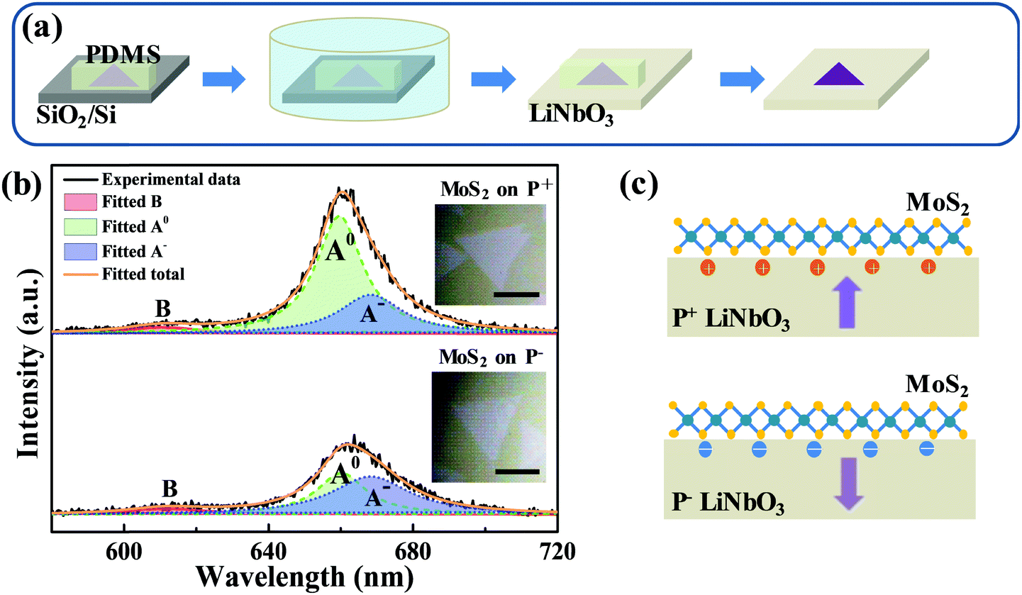 | ||
| Fig. 1 (a) Schematic illustration of the PDMS-assisted transfer process developed in this work. (b) Micro-PL spectra of monolayer MoS2 on LiNbO3 with positive ferroelectric polarity (P+) and negative polarity (P−). The dotted lines show the fitted peaks. Insets show the corresponding optical images of the monolayer MoS2. Scale bars: 25 μm. (c) Schematic illustration of the induced surface charges and the expected doping effect on monolayer MoS2. Purple arrows depict the polarized orientation of the LiNbO3 substrate. | ||
2.3 Characterization
A continuous wave 532 nm laser with a power of 40 μW and a spot size of ∼1 μm was used for long-time illumination to form charge redistribution. Thermal annealing was carried out in a heating/cooling stage (HCS321Gi, INSTEC Inc.) to restore the LiNbO3 substrate to uniform charge distribution. Micro-Raman and -PL spectra were collected to characterize the optical properties of monolayer MoS2 and WS2 on various substrates (NT-MDT NTEGRA Spectra). The morphology of monolayer MoS2 and WS2 on LiNbO3 was characterized by optical microscopy (OLYMPUS BX51).3. Results and discussion
The as-grown monolayer MoS2 has uniform light emission (Fig. S2, ESI†), providing an excellent prototype for this study. Fig. 1b shows the typical PL spectra of monolayer MoS2 on z-cut LiNbO3 substrates with positive (P+) and negative (P−) ferroelectric polarities, which were recorded under a pump power of 40 μW to avoid any heating and oxidation effects. The insets show the optical images. Both samples exhibit a clean surface and well-known A and B peaks, confirming the high quality of transferred monolayer MoS2. But the PL intensity of the A peak from monolayer MoS2 on the P+ LiNbO3 substrate was enhanced, while on the P− LiNbO3 substrate the PL intensity of the A peak was suppressed. The PL intensity of the B peak had no differences between the two samples. To clearly show the spectral differences, the A peak in the PL spectra was fitted by two Lorentzian peaks corresponding to neural exciton (A0) and trion exciton (A−), respectively (Fig. 1b). It can be seen that the PL intensity of A0 on the P+ substrate was much larger than that on the P− substrate, while the PL intensity of A− did not change, resulting in a larger PL intensity ratio between A− and A on the P− substrate. This, along with the distinct A peak intensity, indicates more p-type doping on the P+ substrate and more n-type doping on the P− substrate, which are due to the distinct dielectric environment of the LiNbO3 surface originating from the polarized state.32Fig. 1c schematically shows the LiNbO3-induced doping effect on monolayer MoS2. The P+ LiNbO3 substrate has an up-polarized state, in which the positive surface charges accumulate and enhance the intrinsic p-type character of MoS2.39,40 In contrast, the P− LiNbO3 substrate has a down-polarized state, resulting in rich negative surface charges and hence n-type doping of monolayer MoS2. The distinct p- and n-type doping would enhance and suppress the PL emission, respectively. Due to the unfortunate overlap of vibrational modes of MoS2 and LiNbO3, Raman spectroscopy, which is also an easy indicator for doping of monolayer MoS2, could not be used in this work.As a photorefractive material, light irradiation is believed to produce space charge distribution in LiNbO3 due to the migration and stable trapping of photo-excited electrons, providing the possibility of modulating the optical properties of the supporting MoS2. Fig. 2a and b show the PL spectra of monolayer MoS2 on P+ and P− LiNbO3 substrates for laser irradiation time up to 9 min. It can be seen that the PL intensity remains nearly constant with the laser irradiation time for both P+ and P− LiNbO3 substrates, which is possibly due to the low optical response of pure LiNbO3.34,41,42
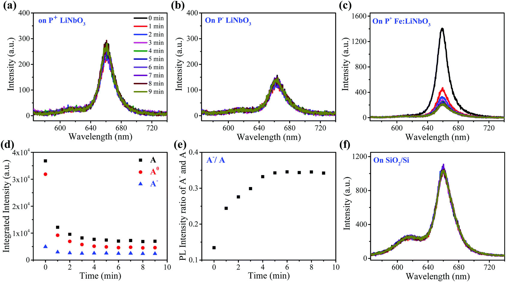 | ||
| Fig. 2 PL spectra of monolayer MoS2 on (a) P+ LiNbO3, (b) P− LiNbO3 and (c) P+ Fe:LiNbO3 for laser irradiation time up to 9 min, respectively. (d) Integrated PL intensity of A0, A− and A peaks and (e) PL intensity ratio of A− and A from monolayer MoS2 on P+ Fe:LiNbO3 as a function of laser irradiation time. (f) PL spectra of monolayer MoS2 on SiO2/Si for laser irradiation time up to 9 min. | ||
In order to enhance the optical response of LiNbO3 for the modulation of the optical properties of MoS2, we used z-cut Fe2O3-doped LiNbO3 with a positive ferroelectric polarity (P+ Fe:LiNbO3) as the substrate. Fig. 2c shows the PL spectra of monolayer MoS2 on the P+ Fe:LiNbO3 substrate for laser irradiation time up to 9 min. The PL intensity of monolayer MoS2 was much larger than that on undoped LiNbO3 due to the presence of Fe ions. After laser irradiation, the PL intensity of the B peak had no obvious changes, while the PL intensity of the A peak changed. To clearly show the variation tendency, the PL spectra were fitted. Fig. 2d shows the integrated intensity of A0, A− and A peaks as a function of laser irradiation time, all of which have similar tendency. In the first 1 min, the PL intensity of the A peak decreased sharply. Within subsequent 2–4 min, the PL intensity slightly decreased. After 4 min, the intensity remained almost constant. Besides, we plotted the intensity ratio of A− and A peaks as a function of laser irradiation time, which was found to increase (Fig. 2e). The decrease of the intensity and the increase of the intensity ratio with irradiation time are similar to the change of the A peak when employing a gate voltage43,44 and functionalizing MoS2 with n-type molecules.40,45 We also recorded the PL spectra of monolayer MoS2 on the SiO2/Si substrate as a function of irradiation time as a control experiment. It can be seen that the PL intensity remained nearly constant as the irradiation time increased, indicating that the Fe:LiNbO3 substrate played a vital role in the PL change.
The PL change of monolayer MoS2 on P+ Fe:LiNbO3 as a function of laser irradiation time was attributed to the modulation of the surrounding dielectric environment, as schematically shown in Fig. 3. The doped Fe ions in Fe:LiNbO3 have two valence states, Fe2+ and Fe3+, which act as photo-excited charge centers to produce electrons or holes under light irradiation, and govern the migration of free photo-excited electrons according to the following scheme:34
| Fe2+ + hν → Fe3+ + e | (1) |
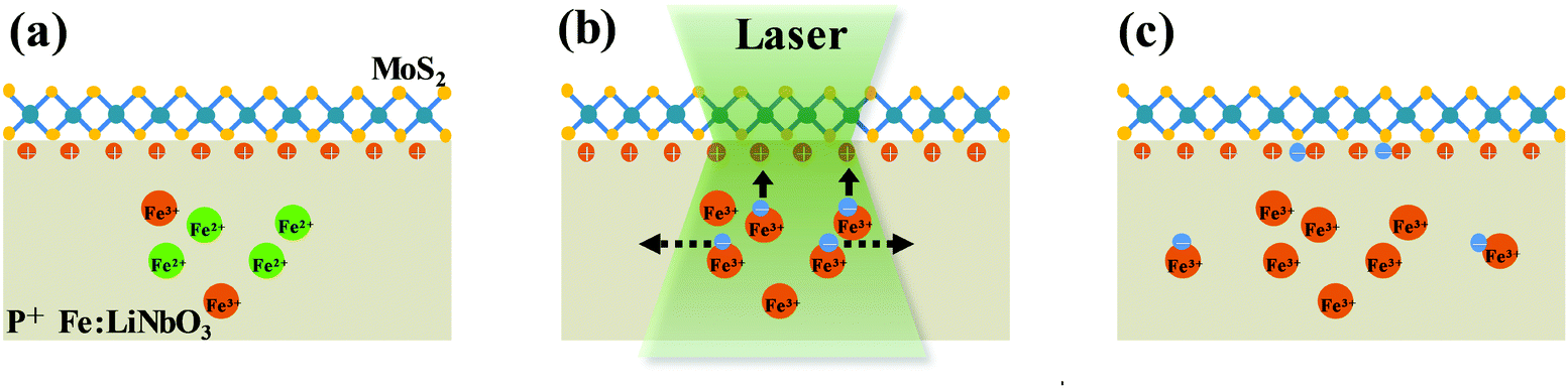 | ||
| Fig. 3 Schematic illustration of the dielectric environment of monolayer MoS2 on P+ Fe:LiNbO3 under laser irradiation. (a) Positive ferroelectric polarity and its induced surface charge. (b) Drift and diffusion of the excited electrons. The solid arrows depict the drift effect of photo-excited electrons under a spontaneous polarization field, while the dotted arrows depict the diffusion due to the concentration gradient. (c) The electrons arriving at the positive surface of P+ Fe:LiNbO3 reduce the initial doping effect of MoS2 produced by polarized surface charges. | ||
Due to the lower valence state, Fe2+ impurity sites can act as donors to supply electrons to the conduction band. The photo-excited electrons migrate freely in the lattice. Two main effects dominate the migration: the spontaneous polarization field and concentration gradient of free electrons. The former originates from the asymmetry of the crystalline structure of LiNbO3, which results in a spontaneous polar moment. The orientation of the polar moment of each cell in a polarized ferroelectric crystal is consistent, which is equivalent to an internal electric field. As shown by the solid arrows in Fig. 3b, the photo-generated electrons drift under the action of the electric field, which is also named photovoltaic effect. The latter originates from the concentration gradient of free electrons between the irradiation area and the dark region in the LiNbO3 crystal.46 As shown by the dotted arrows in Fig. 3b, photo-excited electrons diffuse away from the irradiation area to the dark region, and get trapped by acceptor sites of Fe3+. The scheme of this capture process can be interpreted as follows:
| Fe3+ + e → Fe2+ | (2) |
The drift of the excited electrons redefines the local dielectric environment at the surface of LiNbO3.
Most notably, the areal charge density of the positive z-cut face of LiNbO3 can reach as large as σz = 0.7 C m−2 due to its spontaneous polarization, producing a large internal electric field. Excited electrons prefer to be controlled by the electric field rather than diffusing away. When the electrons arrive at the positive surface of P+ Fe:LiNbO3, the initial doping effect of MoS2 by polarized surface charge will be reduced, resulting in the modulation of PL emission. However, the concentration of the dopant limits the number of excited electrons in LiNbO3. As the irradiation time increased, the concentration of photo-excited electrons gradually decreased until it reached the limit.47,48 Under the experimental conditions in this work, the drift of photo-excited electrons to the surface was mainly achieved in the first 1 min, decreasing the PL intensity of MoS2 sharply. In the subsequent 2–4 min, the doping effect gradually became insensitive to laser illumination time as the concentration of photo-excited electrons decreased. After 4 min, the PL intensity of MoS2 remained almost constant due to the complete depletion of Fe2+ ions which is responsible for the redistribution of the surface charge. In pure LiNbO3, due to the low density of excited electrons, few charge carriers were optically excited and no PL modulation could be observed.
It is known that the resulting charge redistribution, existing for a long period due to the deep trap state, could be erased by thermal annealing34–37 or uniform UV light irradiation.38 In order to avoid possible damage to MoS2 by UV light,49 we chose thermal annealing to erase the charge redistribution, which was performed in a heating/cooling stage at 150 °C for 20 min in argon to restore P+ Fe:LiNbO3 to the initial state. The heating/cooling stage was placed on a home-built confocal microscope for in situ PL measurement. Fig. 4a shows the PL spectra of monolayer MoS2 on P+ Fe:LiNbO3 before laser irradiation (black curve), after laser irradiation (blue curve) and after thermal annealing (red curve). Similar to those in Fig. 3, the PL intensity decreased after laser irradiation for 9 min. But subsequent thermal annealing restored the PL intensity. Fig. 4b schematically illustrates the erasing of charge redistribution in P+ Fe:LiNbO3via thermal annealing. The electrons on the surface are activated by heating, and then diffuse at high temperatures until captured by Fe3+. In the meantime, the heating provides the activation energy to excite the electronic charge in Fe3+ traps, which diffused back to the light irradiation area.35,48 The overall effect is the erasing of charge redistribution produced by light irradiation. Therein, the migration of the surface electrons and hence recovery of the surface charge states lead to the restoration of the PL intensity. In order to explore the reversibility over time, we performed laser illumination and thermal annealing for another four cycles. It can be seen that the reversible PL modulation could be well achieved after five cycles, suggesting long-time reversibility.
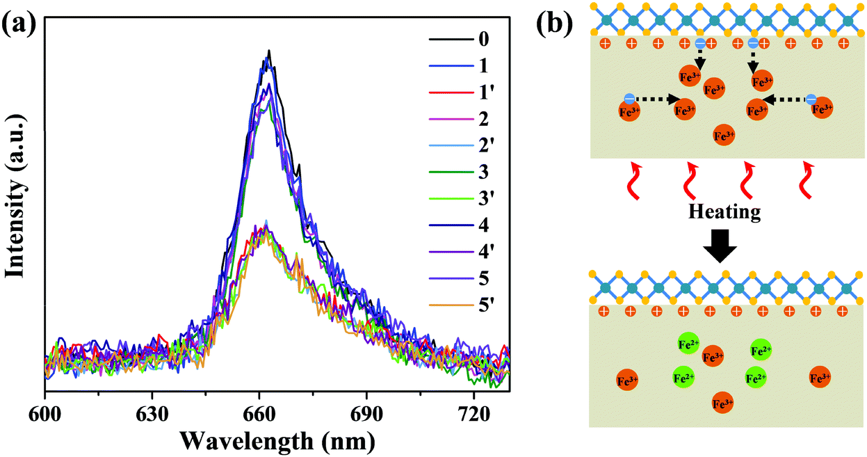 | ||
| Fig. 4 (a) Reversible modulation of PL intensity for 5 cycles by laser irradiation and thermal annealing. (0) PL spectra of monolayer MoS2 on P+ Fe:LiNbO3 before laser irradiation. (1–5) PL spectra after laser irradiation and (1′–5′) restored PL spectra after thermal annealing. (b) Schematic illustration of erasing the charge redistribution in P+ Fe:LiNbO3via thermal annealing. | ||
Besides, we carried out experiments using CVD-grown monolayer WS2, and reversible PL modulation was also achieved for monolayer WS2 on the P+ Fe:LiNbO3 substrate by light irradiation and thermal annealing (Fig. S3, ESI†), suggesting that the reversible modulation strategy could be universally extended to other 2D materials.
4. Conclusions
In this work, we have successfully achieved PL modulation in monolayer MoS2 by light irradiation and thermal annealing by using a ferroelectric LiNbO3 substrate. The PL intensity of the A peak of monolayer MoS2 was enhanced/suppressed due to the p-/n-doping by the positive/negative polarized charge on the P+/P− LiNbO3 substrate. Under light irradiation, the PL intensity of the A peak of monolayer MoS2 on the P+ Fe:LiNbO3 substrate gradually decreased with time, and was restored after thermal annealing. This change is due to the reduction and the recovery of intrinsic p-doping of monolayer MoS2, which originated from the light-induced redistribution and heat-activated recovery of the surface charge. This study provides a strategy to reversibly modulate the optical properties of monolayer 2D materials on top of ferroelectric materials, which could have a great potential application in the fields of information encryption, data storage and memory chips.Author contributions
B. G. initiated the idea. P. W. and H. S. did the experiment. All authors analyzed and interpreted the data. P. W. and B. G. wrote the manuscript. B. G. supervised the project.Conflicts of interest
The authors declare no competing financial interest.Acknowledgements
This work was financially supported by the National Natural Science Foundation of China. (No. 91956129 and 21973023).Notes and references
- H. Li, J. Wu, Z. Yin and H. Zhang, Acc. Chem. Res., 2014, 47, 1067–1075 CrossRef CAS.
- Z. Cai, B. Liu, X. Zou and H.-M. Cheng, Chem. Rev., 2018, 118, 6091–6133 CrossRef CAS PubMed.
- Y. Chen, Z. Fan, Z. Zhang, W. Niu, C. Li, N. Yang, B. Chen and H. Zhang, Chem. Rev., 2018, 118, 6409–6455 CrossRef CAS.
- M. Chhowalla, H. S. Shin, G. Eda, L.-J. Li, K. P. Loh and H. Zhang, Nat. Chem., 2013, 5, 263–275 CrossRef.
- X. Yu, M. S. Prévot, N. Guijarro and K. Sivula, Nat. Commun., 2015, 6, 7596 CrossRef PubMed.
- O. Lopez-Sanchez, D. Lembke, M. Kayci, A. Radenovic and A. Kis, Nat. Nanotechnol., 2013, 8, 497–501 CrossRef CAS PubMed.
- A. Castellanos-Gomez, Nat. Photonics, 2016, 10, 202–204 CrossRef CAS.
- M. Buscema, J. O. Island, D. J. Groenendijk, S. I. Blanter, G. A. Steele, H. S. J. van der Zant and A. Castellanos-Gomez, Chem. Soc. Rev., 2015, 44, 3691–3718 RSC.
- S. Tongay, J. Zhou, C. Ataca, J. Liu, J. S. Kang, T. S. Matthews, L. You, J. Li, J. C. Grossman and J. Wu, Nano Lett., 2013, 13, 2831–2836 CrossRef CAS PubMed.
- B. Radisavljevic, A. Radenovic, J. Brivio, V. Giacometti and A. Kis, Nat. Nanotechnol., 2011, 6, 147–150 CrossRef CAS PubMed.
- K. F. Mak and J. Shan, Nat. Photonics, 2016, 10, 216–226 CrossRef CAS.
- A. Splendiani, L. Sun, Y. Zhang, T. Li, J. Kim, C. Y. Chim, G. Galli and F. Wang, Nano Lett., 2010, 10, 1271–1275 CrossRef CAS PubMed.
- Y. Zhang, T.-R. Chang, B. Zhou, Y.-T. Cui, H. Yan, Z. Liu, F. Schmitt, J. Lee, R. Moore, Y. Chen, H. Lin, H.-T. Jeng, S.-K. Mo, Z. Hussain, A. Bansil and Z.-X. Shen, Nat. Nanotechnol., 2014, 9, 111–115 CrossRef CAS.
- F. Xia, H. Wang, D. Xiao, M. Dubey and A. Ramasubramaniam, Nat. Photonics, 2014, 8, 899–907 CrossRef CAS.
- A. F. Morpurgo, Nat. Phys., 2013, 9, 532–533 Search PubMed.
- Z. Ye, D. Sun and T. F. Heinz, Nat. Phys., 2017, 13, 26–29 Search PubMed.
- K. He, N. Kumar, L. Zhao, Z. Wang, K. F. Mak, H. Zhao and J. Shan, Phys. Rev. Lett., 2014, 113, 026803 CrossRef CAS PubMed.
- T.-Y. Wang, J.-L. Meng, Z.-Y. He, L. Chen, H. Zhu, Q.-Q. Sun, S.-J. Ding, P. Zhou and D. W. Zhang, Adv. Sci., 2020, 7, 1903480 CrossRef CAS.
- Q. Wang, N. Li, J. Tang, J. Zhu, Q. Zhang, Q. Jia, Y. Lu, Z. Wei, H. Yu, Y. Zhao, Y. Guo, L. Gu, G. Sun, W. Yang, R. Yang, D. Shi and G. Zhang, Nano Lett., 2020, 20, 7193–7199 CrossRef CAS.
- J. Du, H. Yu, B. Liu, M. Hong, Q. Liao, Z. Zhang and Y. Zhang, Small Methods, 2021, 5, 2000919 CrossRef CAS.
- S. Cui, Z. Wen, X. Huang, J. Chang and J. Chen, Small, 2015, 11, 2305–2313 CrossRef CAS.
- N. Rohaizad, C. C. Mayorga-Martinez, M. Fojtů, N. M. Latiff and M. Pumera, Chem. Soc. Rev., 2021, 50, 619–657 RSC.
- D. S. Um, Y. Lee, S. Lim, S. Park, H. Lee and H. Ko, ACS Appl. Mater. Interfaces, 2016, 8, 33955–33962 CrossRef CAS PubMed.
- J. S. Ross, P. Klement, A. M. Jones, N. J. Ghimire, J. Yan, D. G. Mandrus, T. Taniguchi, K. Watanabe, K. Kitamura, W. Yao, D. H. Cobden and X. Xu, Nat. Nanotechnol., 2014, 9, 268–272 CrossRef CAS PubMed.
- K. Wang, K. De Greve, L. A. Jauregui, A. Sushko, A. High, Y. Zhou, G. Scuri, T. Taniguchi, K. Watanabe, M. D. Lukin, H. Park and P. Kim, Nat. Nanotechnol., 2018, 13, 128–132 CrossRef CAS PubMed.
- M. L. Geier, T. J. Marks, L. J. Lauhon and M. C. Hersam, Proc. Natl. Acad. Sci. U. S. A., 2013, 110, 18076–18080 CrossRef PubMed.
- J. S. Ross, S. Wu, H. Yu, N. J. Ghimire, A. M. Jones, G. Aivazian, J. Yan, D. G. Mandrus, D. Xiao, W. Yao and X. Xu, Nat. Commun., 2013, 4, 1474 CrossRef PubMed.
- K. W. Lau, Calvin, Z. Gong, H. Yu and W. Yao, Phys. Rev. B: Condens. Matter Mater. Phys., 2018, 98, 115427 CrossRef CAS.
- S. Kasture, F. Lenzini, B. Haylock, A. Boes, A. Mitchell, E. W. Streed and M. Lobino, J. Opt., 2016, 18, 104007 CrossRef.
- A. Boes, B. Corcoran, L. Chang, J. Bowers and A. Mitchell, Laser Photonics Rev., 2018, 12, 1700256 CrossRef.
- H. Emami, N. Sarkhosh, L. A. Bui and A. Mitchell, Opt. Express, 2008, 16, 13707–13712 CrossRef CAS PubMed.
- B. Wen, Y. Zhu, D. Yudistira, A. Boes, L. Zhang, T. Yidirim, B. Liu, H. Yan, X. Sun, Y. Zhou, Y. Xue, Y. Zhang, L. Fu, A. Mitchell, H. Zhang and Y. Lu, ACS Nano, 2019, 13, 5335–5343 CrossRef CAS PubMed.
- L. Arizmendi and F. J. López-Barberá, Appl. Phys. B, 2006, 86, 105 CrossRef.
- K. Buse, A. Adibi and D. Psaltis, Nature, 1998, 393, 665–668 CrossRef CAS.
- J. Baquedano, M. Carrascosa, L. Arizmendi and J. M. Cabrera, J. Opt. Soc. Am. B, 1987, 4, 309–312 CrossRef CAS.
- D. L. Staebler, W. J. Burke, W. Phillips and J. J. Amodei, Appl. Phys. Lett., 1975, 26, 182–184 CrossRef CAS.
- D. L. Staebler and J. J. Amodei, Ferroelectrics, 1972, 3, 107–113 CrossRef CAS.
- H. K. Shin, S. G. Lee and M. K. Lee, Mater. Sci. Forum, 2004, 449-452, 981–984 CAS.
- S. Zhang, H. M. Hill, K. Moudgil, C. A. Richter, A. R. Hight Walker, S. Barlow, S. R. Marder, C. A. Hacker and S. J. Pookpanratana, Adv. Mater., 2018, 30, 1802991 CrossRef.
- S. Mouri, Y. Miyauchi and K. Matsuda, Nano Lett., 2013, 13, 5944–5948 CrossRef CAS.
- J. R. Schwesyg, H. A. Eggert, K. Buse, E. Śliwińska, S. Khalil, M. Kaiser and K. Meerholz, Appl. Phys. B, 2007, 89, 15–17 CrossRef CAS.
- R. S. Weis and T. K. Gaylord, Appl. Phys. A: Mater. Sci. Process., 1985, 37, 191–203 CrossRef.
- K. F. Mak, K. He, C. Lee, G. H. Lee, J. Hone, T. F. Heinz and J. Shan, Nat. Mater., 2013, 12, 207–211 CrossRef CAS.
- X. Zhang, H. Nan, S. Xiao, X. Wan, Z. Ni, X. Gu and K. Ostrikov, ACS Appl. Mater. Interfaces, 2017, 9, 42121–42130 CrossRef CAS PubMed.
- K. P. Dhakal, D. L. Duong, J. Lee, H. Nam, M. Kim, M. Kan, Y. H. Lee and J. Kim, Nanoscale, 2014, 6, 13028–13035 RSC.
- J. Gorecki, V. Apostolopoulos, J.-Y. Ou, S. Mailis and N. Papasimakis, ACS Nano, 2018, 12, 5940–5945 CrossRef CAS PubMed.
- A. Krumins, Z. Chen and T. Shiosaki, Opt. Commun., 1995, 117, 147–150 CrossRef CAS.
- L. Lucchetti, K. Kushnir, V. Reshetnyak, F. Ciciulla, A. Zaltron, C. Sada and F. Simoni, Opt. Mater., 2017, 73, 64–69 CrossRef CAS.
- T. H. Ly, Q. Deng, M. H. Doan, L.-J. Li and J. Zhao, ACS Appl. Mater. Interfaces, 2018, 10, 29893–29901 CrossRef CAS PubMed.
Footnote |
| † Electronic supplementary information (ESI) available: Evaluation of the PDMS transfer process and PL spectra of as-grown MoS2 before transfer. See DOI: 10.1039/d1cp02248b |
| This journal is © the Owner Societies 2021 |