
Controllable synthesis of Cu2O hierarchical nanoclusters with high photocatalytic activity†
Lun Zhangab,
Pengzhan Ying*c,
Bing Yud,
Ling Wua,
Jieru Wange,
Xiuquan Guc,
Shanliang Chenb,
Rui Zhoud and
Zhonghai Ni*b
aCollege of Sciences, China University of Mining and Technology, Xuzhou City, 221116, P.R. China
bSchool of Chemical Engineering and Technology, China University of Mining and Technology, Xuzhou City, 221116, P.R. China. E-mail: nizhonghaicumt@gmai.com; Fax: +86-0516-83883927; Tel: +86-0516-83883927
cSchool of Material Science and Engineering, China University of Mining and Technology, Xuzhou City, 221116, P.R. China. E-mail: ypz3889@sina.com; Fax: +86-0516-83995653; Tel: +86-0516-83995653
dAdvanced Analysis & Computation Center, China University of Mining and Technology, Xuzhou City, 221116, P.R. China
eDepartment of Materials Science and Engineering, Zhejiang University, Hangzhou City, 310009, P.R. China
First published on 5th September 2014
Abstract
Cu2O nanocrystals with different morphologies and sizes were controllably synthesized by simply adjusting the reaction temperature and duration. The results suggested that Cu2O nanocrystals obtained at 120 °C were hierarchical nanoclusters (NCs) with an average size of 25 nm and the NCs were made up of many ultrafine grains with the sizes of 2–7 nm. Such a structure facilitated the generation and transfer of carriers, leading to a high visible-light photocatalytic activity. Further analysis indicated that the Cu2O nanocrystals with smaller size exhibited much better photocatalytic activities in degrading methyl orange (MO) under visible-light irradiation. The best result appeared in the NCs of 25 nm, which could degrade the MO solution (100 ml, 10 mg L−1) completely in 12 minutes with a dosage of 10 mg. That work provides a good method for enhancing the photocatalytic activity of Cu2O and other photocatalysts.
1. Introduction
Recently, cuprous oxide (Cu2O), a well-known p-type semiconductor with a band gap of 1.9–2.2 eV,1–3 has attracted worldwide interest due to its potential applications in many fields, such as solar energy conversion,1 photocatalysts,3 lubricants,4 gas sensing,5 magnetic memory6 and lithium ion batteries.7 Herein, it should be pointed out that Cu2O crystals are an excellent visible-light photocatalyst applied in water splitting and organic contamination degradation.3,8–15 It is well known that the activity of a photocatalyst is dependent on its size, crystal structure and surface state. Up to now, there are a great number of reports on the synthesis of Cu2O micro and nanostructures with different morphologies including spheres, cubes, octahedron, dodecahedrons, wires and tubes via various chemical routes.16–28 Zhang et al.13 synthesized Cu2O polyhedrons with an average size of ∼2 μm and found that 96% of the methyl orange (MO) solution (100 ml, 15 mg L−1) could be degradated by 0.05 g of that catalyst during 3 hours. Feng and his coworkers14 reported on the preparation of hollow Cu2O sphere and octahedron, which exhibited good photocatalytic activities. Nevertheless, it is still a huge challenge to realize the large-scale application of Cu2O due to both a high loss or consumption and a long degradation time.13,14,23,29 Thus, it is necessary to enhance both the photocatalytic activities and stabilities of Cu2O catalysts by doping, surface modification or decreasing the grain sizes.As far as we know, there were a great number of reports on the Cu2O photocatalysts modified by Au, Ag and reduced graphene oxides (rGO) nanoparticles etc.15,30–35 It was because that the photocatalytic activities could be enhanced by suppressing the carriers (electrons and holes) recombination rate. The easier separation of carriers is, the better photocatalytic activity will be. However, the researches on decreasing Cu2O sizes were still limited due to a huge challenge existed in controllable synthesis of Cu2O crystals especially the sizes. Naturally, the smaller sizes of Cu2O crystals are, the higher surface area and photocatalytic activity will be. However, it was considered a big challenge to controllably synthesize the Cu2O nanoparticles with sizes lower than 40 nm. Especially, the synthesis of ultrafine Cu2O nanocrystallines with a good crystallinity and a single-phase structure was considered to be rather difficult.29,36,37
Herein, we focus on the controllable synthesis of Cu2O nanoclusters (NCs) with small sizes via a facile technique by using sodium borohydride (NaBH4) as the reducing agent and poly(vinylpyrrolidone) (PVP, K30) as the dispersing agent. It has been demonstrated that the photocatalytic activities of Cu2O NCs could be enhanced greatly by optimizing their morphologies simply. Five different shaped Cu2O nanocrystals with average sizes ranging from 25 to 155 nm were prepared by just changing the reaction duration and the reaction temperatures from 110 to 152.8 °C. Of all the as-synthesized samples, the Cu2O NCs with size of 25 nm exhibited the best visible-light photocatalytic ability. Compared with other bigger sizes of Cu2O catalysts, the MO solution could be degraded completely and rapidly using lower amount of this sample.
2. Experimental procedure
All of the chemical reagents used in the experiment were analytical grade and used as received without further purification. In a typical synthesis, 0.4 g cupric acetate (Cu (CH3COO)2·H2O) was dissolved in 30 ml N,N-dimethylformamide (DMF) with continuous stirring. Then 0.165 g PVP and 0.04 g NaBH4 were added into the above solution and kept at 110 °C in an oil bath for about 18 minutes until numerous orange particles appeared. After that, it was cooled naturally to room temperature and then the final product was separated by centrifugation and cleaned several times by filtration with plenty of deionized water and ethanol. Finally, the product was dried at 60 °C for 4 h in a vacuum oven. The obtained sample at this temperature was named sample 1 (S1). Only changing the oil bath temperature to 120 °C, 130 °C and 140 °C, the sample 2–4 (S2–S4) were achieved correspondingly. Sample 5 (S5) was prepared as follows by adjusting reaction temperature and time. First, the oil bath temperature was increased to the boiling point of DMF (152.8 °C), and the mixed solution was refluxing at that temperature for about 70 min by constant stirring. Then the temperature was reduced to 130 °C and the as-prepared solution was reacting continuously for another 30 min until a large number of erythrinus particles emerged. The following procedure was the same with that of S1.X-ray diffraction (XRD) analysis was carried out using a diffractometer (D8 ADVANCE, Bruker, Germany) with Cu-Kα λ = 1.5418 Å radiation operating at 40 kV and 30 mA. Field emission scanning electron microscopy (FESEM) images were obtained on a microscope (S4800, Hitachi, Japan) at an accelerating voltage of 5 kV. Transmission electron microscopy (TEM) and high-resolution TEM (HRTEM) images were collected on a microscope (Tecnai G2 F20, FEI, America) at an accelerating voltage of 200 kV. The Fourier transform infrared (FTIR) spectra of the samples were examined in the form of KBr pellets with a spectrometer (Nicolet iS5, in the range of 350–8000 cm−1, America).
The photocatalytic activities of various shaped Cu2O nanocrystals were investigated by using MO as a model pollutant molecule at room temperature. It is because that MO has good stability under visible light irradiating.13,15,31 Different samples (0.01 g) were dispersed respectively in MO aqueous solution (100 ml, with two kinds of concentrations of 10 mg L−1 and 40 mg L−1) under the visible light irradiation provided by a 150 W tungsten–halogen lamp (Beijing Institute of Optoelectronic Technology) with illuminance of 66![[thin space (1/6-em)]](https://www.rsc.org/images/entities/char_2009.gif) 600 Lux. The distance between the lamp and the reaction solution was 18 cm. The mixture solution was firstly stirred for 30 min in dark to adsorb MO adequately. Then, the beaker with above solution was placed in the visible light source. An amount (3 ml) of the suspension was removed from the beaker every 10 min (40 mg L−1) or 3 min (10 mg L−1) and centrifuged immediately to remove solids. And then the absorbance of MO aqueous solution was characterized by a 752N UV-visible spectrometer at 464 nm. C0 and Ct represent the initial absorbance and the real time absorbance of MO solution under irradiation, respectively.
600 Lux. The distance between the lamp and the reaction solution was 18 cm. The mixture solution was firstly stirred for 30 min in dark to adsorb MO adequately. Then, the beaker with above solution was placed in the visible light source. An amount (3 ml) of the suspension was removed from the beaker every 10 min (40 mg L−1) or 3 min (10 mg L−1) and centrifuged immediately to remove solids. And then the absorbance of MO aqueous solution was characterized by a 752N UV-visible spectrometer at 464 nm. C0 and Ct represent the initial absorbance and the real time absorbance of MO solution under irradiation, respectively.
3. Results and discussion
3.1 Structure of different shaped Cu2O nanocrystals
Fig. 1 shows the low and high magnification SEM images, TEM images and size distribution histograms of various shaped Cu2O nanocrystals obtained at different temperature. One explanation about calculation of particle sizes should be made before discussion. That is, the average particle size of each sample was calculated by collecting four hundreds of Cu2O particles from the TEM images. Generally speaking, S1–S4 obtained at 110–140 °C as shown in Fig. 1(A1)–(D1) exhibit quasi-spherical structure with particle sizes ranging from 25 to 58 nm while S5 prepared by DMF refluxed (Fig. 1(E1)) takes on polyhedron structure with an average particle size of 155 nm.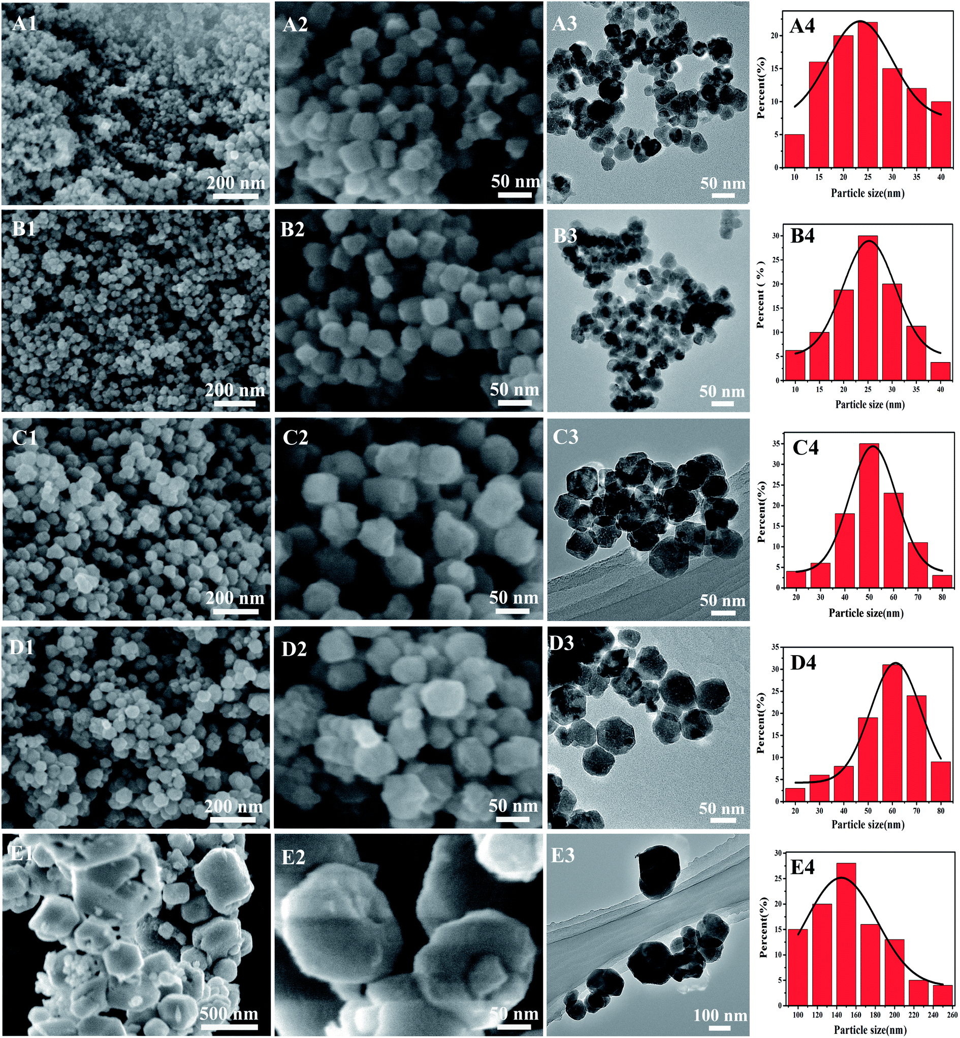 | ||
| Fig. 1 Low (columns 1) and high (columns 2) magnification SEM images, TEM images (columns 3) and size distributions (columns 4) of different shaped Cu2O nanocrystals. A–E corresponding to sample S1–S5 obtained at 110 °C, 120 °C, 130 °C, 140 °C and by DMF refluxed, respectively. | ||
Fig. 1(A1)–(A3) and S1 (ESI†) present the SEM and TEM images of S1 with an average particle size of 25 nm, suggesting that monodispersed particles are not many while aggregation is very obvious. There are many “aggregation units” with sizes of 40–65 nm as shown in Fig. S1 (ESI†). And each “aggregation unit” looks like “single particle” under low magnification (Fig. 1(A3)). It is well known that the smaller particle size is, the more instability is. Fig. 1(A4) shows that the content of particles lower than 20 nm is 41%. Therefore, it is considered that maybe so many ultrafine particles caused aggregation. Further aggregation probably leaded to forming bigger single particle. That is why there are also many particles (21% of the total) bigger than 35 nm (Fig. 1(A4)).
Among the five samples, S2 with an average particle size of 25 nm exhibits uniform size distribution and good dispersal according to Fig. 1(B1)–(B3) and S2 (ESI†). Compared with S1, the particles with sizes smaller than 20 nm decreased as shown in Fig. 1(B4), which maybe results in better dispersal. With the temperature climbing to 130 °C, the average size of S3 increases to 50 nm (relevant information shown in Fig. 1(C1)–(C4)). Moreover, Fig. 1(D1)–(D4) displays some particles of S4 become bigger continuously with an average particle size of 58 nm when the temperature goes up to 140 °C. Moreover, it is analyzed that polyhedron Cu2O has been formed because Quasi-spherical structure is destroyed by the gas bubbles produced during DMF being refluxed. In summary, the particle size becomes bigger as the temperature increases. It is because the reaction speed is accelerated at higher temperature and the disperse ability of PVP is probably weakened.
High-resolution TEM (HRTEM) as shown in Fig. 2 was used to investigate the inner ultrafine structure of S1 and S2, in order to study the influence of morphology on the photocatalytic activity that will be discussed latter. HRTEM image (Fig. 2(a)) shows obviously that the “aggregation unit” is made up of a few 10–20 nm particles, which causes the specific surface area of S1 to decrease greatly. Moreover, Fig. 2(b) suggests that S1 belongs to common Cu2O nanocrystal (“integral particle”) without further fine structure. However, Fig. 2(c) exhibits that S2 has a special nanostructure and belongs to hierarchical nanoclusters (NCs). And the NCs are made up of ultrafine grains with the sizes of 2–7 nm. Due to high surface energy and intrinsic cubic crystal structure, the smaller grains have a high tendency to regrow together, forming bigger NCs. The inserts of Fig. 2(b) and (c) correspond to the white marked regions, which reveal the well-defined S1 and S2. The lattice fringes of the common nanocrystal and NCs have interplanar spacing of 0.247 nm and 0.240 nm, respectively, which is in agreement with the cubic Cu2O (111) planes.15,28 Therefore, it is considered that “aggregation units” and “common structure” will result in the falling of photocatalytic activity of S1 and the former is thought to be the main factor. On the other hand, photocatalytic ability of S2 should be better.
 | ||
| Fig. 2 HRTEM images of Cu2O nanocrystals (S1) obtained at 110 °C (a) and (b) and Cu2O NCs (S2) got at 120 °C (c). The inserts show the marked regions. | ||
Fig. 3 and S3 (ESI†) show the typical (XRD) patterns of the different shaped Cu2O nanocrystals. All the diffraction peaks of cuprous oxide can be indexed to the (110), (111), (200), (220) and (311) facets of a cubic phased Cu2O (JCPDS no. 05-0667), both in peak position and relative intensity. As can be seen, each Cu2O sample has good crystallinity, which is consistent with the HRTEM analysis as shown in Fig. 2(b) and (c). Among samples of S1–S4, there are no obvious changes in the width of XRD diffraction peaks. However, compared with S5 having relative bigger particle size, the peaks of S1–S4 are broadened. It is because Cu2O nanocrystals with smaller size has wider peak, which was also reported by Y. Sui and his coworkers.38 In addition, no other impurities are found in all of the samples, which is also consistent with the FT-IR spectra as will be discussed according to Fig. 4.
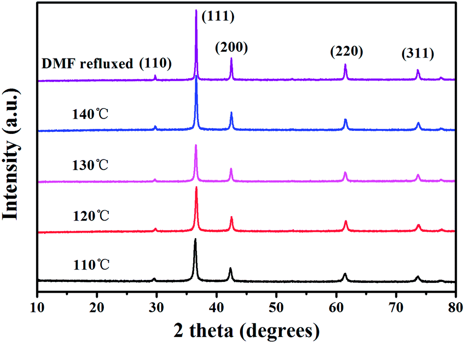 | ||
| Fig. 3 XRD patterns of different shaped Cu2O nanocrystals. | ||
 | ||
| Fig. 4 FT-IR spectra of various shaped Cu2O nanocrystals. | ||
The FTIR spectra were used to examine the purity of different shaped Cu2O nanocrystals as shown in Fig. 4 and S4 (ESI†). There are four peaks in the FTIR spectrum of each sample. The Cu–O vibration was detected at 632 cm−1 and the two peaks at 3447 cm−1 and 1629 cm−1 corresponding to the stretching and bending vibrations of the O–H groups from the unavoidable adsorbed water, while the peak at 1400 cm−1 was attributed to the absorption of carbon dioxide in the air.28,39 Therefore, it can be concluded that no other impurities appeared in each sample, which is in accordance with the XRD analysis.
3.2 Photocatalytic activity
The relationships between the irradiation time and the absorbance at 464 nm of the MO aqueous solution were recorded using various shaped Cu2O nanocrystals as shown in Fig. 5 and S5 (ESI) and Table S1 (ESI).† As can be seen, no changes are observed in the two kinds of concentrations of MO under visible light irradiation in the absence of catalysts (magenta line shown in Fig. 5(a) and (b)). Overall, the photocatalytic activities of different shaped Cu2O nanocrystals weaken as their sizes increase. The order of decomposition rate of five samples is as follows: S2 (120 °C) > S1 (110 °C) > S3 (130 °C) > S4 (140 °C) > S5 (DMF refluxed). And the photocatalytic activities of quasi-spherical Cu2O nanocrystals (black, red, green, blue line) are much better than that of polyhedral Cu2O (cyan line) as shown in Fig. 5(a) and (b). The Cu2O NCs (S2), the best catalyst, could completely degradate the MO solution with the initial concentrations of 10 mg L−1 and 40 mg L−1 in 12 and 65 minutes. | ||
| Fig. 5 Photocatalytic activities and kinetic plots of various shaped Cu2O nanocrystals under visible light irradiation by using different initial concentrations of MO solution ((a) and (c) 10 mg L−1, (b) and (d) 40 mg L−1). The (c) and (d) kinetic plots are based on the data in (a) and (b). | ||
The pseudo-first order reaction was observed for different shaped Cu2O nanocrystals as shown in Fig. 5(c) and (d). The order of the pseudo-first order rate constants (k) is also follows: S2 > S1 > S3 > S4 > S5 (shown in Table S2 (ESI†)). The highest k of S2 calculated are 0.2033 (10 mg L−1) and 0.0053 (40 mg L−1), respectively. The corresponding k values of S5, 0.0533 and 0.0017, are the lowest. The high k value is well known to reflect high photocatalytic activity.15,40 Here, photocatalytic activities of Cu2O crystals towards MO degradation were summarized and listed in Table S3 (ESI†) on the basis of previous literatures. It can be seen clearly that the dosage of S2 is reduced greatly and also does the degradation time compared with other reported Cu2O crystals.
3.3 Analysis of photocatalytic mechanism
It is considered that there are four main factors which lead to S2 with remarkable photocatalytic activity. Firstly, S2 has ultrafine particle, high size uniformity and good dispersal as shown in Fig. 1(B1)–(B4). However, photocatalytic activity of S1 weakens obviously due to serious aggregation of particles and that of S3–S5 also reduces because of bigger particles.Secondly, S2 has ultrafine structure as shown in HRTEM images, which causes it to have strong MO adsorption ability and remarkable photocatalytic activity (Fig. 5(a) and (b)). The mechanism of MO photodegradation with Cu2O as catalyst is schematically illustrated in Fig. 6. And the final degradation products are CO2, H2O and organic compounds.9,41 Previous researches indicate that MO adsorption on Cu2O surface is the pre-procedure in photocatalysis reaction.13,14,23,30–35 It is due to small size effect that both specific surface area and atoms at the surface of Cu2O NCs increase sharply. As a result of partial coordination, the surface atoms are not stable and will combine other encountered atoms quickly for stabilization, which make the photocatalytic active sites and adsorption function increase greatly. On the other hand, oxygen vacancies in Cu2O undoubtedly can act as potential wells to trap either one or two electrons, helping electron–hole pair separation and hence increasing the photocatalytic activity.13 Moreover, it is worthy to point out that photocatalytic activity of hierarchical NCs (S2) is much better than that of “integral particle” with the similar size, which can be proved from the degradation results of Cu2O nanocrystals (S1), TiO2–Cu2O with size of 20–40 nm (ref. 34) and Ag–Cu2O of 60 nm (ref. 35) listed in Table S3 (ESI†). For comparison, the MO adsorption ability and specific surface area of polyhedral Cu2O nanocrystals of 155 nm decrease enormously and so does the photocatalytic activity.
 | ||
| Fig. 6 Schematic diagram of photodegradation mechanism with Cu2O and MO as catalyst and pollutant, respectively. | ||
Thirdly, high separation of the photogenerated carriers (electron–hole pairs) creates excellent photocatalytic activity of S2. It is reported that size of semiconductor nanocrystal is usually smaller than the thickness of spatial electron layer,41 which will make the carriers diffuse Cu2O NCs surface quickly. Then the holes of valence band (h+, VB) will be trapped with H2O and electrons of conduction band (e−, CB) will react with O2 easily. Moreover, diffusion time of the carriers can be expressed with a formula t = d2/k2D (where d is the particle size, k is a constant, and D is the diffusion coefficient of the carriers).42,43 On the basis of the equation, it can be concluded that the smaller particle size is, the shorter time of carriers diffusing from inner to outer will be. As a result, the electron–hole pairs are easier to separate and meanwhile they recombination become harder. Thus the photocatalytic activity is enhanced. As listed in Table S3 (ESI†), the vast difference of degradation rate between S2 and the porous sphere Cu2O of ∼300 nm (ref. 14) attribute to rapid transformation and high separation of carriers also mentioned in other articles.15
Fourthly, quantum size effect is thought to be one of the factors improving photocatalytic activity of S2. Researchers generally think that particle size of semiconductor smaller than the critical value (∼10 nm) will cause obvious quantum size effect shown in Fig. 7, such as CB and VB splitting into discrete energy levels, band gap broadening, VB potential increasing and CB potential decreasing.41 That is, the oxidation ability of h+ and reduction activity of e− will be increased subsequently. Therefore, 6.3% of the Cu2O NCs with size around 10 nm (shown in Fig. 1(B4)) is thought to be leading to the increase of the MO degradation efficiency because of quantum size effect.
 | ||
| Fig. 7 Schematic diagram of the quantum size effect from Cu2O NCs. | ||
4. Conclusions
In summary, a facile strategy to synthesize various shaped Cu2O nanocrystals in DMF medium via the reduction of Cu2+ with NaBH4 and PVP as the dispersing agent are presented. Different shaped Cu2O nanocrystals with average particle sizes ranging from 25 to 155 nm have been obtained by simply changing reaction temperature and duration. It is found that quasi-spherical Cu2O nanocrystals with sizes from 25 to 58 nm have much better photocatalytic activities in the degradation of MO under visible light irritation than that of polyhedral Cu2O nanocrystals of 155 nm. Furthermore, the Cu2O NCs of 25 nm exhibit remarkable photocatalytic ability due to good dispersal, strong MO adsorption and high separation of photo-generated carriers. The results indicate that it is one of important ways to enhance photocatalytic activities of Cu2O and other photocatalyst by decreasing their particle size as possible as we can.Acknowledgements
Support from the National Natural Science Foundation of China (21176246 and 11204371) and the Priority Academic Program Development of Jiangsu Higher Education Institutions are gratefully acknowledged.References
- C. M. McShane and K. S. Choi, J. Am. Chem. Soc., 2009, 131, 2561 CrossRef CAS PubMed.
- L. Wu, L. K. Tsui, N. Swami and G. Zangari, J. Phys. Chem. C, 2010, 114, 11551 CAS.
- M. Hara, T. Kondo, K. Mutsuko, I. Sigeru, S. Kiyoaki, T. Akira, J. Kondo and D. Kazunari, Chem. Commun., 1998, 357 RSC.
- R. Prucek, L. Kvitek, A. Panacek, L. Vancurova, J. Soukupova, D. Jancik and R. Zboril, J. Mater. Chem., 2009, 19, 8463 RSC.
- J. Zhang, J. Liu, Q. Peng, X. Wang and Y. Li, Chem. Mater., 2006, 18, 867 CrossRef CAS.
- D. Fishman, C. Faugeras, M. Potemski, A. Revcolevschi and P. H. Van Loosdrecht, Phys. Rev. B: Condens. Matter Mater. Phys., 2009, 80, 045208 CrossRef.
- C. Zhang, J. Tu, X. Huang, Y. Yuan, X. Chen and F. Mao, J. Alloys Compd., 2007, 441, 52 CrossRef CAS PubMed.
- P. de Jongh and J. Kelly, Chem. Commun., 1999, 1069 RSC.
- P. Sharma and S. K. Sharma, Water Resour. Manage. Ser., 2012, 26, 4525 CrossRef PubMed.
- W. C. Huang, L. M. Lyu, Y. C. Yang and M. H. Huang, J. Am. Chem. Soc., 2012, 134, 1261 CrossRef CAS PubMed.
- H. Xu, W. Wang and W. Zhu, J. Phys. Chem. B, 2006, 110, 13829 CrossRef CAS PubMed.
- J. Y. Ho and M. H. Huang, J. Phys. Chem. C, 2009, 113, 14159 CAS.
- Y. Zhang, B. Deng, T. Zhang, D. Gao and A. W. Xu, J. Phys. Chem. C, 2010, 114, 5073 CAS.
- L. Feng, C. Zhang, G. Gao and D. Cui, Nanoscale Res. Lett., 2012, 7, 1 CrossRef PubMed.
- A. Abulizi, G. H. Yang and J. J. Zhu, Ultrason. Sonochem., 2014, 21, 129 CrossRef CAS PubMed.
- B. Balamurugan and B. Mehta, Thin Solid Films, 2001, 396, 90 CrossRef CAS.
- Z. C. Orel, A. Anzlovar, G. Drazic and M. Zigon, Cryst. Growth Des., 2007, 7, 453 CAS.
- M. Wei and J. Huo, Mater. Chem. Phys., 2010, 121, 291 CrossRef CAS PubMed.
- J. H. Zhong, G. R. Li, Z. L. Wang, Y. N. Ou and Y. X. Tong, Inorg. Chem., 2010, 50, 757 CrossRef PubMed.
- L. Gou and C. J. Murphy, Nano Lett., 2003, 3, 231 CrossRef CAS.
- A. Radi, D. Pradhan, Y. Sohn and K. Leung, ACS Nano, 2010, 4, 1553 CrossRef CAS PubMed.
- C. H. Kuo and M. H. Huang, J. Am. Chem. Soc., 2008, 130, 12815 CrossRef CAS PubMed.
- Y. Yu, L. Zhang, J. Wang, Z. Yang, M. Long, N. Hu and Y. Zhang, Nanoscale Res. Lett., 2012, 7, 1 CrossRef PubMed.
- H. Wang, S. He, S. Yu, T. Shi and S. Jiang, Powder Technol., 2009, 193, 182 CrossRef CAS PubMed.
- W. Chen, L. Li, Q. Peng and Y. Li, Nano Res., 2012, 5, 320 CrossRef CAS PubMed.
- S. Dehghanpour, A. Mahmoudi, M. M. Ghazi, N. Bazvand, S. Shadpour and A. Nemati, Powder Technol., 2013, 246, 148 CrossRef CAS PubMed.
- L. Huang, F. Peng, H. Yu and H. Wang, Mater. Res. Bull., 2008, 43, 3047 CrossRef CAS PubMed.
- D. L. Zhou, J. J. Feng, L. Y. Cai, Q. X. Fang, J. R. Chen and A. J. Wang, Electrochim. Acta, 2014, 115, 103 CrossRef CAS PubMed.
- C. Kuo, C. Chen and M. H. Huang, Adv. Funct. Mater., 2007, 17, 3773 CrossRef CAS PubMed.
- J. Dai, X. Fan, H. Liu, J. Wang, H. Liu and F. Zhang, J. Nanosci. Nanotechnol., 2012, 12, 6412 CrossRef CAS PubMed.
- Q. Hua, F. Shi, K. Chen, S. Chang, Y. Ma, Z. Jiang, G. Pan and W. Huang, Nano Res., 2011, 4, 948 CrossRef CAS.
- L. Pan, L. Li and Y. Chen, Micro Nano Lett., 2011, 6, 1019 CAS.
- Z. P. Li, Y. Q. Wen, J. P. Shang, M. X. Wu, L. F. Wang and Y. Guo, Chin. Chem. Lett., 2013, 25, 287 CrossRef PubMed.
- L. Huang, S. Zhang, F. Peng, H. Wang, H. Yu, J. Yang, S. Zhang and H. Zhao, Scr. Mater., 2010, 63, 159 CrossRef CAS PubMed.
- X. Lin, R. Zhou, J. Zhang and S. Fei, Appl. Surf. Sci., 2009, 256, 889 CrossRef CAS PubMed.
- K. Nishimura, J. L. C. Huaman, M. Hiroshi, T. Akiyama, T. Oku and B. Jeyadevan, Mater. Res. Express, 2014, 1, 015032 CrossRef.
- M. Yin, C. K. Wu, Y. Lou, C. Burda, J. T. Koberstein, Y. Zhu and S. O'Brien, J. Am. Chem. Soc., 2005, 127, 9506 CrossRef CAS PubMed.
- Y. Sui, Y. Zeng, L. Fu, W. Zheng, D. Li, B. Liu and B. Zou, RSC Adv., 2013, 3, 18651 RSC.
- Y. Zhang, D. Wang, X. Zhang and F. Qu, J. Nanomater., 2013, 2013, 1 Search PubMed.
- H. Hou, L. Wang, F. Gao, G. Wei, J. Zheng, B. Tang and W. Yang, RSC Adv., 2014, 4, 19939 RSC.
- L. D. Zhang and J. M. Mou, Nano-material and nanostructure, Science Press, Beijin, 2001, p. 89 Search PubMed.
- L. Liang, Y. Sun, F. Lei, S. Gao and Y. Xie, J. Mater. Chem. A, 2014, 2, 10647 CAS.
- L. Yan, W. Bin and W. Qian, Chin. Phys. B, 2012, 21, 098102 CrossRef.
Footnote |
| † Electronic supplementary information (ESI) available. See DOI: 10.1039/c4ra06119e |
| This journal is © The Royal Society of Chemistry 2014 |