
 Open Access Article
 This Open Access Article is licensed under a
 Creative Commons Attribution 3.0 Unported Licence
Efficiency droop in zincblende InGaN/GaN quantum wells†
D. Dyer a,
S. A. Churcha,
R. Ahumada-Lazoab,
M. J. Kappersc,
M. P. Halsalld,
P. Parkinsona,
D. J. Wallisce,
R. A. Oliverc and
D. J. Binks*a
a,
S. A. Churcha,
R. Ahumada-Lazoab,
M. J. Kappersc,
M. P. Halsalld,
P. Parkinsona,
D. J. Wallisce,
R. A. Oliverc and
D. J. Binks*a
aDepartment of Physics and Astronomy & Photon Science Institute, University of Manchester, Manchester, M13 9PL, UK. E-mail: david.binks@manchester.ac.uk
bTecnologico de Monterrey, School of Engineering and Sciences, Ave. Eugenio Garza Sada 2501, Monterrey, N.L. 64849, Mexico
cDepartment of Materials Science and Metallurgy, University of Cambridge, Cambridge, CB3 0FS, UK
dDepartment of Electrical and Electronic Engineering & Photon Science Institute, University of Manchester, Manchester, M13 9PL, UK
eCentre for High frequency Engineering, Cardiff University, Cardiff, CF24 3AA, UK
First published on 3rd July 2024
Abstract
The decrease in emission efficiency with increasing drive current density, known as ‘droop’, of c-plane wurtzite InGaN/GaN quantum wells presently limits the use of light-emitting diodes based on them for high brightness lighting applications. InGaN/GaN quantum wells grown in the alternative zincblende phase are free of the strong polarisation fields that exacerbate droop and so were investigated by excitation-dependent photoluminescence and photoreflectance studies. Polarisation-resolved measurements revealed that for all excitation densities studied the emission from such samples largely originates from similar microstructures or combinations of microstructures that form within the quantum well layers. Emission efficiency varies significantly with excitation at 10 K showing that non-radiative recombination processes are important even at low temperature. The onset of efficiency droop, as determined by photomodulated reflection measurements, occurred at a carrier density of around 1.2 × 1020 cm−3 – an order of magnitude greater than the value reported for a reference wurtzite quantum well sample using the same method. The high carrier density droop onset combined with the much shorter carrier lifetime within zincblende InGaN/GaN quantum wells indicate they have the potential to effectively delay efficiency droop when used in GaN based light-emitting diodes. However, the material quality of the quantum well layers need to be improved by preventing the formation of microstructures within these layers, and the importance of the role played by non-radiative centres in the QW layer needs to be elucidated, to fully realise the material's potential.
I. Introduction
Currently, the leading light-emitting diode (LED) technology for lighting applications is based on c-plane wurtzite (wz) InGaN/GaN quantum wells (QWs), for which power conversion efficiencies exceeding 80% can be achieved at blue wavelengths.1 However, a process known as efficiency droop severely limits the brightness that can be achieved for wz-InGaN/GaN LEDs.2,3 This can cause the efficiency to drop to 44% and 26% (for an injection current density of 40 A cm−2) in commercial-grade blue- and green- emitting InGaN LEDs, respectively.4 Several possible causes for efficiency droop have been proposed including Auger–Meitner recombination,5,6 the quantum-confined Stark effect,7 carrier leakage and poor hole injection,2,8,9 and carrier delocalisation leading to increased Shockley–Read–Hall (SRH) recombination.10–13 However, recent work by Li et al. has reported that defect related recombination such as SRH and trap-assisted Auger–Meitner recombination has little influence on the droop process within current state of the art green LEDs.14Growing wz-QWs along other crystallographic directions may reduce efficiency droop because these alternative structures benefit from a significantly reduced or eliminated field across the QW, which in c-plane structures can be on the order of MV m−1 and originates from the strong spontaneous and piezoelectric polarisation produced at the InGaN/GaN interface. The reduction or absence of these internal electric fields in such semi-polar or non-polar structures brings a number of potential benefits. These include improved confinement, which can reduce losses associated with carrier spillage,15,16 better hole distribution among QWs in multiple QW (MQW) structures,16 reduced Auger–Meitner recombination,17 and lower operating carrier densities due to shorter recombination lifetimes.18–20 A comparison of c-plane and non-polar m-plane wz-InGaN/GaN structures showed that the droop onset occurred at almost identical carrier densities, indicating that the benefit for m-plane devices is principally due to their much shorter recombination lifetimes.18
In recent years, InGaN/GaN QWs grown in the zincblende (zb) phase have arisen as a promising alternative to the wz structure. Zb-QWs are free of the internal electric fields found in c-plane wz-QWs when grown along the (001) direction21 and exhibit sub-nanosecond radiative recombination lifetimes,22 two orders of magnitude lower than those typically found for c-plane QWs.23 However, the microstructure of zb-QWs can be significantly different from that of their polar and non-polar wz analogues. Considerable indium segregation has been observed adjacent to the stacking faults that penetrate the QW layers,24 leading to the formation of quantum-wires (QWires) within the QW.22,24,25 Stacking faults with the (−111) and (111) orientation were found to dominate,26 which would be expected to produce QWires and thus polarised emission along both the [110] and [1−10] directions. The droop process in zb-QW samples with high stacking fault densities is therefore expected to be more complex than the process in the wz phase with possible contributions to the emission from two populations of perpendicularly orientated QWires as well as other parts of the QWs. Thus, to enable a full assessment of their merits, this paper investigates efficiency droop in zb-QW samples and compares it to that found in wurtzite structures.
II. Experimental methods
A. Sample details
The samples used in this study were grown by metalorganic chemical vapor deposition (MOCVD) on 3C-SiC/Si (001) substrates using an Aixtron 1 × 6 in. CCS shower head reactor, and are shown in Fig. 1. Each sample consisted of a 30 nm thick nucleation layer, a 200 nm thick zb-GaN buffer layer, a 500 nm Si:GaN layer, and a 40 nm unintentionally doped InGaN underlayer (UL) with various QW structures grown on top. Four different samples were produced: a single QW (SQW) with a nominal width of 2.5 nm and three MQW structures consisting of 5 QWs with nominal widths varying from 2.5, 5 to 7.5 nm; the cap layer and the barriers between QWs consisted of 8 nm thick GaN layers. Further details of the growth method used can be found in a previous publication.27 Previous samples, grown under very similar conditions, show that the InGaN QW layer retains the zincblende structure of the underlying GaN layer. This has been assessed using both high resolution scanning transmission electron microscopy (STEM)24 and scanning electron diffraction (SED).28 Although the SED experiments did reveal very occasional regions of hexagonal material a few tens of nanometres in size in the QW, cathodoluminescence (CL) imaging confirmed that these regions have little influence on the overall emission spectrum.28 As detailed previously,25 the presence of stacking faults in these samples leads to the QW layers having a non-planar geometry, thus an accurate value for the indium content within the QW layers cannot be obtained from X-ray diffraction measurements. Instead, the indium composition was estimated from the position of the photoluminescence (PL) peak at low excitation. This method resulted in values of (9 ± 0.5)% and (10 ± 0.5)% for the SQW and MQWs, respectively, and of (22.5 ± 0.5)% and (20.0 ± 0.5)% in the QWires that form within the SQW and MQWs.25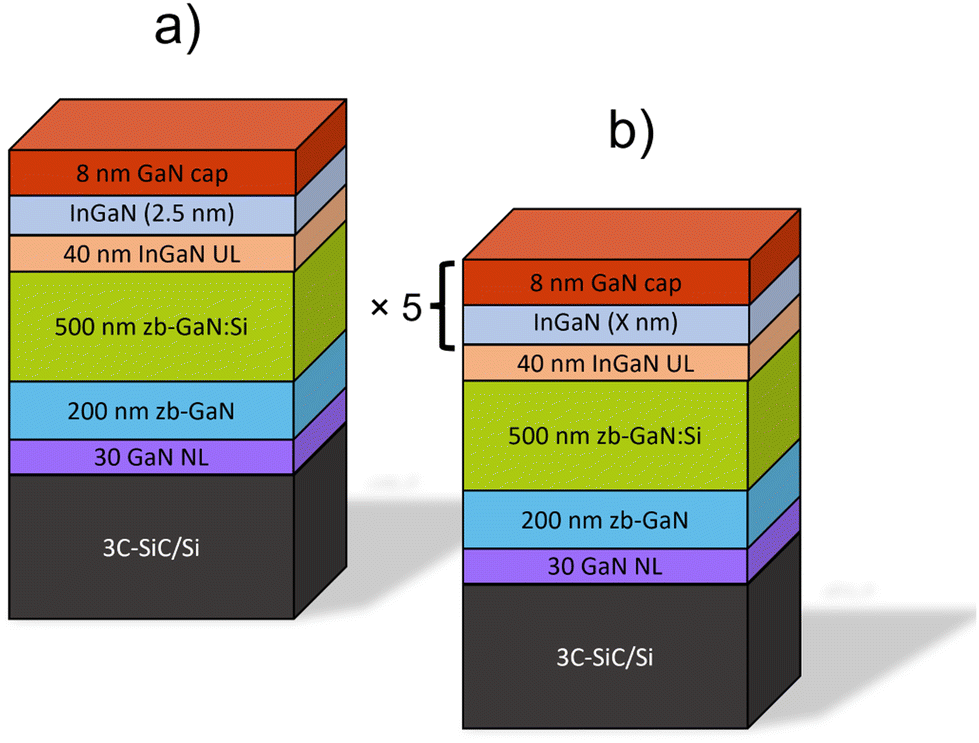 | ||
| Fig. 1 Diagram of (a) zb-SQW and (b) MQW samples used in this study. | ||
B. Photoluminescence
Low temperature PL measurements were obtained by mounting the samples onto the cold finger of an evacuated closed cycle He cryostat and excited above the bandgap of zb-GaN (3.3 eV at 10 K (ref. 29)) using the 325 nm (3.8 eV) line of a continuous wave (CW) 10 mW HeCd laser – which was focused onto the sample with a 7.5 cm focal length lens to achieve a 37 μm spot size. The PL emission was collected and focused into the entrance slit of a spectrometer with a spectral resolution of 4.8 nm, before being detected by a photomultiplier tube (PMT). A mechanical chopper modulated the HeCd laser – the reference signal from which was passed onto a Stanford Instruments lock-in amplifier along with the PMT signal to perform phase sensitive detection to increase the signal-to-noise ratio. Neutral density (ND) filters were employed to change the power density incident at the samples. Polarisation resolved droop measurements were obtained by employing a normal angle of incidence for the excitation beam and a Glan–Thompson polariser to resolve the PL spectra along the crystallographic directions of the samples.C. Combined photoluminescence and photomodulated reflection
Combined PL and photoreflection (PR) measurements were conducted at room temperature, in a similar manner to ref. 30, to measure the carrier density corresponding to the onset of droop in the zb-QW samples. Firstly, the variation of emission efficiency with incident power density was determined using a CW 405 nm laser to resonantly excite the QWs and so avoid inhomogeneous carrier distribution effects (see section IIIA2), with ND filters employed to alter the excitation power density. The light was focused onto the sample using a microscope objective and the sample emission was collected by the same objective and sent to a fibre coupled spectrometer. Secondly, the relationship between the power density incident on the sample and the resulting carrier density generated was obtained from PR measurements. The same 405 nm CW laser was employed as the pump laser which was modulated internally by the laser power supply to periodically excite the zb-MQW sample. A 660 nm probe laser was also focused onto the pump beam using the microscope objective. The pump beam creates a photo-induced change in the reflectivity of the sample, causing a periodic modulation of the reflected probe beam at the same frequency. The reflected signal from the 660 nm laser is detected by a silicon photodiode, which is then passed onto a lockin-amplifier along with the reference signal from the pump laser power supply. The carrier density is calculated from this PR data by the method detailed in the ESI.† Further information on this technique can be found in ref. 30.III. Results
A. Physics of efficiency droop in zb-QWs
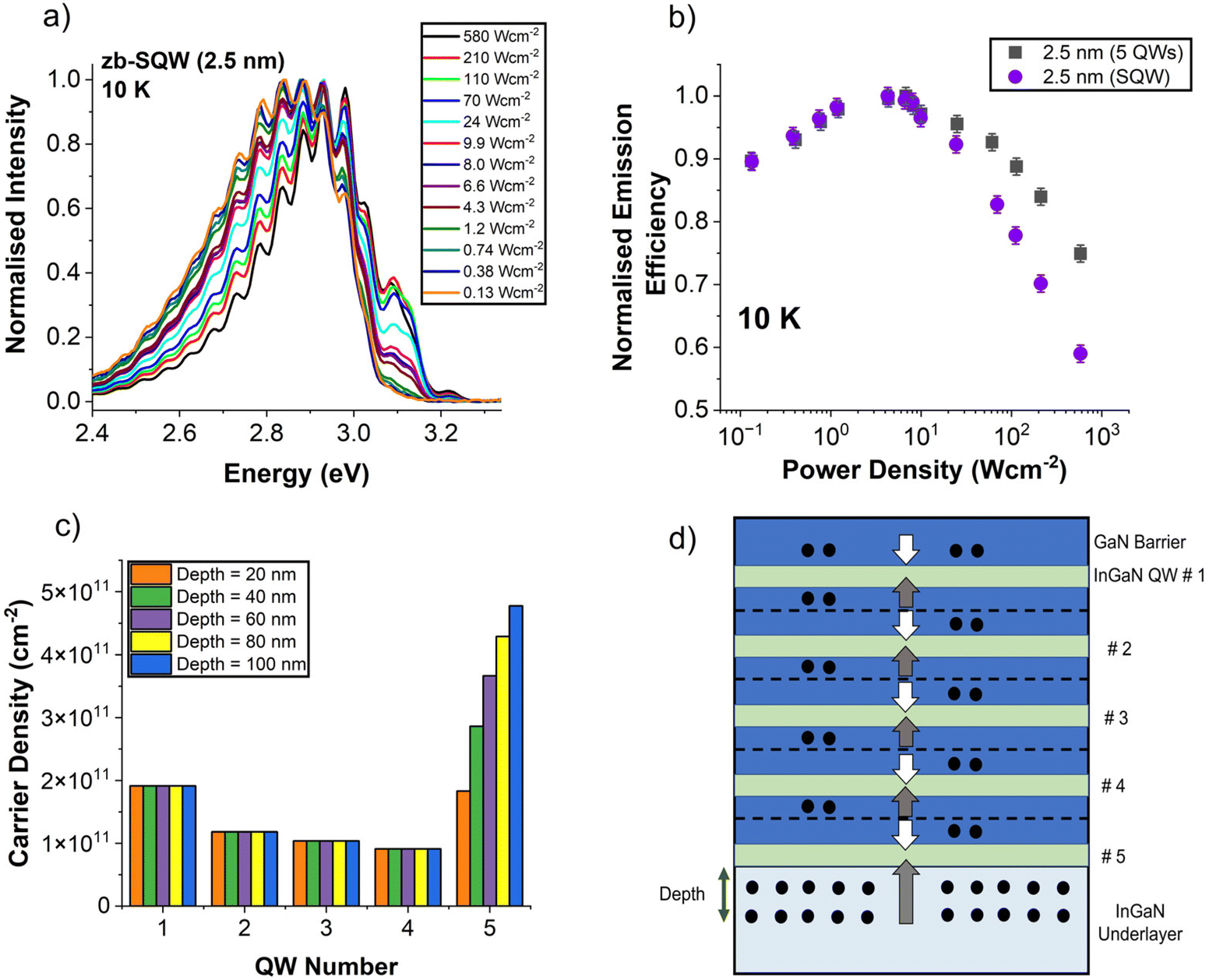 | ||
| Fig. 2 (a) 10 K power density dependent PL spectra for a zb-SQW sample excited at 325 nm, (b) comparison of the 10 K droop curves for a SQW and MQW samples with well width = 2.5 nm. (c) Calculated carrier density in each of the QWs within the MQW stack as a function of the depth into the underlayer. (d) Schematic diagram illustrating the regions from which each QW captures carriers, as assumed in the calculation of the carrier density in each QW. The arrows show the directions carriers move to reach the nearest QW. | ||
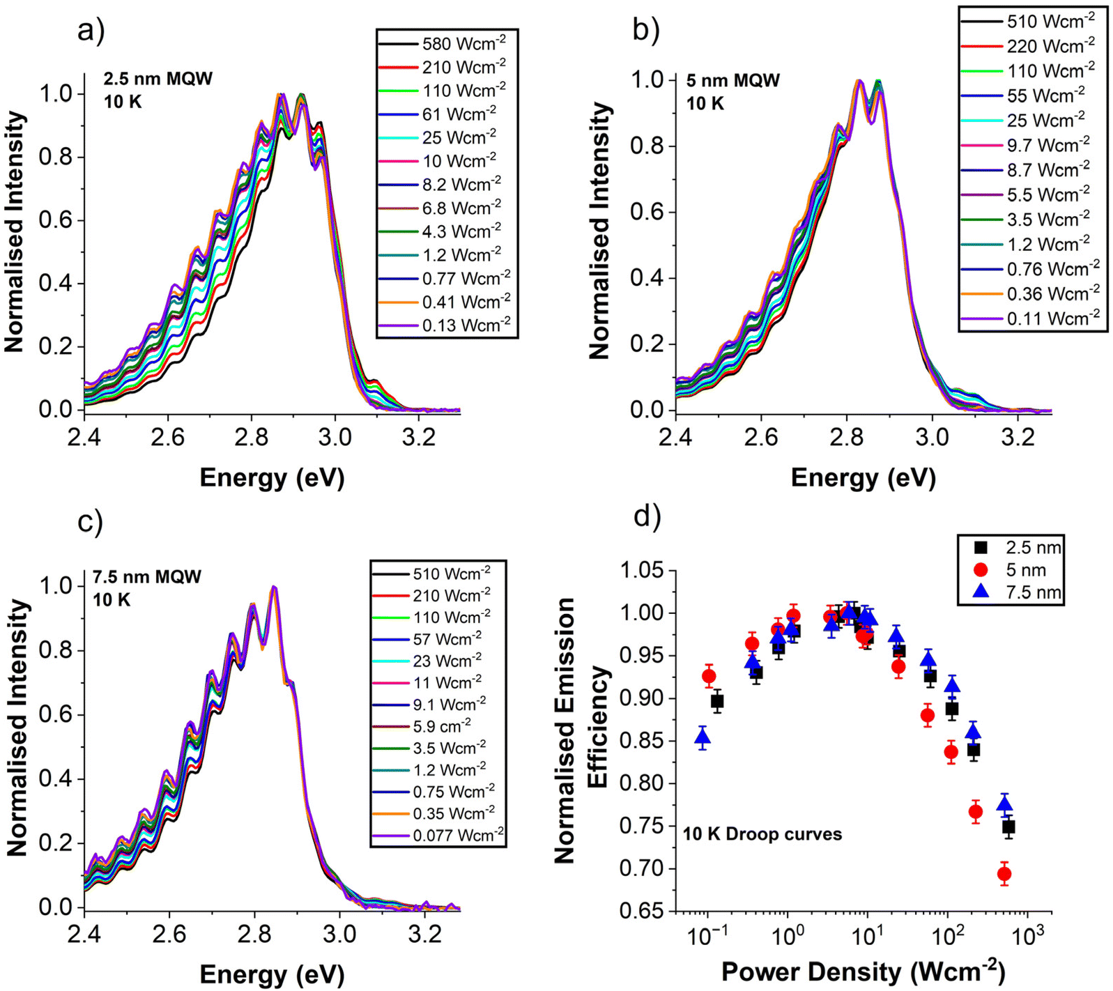 | ||
| Fig. 3 Power density dependent emission spectrum for MQWs with well widths of (a) 2.5 nm, (b) 5 nm, and (c) 7.5 nm. (d) 10 K droop response comparison of the MQW samples. | ||
A comparison of the normalised PL and droop curves for the MQW samples with different well widths is shown in Fig. 3. The PL emission from the samples again show a reduction in FWHM as the power density increases – resulting from a decreased intensity on the low energy side of the PL spectra, although this affect appears to reduce as the well width increases. The 3.1 eV peak is also visible in the 2.5 nm sample but the relative intensity of this feature decreases as well width increases, and is no longer visible in the 7.5 nm sample. The efficiency curves for the three samples are broadly similar, with no systematic changes in droop onset or rate of subsequent efficiency decrease with well width seen. The Auger–Meitner recombination process would be expected to reduce as QW width increases due to the reduced carrier density present within the QWs. However, as no significant change in the droop curve with QW width is observed in these zb-QWs, this indicates Auger–Meitner recombination is not the dominant process limiting efficiency at power densities exceeding 10 W cm−2. Rather, the emergence of the peak at 3.1 eV at high excitation suggests increased carrier recombination in the GaN is occurring due to e.g. carrier overflow.
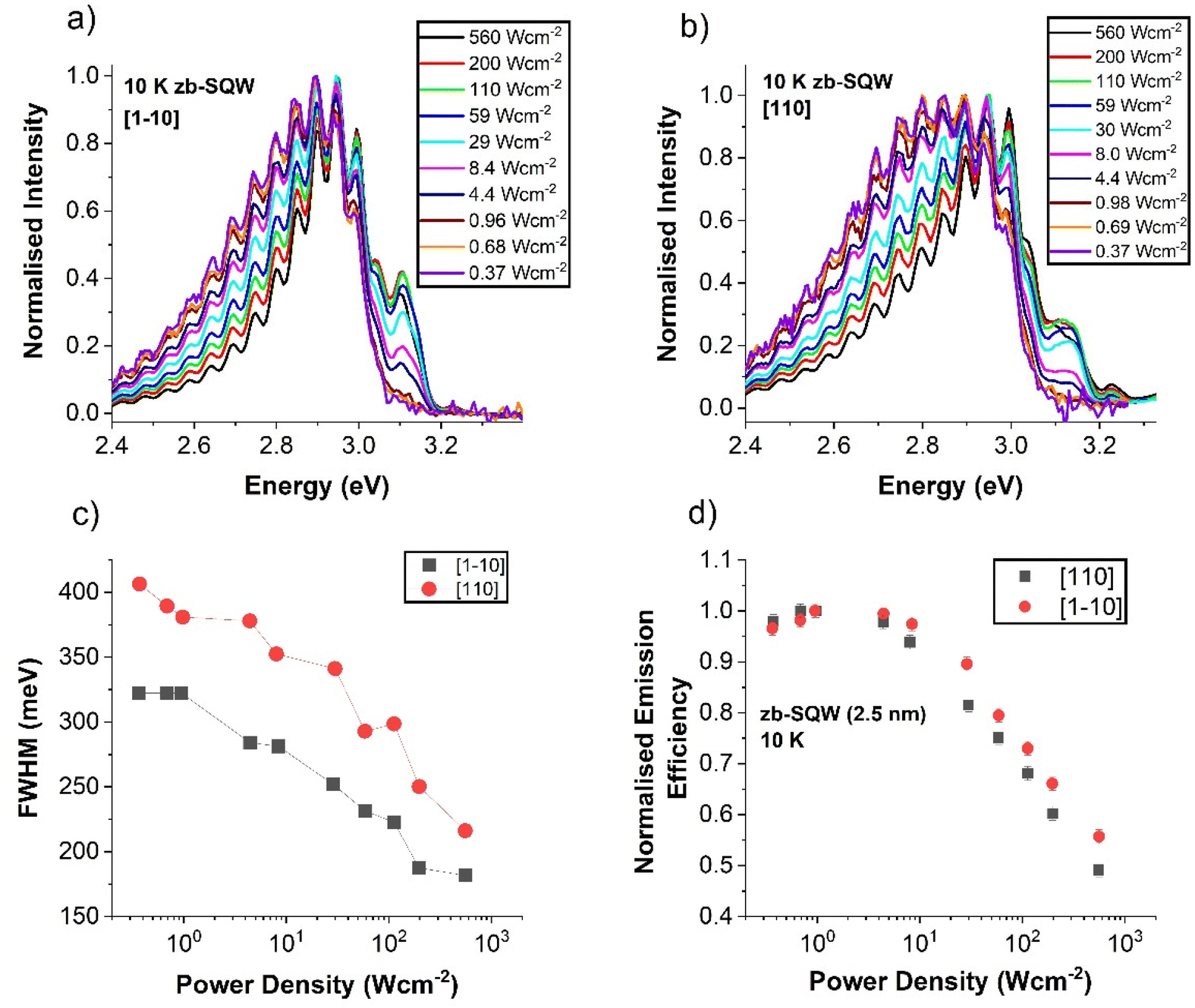 | ||
| Fig. 4 Power density dependent PL along (a) the [1−10] direction and (b) [110] direction. (c) FWHM of the PL along these two directions as a function of power density and (d) efficiency droop curves along these two directions. | ||
The similar PL emission response to increasing power density observed in this work for both polarisation directions indicates that rather than the emission originating from a more polarised QWire emission combined with less polarised QW emission as reported previously,22 the emission in these samples originates from the same type of microstructure or combinations of microstructures within the QW layer. Future polarisation-filtered scanning electron microscopy cathodoluminescence (SEM-CL) measurements may be able to help identify the links between polarised light emission and microstructure.
B. Carrier density dependence of droop
The efficiency droop in zb-QW samples has been presented as a function of excitation power density in the previous section. However, the key processes that determine efficiency droop within GaN-based QWs depend upon the carrier density, n, within them.35 Determination of carrier density from excitation rate is not straightforward. The carrier density generated by steady-state excitation depends not only on the excitation rate but also on the carrier lifetime, which varies both across the emission spectrum36 and with excitation rate. Thus, the calculation of carrier density from steady-state excitation requires a detailed characterisation of the carrier lifetime by, for example, differential carrier lifetime measurements.37 Furthermore, calculating the carrier density for above bandgap excitation requires an understanding of the capture efficiency of photogenerated carriers into each of the QWs in a stack and may result in an inhomogeneous carrier distribution. PR measurements can be used to determine steady-state n without characterising the carrier lifetime. (Note that the depth sensitivity of PR measurements is limited by the wavelength of the probe used (660 nm in this case) and so does not distinguish between carriers in the QWs or in the nearby GaN regions.) Thus, to build an overall picture of the dependence of efficiency droop on carrier density in zb-QWs, the carrier density dependence of emission efficiency for the 5 nm zb-MQW sample was investigated by the pump probe PR technique with the 405 nm pump laser directly exciting the QW layers. Full details of the technique, as well as the process to extract carrier density from the experimental data can be found in ref. 30.Fig. 5 compares the emission efficiency (calculated as the spectrally-integrated emission intensity/incident power density) and carrier density determined from the combined PL and PR measurements, both as a function of steady-state excitation power density. This comparison shows that the emission efficiency and carrier density respond to increasing excitation in a similar way: rising at low excitation before reaching a maximum at the same excitation density and then decreasing. The onset of sample heating – shown by the small apparent decrease in the carrier density at high power densities in Fig. 5 – limits the maximum power density that can be used in the PR measurement which is why it does not span the same range as the efficiency curve in Fig. 5. However, before the onset of thermal effects, it can be assumed the carrier densities are accurate. The peak emission efficiency (spectrally integrated intensity/incident power density) occurs at an excitation density corresponding to a carrier density of approximately 1.2 × 1020 cm−3. The same technique (and experimental set-up) has been previously used to measure droop in 2.5 nm thick wz-InGaN/GaN QWs, allowing a direct comparison between the polytypes. For the wz-InGaN/GaN QWs, the onset of droop thus measured occurred at a carrier density of 1 × 1019 cm−3 i.e. an order of magnitude lower than for the zb-QW samples studied here.30
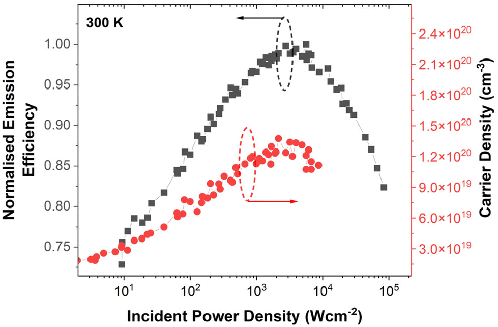 | ||
| Fig. 5 Emission efficiency and carrier density determined by PL and PR measurements, respectively, for the 5 nm zb-MQW sample as a function of resonant steady-state laser excitation power density at 300 K. | ||
IV. Discussion
The results presented in section III B indicate that the peak emission efficiency of zb-QWs occurs at a carrier density about one order of magnitude greater than for wz-QWs. There are a number of factors that could contribute to this difference. The absence of a strong polarisation field in zb-QWs enables significant exciton formation, as evidenced by mono-exponential recombination dynamics,22 which will persist to room temperature since the exciton binding energy in zb-GaN is about 26 meV.38 The consequent co-localisation of electron–hole pairs also tends to increase the radiative recombination rate, consistent with the sub-nanosecond PL lifetimes observed at low temperature that are largely independent of QW width.25It is also possible that a high total rate of non-radiative processes is competing with radiative recombination to a significant degree until greater levels of excitation, resulting in a higher carrier density corresponding to peak efficiency but at the expense of lower efficiencies overall. Thus, an understanding of the non-radiative recombination centres present in the QW layer, their densities, and how they compete with the other recombination processes is crucial to elucidate if the higher droop onset of zb-QWs is beneficial for high brightness LED applications.
It is important to note there is evidence of a significant amount of thermionic emission from these samples, with a steep drop in efficiency reported previously as the temperature is increased from 10 K to room temperature for the SQW sample that is significantly ameliorated for the otherwise similar MQW sample.22,25 This suggests that carriers are escaping the QW at higher temperatures and are more likely to be recaptured in a MQW structure. Thermionic emission from these samples is likely exacerbated by the broad range of energy states in the zb-QWs that extends close to the band edge of the barriers, cap and UL, as demonstrated by the emission spectrum shown in Fig. 2. This suggests that increasing the indium content of the zb-QWs may significantly reduce carrier escape from the QWs by increasing the energy barrier to escape. The distinct microstructure of zb-QWs compared to their wz analogues is also an important consideration. At present, it is unclear how carriers are distributed amongst the structures that form within the zb-QW layers. SEM-CL measurements could contribute to an understanding of the microstructural origins of the QW luminescence, assess the material quality of the QW layer and identify any variations in these parameters as a function of QW width and number.
V. Summary and conclusion
Efficiency droop in zb-QW samples was investigated using photoluminescence and photomodulated reflection measurements. Emission efficiency varies significantly with excitation at 10 K showing that non-radiative recombination processes are important even at low temperature. Increasing the number of QWs resulted in a reduction in the rate of droop while the droop onset remained the same suggesting an inhomogeneity in the distribution of carriers amongst the QWs for above gap excitation. In contrast, increasing the well width from 2.5–7.5 nm had little effect on the dependence of emission efficiency on excitation. The emission from each of these samples is significantly polarised, which is attributed to the microstructure of the QWs; the similar nature of this polarised emission from each of the samples thus indicates that each of the samples studied contains similar microstructures or combinations of microstructures. The onset of efficiency droop in the 5 nm QW sample, as determined by photomodulation reflection measurements, occurred at a carrier density of around 1.2 × 1020 cm−3 an order of magnitude greater than values reported for wz-GaN QWs using the same method. Whilst the higher carrier density corresponding to droop onset combined with the much shorter carrier lifetime within this sample indicate the material has the potential to effectively delay efficiency droop within GaN based LEDs, improved confinement of the carriers will be necessary to reduce thermionic emission and the importance of the role played by non-radiative centres in the QW layer will need to be investigated further to fully realise this benefit.Author contributions
Samples for this study were grown by M. J. Kappers, with experiments conducted by D. Dyer, M. P. Halsall and S. A. Church. Funding sourced by D. J. Wallis, R. A. Oliver and D. J. Binks. Initial manuscript written by D. Dyer, S. A. Church, R. Ahumada-Lazo and D. J. Binks. All authors contributed to the editing of this manuscript.Data availability
The data underlying this study are openly available in the University of Manchester Repository at https://doi.org/10.48420/25288408.Conflicts of interest
DJ Wallis is a director of Kubos Semiconductors Ltd which supplied the SiC/Si substrates for this work and is commercially exploiting patents developed by authors S. A. Church, M. J. Kappers, D. J. Wallis, R. A. Oliver and D. J. Binks.Acknowledgements
The authors would like to acknowledge funding and support from the Engineering and Physics Sciences Research Council (EPSRC) under Grant Codes EP/W034956/1, EP/R010250/1, EP/R01146X/1 and EP/W035871/1. D. Dyer would also like to acknowledge support through the EPSRC Doctoral Training Partnership.References
- Y. Narukawa, M. Ichikawa, D. Sanga, M. Sano and T. Mukai, White light emitting diodes with super-high luminous efficacy, J. Phys. D: Appl. Phys., 2010, 43, 354002 CrossRef.
- J. Cho, E. F. Schubert and J. K. Kim, Efficiency droop in light emitting diodes: Challenges and counter measures, Laser Photonics Rev., 2013, 7, 408–421 CrossRef CAS.
- J. Piprek, Efficiency droop in nitride-based light-emitting diodes, Phys. Status Solidi A, 2010, 207, 2217–2225 CrossRef CAS.
- X. Li, N. Pant, E. DeJong, A. T. Elshafiey, R. Armitage, E. Kioupakis and D. Feezell, Carrier dynamics in blue, cyan, and green InGaN/GaN LEDs measured by small-signal electroluminescence, Appl. Phys. Lett., 2023, 122, 212108 CrossRef CAS.
- N. F. Gardner, G. O. Müller, Y. C. Shen, G. Chen, S. Watanabe, W. Götz and M. R. Krames, Blue-emitting InGaN-GaN double-heterostructure light-emitting diodes reaching maximum quantum efficiency above 200 A/cm2, Appl. Phys. Lett., 2007, 91, 243506 CrossRef.
- J. Iveland, L. Martinelli, J. Peretti, J. S. Speck and C. Weisbuch, Direct measurement of auger electrons emitted from a semiconductor light-emitting diode under electrical injection: Identification of the dominant mechanism for efficiency droop, Phys. Rev. Lett., 2013, 110, 177406 CrossRef PubMed.
- E. Kioupakis, Q. Yan and C. G. Van de Walle, Interplay of polarization fields and Auger recombination in the efficiency droop of nitride light-emitting diodes, Appl. Phys. Lett., 2012, 101, 231107 CrossRef.
- J. Xie, X. Ni, Q. Fan, R. Shimada, Ü. Özgür and H. Morkoç, On the efficiency droop in InGaN multiple quantum well blue light emitting diodes and its reduction with p-doped quantum well barriers, Appl. Phys. Lett., 2008, 93, 121107 CrossRef.
- M. F. Schubert, Q. Dai, J. Xu, J. K. Kim and E. F. Schubert, Electroluminescence induced by photoluminescence excitation in GaInN/GaN light-emitting diodes, Appl. Phys. Lett., 2009, 95, 191105 CrossRef.
- B. Monemar and B. E. Sernelius, Defect related issues in the “current roll-off” in InGaN based light emitting diodes, Appl. Phys. Lett., 2007, 91, 181103 CrossRef.
- J. Hader, J. V. Moloney and S. W. Koch, Density-activated defect recombination as a possible explanation for the efficiency droop in GaN-based diodes, Appl. Phys. Lett., 2010, 96, 221106 CrossRef.
- S. Hammersley, T. J. Badcock, D. Watson-Parris, M. J. Godfrey, P. Dawson, M. J. Kappers and C. J. Humphreys, Study of efficiency droop and carrier localisation in an InGaN/GaN quantum well structure, Phys. Status Solidi C, 2011, 8, 2194–2196 CrossRef CAS.
- D. S. P. Tanner, P. Dawson, M. J. Kappers, R. A. Oliver and S. Schulz, Polar InGaN/GaN quantum wells: Revisiting the impact of carrier localization on the green gap problem, Phys. Rev. Appl., 2020, 13, 044068 CrossRef CAS.
- X. Li, E. DeJong, R. Armitage, A. M. Armstrong and D. Feezell, Influence of trap-assisted and intrinsic Auger-Meitner recombination on efficiency droop in green InGaN/GaN LEDs, Appl. Phys. Lett., 2023, 123, 112109 CrossRef CAS.
- S. C. Ling, T. C. Lu, S. P. Chang, J. R. Chen, H. C. Kuo and S. C. Wang, Low efficiency droop in blue-green m-plane InGaN/GaN light emitting diodes, Appl. Phys. Lett., 2010, 96, 231101 CrossRef.
- X. Li, X. Ni, H. Y. Liu, F. Zhang, S. Liu, J. Lee, V. Avrutin, Ü. Özgür, T. Paskova, G. Mulholland, K. R. Evans and H. Morkoç, On the reduction of efficiency loss in polar c -plane and non-polar m -plane InGaN light emitting diodes, Phys. Status Solidi C, 2011, 8, 1560–1563 CrossRef CAS.
- R. Vaxenburg, A. Rodina, E. Lifshitz and A. L. Efros, The role of polarization fields in Auger-induced efficiency droop in nitride based light-emitting diodes, Appl. Phys. Lett., 2013, 103, 221111 CrossRef.
- M. J. Davies, P. Dawson, S. Hammersley, T. Zhu, M. J. Kappers, C. J. Humphreys and R. A. Oliver, Comparative studies of efficiency droop in polar and non-polar InGaN quantum wells, Appl. Phys. Lett., 2016, 108, 252101 CrossRef.
- S. Marcinkevičius, K. M. Kelchner, L. Y. Kuritzky, S. Nakamura, S. P. Denbaars and J. S. Speck, Photoexcited carrier recombination in wide m-plane InGaN/GaN quantum wells, Appl. Phys. Lett., 2013, 103, 111107 CrossRef.
- G. A. Garrett, H. Shen, M. Wraback, A. Tyagi, M. C. Schmidt, J. S. Speck, S. P. DenBaars and S. Nakamaura, Comparison of time-resolved photoluminescence from InGaN single quantum wells grown on nonpolar and semipolar bulk GaN substrates, Phys. Status Solidi C, 2009, 6, S800–S803 Search PubMed.
- D. R. Elsaesser, M. T. Durniak, A. S. Bross and C. Wetzel, Optimizing GaInN/GaN light-emitting diode structures under piezoelectric polarization, J. Appl. Phys., 2017, 122, 115703 CrossRef.
- S. A. Church, B. Ding, P. W. Mitchell, M. J. Kappers, M. Frentrup, G. Kusch, S. M. Fairclough, D. J. Wallis, R. A. Oliver and D. J. Binks, Stacking fault-associated polarized surface-emitted photoluminescence from zincblende InGaN/GaN quantum wells, Appl. Phys. Lett., 2020, 117, 032103 CrossRef CAS.
- G. Christian, M. Kappers, F. Massabuau, C. Humphreys, R. Oliver and P. Dawson, Effects of a Si-doped InGaN underlayer on the optical properties of InGaN/GaN quantum well structures with different numbers of quantum wells, Materials, 2018, 11, 1736 CrossRef PubMed.
- B. Ding, M. Frentrup, S. M. Fairclough, M. J. Kappers, M. Jain, A. Kovács, D. J. Wallis and R. A. Oliver, Alloy segregation at stacking faults in zincblende GaN heterostructures, J. Appl. Phys., 2020, 128, 145703 CrossRef CAS.
- S. A. Church, M. Quinn, K. Cooley-Greene, B. Ding, A. Gundimeda, M. J. Kappers, M. Frentrup, D. J. Wallis, R. A. Oliver and D. J. Binks, Photoluminescence efficiency of zincblende InGaN/GaN quantum wells, J. Appl. Phys., 2021, 129, 175702 CrossRef CAS.
- L. Y. Lee, M. Frentrup, P. Vacek, M. J. Kappers, D. J. Wallis and R. A. Oliver, Investigation of stacking faults in MOVPE-grown zincblende GaN by XRD and TEM, J. Appl. Phys., 2019, 125, 105303 CrossRef.
- L. Y. Lee, M. Frentrup, M. J. Kappers, R. A. Oliver, C. J. Humphreys and D. J. Wallis, Effect of growth temperature and V/III-ratio on the surface morphology of MOVPE-grown cubic zincblende GaN, J. Appl. Phys., 2018, 124, 105302 CrossRef.
- B. Ding, M. Frentrup, S. M. Fairclough, G. Kusch, M. J. Kappers, D. J. Wallis and R. A. Oliver, Multimicroscopy of cross-section zincblende GaN LED heterostructure, J. Appl. Phys., 2021, 130, 115705 CrossRef CAS.
- J. Menniger, U. Jahn, O. Brandt, H. Yang and K. Ploog, Identification of optical transitions in cubic and hexagonal GaN by spatially resolved cathodoluminescence, Phys. Rev. B: Condens. Matter Mater. Phys., 1996, 53, 1881–1885 CrossRef CAS PubMed.
- M. P. Halsall, I. F. Crowe, J. Mullins, R. A. Oliver, M. J. Kappers and C. J. Humphreys, Photomodulated Reflectivity Measurement of Free-Carrier Dynamics in InGaN/GaN Quantum Wells, ACS Photonics, 2018, 5, 4437–4446 CrossRef CAS.
- D. M. Graham, A. Soltani-Vala, P. Dawson, M. J. Godfrey, T. M. Smeeton, J. S. Barnard, M. J. Kappers, C. J. Humphreys and E. J. Thrush, Optical and microstructural studies of InGaN/GaN single-quantum-well structures, J. Appl. Phys., 2005, 97, 103508 CrossRef.
- D. Dyer, S. A. Church, M. Jain, M. J. Kappers, M. Frentrup, D. J. Wallis, R. A. Oliver and D. J. Binks, The effect of thermal annealing on the optical properties of Mg-doped zincblende GaN epilayers, J. Appl. Phys., 2021, 130, 085705 CrossRef CAS.
- A. Laubsch, M. Sabathil, W. Bergbauer, M. Strassburg, H. Lugauer, M. Peter, S. Lutgen, N. Linder, K. Streubel, J. Hader, J. V. Moloney, B. Pasenow and S. W. Koch, On the origin of IQE ‘droop’ in InGaN LEDs, Phys. Status Solidi C, 2009, 6, S913–S916 Search PubMed.
- M. Binder, A. Nirschl, R. Zeisel, T. Hager, H.-J. Lugauer, M. Sabathil, D. Bougeard, J. Wagner and B. Galler, Identification of nnp and npp Auger recombination as significant contributor to the efficiency droop in (GaIn)N quantum wells by visualization of hot carriers in photoluminescence, Appl. Phys. Lett., 2013, 103, 071108 CrossRef.
- G. Verzellesi, D. Saguatti, M. Meneghini, F. Bertazzi, M. Goano, G. Meneghesso and E. Zanoni, Efficiency droop in InGaN/GaN blue light-emitting diodes: Physical mechanisms and remedies, J. Appl. Phys., 2013, 114, 071101 CrossRef.
- P. Dawson, S. Schulz, R. A. Oliver, M. J. Kappers and C. J. Humphreys, The nature of carrier localisation in polar and nonpolar InGaN/GaN quantum wells, J. Appl. Phys., 2016, 119, 181505 CrossRef.
- A. David, N. G. Young, C. Lund and M. D. Craven, Review—The Physics of Recombinations in III-Nitride Emitters, ECS J. Solid State Sci. Technol., 2020, 9, 016021 CrossRef CAS.
- M. Feneberg, M. Röppischer, C. Cobet, N. Esser, J. Schörmann, T. Schupp, D. J. As, F. Hörich, J. Bläsing, A. Krost and R. Goldhahn, Optical properties of cubic GaN from 1 to 20 eV, Phys. Rev. B: Condens. Matter Mater. Phys., 2012, 85, 155207 CrossRef.
Footnote |
| † Electronic supplementary information (ESI) available: 10 K polarisation resolved PL measurements for the zb-MQW samples. See DOI: https://doi.org/10.1039/d4nr00812j |
| This journal is © The Royal Society of Chemistry 2024 |