
 Open Access Article
 This Open Access Article is licensed under a Creative Commons Attribution-Non Commercial 3.0 Unported Licence
Band gap engineering and photoluminescence tuning in halide double perovskites
Sergei A.
Novikov†
 ,
Aleksandra D.
Valueva†
and
Vladislav V.
Klepov
*
,
Aleksandra D.
Valueva†
and
Vladislav V.
Klepov
*
Department of Chemistry, University of Georgia, 302 East Campus Road, Athens, GA 30602, USA. E-mail: klepov@uga.edu
First published on 20th June 2024
Abstract
Halide double perovskites (HDPs) present a convenient alternative to the unstable and toxic lead halide perovskites for various optoelectronic applications. Because of their compositional and structural tunability, many HDP phases have been synthesized in the past decades. While efficient photovoltaic applications remain largely out of reach for the HDP phases due to their wide band gaps and structures with pseudoisolated metal centers, their electronic structures favor light conversion applications. Since the field of HDP witnesses rapid growth and development, this article is aimed at providing a brief snapshot of the recent advances on all-inorganic HDPs, primarily focusing on the relationship between their compositions and optical properties, and some aspects of their applications for visible light conversion.
1. Introduction
A2M′+M′′3+X6 halide double perovskite (HDP) and A2M4+X6 vacancy-ordered HDP bulk powders, thin films, micro- and nanocrystals attract a great deal of interest owing to their broad compositional tunability and valuable optoelectronic properties.1–7 One of the main advantages of HDPs that have made them attractive for optoelectronic applications is the ability to relatively simply tune their band gap to match the desired spectral range and achieve a high absorption efficiency in the UV-visible range. While it is not uncommon for pristine materials to demonstrate unsatisfactory intrinsic properties due to indirect band gaps or parity-forbidden electronic transitions,8–10 a wide compositional tunability of HDPs comes in handy. Alloying and doping are efficient and versatile strategies that are commonly employed to tune the band gap and electronic structures. Although most HDPs are characterized by a wide band gap, hindering their photovoltaic applications,3,11 the remarkable composition tunability grants them photoluminescent emission wavelengths covering the entire visible-near IR range.12–19 Such materials can be employed as white light emitting phosphors for general lighting applications and have many advantages over commonly used multicomponent phosphor-converted white LEDs based on lanthanide elements. For example, a single matrix luminescent material neither requires precise mixing with other components to achieve optimal performance nor suffers from reabsorption and uneven degradation rates of different components of a multicomponent scheme.20–23Due to the undimmed interest in HDPs, including lead-free hybrid organic–inorganic halides, there have been many reviews on the engineering of properties in these phases.24–26 In this brief review, we focus on the most recent examples of tuning of the optical properties of all-inorganic HDP materials. We also seek to navigate the readers through the multitude of compositional changes in HDP phases for the desired properties and applications. We consider the effects of alloying and doping from two interrelated perspectives vital for light conversion: one focuses on the change of band structures and the band gap, whereas the other addresses the impact of doping on photoluminescence (PL). While some dopants affect one aspect of the electronic structure, others can be used to both tune the electronic structure and act as a luminescence center simultaneously. Various dopants are employed to achieve efficient broadband emission either through breaking of wavefunction parity or through introducing new luminescence centers in the HDP matrix.27–36 The effects of common dopants, such as transition metals (TM), rare-earth metals (RE), elements with ns2 electron configuration and the different combinations of them, are reviewed in this paper.
2. Band gap and band structure tuning
Halide double perovskites can be broadly divided into two classes, direct and indirect band gap materials. The most ubiquitous examples of indirect band gap double perovskites are Cs2AgBiCl6 and Cs2AgBiBr6, which have low absorption coefficients and photoluminescence quantum yields (PLQYs) due to the simultaneous involvement of both photons and phonons in the excitation and recombination processes, increasing the probability of a non-radiative relaxation.10 The valence band maximum (VBM) of Cs2AgBiBr6 with Eg = 2.87 eV originates primarily from the Ag-4d and Br-4p orbitals, whereas the conduction band minimum (CBM) is mainly derived from the antibonding states of Ag-5s and Bi-6p.10 The indirect band gap nature of this compound is due to the VBM, which is located at the X point of the Brillouin zone, while the CBM is at the L point (Fig. 1).10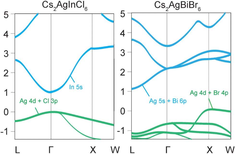 | ||
| Fig. 1 Schematic illustration of direct and indirect band gaps of halide double perovskites. (Left) In the direct band gap HDP Cs2AgInCl6, both valence band maximum (VBM) and conduction band minimum (CBM) are located at the Γ point. The VBM is due to hybridization of Ag-4d and Cl-3p orbitals, whereas the CBM is mainly contributed by In-5s orbitals. (Right) Cs2AgBiBr6 is a typical indirect band gap HDP with the VBM contributed by Ag-5s and Bi-6p orbitals, and the CBM by Ag-4d and Br-4p orbitals. | ||
A direct band gap is characteristic of compounds such as Cs2AgInCl6 and Cs2AgSbCl6, which demonstrate high absorption coefficients and increased PLQYs.37 Cs2AgInCl6 has a band gap of approximately 3.1 eV at the Γ point.37 While the VBM primarily originates from the hybridized antibonding Ag-4d and Cl-3p orbitals, the rest of the valence band is mainly contributed by more localized In-5s and 5p orbitals. The CBM mainly derives from the delocalized In-5s states, which have a large dispersion and a low effective mass.37 The VBM and CBM of Cs2AgInCl6 have the same parity (even) at the Γ point, which makes the direct optical transition forbidden by the selection rule.37
Doping and alloying of the double perovskites with group 13 and group 15 elements are the most common strategies for tuning the band structure and band gap of these materials (Fig. 2). Convenient band gap tuning without changing its nature can be achieved via preparation of solid solution series with isovalent cations. In Cs2AgBiBr6, Bi3+ cation substitution with Sb3+ reduces the band gap in a relatively narrow range from 2.27 eV to 1.80 eV for 0 and 33% of Sb3+, respectively.38 Curiously, the Sb3+ substitution level is limited by the structural stability of the octahedral units and the formation of a secondary phase, revealing some limitations of this approach for band gap tuning.38
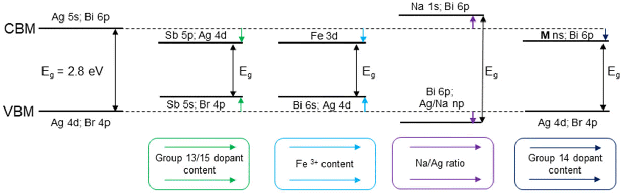 | ||
| Fig. 2 Effect of the substitution on the conduction and valence bands and the band gap in Cs2AgBiBr6 HDPs. | ||
Unlike isovalent substitution that often causes a gradual change in the band structure, aliovalent substitution can introduce new levels and shift the Fermi level. For example, Sn4+ incorporation into the Cs2AgBiBr6 double perovskite matrix results in lowering of the band gap due to the formation of a new band by hybridization of Sn-5s and Bi-6p orbitals.39 As a result, the band gap reduces by 0.2 eV due to lowering of the CBM. Ge4+ incorporation into the Bi site has a similar effect to Sn4+ substitution, but the band gap reduction is smaller, 0.1 eV, because of the smaller radius of the Ge-4s orbital, resulting in a weaker overlap with the Bi-6p orbitals.39
A dramatic band gap narrowing from 3.19 eV to 1.24 eV is reported for Cs2NaInCl6 by introducing Sb5+ doping.40 The authors claim that the [SbCl6]− cluster formation within the crystal lattice generates a localized insertion energy band between the VB and CB. This new level contributes to band gap narrowing as evidenced by strong visible light absorption.40 However, this interpretation is challenged in a recent comment by Xiao, who argues that the observed band gap narrowing is likely due to the formation of a side product Cs4SbIIISbVCl12 rather than the intrinsic properties of the doped Cs2NaInCl6 material.41
Isovalent cations from different groups act similarly to the aliovalent ones and change both the position of the Fermi level and band dispersion. In Cs2AgxNa1−xBiyIn1−yCl6, the band gap decreases from 3.12 eV for y = 0.0005 to 2.68 eV for y = 1.42 The valence band edge shifts to lower energies as the Bi content increases, from 2.66 eV for y = 0 to 1.75 eV for y = 1 with respect to the Fermi level. The conduction band edge also shifts to lower energies as the Bi content increases, following the band gap narrowing. These changes in the band structure are attributed to the introduction of [BiCl6]3− units into the Cs2AgxNa1−xBiyIn1−yCl6 lattice, which break the symmetry and create localized states below the conduction band minimum, thus facilitating light absorption and emission.42
Transition metal (TM) ion incorporation has also been probed as a relatively uncommon yet effective way of band gap engineering in halide perovskites. The band gap of Cs2AgBiBr6 can be reduced from 2.2 eV to 1.8 eV after 25% Ru-doping, as calculated by DFT.43 A new intermediate band, dominated mainly by Ru 4d orbitals, appears within the original band gap of Cs2AgBiBr6. The intermediate band lies below the Fermi level and offers additional transition channels to the conduction band.43 In another example, Cs2AgInxFe1−xCl6 (0 ≤ x ≤ 1), the band gap has been tuned by varying the In content, from 0.21 eV for x = 0 to 0.72 eV for x = 1.44 Both Cs2AgFeCl6 and Cs2AgInCl6 have a direct band gap, while the mixed Cs2AgIn0.76Fe0.24Cl6 phase exhibits an indirect one, requiring a phonon assistance for an electron transition. The CBM, which is composed of In-5s states, remains largely unchanged in the entire composition range.44 However, Fe incorporation changes the VBM from being primarily contributed by Cl-3p and Ag-4d states to Fe-3d and Cl-3p, leading to a drastic change in the band gap even in the presence of small Fe quantities. The band gap changes abruptly initially as the Fe3+ concentration increases, followed by a steadier decrease at high concentrations.44 A similar situation was observed in Cs2AgxNa1−xFeyIn1−yCl6. The direct band gap drops from 3.10 eV for undoped Cs2AgxNa1−xInCl6 to 1.95 eV for Cs2AgxNa1−xFe0.99In0.01Cl6.45 The band gap shows two distinct modes: a slow increase from 1.95 eV to 2.33 eV for y = 0.99–0.50, and a steep rise from 2.33 eV to 3.10 eV for y = 0.50–0.0 (Fig. 3a).45 This nonlinear variation of the band gap depending on the composition commonly referred to as the “bowing effect” can be explained by local distortions in the structure. The non-linearly varying band gap is observed in a wide range of semiconducting alloys, including lead and tin halide perovskites.46–50 Among other factors, local structural relaxations and distortions are shown to be one of the primary reasons for nonlinear changing of the band gap in perovskite systems.49 A solid-state NMR study shows that Fe3+ replaces In3+ in the lattice, forming [FeCl6]3−·[AgCl6]5− domains with different sizes and distribution modes depending on x, growing larger as the Fe3+ concentration increases.51 This leads to the formation of microscopically segregated Fe3+ rich phases in Cs2AgInxFe1−xCl6 (Fig. 3b).51
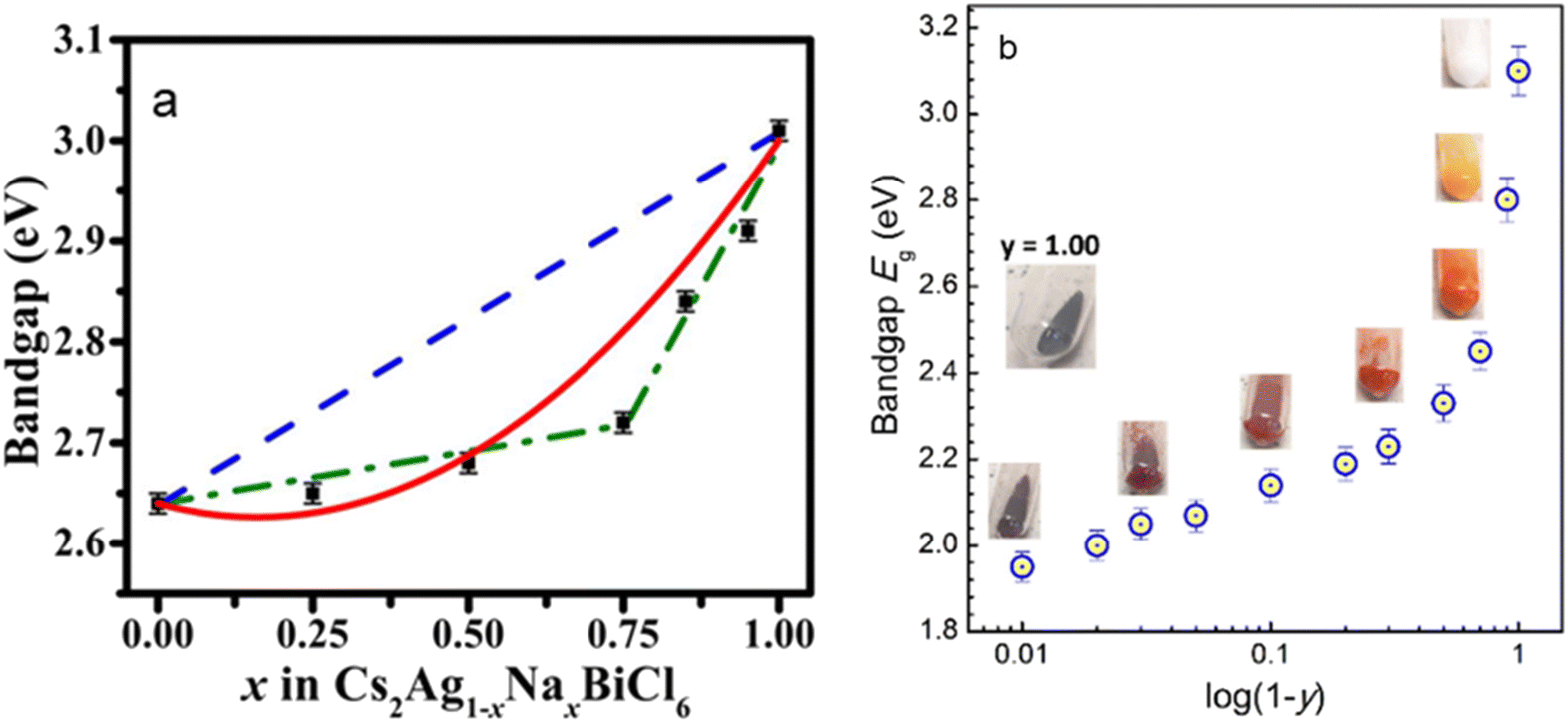 | ||
| Fig. 3 (a) Band gap variation as a function of the Na content in Cs2Ag1−xNaxBiCl6. The black squares are the data points, the dashed blue line shows the band gap predicted by Vegard's law, and the red line is a fit according to the band gap bowing equation. Reproduced from ref. 55 with permission from the American Institute of Physics (AIP). (b) Nonlinear band gap variation in Cs2Ag1−xNaxFeyIn1−yCl6 as a function of the In content (1 − y). Reproduced from ref. 45 with permission from the Royal Society of Chemistry. | ||
Transition metal incorporation into a HDP matrix can also change the nature of the band gap by altering the CBM or VBM. In Cs2AgBiBr6, the substitution of Bi3+ with Fe3+ leads to a red shift of the absorption onset from 2.1 to ≈1 eV due to the lowering of the conduction band minimum by Fe-3d states.52 DFT calculations explained the band gap reduction and predicted a change from an indirect band gap to a direct band gap for high Fe3+ concentrations (x > 0.5). After the incorporation of Fe3+, the VBM is mainly derived from Bi-6s and Ag-4d states, while the CBM has an Fe-3d character.52 The hybridization of Fe-3d and Ag-5s states increases with x, leading to a more dispersed CBM. While the band gap of the pristine compound is indirect, with the VBM and CBM at the Γ and L points, increasing the Fe3+ concentration gradually shifts the CBM to X and then to Γ, resulting in a direct band gap for x > 0.5.52 Similar band gap reduction and valence band change were observed in the Cs2NaBi1−xFexCl6 double perovskite with the incorporation of Fe3+ ions into the Cs2NaBiCl6 lattice.53 The same effect was achieved through doping with another TM cation, Mn2+. In Cs2NaInCl6 doped with Mn2+, a slight increase in the band gap is observed and it varies as 4.08, 4.10, 4.11 and 4.12 eV for 0.2, 0.6, 1.1 and 1.7 at% Mn2+ respectively.54 The increase in the band gap is due to the reduced contribution of In-5s at the conduction band maximum caused by the introduction of Mn-3d states.54
Although the trivalent cation site offers more versatility for substitution, Ag/Na substitution has its own distinct effects on the band structure of HDPs. In Cs2Ag1−xNaxBiCl6, the band gap changes from 2.64 eV to 3.01 eV as Ag+ is replaced with Na+.55 This change originates primarily from the local distortions of the [BiCl6]3− and [AgCl6]5− octahedra, which affect the electronic structure and the interplay between the Ag+/Na+ and Bi3+ sublattices.55 The incorporation of silver ions into the sodium site in Cs2AgxNa1−xBiCl6 not only results in a decrease in the lattice parameter, but also introduces covalency through the Ag–Cl bonds. This leads to a strain in the host crystal structure and a variation of the band gap with composition. The band gap deviates from Vegard's rule and shows a “bowing effect”.55 The VBM is mainly formed by the Ag-4d and Cl-3p atomic orbitals, while the CBM is dominated by the Bi-6p and Cl-3p orbitals. As the silver content increases, the Ag-4d states influence the orbital interactions responsible for forming the valence band edge and shift it closer to the Fermi energy.55 Scanning tunneling spectroscopy studies reveal that the double perovskite alloys form an internal type-I band alignment between the two endmembers, Cs2NaBiCl6 and Cs2AgBiCl6.56 This means that the band gap of an intermediate alloy arises from the lower of the two conduction band edges and the higher of the two valence band edges. This also contributes to the band gap bowing phenomenon.56 The direct band gap of Cs2AgxNa1−xFeyIn1−yCl6 perovskites also changes with the Ag-to-Na ratio x, which can be varied in the range of 0.1–0.2 < x < 0.6–0.7. The band gap decreases from 2.28 eV for x = 0.12 to 1.95 eV for x = 0.50 and shows a linear dependence on the actual Ag content x.45
Overall, doping and alloying offer versatile routes for band gap engineering in HDP materials. From the present data, one can surmise that the “bowing effect” manifests itself depending on the local structure of the double perovskite. A uniform distribution of dopant atoms in the structure is likely to foster a linear change in the band gap by gradually changing the band structure. However, any local domains or inhomogeneities can result in a type-I internal band alignment and introduce nonlinearity into the change of the electronic properties of the HDP materials.
3. HDP photoluminescence
Photoluminescence of HDPs depends strongly on their composition and electronic structure. Pristine, undoped 3D HDPs often exhibit low PLQYs due to a large indirect band gap, as in Cs2AgBiBr6 and Cs2AgBiCl6,10 or parity forbidden transitions, as in Cs2AgInCl6.37 Unlike their 3D counterparts, vacancy-ordered 0D double perovskites (Fig. 4) often demonstrate intrinsic broad band blue-white emission with high PLQYs originating from self-trapped excitons.17,57 For example, the PLQY of the Rb2ZrCl6 phase is 60%.57 The DFT calculations showed that this compound has a direct band gap of 3.59 eV and electronic states highly localized within the [ZrCl6]2− units. These PL properties can be tuned by changing the composition of this compound as Cl− replacement for Br− in the Rb2ZrCl6−xBrx (0 ≤ x ≤ 4) series allowed a 70 nm red shift of the PL peak, while preserving a relatively high PLQY.57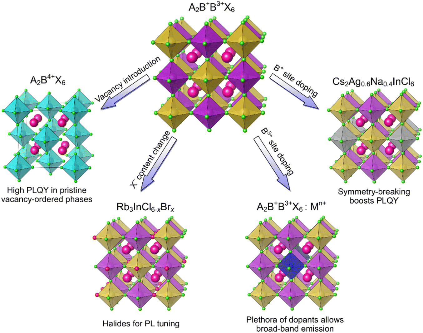 | ||
| Fig. 4 Compositional changes of HDPs for light conversion applications. | ||
While vacancy-ordered HDPs often offer exceptional PL properties, further enhancement can be achieved through RE incorporation. RE3+ cations feature prominent narrow emission bands in specific spectral regions.58,59 Moreover, while many materials undergo thermal quenching of luminescence, the emission of RE3+ originating from f–f transitions shows high thermal stability.58,59 Since the operation of LEDs unavoidably causes device heating, it is vital for phosphors to sustain the efficiency and color of emitted light at elevated temperatures. For example, a high PLQY of 62% and antithermal quenching of PL in the red and IR regions were reported in Cs2NaEr0.4Yb0.6Cl6.60 In this material, a cross relaxation from Er3+ to Yb3+ excited states results in a peak PL intensity at 400 K, showing a synergistic property enhancement by using two different RE cations.60
Although most phosphor converted wLEDs are based on down-conversion of UV or blue radiation from a semiconductor chip by a luminescent material,61 HDPs doped with RE3+ cations offer up-conversion of the IR radiation to visible light. Thus, the pristine Cs2NaErCl6 HDP exhibits a bright green and orange emission upon IR excitation.62 The introduction of Yb3+ cations into the Er3+ sites accentuates and blue shifts the orange emission. Similarly, doping of the Cs2NaErCl6 phase with Tm3+ enhances red emission under 980 nm laser excitation. Efficient up- and down-conversion can be achieved in one material. The Yb3+ and Er3+ co-doped Cs2NaScCl6 HDP up-converts 980 and 1550 nm IR laser radiation into green light and down-converts 365 nm UV lamp radiation into red light.63 Additionally, the material response to the external stimuli depends on the excitation laser power: by increasing the optical power density, the green emission can be redshifted to a yellow one. Multicolor emission achieved in Cs2NaErCl6 and Cs2NaScCl6 samples offers advanced anticounterfeiting technologies.63
Apart from the significant effect of transition metal doping on the electronic structure, described in the first part of this paper, TM cations also serve as common activators for PL applications.64 Naturally, they were probed as luminescence centers for HDPs to achieve a remarkable PL. The Cs2NaBiCl6 double perovskite phosphor demonstrates orange-red emission upon Mn2+ doping.65,66 Noteworthily, a high PLQY (31.6%) and good thermal stability of the emission were achieved by morphology manipulation of the doped material.66 Another crucial application of Cs2NaBiCl6:Mn2+ is radiation detection. A scintillator film based on Cs2NaBiCl6:4.04%Mn2+ nanocrystals has a high light yield, low detection limits, good spatial resolution and X-ray exposure stability.67 Doping of the Cs2NaBiCl6 double perovskite matrix with Mn2+ raises some questions on the dopant location in the crystal structure, since there are no 2+ cation positions in the pristine crystal structure; yet charge balance should be achieved somehow. The issue is complicated with typically low concentrations of the dopant, having a negligible effect on the crystal structure. This matter was addressed by a comprehensive magnetic resonance spectroscopy study,68 which revealed that Mn2+ is located in a nearly perfect octahedral Cl− environment, likely replacing Bi3+.
The reports on ns2 elements (Sb3+, Te4+ and Bi3+) as dopants for halide double perovskites are numerous. These elements are used not only to decrease the band gap, but also to achieve broad-band emission originating in self-trapped exciton recombination. Bright orange emission at 628 nm was reported in Sb3+ doped Rb3BiCl6·0.5H2O.69 In contrast, the introduction of Sb3+ into the Cs2Na(Bi, Sb)Cl6 structure resulted in a PL peak in the blue-green region (480 nm), while the pristine host material emits orange-red light with a peak at 700 nm.70 In Cs2MInCl6:xSb3+, the emission color changes from blue to green for M = Na and M = K, respectively.71 The difference is associated with changes in the crystal structure: the Cs2KInCl6 compound is tetragonal, while Cs2NaInCl6 is cubic.
A remarkable feature of ns2-doped phases is a wide emission range that covers the entire visible spectra. Tunable white light emission from Cs2Zr1−xTexCl6 solid solutions was reported.72 While Cs2TeCl6 has a low PLQY (≈4%), Cs2Zr1−xTexCl6 (x = 0.0021) demonstrates 61.5 and 96.1% PLQYs at 254 and 365 nm excitation, respectively. By doping the Rb2SnCl6 matrix with Bi3+, Te4+, and Sb3+, a single component white emitting phosphor has been prepared.73 This material exhibits bright PL under 365 nm excitation that corresponds to the blue, yellow, and red emission maxima of Bi3+, Te4+, and Sb3+ centers, respectively. The combination of yellow and blue emission produces cold white light and is currently employed in wLEDs61 featuring a Ce3+ doped garnet yellow phosphor74 and a blue emitting InGaN chip.75 Thus, a wLED employing a 370 nm chip and Rb2SnCl6:Bi3+,Te4+ phosphors with optimized composition achieved a 92.2 color rendering index.73
Co-doping of halide double perovskites with various combinations of TM, ns2, and RE cations is a convenient way to achieve multicolor emission (Fig. 5). If energy transfer between various dopants is allowed, additional effects may appear in their optical behavior. Co-doping of the Cs3Cd2Cl7 phase with Mn2+ and Sb3+ resulted in a long afterglow (over 10 s) in the material.76 After studying single Mn2+ and Sb3+ doped Cs3Cd2Cl7, the authors concluded that energy transfer occurs from Cd2+ to Sb3+ and then to Mn2+ states. The orange-yellow emission of Cs3Cd2Cl7:Mn2+,Sb3+ originates in d–d relaxations of the Mn2+ cation.76 It is worth noting that the single Mn2+ doped phase shows a much higher PLQY, compared to the co-doped phase.76 In contrast, Cs2ZnCl4:Mn2+,Sb3+ did not show any evidence of charge transfer: the emission of this phase consists of two separate bands which have different excitation energies. Additionally, time-resolved PL showed a single exponential decay behavior for both Mn2+ and Sb3+ emission.77 Energy transfer between the dopants was observed for the Cs2NaInCl6:RE3+,Sb3+ HDP.78 Cs2NaInCl6:Er3+,Sb3+ emits light in quite separated regions of the spectra – blue and near infrared.78 On the other hand, no infrared emission was reported for Cs2NaInCl6:Er3+,Ho3+,Sb3+ and red emission was assigned to Ho3+ rather than Er3+ cations.79
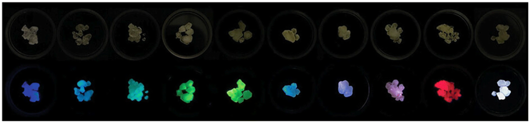 | ||
| Fig. 5 Sb3+ and RE3+ co-doped Cs2NaYCl6 crystals under visible (top) and UV light (365 nm, bottom). Changing the doping level allows tunable emission. Reproduced from ref. 80 with permission from Wiley-VCH GmbH. | ||
Additionally, doping can cause indirect effects on PL as it occurs in the case of Na+ doping on the Ag+ sites in chloride double perovskites. Such doping causes wavefunction symmetry-breaking of the Jahn–Teller distorted AgCl6 octahedra and promotes radiative recombination, which are parity-forbidden in undoped materials.81 This results in a tremendous improvement of the PLQY from STE emission and was demonstrated for the Cs2Ag0.60Na0.40InCl6:Bi3+ double perovskite and confirmed later for many mixed Ag/Na phases.81
Another intriguing case of broadband emission in halide perovskites requires consideration. In the Rb3InCl6−xBrx (x = 0, 2, 3, 4, 6) series, the change of the halogen content allowed tuning of the PL wavelength from 436 nm in pure chloride to 505 nm in pure bromide.82
Thus, halide double perovskites possess great capabilities for solid state lighting. The unsatisfactory efficiency of pristine materials can be extensively improved by various doping strategies. Co-doping with numerous combinations of ns2, TM, and RE cations allows achieving broad-band emission in a single matrix. However, the energy transfer between various co-dopants showed a negative effect on the material PLQY in some cases.
4. Conclusions and outlook
The A2M′+M′′3+X6 double perovskite matrix offers a wide range of compositions as M′′3+ sites can be occupied by group 13–15 elements, transition metals, rare-earth cations, and combinations thereof. This flexibility provides HDPs with a high degree of tunability of physical properties through various doping and alloying strategies. Isovalent substitution in the series of solid solutions is employed to tune the band gap while preserving its nature. On the other hand, aliovalent substitution introduces new bands in the band structure and shifts the Fermi level more dramatically, oftentimes changing the nature of the band gap. This conversion of an indirect band gap material into a direct one can substantially boost its PLQY. Besides the band structure tuning, the introduction of rare earth, transition metal, or main group cations into HDP matrices produces luminescent materials with the dopant ions acting as luminescence centers. The HDP matrix allows combining various activators, for example, RE3+ and Sb3+, to achieve a tunable or broadband emission in a single compound.Despite the tunability of the composition and properties, HDP materials still face notable limitations. For now, photovoltaic applications of HDPs are challenged by the nature and widths of their band gaps. Most of the materials reported to date are chlorides and bromides with intrinsically larger band gaps, while reports on lower band gap iodides are scarce.83 Similar to lead perovskites, organic cations such as methylammonium can be employed for the synthesis of hybrid HDP-inspired materials. However, the reduction of the metal halide polyhedra connectivity and formation of low dimension structures often caused by organic cations harm photovoltaic performance.84
Overall, lead-free HDP materials offer a non-toxic and stable alternative to lead-based perovskites. Doping and alloying of HDP matrices grant them valuable optical properties. Potential applications of HDPs include phosphor-converted LEDs, anti-counterfeiting technologies and IR detection, while further expansion of their application into lasers and ionizing radiation detection fields can be expected.
Data availability
No primary research results, software or code have been included and no new data were generated or analysed as part of this review.Author contributions
Sergei A. Novikov – conceptualization, visualization, writing – original draft, and writing – review and editing. Aleksandra D. Valueva – conceptualization, visualization, writing – original draft, and writing – review and editing. Vladislav V. Klepov – conceptualization, funding acquisition, project administration, validation, resources, supervision, and writing – review and editing.Conflicts of interest
The authors declare no conflict of interest.Acknowledgements
This work was supported by the University of Georgia Department of Chemistry, Franklin College of Arts and Sciences, and the Office of Provost.References
- Y. Zhao, K. Cruse, M. Abdelsamie, G. Ceder and C. M. Sutter-Fella, Matter, 2021, 4, 1801–1831 CrossRef CAS.
- A. Bibi, I. Lee, Y. Nah, O. Allam, H. Kim, L. N. Quan, J. Tang, A. Walsh, S. S. Jang, E. H. Sargent and D. H. Kim, Mater. Today, 2021, 49, 123–144 CrossRef CAS.
- S. Ghosh, H. Shankar and P. Kar, Mater. Adv., 2022, 3, 3742–3765 RSC.
- S. A. Khan, N. Z. Khan, M. Sohail, M. Runowski, X. Xu and S. Agathopoulos, Mater. Today Phys., 2023, 34, 101079 CrossRef CAS.
- A. S. Darsan and A. Pandikumar, Mater. Sci. Semicond. Process., 2024, 174, 108203 CrossRef CAS.
- D. Y. Heo, M. A. Tekalgne and S. Y. Kim, EES Catal., 2024, 2, 94–108 RSC.
- S. Mei, J. Yin, Y. Xing, H. He, H. Gu, J. Xia, W. Zhang, C. Liang, G. Xing and R. Guo, Nano Energy, 2024, 122, 109339 CrossRef CAS.
- E. T. McClure, M. R. Ball, W. Windl and P. M. Woodward, Chem. Mater., 2016, 28, 1348–1354 CrossRef CAS.
- S. J. Zelewski, J. M. Urban, A. Surrente, D. K. Maude, A. Kuc, L. Schade, R. D. Johnson, M. Dollmann, P. K. Nayak, H. J. Snaith, P. Radaelli, R. Kudrawiec, R. J. Nicholas, P. Plochocka and M. Baranowski, J. Mater. Chem. C, 2019, 7, 8350–8356 RSC.
- M. R. Filip, S. Hillman, A. A. Haghighirad, H. J. Snaith and F. Giustino, J. Phys. Chem. Lett., 2016, 7, 2579–2585 CrossRef CAS PubMed.
- F. Ji, G. Boschloo, F. Wang and F. Gao, Sol. RRL, 2023, 7, 2201112 CrossRef CAS.
- J. Nie, H. Li, S. Fang, B. Zhou, Z. Liu, F. Chen, Y. Wang and Y. Shi, Cell Rep. Phys. Sci., 2022, 3, 100820 CrossRef CAS.
- G. Zhang, D. Wang, B. Lou, C.-G. Ma, A. Meijerink and Y. Wang, Angew. Chem., Int. Ed., 2022, 61, e202207454 CrossRef CAS PubMed.
- A. Huang, M. Liu, C.-K. Duan, K.-L. Wong and P. A. Tanner, Inorg. Chem. Front., 2022, 9, 6379–6390 RSC.
- W. Zhuang, H. Liu, Y. Chen, W. Xu, H. Gao, Y. Tian, D. Yao and H. Zhang, Ceram. Int., 2023, 49, 15761–15770 CrossRef CAS.
- W. Zhou, C. Li, T. Wu, R. Liu, Z. Ding, R. Zhang, Y. Yu, P. Han and R. Lu, J. Phys. Chem. Lett., 2023, 14, 8577–8583 CrossRef CAS PubMed.
- K. Zheng, B. Chen, L. Xie, X. Li, B. Lu, M. Wang, Y. Wu, T. Jiang, F. Zhang, X. Li and Y. Wang, Adv. Opt. Mater., 2022, 10, 2101661 CrossRef CAS.
- F. Zhu, Y. Gao, C. Zhao, J. Pi and J. Qiu, ACS Appl. Mater. Interfaces, 2023, 15, 39550–39558 CrossRef CAS PubMed.
- M. Jeevaraj, D. Sivaganesh, S. Saravanakumar, S. A. Bahadur, S. Sudhahar and M. K. Kumar, Opt. Mater., 2023, 143, 114294 CrossRef CAS.
- C. Zhou, Y. Tian, Z. Yuan, H. Lin, B. Chen, R. Clark, T. Dilbeck, Y. Zhou, J. Hurley, J. Neu, T. Besara, T. Siegrist, P. Djurovich and B. Ma, ACS Appl. Mater. Interfaces, 2017, 9, 44579–44583 CrossRef CAS PubMed.
- A. Žukauskas, R. Vaicekauskas and M. Shur, Opt. Express, 2010, 18, 2287–2295 CrossRef PubMed.
- W. Zhang, S. Thapa, Y. Sun, S. Norville, H. Zhu, P. Zhu, G. Wang and W. Qin, Chem. Eng. J., 2021, 423, 130186 CrossRef CAS.
- T. Bai, X. Wang, Z. Wang, S. Ji, X. Meng, Q. Wang, R. Zhang, P. Han, K. Han, J. Chen, F. Liu and B. Yang, Angew. Chem., Int. Ed., 2023, 62, e202213240 CrossRef CAS PubMed.
- F. Igbari, Z.-K. Wang and L.-S. Liao, Adv. Energy Mater., 2019, 9, 1803150 CrossRef.
- L. Lu, X. Pan, J. Luo and Z. Sun, Chem. – Eur. J., 2020, 26, 16975–16984 CrossRef CAS PubMed.
- Y. Wu, X. Li and H. Zeng, Small Struct., 2021, 2, 2000071 CrossRef CAS.
- T. Appadurai, R. Kashikar, P. Sikarwar, S. Antharjanam, B. R. K. Nanda and A. K. Chandiran, Commun. Mater., 2021, 2, 1–16 CrossRef.
- L. Zhang and M. Yuan, Light: Sci. Appl., 2022, 11, 99 CrossRef CAS PubMed.
- T. Wang, D. Zhou, Z. Yu, T. Zhou, R. Sun, Y. Wang, X. Sun, Y. Wang, Y. Shao and H. Song, Energy Mater. Adv., 2023, 4, 0024 CrossRef CAS.
- S. Jin, R. Li, H. Huang, N. Jiang, J. Lin, S. Wang, Y. Zheng, X. Chen and D. Chen, Light: Sci. Appl., 2022, 11, 52 CrossRef CAS PubMed.
- R. Zhang, Z. Wang, X. Xu, X. Mao, J. Xiong, Y. Yang and K. Han, Adv. Opt. Mater., 2021, 9, 2100689 CrossRef CAS.
- S. Li, C. Zhu, J. Wang, Z. Zhang, D. Wang, Y. Chen, D. Zhang, J. Wang and J. Zhang, J. Mater. Chem. C, 2024, 12, 4720–4727 RSC.
- X. Deng, S. Cheng, X. Chen, M. Wang, X. Li, G. Li, D. Zhu, M. Jia, X. Li and Z. Shi, J. Lumin., 2024, 269, 120525 CrossRef CAS.
- Y. Zhang, X. Liu, H. Sun, J. Zhang, X. Gao, C. Yang, Q. Li, H. Jiang, J. Wang and D. Xu, Angew. Chem., Int. Ed., 2021, 60, 7587–7592 CrossRef CAS PubMed.
- X. Cheng, Z. Xie, W. Zheng, R. Li, Z. Deng, D. Tu, X. Shang, J. Xu, Z. Gong, X. Li and X. Chen, Adv. Sci., 2022, 9, 2103724 CrossRef CAS PubMed.
- A. A. Bhat, N. Singh, R. V. Nair, E. Dujardin and J. Sharma, Opt. Mater., 2023, 141, 113937 CrossRef CAS.
- W. Meng, X. Wang, Z. Xiao, J. Wang, D. B. Mitzi and Y. Yan, J. Phys. Chem. Lett., 2017, 8, 2999–3007 CrossRef CAS PubMed.
- S. Yoon, B. Fett, A. Frebel, S. Kroisl, B. Herbig, M. Widenmeyer, B. Balke, G. Sextl, K. Mandel and A. Weidenkaff, Energy Technol., 2022, 10, 2200197 CrossRef CAS.
- P. Sebastiá-Luna, J. Calbo, N. Albiach-Sebastián, M. Sessolo, F. Palazón, E. Ortí and H. J. Bolink, Chem. Mater., 2021, 33, 8028–8035 CrossRef.
- Y. Liu, X. Dai, X. Zeng, X. Yuan, Y. Wang, Y. Song, H. Chen, C. Zhang, Y. Wang, L. Wan, Y. Zou, W. Ning and B. Sun, Adv. Opt. Mater., 2024, 12, 2301576 CrossRef CAS.
- Z. Xiao, Adv. Opt. Mater., 2024, 2302471 CrossRef.
- O. Stroyuk, O. Raievska, A. Barabash, C. Kupfer, A. Osvet, V. Dzhagan, D. R. T. Zahn, J. Hauch and C. J. Brabec, Mater. Adv., 2022, 3, 7894–7903 RSC.
- Z. Zhang, G. Liu, W. Guo, X. Li, Y. Zhang, C. Wu, B. Qu, J. Shi, Z. Chen and L. Xiao, Mater. Adv., 2022, 3, 4932–4937 RSC.
- H. Yin, Y. Xian, Y. Zhang, W. Chen, X. Wen, N. U. Rahman, Y. Long, B. Jia, J. Fan and W. Li, Adv. Funct. Mater., 2020, 30, 2002225 CrossRef CAS.
- O. Stroyuk, O. Raievska, A. Barabash, J. Hauch and C. J. Brabec, J. Mater. Chem. C, 2023, 11, 6867–6873 RSC.
- S.-H. Wei and A. Zunger, Phys. Rev. B: Condens. Matter Mater. Phys., 1989, 39, 3279–3304 CrossRef CAS PubMed.
- W. Shan, W. Walukiewicz, J. W. Ager, E. E. Haller, J. F. Geisz, D. J. Friedman, J. M. Olson and S. R. Kurtz, Phys. Rev. Lett., 1999, 82, 1221–1224 CrossRef CAS.
- J. Wu, W. Walukiewicz, K. M. Yu, J. W. Ager, E. E. Haller, I. Miotkowski, A. K. Ramdas, C.-H. Su, I. K. Sou, R. C. C. Perera and J. D. Denlinger, Phys. Rev. B: Condens. Matter Mater. Phys., 2003, 67, 035207 CrossRef.
- A. Rajagopal, R. J. Stoddard, H. W. Hillhouse and A. K.-Y. Jen, J. Mater. Chem. A, 2019, 7, 16285–16293 RSC.
- S. Khatun, A. Maiti and A. J. Pal, Appl. Phys. Lett., 2020, 116, 012104 CrossRef CAS.
- F. Ji, F. Wang, L. Kobera, S. Abbrent, J. Brus, W. Ning and F. Gao, Chem. Sci., 2021, 12, 1730–1735 RSC.
- H. J. Jöbsis, K. Fykouras, J. W. C. Reinders, J. van Katwijk, J. M. Dorresteijn, T. Arens, I. Vollmer, L. A. Muscarella, L. Leppert and E. M. Hutter, Adv. Funct. Mater., 2023, 2306106 CrossRef.
- R. Udavant, S. Thawarkar, S. Rondiya, A. Shelke, R. Aher, T. G. Ajithkumar, R. W. Cross, N. Y. Dzade and S. Jadkar, Inorg. Chem., 2023, 62, 4861–4871 CrossRef CAS PubMed.
- M. Jeevaraj, D. Sivaganesh, S. Saravanakumar, S. A. Bahadur, S. Sudhahar and M. K. Kumar, Mater. Chem. Phys., 2024, 311, 128569 CrossRef CAS.
- A. C. Dakshinamurthy and C. Sudakar, Appl. Phys. Lett., 2021, 118, 131902 CrossRef.
- S. Dan, A. Maiti, S. Chatterjee and A. J. Pal, J. Phys.: Condens. Matter, 2021, 33, 485701 CrossRef CAS PubMed.
- F. Zhang, Z. Chen, Z. Liu, M. Jia, X. Chen, D. Wu, X. Li and Z. Shi, J. Lumin., 2022, 251, 119150 CrossRef CAS.
- Luminescence: from theory to applications, ed. C. R. Ronda, Wiley-VCH, Weinheim, 2008 Search PubMed.
- Luminescence: Theory and Applications of Rare Earth Activated Phosphors, ed. R. Tiwari, V. Dubey, V. Singh and M. E. Z. Saucedo, De Gruyter, 2021 Search PubMed.
- G. Zhang, P. Dang, H. Lian, H. Xiao, Z. Cheng and J. Lin, Laser Photonics Rev., 2022, 16, 2200078 CrossRef CAS.
- D. A. Steigerwald, J. C. Bhat, D. Collins, R. M. Fletcher, M. O. Holcomb, M. J. Ludowise, P. S. Martin and S. L. Rudaz, IEEE J. Sel. Top. Quantum Electron., 2002, 8, 310–320 CrossRef CAS.
- G. Zhang, P. Dang, H. Lian, S. Huang, W. Yang, Z. Cheng and J. Lin, Adv. Opt. Mater., 2022, 10, 2201220 CrossRef CAS.
- R. Gao, C. Chen, M. Jin, J. Xiang, Z. Li, R. Chen, N. Zhang and C. Guo, Mater. Res. Bull., 2024, 172, 112651 CrossRef CAS.
- V. Rajendran, H. Chang and R.-S. Liu, in Transition metal ion-based phosphors for LED applications, De Gruyter, 2023, ch. 8, pp. 185–220 Search PubMed.
- M. Jeevaraj, S. Sudhahar, P. Devendran, N. Nallamuthu, N. D. Jayram and M. K. Kumar, Mater. Today Commun., 2022, 33, 104715 CrossRef CAS.
- S. Fang, T. Wang, S. He, T. Han, M. Cai, B. Liu, V. I. Korepanov and T. Lang, Phys. Chem. Chem. Phys., 2022, 24, 9866–9874 RSC.
- N. Varnakavi, R. Rajavaram, K. Gupta, P.-R. Cha and N. Lee, Adv. Opt. Mater., 2023, 2301868 Search PubMed.
- A. Karmakar, G. M. Bernard, A. Pominov, T. Tabassum, R. Chaklashiya, S. Han, S. K. Jain and V. K. Michaelis, J. Am. Chem. Soc., 2023, 145, 4485–4499 CrossRef CAS PubMed.
- Z. Jia, P. Gong, M. Chen, Z. Wang, X. Li, Y. Song, S. Zhang, N. Zhang and M. Xia, Inorg. Chem., 2023, 62, 19690–19697 CrossRef CAS PubMed.
- S. Wu, W. Li, J. Hu and P. Gao, J. Mater. Chem. C, 2020, 8, 13603–13611 RSC.
- A. Noculak, V. Morad, K. M. McCall, S. Yakunin, Y. Shynkarenko, M. Wörle and M. V. Kovalenko, Chem. Mater., 2020, 32, 5118–5124 CrossRef CAS PubMed.
- Y. Liu, Y. Wu, Z. Juan, X. Sun, W. Zhang, H. Zeng and X. Li, Adv. Opt. Mater., 2021, 9, 2100815 CrossRef CAS.
- R. Liu, W. Zhang, T. Wen, X. Wen, C. Ding, Z. Li and W. Yan, J. Phys. Chem. Lett., 2022, 13, 11143–11152 CrossRef CAS PubMed.
- G. Blasse and A. Bril, Appl. Phys. Lett., 1967, 11, 53–55 CrossRef CAS.
- S. Nakamura and G. Fasol, The Blue Laser Diode: GaN Based Light Emitters and Lasers, Springer-Verlag, Berlin Heidelberg, 1997 Search PubMed.
- G. Dai, Z. Ma, Y. Qiu and Z. Ma, Inorg. Chem., 2023, 62, 7906–7913 CrossRef CAS PubMed.
- T. Zheng, H. Yang, Y. Liu, Y. Li, Q. Huang, L. Zhang and X. Li, Inorg. Chem., 2023, 62, 17352–17361 CrossRef CAS PubMed.
- S. Saikia, A. Joshi, H. Arfin, S. Badola, S. Saha and A. Nag, Angew. Chem., Int. Ed., 2022, 61, e202201628 CrossRef CAS PubMed.
- J. Nie, B. Zhou, S. Fang, H. Zhong, H. Li and Y. Shi, Chem. Mater., 2022, 34, 6288–6295 CrossRef CAS.
- X.-X. Guo, J.-H. Wei, J.-B. Luo, Z.-L. He, Z.-Z. Zhang, J.-H. Chen and D.-B. Kuang, Adv. Opt. Mater., 2023, 2301914 Search PubMed.
- J. Luo, X. Wang, S. Li, J. Liu, Y. Guo, G. Niu, L. Yao, Y. Fu, L. Gao, Q. Dong, C. Zhao, M. Leng, F. Ma, W. Liang, L. Wang, S. Jin, J. Han, L. Zhang, J. Etheridge, J. Wang, Y. Yan, E. H. Sargent and J. Tang, Nature, 2018, 563, 541–545 CrossRef CAS PubMed.
- X. Liu, C. Zhang, Y. Cao, Y. Wang, L. Peng, J. Chen and J. Lin, Mater. Today Chem., 2023, 29, 101459 CrossRef CAS.
- P. Vishnoi, R. Seshadri and A. K. Cheetham, J. Phys. Chem. C, 2021, 125, 11756–11764 CrossRef CAS.
- W. Fu, H. Chen and A. K.-Y. Jen, Mater. Today Nano, 2021, 14, 100117 CrossRef CAS.
Footnote |
| † These authors contributed equally. |
| This journal is © The Royal Society of Chemistry 2024 |