
Two-dimensional MBenes with ordered metal vacancies for surface-enhanced Raman scattering†
Leilei
Lan
ab,
Xingce
Fan
 b,
Caiye
Zhao
a,
Juan
Gao
a,
Zhongwei
Qu
a,
Wenzhe
Song
b,
Haorun
Yao
b,
Mingze
Li
b and
Teng
Qiu
*bc
b,
Caiye
Zhao
a,
Juan
Gao
a,
Zhongwei
Qu
a,
Wenzhe
Song
b,
Haorun
Yao
b,
Mingze
Li
b and
Teng
Qiu
*bc
aSchool of Mechanics and Optoelectronic Physics, Anhui University of Science and Technology, Huainan 232001, China
bSchool of Physics, Southeast University, Nanjing 211189, China. E-mail: tqiu@seu.edu.cn
cCenter for Flexible RF Technology, Frontiers Science Center for Mobile Information Communication and Security, Southeast University, Nanjing 210096, China
First published on 6th January 2023
Abstract
As an emerging class of two-dimensional (2D) materials, MBenes show enormous potential for optoelectronic applications. However, their use in molecular sensing as surface-enhanced Raman scattering (SERS)-active material is unknown. Herein, for the first time, we develop a brand-new high-performance MBene SERS platform. Ordered vacancy-triggered highly sensitive SERS platform with outstanding signal uniformity based on a 2D Mo4/3B2 MBene material was designed. The 2D Mo4/3B2 MBene presented superior SERS activity to most of the semiconductor SERS substrates, showing a remarkable Raman enhancement factor of 3.88 × 10⁶ and an ultralow detection limit of 1 × 10⁻⁹ M. The underlying SERS mechanism is revealed from systematic experiments and density functional theory calculations that the ultrahigh SERS sensitivity of 2D Mo4/3B2 MBene is derived from the efficient photoinduced charge transfer process between MBene substrates and adsorbed molecules. The abundant electronic density of states near the Fermi level of 2D Mo4/3B2 MBene enables its Raman enhancement by a factor of 100![[thin space (1/6-em)]](https://www.rsc.org/images/entities/char_2009.gif) 000 times higher than that of the bulk MoB. Consequently, the 2D Mo4/3B2 MBene could accurately detect various trace chemical analytes. Moreover, with ordered metal vacancies in the 2D Mo4/3B2 MBene, uniform charge transfer sites are formed, resulting in an outstanding signal uniformity with a relative standard deviation down to 6.0%. This work opens up a new horizon for the high-performance SERS platform based on MBene materials, which holds great promise in the field of chemical sensing.
000 times higher than that of the bulk MoB. Consequently, the 2D Mo4/3B2 MBene could accurately detect various trace chemical analytes. Moreover, with ordered metal vacancies in the 2D Mo4/3B2 MBene, uniform charge transfer sites are formed, resulting in an outstanding signal uniformity with a relative standard deviation down to 6.0%. This work opens up a new horizon for the high-performance SERS platform based on MBene materials, which holds great promise in the field of chemical sensing.
1. Introduction
As a powerful molecular fingerprinting technique with ultra-high sensitivity, non-destructiveness, and label-free detection, surface-enhanced Raman scattering (SERS) has been widely applied in environmental science, biomedicine, molecular analysis, and catalytic mechanism exploration.1–5 Normally, there are two widely accepted SERS enhancement mechanisms, the electromagnetic mechanism (EM) and the chemical mechanism (CM). The former mainly originates from a magnifying local electromagnetic field depending on localized surface plasmon resonance (LSPR), while the latter benefits from the charge transfer (CT) between the substrates and the adsorbed molecules.4,5 In the SERS measurement, substrate materials play an important role. Traditionally, EM-based noble metals (i.e., Au and Ag) have been dominant as SERS-active materials because of their ultra-high sensitivity even at single-molecule level detection. Nevertheless, some inevitable shortcomings including expensive price, poor signal uniformity, lack of stability, and complicated “hotspots” regulation, greatly restrict the large-scale application of noble metal SERS substrates. In contrast, noble-metal-free materials have the advantages of abundant sources, tunable band structure, good chemical stability, superior biocompatibility, and unique selectivity to target molecules,6,7 which could effectively make up for the shortcomings of noble metals and greatly broaden the application of SERS.Recently, the discovery of CM-based two-dimensional (2D) SERS materials opens a new prospect for SERS research. 2D materials possess atomically flat surfaces, large specific surface areas, and insufficient coordination number of surface atoms, making it more likely that surface atoms and adsorbed molecules are combined and further form uniformly distributed surface complexes, which induce efficient photoinduced charge transfer (PICT) process and good signal uniformity.8 So far, a series of 2D SERS-active materials, including graphene,9 transition metal dichalcogenides,8,10 transition metal oxides,11,12 metal–organic frameworks,13 and transition metal carbides/nitrides (MXenes)14,15 have been developed. To further improve their SERS performance, some enhancement strategies such as heterojunction engineering,16 phase transition,10 amorphization treatment,12 defect engineering,17 molecular enrichment,18 and thickness adjustment19 have been explored. Among them, defect engineering is widely used in the research of 2D materials, which provides an effective strategy for the activation and promotion of intrinsic SERS activity. In general, defect engineering breaks the periodic arrangement of atoms, producing point defects or higher dimensional disorder.20 The introduction of defects in 2D materials would change their surface properties, band structures, and density of states (DOS), leading to strong surface interactions, light-trapping capability, or charge transport efficiency, bringing about a direct effect on the SERS performance of 2D materials.21 For example, Zhao et al. demonstrated that ultrathin 2D nanostructures with surface defects could be advantageous in promoting SERS sensitivity.11 Seo et al. reported that single-atom vanadium-doped 2D ReSe2 platform could achieve attomolar level molecular sensing capability.22 Nb, Re dual-doped WSe2 exhibits ultra-high SERS sensitivity with a femtomolar level detection limit.23 However, since these defects are usually either produced inadvertently or formed in macroscopic processes, leading their types and extents are not highly controlled. The disorder defects with uneven distribution can improve the SERS sensitivity but cause poor signal uniformity. Therefore, large-scale control of the ordered defects at the atomic level is of great significance for simultaneously improving the SERS sensitivity and signal uniformity of 2D materials.
As an emerging class of 2D materials, MBenes (transition metal borides) have been theoretically predicted first and experimentally synthesized in the past few years.24–31 In general, MBenes are the derivative of ternary or quaternary MAB phases (where M is an early transition metal, A is an A-group element, and B is a boron element), which possess diverse structures and stoichiometries. Thus far, some types of MBenes, such as MoB,26 TiB,27 CrB,29 and ZrB2,30 have been synthesized by selective etching of element A from their MAB phases. These 2D MBenes featuring excellent electrical conductivity, large surface areas, high mechanical strength/stability, and outstanding thermal conductivity, have been extensively studied in the fields of batteries, catalysts, and biomedicine.24,28,30,31 Especially, similar to the SERS-active MXene materials, MBenes show metallic behavior, which may produce an efficient PICT process between the Fermi level of MBenes and the molecular level of the probe molecules. Moreover, MBenes possess multiple types of crystallographic arrangements and structural transformations, making them more likely to optimize their SERS performance. These properties inspired us to further study 2D MBene materials as they may become an innovative SERS platform.
Herein, ordered vacancy-triggered highly sensitive MBene-based SERS substrate with superior signal uniformity was developed. 2D Mo4/3B2 MBene with ordered metal vacancies was fabricated by selectively etching both the Al and Y atoms from an in-plane chemically ordered (Mo2/3Y1/3)2AlB2. It is demonstrated that 2D Mo4/3B2 Mbene could be used as a SERS-active material, which has not been reported before. Furthermore, we verified that high SERS activity of 2D Mo4/3B2 Mbene substrate was achieved based on the efficient PICT process between the probe molecules and MBene substrates. Compared with bulk MoB, 2D Mo4/3B2 MBene has more abundant DOS near the Fermi level, thereby improving the SERS sensitivity by up to 100000 times. Consequently, 2D Mo4/3B2 MBene could accurately detect various chemical analytes at the trace level. In addition, 2D Mo4/3B2 MBene substrate also shows excellent air-stability (over one month), good signal uniformly with a relative standard deviation (RSD) of 6.0%, and superior quantitative analysis ability with a coefficient of determination R2 of 0.996, which are essential for the practical applications. Our work enriches the diversity of SERS-active materials and may inspire more researchers to explore other 2D MBenes with excellent SERS performance.
2. Results and discussion
2.1 Synthesis and characterization of the 2D Mo4/3B2 MBene
2D Mo4/3B2 MBene was synthesized by a two-step chemical exfoliation process (Fig. 1a). Firstly, hydrofluoric acid (HF) was used to etch Al and Y atoms from (Mo2/3Y1/3)2AlB2. The Mo4/3Y2/3AlB2 is a structure with space group R![[3 with combining macron]](https://www.rsc.org/images/entities/char_0033_0304.gif) m (no. 166), which displays the characteristic in-plane chemical order of Mo and Y and Kagoméordering of the Al atoms.32 Then, etched MBene powder was further delaminated in tetrabutylammonium hydroxide (TBAOH) aqueous solution to reduce the vertical dimension. Because of the ordered arrangements of Mo and Y atoms in the original (Mo2/3Y1/3)2AlB2 MAB phase, highly ordered metal vacancies are formed after the selective removal of Y atoms.33–35 The preparation methods are detailed in the experimental section. Fig. 1b shows the XRD patterns of (Mo2/3Y1/3)2AlB2 MAB phase and Mo4/3B2 MBene, in which all the diffractive peaks belonging to the MAB phase disappeared completely, and a new broadened (00l) peak at 7.3° (d-spacing = 1.21 nm) appeared, implying the successful synthesis of 2D MBene.33 This low-angled (00l) peak is usually observed in 2D MXenes prepared by the HF-etched MAX phase.36,37 The element composition and chemical states of (Mo2/3Y1/3)2AlB2 MAB phase and 2D Mo4/3B2 MBene were investigated using X-ray photoelectron spectroscopy (XPS). In the survey XPS survey spectra (Fig. 1c), the photoemission of Mo, B, Al, Y, O, and C elements was observed in the (Mo2/3Y1/3)2AlB2 MAB phase. After the HF etching treatment, the photoemission from the Y 3p and Al 2p orbitals disappeared. The removal of Al atoms was further confirmed by the high-resolution XPS spectrum of Al 2p (Fig. 1d). The XPS results indicate that the Y and Al atoms were effectively removed from the (Mo2/3Y1/3)2AlB2 MAB phase. In addition, the surface terminations of the -O, -OH, and -F functional groups were also observed on 2D Mo4/3B2. In Fig. 1e, the Mo 3d photoemission spectrum of 2D Mo4/3B2 MBene can be fitted with four pairs of deconvoluted peaks in the range of 226.0 to 237.0 eV, which are attributed to Mo-B (229.3, 232.5 eV), Mo4+ (230.8, 233.9 eV), Mo5+ (231.6, 234.8 eV) and Mo6+ (232.6, 235.8 eV). The Raman spectrum of 2D Mo4/3B2 MBene was measured, as shown in Fig. 1f, where three observed Raman peaks at 240, 338, and 815 cm−1 are assigned to molybdenum boride.38,39 The Raman peaks at 240 and 338 cm−1 originate from the E1g and E12g vibration modes of molybdenum boride and the peak at 815 cm−1 is ascribed to the vibration mode of the Mo–B band. Fig. 1g shows the UV-vis absorption spectrum of 2D Mo4/3B2 MBene dispersion, in which, a distinct absorption peak at ∼215 nm was observed and ascribed to the presence of surface functional groups.14 The inset of Fig. 1g shows a photograph of 2D Mbene dispersion, which appears in brown color and is accompanied by an obvious Tyndall effect.
m (no. 166), which displays the characteristic in-plane chemical order of Mo and Y and Kagoméordering of the Al atoms.32 Then, etched MBene powder was further delaminated in tetrabutylammonium hydroxide (TBAOH) aqueous solution to reduce the vertical dimension. Because of the ordered arrangements of Mo and Y atoms in the original (Mo2/3Y1/3)2AlB2 MAB phase, highly ordered metal vacancies are formed after the selective removal of Y atoms.33–35 The preparation methods are detailed in the experimental section. Fig. 1b shows the XRD patterns of (Mo2/3Y1/3)2AlB2 MAB phase and Mo4/3B2 MBene, in which all the diffractive peaks belonging to the MAB phase disappeared completely, and a new broadened (00l) peak at 7.3° (d-spacing = 1.21 nm) appeared, implying the successful synthesis of 2D MBene.33 This low-angled (00l) peak is usually observed in 2D MXenes prepared by the HF-etched MAX phase.36,37 The element composition and chemical states of (Mo2/3Y1/3)2AlB2 MAB phase and 2D Mo4/3B2 MBene were investigated using X-ray photoelectron spectroscopy (XPS). In the survey XPS survey spectra (Fig. 1c), the photoemission of Mo, B, Al, Y, O, and C elements was observed in the (Mo2/3Y1/3)2AlB2 MAB phase. After the HF etching treatment, the photoemission from the Y 3p and Al 2p orbitals disappeared. The removal of Al atoms was further confirmed by the high-resolution XPS spectrum of Al 2p (Fig. 1d). The XPS results indicate that the Y and Al atoms were effectively removed from the (Mo2/3Y1/3)2AlB2 MAB phase. In addition, the surface terminations of the -O, -OH, and -F functional groups were also observed on 2D Mo4/3B2. In Fig. 1e, the Mo 3d photoemission spectrum of 2D Mo4/3B2 MBene can be fitted with four pairs of deconvoluted peaks in the range of 226.0 to 237.0 eV, which are attributed to Mo-B (229.3, 232.5 eV), Mo4+ (230.8, 233.9 eV), Mo5+ (231.6, 234.8 eV) and Mo6+ (232.6, 235.8 eV). The Raman spectrum of 2D Mo4/3B2 MBene was measured, as shown in Fig. 1f, where three observed Raman peaks at 240, 338, and 815 cm−1 are assigned to molybdenum boride.38,39 The Raman peaks at 240 and 338 cm−1 originate from the E1g and E12g vibration modes of molybdenum boride and the peak at 815 cm−1 is ascribed to the vibration mode of the Mo–B band. Fig. 1g shows the UV-vis absorption spectrum of 2D Mo4/3B2 MBene dispersion, in which, a distinct absorption peak at ∼215 nm was observed and ascribed to the presence of surface functional groups.14 The inset of Fig. 1g shows a photograph of 2D Mbene dispersion, which appears in brown color and is accompanied by an obvious Tyndall effect.
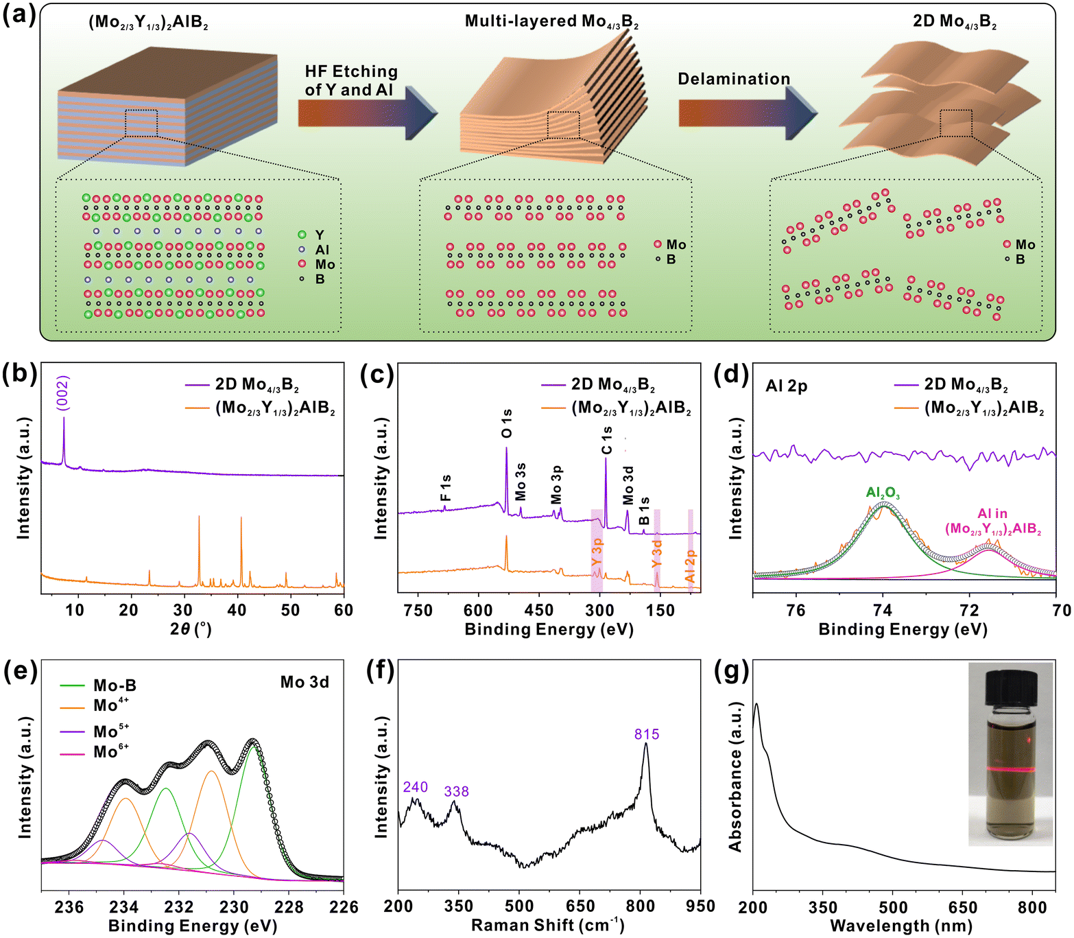 | ||
| Fig. 1 Synthesis and characterization of 2D Mo4/3B2 MBene. (a) Schematics of the synthesis of 2D Mo4/3B2 MBene by a two-step chemical exfoliation process. (b and c) XRD patterns and XPS spectra of (Mo2/3Y1/3)2AlB2 MAB phase and 2D Mo4/3B2 MBene. (d and e) Al 2p and Mo 3d XPS spectra of 2D Mo4/3B2 MBene. (f) Raman spectrum of 2D Mo4/3B2 MBene. (g) UV-vis absorption spectrum of 2D Mo4/3B2 MBene. Inset: a photograph of 2D MBene dispersion. | ||
Scanning electron microscope (SEM), transmission electron microscope (TEM), and atomic force microscope (AFM) were used to examine the sample morphologies. The SEM image of (Mo2/3Y1/3)2AlB2 is shown in Fig. 2a, in which a 3D particle-like structure with several micrometers is observed. After the HF etching treatment, the compact layers are expanded and the multi-layered morphology is formed (Fig. 2b and c). Furthermore, the few-layered structure of delaminated 2D Mo4/3B2 MBene with a lateral size of several hundred nanometers is observed (Fig. 2d), which is similar to the morphologies of typical MXenes.14,36 The AFM image and the corresponding line profile of the few-layered Mo4/3B2 MBene are presented in Fig. 2e and f, further revealing the 2D feature of Mo4/3B2 MBene with a thickness of only ∼4 nm. The SEM image and the corresponding elemental mapping images of the 2D Mo4/3B2 MBene substrate are shown in Fig. 2g, where a smooth morphology of the 2D Mo4/3B2 MBene is observed and the Mo, B, F, and O elements are homogeneously distributed in the sample.
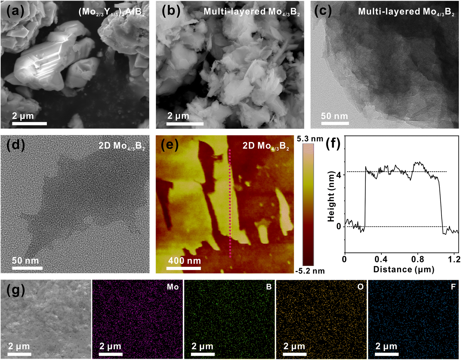 | ||
| Fig. 2 Characterizations of the surface morphologies of MAB, multi-layered, and 2D Mo4/3B2 MBenes. (a and b) SEM images of (Mo2/3Y1/3)2AlB2 and multi-layered Mo4/3B2 MBene. (c and d) TEM images of multi-layered and 2D Mo4/3B2 MBenes. (e) AFM image of 2D Mo4/3B2 MBene. (f) Line profile across the dashed line in the image (e). (g) SEM image and the corresponding elemental mapping images of the 2D Mo4/3B2 MBene substrate. | ||
2.2 SERS performance of the 2D Mo4/3B2 MBene substrate
The SERS performance of 2D Mo4/3B2 MBene was investigated by adopting Rhodamine 6G (R6G) as a probe molecule under the illumination of 532 nm. In the Raman spectrum of R6G (1 × 10⁻⁶ M) adsorbed on 2D Mo4/3B2 MBene (Fig. 3a), four characteristic Raman peaks located at P1 (612 cm−1), P2 (773 cm−1), P3 (1360 cm−1), and P4 (1650 cm−1) can be clearly observed, among which, P1 and P2 are assigned to the in-plane and out-of-plane bending modes of the aromatic C–H, respectively, and P3 and P4 correspond to the stretching vibrations of the aromatic C–C.40 While no Raman signal of R6G can be observed on bare Si, excluding the Raman enhancement effect of the bare Si substrate. It is for the first time to demonstrate 2D Mo4/3B2 MBene as a SERS-active material. The detection limit was evaluated by immersing 2D Mo4/3B2 MBene substrates into R6G solutions with different concentrations (1 × 10⁻⁴ to 1 × 10⁻⁹ M) (Fig. 3b). The Raman peaks of R6G can still be detected even at a concentration of as low as 1 × 10⁻⁹ M, indicating that 2D Mo4/3B2 MBene is an ultrasensitive SERS platform. The corresponding Raman enhancement factor (EF) was estimated to be 3.88 × 10⁶ at the concentration of 1 × 10⁻⁹ M, which is comparable to those reported for high-performance semiconducting or even noble metal SERS platforms (Table S1 in the ESI†).9,12,14,15,41–50 Detailed calculation of the Raman EF is shown in Section S1 in the ESI.†Fig. 3c presents the working curve of the Raman intensity with R6G concentration in the logarithmic scale. A saturated region is distinguished at high R6G concentrations (>1 × 10⁻⁶ M). Besides, the working curve of the Raman intensity versus R6G concentration was fitted as a linear function (R2 = 0.996) over the concentration range of 1 × 10⁻⁶ M to 1 × 10⁻⁹ M, which laid the foundation for the potential application of quantitative detection. Next, 30 random points were tested on the 2D Mo4/3B2 MBene substrate (Fig. 3d) to investigate their SERS signal uniformity. By monitoring the Raman intensities of peak P1, the RSD was calculated to be 6.0% (Fig. 3e), which is much lower than those of the tantalum oxide with disordered oxygen vacancies (13.5%),46 plasmonic gold nanorods (22%),51 and atomically thin TaSe2 film (11.8%).47 The relatively low RSD value proves the excellent signal uniformity of 2D Mo4/3B2 MBene. Generally, SERS substrates require the homogeneity of CT sites or plasmonic “hotspots” to generate superior signal uniformity. In this work, 2D Mo4/3B2 MBene substrates showed smooth surface morphology (Fig. 2g and Fig. S1 in the ESI†) and the ordered metal vacancy sites, which guarantee the homogeneity of the CT sites and enable ideal SERS signal uniformity. The 2D Mo4/3B2 MBene also possesses high air stability and its SERS activity remains virtually unchanged after one month of storage in air (Fig. 3f). The 2D Mo4/3B2 MBene substrate can also be used to detect a series of chemicals, such as fuchsin acid (FA), crystal violet (CV), methylene blue (MB), malachite green (MG), and rhodamine B (RhB), and brilliant green (BG) (Fig. 4), among which CV and MG are both the banned fish drugs for their adverse effects on the health and the environment.8 The detection limits of FA, CV, MB, MG, RhB, and BG were tested as low as 1 × 10⁻⁷, 1 × 10⁻⁸, 1 × 10⁻⁶, 1 × 10⁻⁸, 1 × 10⁻⁶, and 1 × 10⁻⁷ M, respectively, demonstrating the enormous potential of 2D Mo4/3B2 MBene in practical applications. In short, all the results clearly certify that the 2D Mo4/3B2 MBene substrate is an innovative and high-performance SERS platform.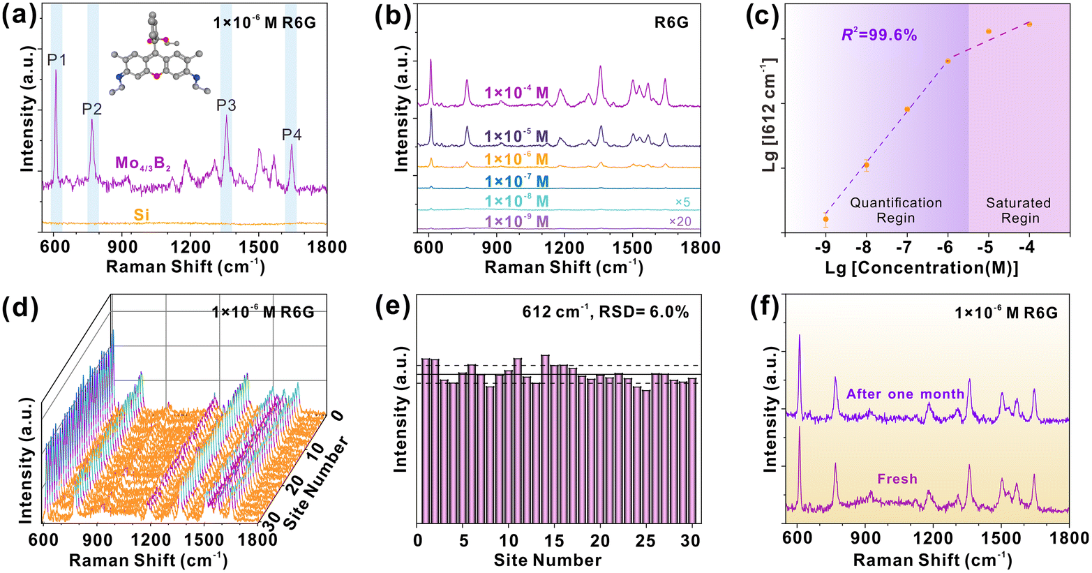 | ||
| Fig. 3 SERS performance of 2D Mo4/3B2 MBene substrate. (a) Raman spectra of R6G (1 × 10⁻⁶ M) adsorbed on bare Si and 2D Mo4/3B2 MBene substrates. (b) Raman spectra of R6G at different concentrations (1 × 10⁻⁴ to 1 × 10⁻⁹ M) adsorbed on 2D Mo4/3B2 MBene substrates. (c) The logarithm of the integral Raman intensity at 612 cm−1 as a function of molecular concentration, and corresponding fitting curves. (d) Raman spectra of R6G (1 × 10⁻⁶ M) acquired from 30 random sites on the 2D Mo4/3B2 MBene substrate. (e) The intensity columns of 612 cm−1 peaks derived from (d). (f) Raman spectra of R6G (1 × 10⁻⁶ M) acquired on 2D Mo4/3B2 substrates before and after storing in the air for one month. | ||
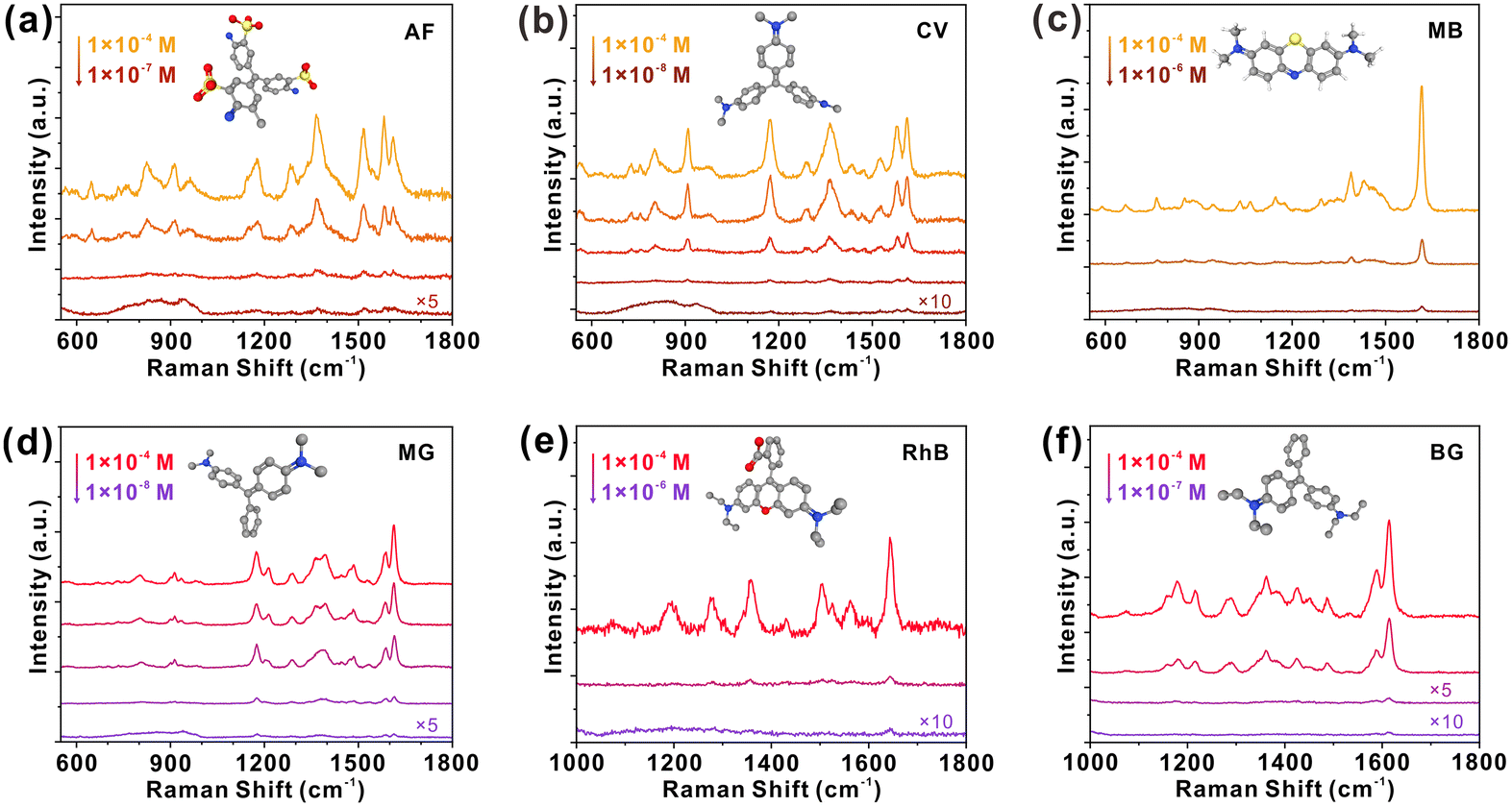 | ||
| Fig. 4 Raman spectra of the detected chemicals by using 2D Mo4/3B2 MBene SERS substrates. Raman spectra of (a) AF, (b) CV, (c) MB, (d) MG, (e) RhB, and (f) BG molecules with different concentrations adsorbed on the 2D Mo4/3B2 MBene substrates. | ||
2.3 Raman enhancement mechanism of 2D Mo4/3B2 MBene substrate
To reveal the Raman enhancement mechanism of 2D Mo4/3B2 MBene, experiments and density functional theory (DFT) calculations were performed. Generally, EM contribution originates from the enhanced local electromagnetic field, which is generated by the LSPR effect.43 However, the LSPR band was not observed in the UV-vis absorption spectrum (Fig. 1g) and the planar surface morphologies of 2D Mo4/3B2 MBene substrates (Fig. 2g and Fig. S1 in the ESI†) should not induce LSPR effect as well, suggesting the EM mechanism can be excluded. Therefore, we speculated that the underlying Raman enhancement mechanism of 2D Mo4/3B2 MBene should be CM-dominated. Compared with the UV-vis absorption spectrum of R6G, the absorption peak of Mo4/3B2-R6G shifts (Fig. 5a), indicating the chemisorption of R6G on 2D Mo4/3B2 surface and the CT behavior at the Mo4/3B2-R6G interface.44 The shifted absorption band of R6G originates from the strong dipole interaction and the quasi-covalent bond interaction between Mo4/3B2 MBene and R6G, which could offer additional routes of charge exchange and greatly increase the Raman scattering cross-section of the adsorbed molecules consequently. A similar phenomenon could also be observed in CV-Mo4/3B2 system (Fig. S2 in the ESI†). Fig. 5b shows the photoluminescence (PL) spectra of R6G, Mo4/3B2, and Mo4/3B2-R6G, where the PL quenching of R6G was observed upon the addition of Mo4/3B2. The quenched PL evidences the efficient CT process between R6G and 2D Mo4/3B2 MBene.47 Besides, 2D Mo4/3B2 MBene does not show PL emission, which provides an ideal SERS platform with a weak background (Fig. S3 in the ESI†). The CT degree of R6G (1 × 10⁻⁶ M) on 2D Mo4/3B2 MBene was estimated to be 0.64, further indicating the CM-dominated feature of this system.11 For the detailed calculations of the CT degree please refer to section S2 in the ESI.† Furthermore, the electronic band structure and the DOS of 2D Mo4/3B2 MBene are shown in Fig. 5c and Fig. S4 in the ESI† respectively, confirming its metallic character. Metallic Mo4/3B2 shows abundant electronic DOS near the Fermi level such that the possible PICT processes would occur between the Fermi level of Mo4/3B2 MBene and the molecule energy levels. Based on the DFT calculations (Fig. 5d), the Fermi level of Mo4/3B2 is located at −4.19 eV with respect to the vacuum level. Taking R6G as a probe molecule, its highest occupied molecule orbital (HOMO) and lowest unoccupied molecule orbital (LUMO) levels are located at −5.70 eV and −3.40 eV, respectively. In general, the polarization tensor (α) can be expressed as α = A + B + C, where A term represents the contributions from the resonance Raman scattering, and B and C terms are relevant to the substrate-to-molecule and molecule-to-substrate CT transitions. As shown in Fig. 5e, the molecular resonance (A-term) would be induced under laser excitation of 532 nm because the energy gap between the HOMO and LUMO levels of the R6G molecule (2.30 eV) is close to the incident photon energy (2.33 eV). It is found that the Raman intensities of R6G (1 × 10⁻⁵ M) adsorbed on Mo4/3B2 MBene under the excitation of 633 nm (1.96 eV) is much lower than that under the excitation at 532 nm (Fig. 5f), which is likely caused by the mismatch between the excitation laser of 633 nm and the HOMO–LUMO energy gap of the molecule (Fig. S5 in the ESI†).46 Additionally, the PICT processes from the Fermi level of MBene to the LUMO of R6G (B-term), and from the HOMO of R6G to the Fermi level of MBene (C-term) are allowed (Fig. 5e). These PICT processes would borrow intensities from the nearby molecular resonance through the Herzberg–Teller vibronic coupling, magnifying the Raman scattering cross-section of molecule consequently.52 Plasmon-free SERS substrates have unique molecular selectivity.16,53 Furthermore, taking 4-mercaptopyridine (4-MPy) as a probe molecule, its HOMO and LUMO levels are located at −9.7 eV and −5.6 eV, respectively.54 Under the excitation of 532 nm laser (2.33 eV), the molecular resonance is ruled out (the energy gap between HOMO and LUMO of 4-MPy is ∼4.1 eV), the PICT process from the HOMO of 4-MPy to the Fermi level of MBene is not allowed (Fig. S6 in the ESI†). Only the PICT process between the Fermi level of MBene and the LUMO of 4-MPy could occur. Therefore, the 4-MPy molecule adsorbed on 2D Mo4/3B2 showed a poor SERS signal (Fig. S7 in the ESI†). This selective Raman enhancement further demonstrates that the SERS mechanism of 2D Mo4/3B2 is CM-dominated.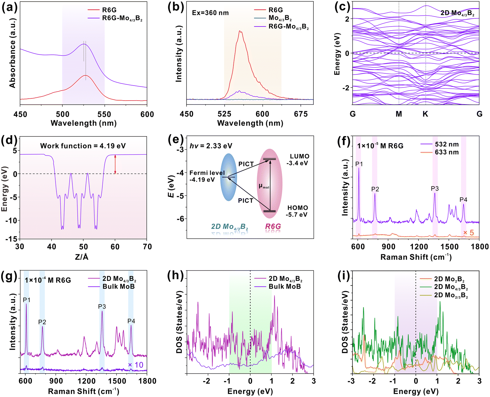 | ||
| Fig. 5 Raman enhancement mechanism of 2D Mo4/3B2 MBene substrate. (a) UV-vis absorption spectra of R6G and Mo4/3B2-R6G. (b) PL spectra of R6G, Mo4/3B2 and R6G-Mo4/3B2. (c and d) The DFT calculations of electronic band structure and work function of 2D Mo4/3B2. (e) The schematic energy level diagram of the Mo4/3B2-R6G system under the illumination of 532 nm (2.33 eV). (f) Raman spectra of R6G (1 × 10⁻⁵ M) adsorbed on 2D Mo4/3B2 measured using the laser at 532 and 633 nm wavelengths. (g) Raman spectra of R6G (1 × 10⁻⁴ M) adsorbed on bulk MoB and 2D Mo4/3B2. (h) The DFT calculations of the DOS of bulk MoB and 2D Mo4/3B2. (i) The DFT calculations of the DOS of 2D Mo2B2 and Mo4/3B2 and Mo2/3B2. | ||
To further understand the efficient PICT processes in Mo4/3B2-molecule system, the Raman spectra and intensity columns of R6G (1 × 10⁻⁴ M) collected on bulk MoB and 2D Mo4/3B2 Mbene are shown in Fig. 5g and Fig. S8, respectively, in the ESI.† The characterizations of bulk MoB are shown in Fig. S9 and S10 in the ESI.† Notably, the SERS performance of 2D Mo4/3B2 MBene is superior to that of bulk MoB. The enhanced Raman peak P1 of R6G on 2D Mo4/3B2 MBene shows ∼116 times higher intensity than that on bulk MoB. Furthermore, the lowest detectable concentration of R6G on 2D Mo4/3B2 MBene is 1 × 10⁻⁹ M (Fig. 3b), which is 5 orders of magnitude lower than that of bulk MoB (1 × 10⁻⁴ M, Fig. S11 in the ESI†). Other molecules, such as CV and MG, adsorbed on 2D Mo4/3B2 MBene were also observed with stronger SERS intensities compared to bulk MoB (Fig. S12, in the ESI†). DFT calculations were conducted to explain why the 2D Mo4/3B2 MBene shows superior SERS activity to the bulk MoB. According to Fermi's golden rule, the electron transition probability can be described as  , in which ħ is the reduced Planck constant, |a〉 and |b〉 are the initial and final states for the charge transition, M is the interaction operator of the two states, and gb is the DOS of the final state.52 Therefore, plenty of allowed energy states near the Fermi level will give rise to a high electron transition probability between the adsorbed molecules and the SERS substrates. As shown in Fig. 5h, 2D Mo4/3B2 MBene possesses a higher electronic DOS value near the Fermi level than that of the bulk MoB. The larger DOS value is beneficial to the improvement of the electron transition probability rate, leading to a remarkable Raman enhancement effect on the 2D Mo4/3B2 MBene. Previous studies have demonstrated that vacancies play an important role in enhancing the non-noble-metal SERS effect.55,56 Furthermore, we calculated the DOS of 2D Mo2B2, Mo4/3B2, and Mo2/3B2 MBenes. As shown in Fig. 5i, the DOS of 2D molybdenum boride Mbenes near the Fermi level follows the sequence of Mo4/3B2 > Mo2/3B2 > Mo2B2. Therefore, we believe that the presence of ordered metal vacancies in 2D molybdenum boride MBenes could improve their SERS sensitivity. Higher SERS sensitivity could be achieved by regulating the number of metal vacancies.57
3. Conclusion
In summary, we developed a brand-new high-performance MBene SERS platform for the first time. 2D Mo4/3B2 MBene with ordered metal vacancies could be synthesized by selectively etching the Al and Y atoms from the in-plane chemically ordered (Mo2/3Y1/3)2AlB2. The 2D Mo4/3B2 MBene substrate exhibits an ultrahigh Raman EF of 3.88 × 10⁶ and an ultralow detection limit of 1 × 10⁻⁹ M, which is comparable to most of the semiconductor SERS-active materials and even plasmonic noble metals. The Raman enhancement mechanism of 2D Mo4/3B2 MBene substrate is mainly attributed to the efficient photoinduced charge transfer process between the adsorbed molecules and the MBene substrates. 2D Mo4/3B2 MBene possesses a more abundant electronic DOS near the Fermi level, presenting a Raman EF by up to 5 orders compared with bulk MoB. Consequently, 2D Mo4/3B2 MBene could accurately detect 7 types of trace chemical analytes. In addition, with ordered metal vacancies in 2D Mo4/3B2 MBene, uniform charge transfer sites are formed, resulting in superior signal uniformity with a relative standard deviation down to 6.0%. Our work not only extends SERS-active material to a brand-new realm of MBene substrate but also provides a novel strategy to design high-performance MBene-based SERS platforms.4. Experimental section
4.1 Fabrication of 2D Mo4/3B2 MBene
2D Mo4/3B2 MBene was prepared by selective etching the Al and Y atoms from (Mo2/3Y1/3)2AlB2. Typically, 1.0 g (Mo2/3Y1/3)2AlB2 (200 mesh) was slowly added to 10 mL HF (40 wt%, Aladdin Regent Co. Ltd) and stirred for 3.5 h at 35 °C. Afterwards, the etched sample was centrifuged at 5000 rpm for 2 min and washed several times with deionized water until the pH value of the supernatant reached 7. Then, the multi-layered Mo4/3B2 MBene was obtained after drying in a vacuum oven at 60 °C for 12 h. The 2D Mo4/3B2 MBene was prepared by further delamination of multi-layered Mo4/3B2 MBene. The obtained multi-layer Mo4/3B2 MBene was dispersed in 15 mL of TBAOH (20 wt%, Shanghai Macklin Biochemical Co. Ltd) and stirred for 2 min. Then, the sample was centrifuged at 6000 rpm for 2 min and washed three times with deionized water to remove the residual TBAOH. After decanting the supernatant, 10 mL of deionized water was added to the intercalated powders. Then, the mixture was shaken for 10 min and centrifuged at 6000 rpm for 2 min. Finally, the stable 2D Mo4/3B2 MBene colloidal suspension was obtained.4.2 Characterization
XRD patterns were recorded on a Rigaku Smartlab X-ray diffractometer. XPS spectra were acquired on a Thermofisher ESCALAB 250Xi apparatus. We used argon ions to remove the surface oxide layer of the sample before the XPS measurements. TEM images were obtained on an FEI TEM (Talos F200X) instrument. SEM images and the corresponding elemental mapping images were obtained on a FEIXL-30 SEM. The thickness of the samples was measured on an atomic force microscope (AFM, BRUKER Dimension Icon). The UV-vis absorption spectra were recorded with a spectrophotometer (Shimadzu, UV-2600).4.3 Raman measurements
The Mo4/3B2 dispersion was deposited on the Si substrate and then dried in ambient air. Before the Raman measurements, Mo4/3B2 MBene substrates were immersed in the probe molecule solutions for 1 h and then dried using N2. Raman measurements were conducted on a Jobin Yvon Lab RAM HR800 Raman spectrometer with laser excitations of 532 and 633 nm. During the measurements, the laser power on the sample surface was 250 μW and all the integral times were 5 s.4.4 First-principles calculations
All our first-principles calculations were carried out within the framework of DFT, as implemented in the Vienna ab initio simulation package, to obtain insights into the equilibrium structure and electronic properties of Mo4/3B2 and MoB. Periodic boundary conditions were used for the 2D structures throughout the study and a vacuum spacing of 30 Å was employed to eliminate the interactions between layers. The vdW correction of the DFT-D2 method was considered when dealing with multilayers. The reciprocal space was sampled by a fine grid of 6 × 6 × 1 k-points in the Brillouin zone. The projector-augmented-wave pseudopotentials and the Perdew–Burke–Ernzerhof exchange–correlation approximation were used. The electronic wave function was expanded on a plane-wave basis set with a cutoff energy of 550 eV. A total energy difference between subsequent self-consistency iterations below 10−5 eV was used as the criterion for reaching self-consistency. All geometries were optimized using the conjugate-gradient method until none of the residual Hellmann–Feynman forces exceeded 10−2 eV Å−1.Author contributions
Leilei Lan: conceptualization, methodology, validation, investigation, funding acquisition, writing – original draft. Xingce Fan: investigation, funding acquisition, writing – original draft. Caiye Zhao: conceptualization, investigation, resources. Juan Gao: writing – review and editing. Zhongwei Qu: investigation, resources. Wenzhe Song: investigation. Haorun Yao: writing – review and editing. Mingze Li: validation, resources. Teng Qiu: conceptualization, methodology, writing – review and editing, supervision, project administration, funding acquisition.Conflicts of interest
The authors declare no conflicts of interest.Acknowledgements
This work was supported by the National Natural Science Foundation of China (Grant No. 11874108) and the Fundamental Research Funds for the Central Universities (Grant No. 2242021R41069 and 2242022k30008). L. L. acknowledges the support funded by the Scientific Research Foundation for High-level Talents of Anhui University of Science and Technology (2022yjrc91). X. F. acknowledges the support received from the China Postdoctoral Science Foundation (Grant No. 2021M700773) and Jiangsu Planned Projects for Postdoctoral Research Funds (Grant No. 2021K509C).References
- Y. H. Wang, S. S. Zheng, W. M. Yang, R. Y. Zhou, Q. F. He, P. Radjenovic, J. C. Dong, S. N. Li, J. X. Zheng, Z. L. Yang, G. Attard, F. Pan, Z. Q. Tian and J. F. Li, Nature, 2021, 600, 81 CrossRef CAS PubMed.
- L. Shi, M. M. Liu, L. M. Zhang and Y. A. Tian, Angew. Chem., Int. Ed., 2022, 61, e202117125 CAS.
- R. Zhang, Y. Zhang, Z. C. Dong, S. Jiang, C. Zhang, L. G. Chen, L. Zhang, Y. Liao, J. Aizpurua, Y. Luo, J. L. Yang and J. G. Hou, Nature, 2013, 498, 82–86 CrossRef CAS PubMed.
- W. Lee, B. H. Kang, H. Yang, M. Park, J. H. Kwak, T. Chung, Y. Jeong, B. K. Kim and K. H. Jeong, Nat. Commun., 2021, 12, 159 CrossRef CAS PubMed.
- X. X. Han, W. Ji, B. Zhao and Y. Ozaki, Nanoscale, 2017, 9, 4847–4861 RSC.
- L. L. Lan, H. R. Yao, G. Q. Li, X. C. Fan, M. Z. Li and T. Qiu, Nano Res., 2022, 15, 3794–3803 CrossRef CAS.
- L. L. Lan, Y. M. Gao, X. C. Fan, M. Z. Li, Q. Hao and T. Qiu, Front. Phys., 2021, 16, 43300 CrossRef.
- L. Tao, K. Chen, Z. F. Chen, C. X. Cong, C. Y. Qiu, J. J. Chen, X. M. Wang, H. J. Chen, T. Yu, W. G. Xie, S. Z. Deng and J. B. Xu, J. Am. Chem. Soc., 2018, 140, 8696–8704 CrossRef CAS PubMed.
- X. Ling, L. M. Xie, Y. Fang, H. Xu, H. L. Zhang, J. Kong, M. Dresselhaus, J. Zhang and Z. F. Liu, Nano Lett., 2010, 10, 553–561 CrossRef CAS PubMed.
- Y. Yin, P. Miao, Y. M. Zhang, J. C. Han, X. H. Zhang, Y. Gong, L. Gu, C. Y. Xu, T. Yao, P. Xu, Y. Wang, B. Song and S. Jin, Adv. Funct. Mater., 2017, 27, 1606694 CrossRef.
- G. Song, W. B. Gong, S. Cong and Z. G. Zhao, Angew. Chem., Int. Ed., 2021, 60, 5505–5511 CrossRef CAS PubMed.
- X. T. Wang, W. X. Shi, S. X. Wang, H. W. Zhao, J. Lin, Z. Yang, M. Chen and L. Guo, J. Am. Chem. Soc., 2019, 141, 5856–5862 CrossRef CAS PubMed.
- H. Z. Sun, W. B. Gong, S. Cong, C. L. Liu, G. Song, W. B. Lu and Z. G. Zhao, ACS Appl. Mater. Interfaces, 2022, 14, 2326–2334 CrossRef CAS PubMed.
- B. Soundiraraju and B. K. George, ACS Nano, 2017, 11, 8892–8900 CrossRef CAS PubMed.
- Y. S. Peng, C. L. Lin, L. Long, T. Masaki, M. Tang, L. L. Yang, J. J. Liu, Z. R. Huang, Z. Y. Li, X. Y. Luo, J. R. Lombardi and Y. Yang, Nano-Micro Lett., 2021, 13, 52 CrossRef PubMed.
- M. Z. Li, Y. J. Wei, X. C. Fan, G. Q. Li, Q. Hao and T. Qiu, Nano Res., 2022, 15, 637–643 CrossRef CAS.
- Z. H. Zheng, S. Cong, W. B. Gong, J. N. Xuan, G. H. Li, W. B. Lu, F. X. Geng and Z. G. Zhao, Nat. Commun., 2017, 8, 1993 CrossRef PubMed.
- L. L. Lan, X. C. Fan, S. B. Yu, J. Gao, C. Y. Zhao, Q. Hao and T. Qiu, ACS Appl. Mater. Interfaces, 2022, 14, 40427–40436 CrossRef CAS PubMed.
- M. Z. Li, Y. M. Gao, X. C. Fan, Y. J. Wei, Q. Hao and T. Qiu, Nanoscale Horiz., 2021, 6, 186–191 RSC.
- H. Z. Sun, G. Song, W. B. Gong, W. B. Lu, S. Cong and Z. G. Zhao, Nano Res., 2022, 15, 5347–5354 CrossRef CAS.
- Z. H. Hu, Z. T. Wu, C. Han, J. He, Z. H. Ni and W. Chen, Chem. Soc. Rev., 2018, 47, 3100–3128 RSC.
- J. Seo, Y. Kim, J. Lee, E. Son, M. H. Jung, Y. M. Kim, H. Y. Jeong, G. Lee and H. Park, J. Mater. Chem. A, 2022, 10, 13298–13304 RSC.
- Q. Lv, J. Y. Tan, Z. J. Wang, L. X. Yu, B. Liu, J. H. Lin, J. Li, Z. H. Huang, F. Y. Kang and R. T. Lv, Adv. Funct. Mater., 2022, 32, 2200273 CrossRef CAS.
- Z. L. Guo, J. Zhou and Z. M. Sun, J. Mater. Chem. A, 2017, 5, 23530–23535 RSC.
- G. Bhaskar, V. Gvozdetskyi, M. Batuk, K. M. Wiaderek, Y. Sun, R. H. Wang, C. Zhang, S. L. Carnahan, X. Wu, R. A. Ribeiro, S. L. Bud'ko, P. C. Canfield, W. Y. Huang, A. J. Rossini, C. Z. Wang, K. M. Ho, J. Hadermann and J. V. Zaikina, J. Am. Chem. Soc., 2021, 143, 4213–4223 CrossRef CAS PubMed.
- L. T. Alameda, P. Moradifar, Z. P. Metzger, N. Alem and R. E. Schaak, J. Am. Chem. Soc., 2018, 140, 8833–3340 CrossRef CAS PubMed.
- J. J. Wang, T. N. Ye, Y. T. Gong, J. Z. Wu, N. X. Miao, T. Tada and H. Hosono, Nat. Commun., 2019, 10, 2284 CrossRef PubMed.
- X. Y. Guo, S. R. Lin, J. X. Gu, S. L. Zhang, Z. F. Chen and S. P. Huang, Adv. Funct. Mater., 2021, 31, 2008056 CrossRef CAS.
- H. M. Zhang, F. Z. Dai, H. M. Xiang, X. H. Wang, Z. L. Zhang and Y. C. Zhou, J. Mater. Sci. Technol., 2019, 35, 1593–1600 CrossRef CAS.
- D. Y. Chen, Z. K. Jin, B. Zhao, Y. S. Wang and Q. J. He, Adv. Mater., 2021, 33, 2008089 CrossRef CAS PubMed.
- V. G. Nair, M. Birowska, D. Bury, M. Jakubczak, A. Rosenkranz and A. M. Jastrzebska, Adv. Mater., 2022, 34, 2108840 CrossRef CAS PubMed.
- M. Dahlqvist, Q. Z. Tao, J. Zhou, J. Palisaitis, P. O. A. Persson and J. Rosen, J. Am. Chem. Soc., 2020, 43, 18583–18591 CrossRef PubMed.
- J. Zhou, J. Palisaitis, J. Halim, M. Dahlqvist, Q. Z. Tao, I. Persson, L. Hultman, P. O. A. Persson and J. Rosen, Science, 2021, 373, 801 CrossRef CAS PubMed.
- Q. Z. Tao, M. Dahlqvist, J. Lu, S. Kota, R. Meshkian, J. Halim, J. Palisaitis, L. Hultman, M. W. Barsoum, P. O. A. Persson and J. Rosen, Nat. Commun., 2017, 8, 14949 CrossRef PubMed.
- R. Meshkian, M. Dahlqvist, J. Lu, B. Wickman, J. Halim, J. Thornberg, Q. Z. Tao, S. X. Li, S. Intikhab, J. Snyder, M. W. Barsoum, M. Yildizhan, J. Palisaitis, L. Hultman, P. O. A. Persson and J. Rosen, Adv. Mater., 2018, 30, 1706409 CrossRef PubMed.
- M. Naguib, O. Mashtalir, J. Carle, V. Presser, J. Lu, L. Hultman, Y. Gogotsi and M. W. Barsoum, ACS Nano, 2012, 6, 1322–1331 CrossRef CAS PubMed.
- K. Hantanasirisakul and Y. Gogotsi, Adv. Mater., 2018, 30, 1804779 CrossRef PubMed.
- R. Wu, H. K. Xu, Y. W. Zhao, C. Y. Zha, J. Deng, C. Y. Zhang, G. Lu, T. S. Qin, W. Wang, Y. Yin, C. Zhu, L. Wang, G. Ouyang and W. Huang, Energy Storage Mater., 2020, 32, 216–224 CrossRef.
- S. Vinoth, H. T. Das, M. Govindasamy, S. F. Wang, N. S. Alkadhi and M. Ouladsmane, J. Alloys Compd., 2021, 877, 160192 CrossRef CAS.
- X. C. Fan, P. H. Wei, G. Q. Li, M. Z. Li, L. L. Lan, Q. Hao and T. Qiu, ACS Appl. Mater. Interfaces, 2021, 13, 51618–51627 CrossRef CAS PubMed.
- Q. Q. Zhang, X. S. Li, Q. Ma, Q. Zhang, H. Bai, W. C. Yi, J. Y. Liu, J. Han and G. C. Xi, Nat. Commun., 2017, 8, 14903 CrossRef PubMed.
- J. Lin, Y. Shang, X. X. Li, J. Yu, X. T. Wang and L. Guo, Adv. Mater., 2017, 29, 1604797 CrossRef PubMed.
- W. Ji, L. F. Li, W. Song, X. N. Wang, B. Zhao and Y. Ozaki, Angew. Chem., Int. Ed., 2019, 58, 14452–14456 CrossRef CAS PubMed.
- J. B. Li, W. C. Yi, M. Yin, H. F. Yang, J. F. Li, Y. H. Li, Z. W. Jiao, H. Bai, M. Q. Zou and G. C. Xi, ACS Nano, 2022, 16, 1160–1169 CrossRef CAS PubMed.
- H. Z. Sun, S. Cong, Z. H. Zheng, Z. Wang, Z. G. Chen and Z. G. Zhao, J. Am. Chem. Soc., 2019, 141, 870–878 CrossRef CAS PubMed.
- L. L. Yang, Y. S. Peng, Y. Yang, J. J. Liu, H. L. Huang, B. H. Yu, J. M. Zhao, Y. L. Lu, Z. R. Huang, Z. Y. Li and J. R. Lombardi, Adv. Sci., 2019, 6, 1900310 CrossRef PubMed.
- Y. C. Ge, F. Wang, Y. Yang, Y. Xu, Y. Ye, Y. Cai, Q. W. Zhang, S. Y. Cai, D. F. Jiang, X. H. Liu, B. Liedberg, J. Mao and Y. Wang, Small, 2022, 18, 2107027 CrossRef CAS PubMed.
- G. Demirel, R. L. M. Gieseking, R. Ozdemir, S. Kahmann, M. A. Loi, G. C. Schatz, A. Facchetti and H. Usta, Nat. Commun., 2019, 10, 5502 CrossRef CAS PubMed.
- Z. H. Lei, X. K. Zhang, Y. Zhao, A. X. Wei, L. L. Tao, Y. B. Yang, Z. Q. Zheng, L. Tao, P. Yu and J. B. Li, Nanoscale, 2022, 14, 4181–4181 RSC.
- C. Liang, Z. A. Lu, M. Zheng, M. X. Chen, Y. Y. Zhang, B. Zhang, J. X. Zhang and P. Xu, Nano Lett., 2022, 22, 6590–6598 CrossRef CAS PubMed.
- Q. Q. Ding, J. Wang, X. Y. Chen, H. Liu, Q. J. Li, Y. L. Wang and S. K. Yang, Nano Lett., 2020, 20, 7304–7312 CrossRef CAS PubMed.
- X. J. Song, Y. Wang, F. Zhao, Q. C. Li, H. Q. Ta, M. H. Rummeli, C. G. Tully, Z. Z. Li, W. J. Yin, L. T. Yang, K. B. Lee, J. Yang, I. Bozkurt, S. W. Liu, W. J. Zhang and M. Chhowalla, ACS Nano, 2019, 13, 8312 CrossRef CAS PubMed.
- S. X. Huang, X. Ling, L. B. Liang, Y. Song, W. J. Fang, J. Zhang, J. Kong, V. Meunier and M. S. Dresselhaus, Nano Lett., 2015, 15, 2892–2901 CrossRef CAS PubMed.
- N. J. Kim, J. Kim, J. B. Park, H. Kim, G. C. Yi and S. Yoon, Nanoscale, 2019, 11, 45–49 RSC.
- Y. N. Quan, X. H. Tang, W. Shen, P. H. Li, M. Yang, X. J. Huang and W. Q. Liu, Adv. Opt. Mater., 2022, 23, 2201395 CrossRef.
- S. Cong, Y. Y. Yuan, Z. G. Chen, J. Y. Hou, M. Yang, Y. L. Su, Y. Y. Zhang, L. Li, Q. W. Li, F. X. Geng and Z. G. Zhao, Nat. Commun., 2015, 6, 7800 CrossRef CAS PubMed.
- I. R. Shein and A. L. Ivanovskii, Phys. Rev. B: Condens. Matter Mater. Phys., 2006, 73, 144108 CrossRef.
Footnote |
| † Electronic supplementary information (ESI) available. See DOI: https://doi.org/10.1039/d2nr06280a |
| This journal is © The Royal Society of Chemistry 2023 |