
An interfacial defect-controlled ZnO/PbS QDs/ZnS heterostructure based broadband photodetector†
Haili Lia,
Shujie Jiao*a,
Hongtao Lia,
Shiyong Gaoa,
Jinzhong Wanga,
Dongbo Wang*a,
Qingjiang Yua,
Yong Zhanga,
Lin Lib and
Haitao Zhoub
aSchool of Materials Science and Engineering, Harbin Institute of Technology, Harbin, 150001, P. R. China. E-mail: shujiejiao@gmail.com; wangdong165@sina.com
bKey Laboratory for Photonic and Electric Bandgap Materials, Harbin Normal University, Harbin 150025, P. R. China
First published on 1st August 2016
Abstract
An in situ successive ionic layer adsorption and deposition method is introduced for fabrication of PbS QDs-on-ZnO heterostructures, which improves carriers transport within PbS QDs by eliminating the introduction of ligands. By suitably controlling the interface related defects characteristics through solvent adjustment, broadband photodetection ranging from 340 nm to 840 nm is achieved. Most significantly, improved device performance is achieved even in the case that no obvious type-II heterostructure is formed between ZnO and PbS, which reminds us of the significant role of QD, defects control besides their size, shape and ligands adjustments.
Introduction
Even though enormous improvements have been made in separated photodetectors owing to their important applications in a variety of fields such as imaging, remote sensing, environmental monitoring, astronomical detection, photometers and analytical applications, the topic of band broadening photodetectors has risen widespread concerns in recent years owing to the urgent requirements of device miniaturization and multi-functionality.1–6 The current popular PbS QDs-on-ZnO heterostructure, which combines the high electron mobility of ZnO and the high quantum efficiency of PbS QDs and multiple exciton generation (MEG) as well, is a suitable candidate for broadband photodetection.7,8 But, most reports existed focus on applications of this heterostructure in the field of solar cells9,10 and light emitting.11,12 Only a few reports can be found on the application of this PbS QDs-on-ZnO heterostructure in the field of broadband photodetection.13–15 In these few existing reports related to this part, PbS QDs are generally synthesized by solution based methods in which capping agents are necessary to avoid agglomerations. The introduction of long chain ligands decreases the carrier transport efficiency within QDs by increasing the interparticle distance between nanocrystals. As it is well-known that efficient separation and interparticle charge transport of photo-induced carriers within QD layers are quite essential for QDs based optoelectronic devices. Potential applications of PbS QDs-on-ZnO heterostructure as photodetector are thus mainly inhibited by their poor carrier separation and transport.16–18In this report, high performance QDs-on-wide bandgap semiconductor based broadband photodetector is fabricated by an in situ successive ionic layer adsorption and deposition method (SILAR). The introduction of this in situ fabrication method aims at improving electron transport within PbS QDs by eliminating the introduction of additional ligands. Broadband photodetection covering the range from ultraviolet to visible light is achieved just by tuning interface and surface defects suitably. The fabrication and defects passivation methods introduced here are quite simple and cost-effective. Most significantly, improved device performance is obtained even on the case that no obvious type-II heterostructure is formed between ZnO and PbS.
Experimental
Preparation of heterostructures
The formation processes of PbS QDs on ZnO by SILAR method is similar to our previous work,19 only with some modifications as mentioned below: pure methanol was introduced as solvents of both Pb(NO3)2 (0.02 M) and Na2S (0.02 M) solutions instead of water-based mixed solvents. PbS QDs were formed on ZnO by immersing the sample into Na2S solution firstly for 90 s and then Pb(NO3)2 solution for 90 s after being washed by pure methanol thoroughly. This process is named as SILAR (I). Surface defects passivation is achieved by forming ZnS layer on ZnO/PbS QDs heterostructure by room temperature SILAR method. In details, ZnS is formed by dipping the as-synthesized ZnO/PbS QDs sample into the Na2S methanol solution (0.02 M) firstly for 60 s and then into Zn(CH3COO)2 aqueous solution (1 M) for 60 s after being washed by pure methanol. This process is named as SILAR (II). ZnO/PbS QDs heterostructure is formed by successively repeating SILAR (I) process 5 times. ZnO/PbS QDs/ZnS heterostructure is formed by further repeating SILAR (II) process for 3 times.Characterizations
Scanning electron microscope (SEM, KYKY-EM6000C, 15 kV), X-ray diffractometer (Philips-FEI, Netherlands, Cu Kα radiation) and Transmission electron microscope (TEM, Hitachi, H-7650) were used for structure characterization. Photoluminescence (PL) spectra were recorded at room temperature with excitation wavelength of 325 nm (He–Cd laser). Raman spectra of heterostructures were performed by HORIBA Jobin Yvon, Raman spectrometer (LabRAM HR800, excited wavelength 488 nm).Results and discussion
SEM and TEM images of the as-synthesized ZnO/PbS and ZnO/PbS/ZnS heterostructures are shown in Fig. 1. Judging from their SEM images in Fig. 1a, d and g, it is obvious that QDs are observed on the surface of ZnO for both ZnO/PbS QDs and ZnO/PbS QDs/ZnS heterostructures. The formations of PbS QDs and ZnS shell are confirmed by their corresponding TEM characterizations. In Fig. 1a–c, pure ZnO nanorod with (100) lattice spacing is observed.20 Obvious PbS QDs are observed on ZnO nanorod in the TEM image of ZnO/PbS heterostructure in Fig. 1e. The corresponding HRTEM image in Fig. 1f reveals very clear PbS nanocrystals with (100), (001) and (110) lattice spacing.21 The mean crystal size of the as-synthesized adjacent PbS QDs is measured to be 9 nm. Fig. 1g–i belong to ZnO/PbS QDs/ZnS heterostructure. The formation of ZnS shell can be determined by its HRTEM image in Fig. 1i. ZnS shell with (002) lattice spacing is observed outside PbS QDs.22 But the HRTEM images of ZnO/PbS QDs/ZnS heterostructure are obscure for PbS section, ZnS section and the interface between them. This may be an indication of the declined crystalline of heterostructure caused by formation of ZnS shell formed by using Zn(CH3COO)2 aqueous solution. | ||
| Fig. 1 SEM and TEM images of (a)–(c) ZnO nanorods. (d)–(f) ZnO/PbS QDs heterostructure. (g)–(i) ZnO/PbS QDs/ZnS heterostructure. | ||
Fig. 2 is the XRD spectra of the as-synthesized samples. Typical peaks belong to wurtzite hexagonal phase of ZnO (JCPDS 36-1451, a = 0.325 nm, c = 0.521 nm)23 and ITO substrate are observed in ZnO, ZnO/PbS QDs heterostructure and ZnO/PbS QDs/ZnS samples. For ZnO/PbS QDs heterostructure, broad peaks corresponding to the (111), (200) and (220) planes of cubic PbS are observed. The PbS particle size can be estimated from the FWHM of XRD diffraction peak of (220) using the Debye–Scherrer equation.24 The calculated size is about 10 nm, which is in good accordance with the TEM result in Fig. 1f. Because the peaks of (220) and (311) crystal planes of ZnS are very adjacent to the diffraction peaks of (102) and (110) of ZnO, only ZnS (111) peak is observed as shown in the inset indicating the formation of cubic crystalline phase of ZnS besides ZnO and PbS(PDF Card no: 01-0792).25 The week ZnS (111) peak illustrate the formation of thin ZnS shell. Besides, the intensity of PbS (111) and (220) peaks decrease obviously further confirms the poor crystalline of PbS QDs in this ZnO/PbS QDs/ZnS sample.
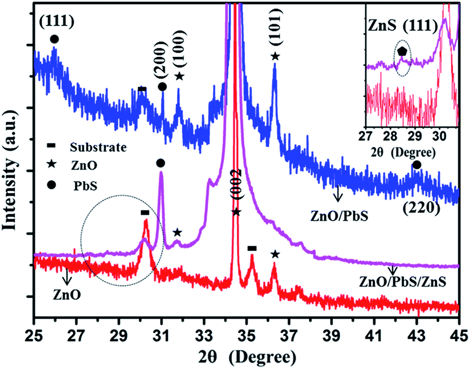 | ||
| Fig. 2 XRD spectra of ZnO nanorods, ZnO/PbS QDs and ZnO/PbS QDs/ZnS heterostructures. Inset is the enlarged spectra of the circle marked section. | ||
Based on above analysis, we can get the conclusion that both PbS shell and ZnS shell are formed by this in situ SILAR method. For their photodetection applications, the MSM photodetector based on these heterostructures are fabricated by forming indium electrodes on samples before and after SILAR procedures.19 The schematic diagram and spectral response spectra of the as-synthesized ZnO/PbS QDs heterostructure and ZnO/PbS QDs/ZnS heterostructure based broadband photodetectors under 15 V voltage are given in Fig. 3a. Both devices show response to visible light illumination. But different from the dual-band photodetector fabricated by Viraj Vishwakantha Jayaweera using ZnO and PbS,26 these two photodetectors show high responsivity over a wide range of wavelength extending from 340 nm to 840 nm instead of dual band spectral response corresponding to band gap of pure ZnO and PbS. Higher responsivity values are obtained for ZnO/PbS QDs/ZnS heterostructure based broadband photodetector, which indicates that further formation of ZnS shell contributes to the device performance improvements.
 | ||
| Fig. 3 (a) Spectral response of QDs-on-wide band gap heterostructure based photodetectors under 15 V. Insets are the SEM of the as-synthesized device and schematic diagram for the as-synthesized heterostructure. The parameters of the indium electrodes are about 10 μm wide and 40 μm long. (b) Voltage-dependent spectral response of ZnO/PbS QDs based photodetector. (c) and (d) I–V curves of ZnO/PbS QDs and ZnO/PbS QDs/ZnS heterostructures. (e) Light absorption of the as-synthesized samples. | ||
To better understand this issue, the voltage-dependent photo response spectrum of ZnO/PbS QDs/ZnS based photodetector is provided in Fig. 3b. This photodetector is not self-powered as no photoresponse is observed at 0 V voltage. It is obvious that similar device performance is obtained under negative and positive voltages. In detail, the responsivity of the as-synthesized device shows voltage-dependent characteristic: the responsivity of the as-synthesized device to 562 nm light illumination is 0.019 A W−1 under 5 V and increases to 0.03 A W−1 under 10 V. When the voltage further increases to 15 V, the responsivity reaches 0.04 A W−1. To further analyze the working mechanism of this ZnO/PbS QDs/ZnS based photodetector, I–V characterization is performed as shown in Fig. 3c. No obvious rectifying characteristic is observed, which is in good accordance with result in Fig. 3b. Considering the complex heterostructure interfaces, I–V characterization of ZnO/PbS QDs heterostructure is given in Fig. 3d. Both heterostructures show response to blue light illumination, but no obvious rectifying characteristic is observed, which indicates that no typical type II structure is formed between ZnO and PbS.19 This result is different from our previous report, which may be caused by the increasing size of QDs (average size in this report is 10 nm, which is two times compared to the size of QDs formed in our previous work). The size variation may arise from the decreasing solubility of Pb(NO3)2 and Na2S in methanol solution.19 To better understand the improvements of device performance caused by introduction of ZnS shell, their light absorption spectra are given in Fig. 3e. Similar to our previous work, obvious visible light absorption is achieved when PbS QDs layer is formed on the surface of ZnO owing to the formation of interface between ZnO and PbS.19 Light absorption in the whole range is further enhanced by deposition of ZnS shell, but not too much, which means that variations in light absorption did not contribute too much to the increased responsivity of ZnO/PbS QDs/ZnS heterostructure based photodetector. That is to say, some more key factors exist in determining the final device performance of this heterostructure based photodetector besides the production of charge carriers in the QD layers and the size related band gap modulation. This conclusion can be further confirmed by direct head-to-head comparison of photodetectors, performances by introducing heterostructures formed by using mixture solutions of water and ethanol as solvents of Pb(NO3)2 and Na2S solutions.
According to our previous report, visible light absorption is enhanced when PbS QDs are formed on ZnO by using the mixture of ethanol and water as solvents of Pb(NO3)2 solution and Na2S solution. Type-II structure is achieved between PbS and ZnO on the condition when ZnO is firstly immersed into Pb(NO3)2 solution.19 The formation of type-II structure is believed to facilitate separation of photo-induced carriers by prompting the electron flow from PbS to ZnO. Most importantly, the existences of ligands, such as NO3−, are excluded based on our previous XPS characterization results.27 But, different from theoretical assumption, no spectral response is observed on this case, which indicates that even though the absence of extra ligands is one of the greatest advantages of this in situ SILAR method, particular attention is still needed, especially on the following two aspects:
(1) Carrier separation and transport at the interface between ZnO and PbS QDs.
(2) Carrier transport within PbS QDs.
Introduction of organic materials by SILAR method can be excluded as illustrated by our previous work, but formation of complex interfaces or surfaces are inevitable for heterostructures. As it is well known, device performance in practical is mainly affected by their defects related interfaces and surfaces characteristics. Herein, defects related characterizations are performed by Raman and PL method as shown in Fig. 4a and b. In the Raman spectrum of ZnO sample, Raman-active phonon modes at 101 cm−1, 437 cm−1 and 574 cm−1 corresponding to its E2(low), E2(high) and A1(LO) are observed.28 The feature at 333 cm−1 is a second order Raman modes that occurs under resonance condition. A peak at around 181 cm−1 is observed for ZnO/PbS heterostructure indicating the formation of PbS QDs on ZnO.29 The oxidation of PbS can be eliminated as no obvious Raman peaks belong to the oxidation products at 966 cm−1 is observed.29 The formation of ZnS can be confirmed by the appearance of broad overtone peak at about 650 cm−1.30 Generally, Raman peaks above 380 cm−1 are observed in the Raman spectrum of ZnS, which are the combinations of acoustic and optical modes. For example, the peaks at 622 cm−1 and 676 cm−1 correspond to 2TO and 2LO overtones along the L-K-H and H-K lines, respectively. The sum of the TO and LO mode frequencies of phonons at H, M, and L points are close to 646 cm−1. It is noted that the intensity of E2(M) increases from ZnO sample to ZnO/PbS and ZnO/PbS/ZnS heterostructures, which suggests that the formation of PbS shell and ZnS shell have an effects on the local environment around the host atom and thus the lattice normal symmetry. Another thing that is noteworthy to mention that the intensity of ZnO A1(LO) peak at around 580 cm−1 for ZnO/PbS and ZnO/PbS/ZnS heterostructures is higher compared to pure ZnO. This can be understood as follows: A fairly higher density of interface states are expected to be present at the grain boundaries. The defects act as acceptors level which capture the charge carriers from the interior of heterostructures and enhance the formation of depletion barrier.31 The presence of depletion layer develops a strong build-in electric field at interface and surfaces. The scattering by Raman active optical phonos is enhanced by the formation of electric field due to polarization by the field of the excitonic states. That is to say, the intensity of the assigned A1(LO) mode is closely related with defects density. The higher intensity of A1(LO) mode in ZnO/PbS QDs heterostructure indicates that defects were formed during SILAR processes besides the passivation of dangling bonds at the surface of ZnO.32 Most importantly, more defects are introduced during further formation of ZnS shell for ZnS/PbS/ZnO heterostructure as much higher intensity of A1(LO) mode is obtained. This can be further confirmed by PL spectra characterization results shown in Fig. 4b. The characterization on the photoluminescence properties of ZnO, ZnO/PbS heterostructure and ZnS/PbS/ZnO heterostructure tend to provide information about defects in these nanostructures. One can see that all PL spectra show an obvious ultraviolet (UV) emission and a broad visible light emission. It is reported that the UV emission originates from the recombination of free excitons in the near-band-edge of the wide band gap ZnO and the broad visible luminescence has commonly been attributed to defects in ZnO. Forming shells on ZnO caused a large decrease in UV emission intensity. One possible reason for the decrease is that parts of luminescence are absorbed by PbS shell, which results in less luminescence can be detected. The other reason for the decrease shall be the existing of defects, which facilitate the separation of photo-induced excitons resulting in the decreasing recombinations of excitons. In fact, efficient charge separations make it suitable for photodetection applications. The defects-related green light at 575 nm and orange light emissions were obtained in pure ZnO nanorodes.33 Generally, the green and orange luminescence bands have been attributed to vacancies-related defects and interstitials-related defects, respectively. Especially, the light luminescence at 528 nm is zinc vacancies related light emission.34 When PbS shell is formed on ZnO, orange light emission and green light emission decreases indicating the formation of PbS shell by SILAR method passivates the dangling bonds at surfaces and some vacancies-related defects such as oxygen vacancies. Meanwhile, the presence of light emission at 528 nm indicates that formation of PbS QDs on the surface of ZnO also influence the chemical state of zinc atoms at surfaces. The light emission at 484 nm may be attributed to sulphate vacancies formed during the initial formation of PbS QDs on the surface of ZnO nanorods.35 For ZnS/PbS/ZnO heterostructure, visible light emissions at both 528 nm and 484 nm disappeared, which confirms that formation of ZnS shell can passivate some defects formed during the formation of PbS QDs on the surface of ZnO such as zinc vacancies and sulphate vacancies. At the same time, orange light illumination is enhanced compared to ZnO/PbS heterostructure, which indicates that the formation of ZnS shell introduces defects at the same time. This is in good accordance with the HRTEM and Raman result in Fig. 2i and 4a. It is also noteworthy to mention that the effects of shell on luminescence characteristics are in close relationship with the number of layers. Herein, no obvious peak shifts or light emission from ZnS shell are observed indicate the formation thin shell layer, which agrees well with the XRD result in Fig. 2.36 All these results are reasonable and can be understood by M. Sookhakians work. According to their report, more surface vacancies and nonradiative recombination sites are created or exposed unprotected during the early stage of shell formation.25
 | ||
| Fig. 4 Raman and PL spectra of ZnO nanorods, ZnO/PbS QDs heterostructure and ZnO/PbS QDs/ZnS heterostructure. | ||
According to Elisabeth Franziska Zillner,s report, initial charge separation, which is one of the most essential factors for the achievement of bandbroadening photodetection, is in close relationship with interface related defects characteristics of QDs at the first monolayer.37 Herein it should be QDs monolayer grown directly on the surface of ZnO nanorods. Together with the fact that QDs are formed on wide band gap semiconductor by liquid phase methods, it is reasonable to believe that the solution characteristics play essential roles in their final device performances. In the aqueous containing solution, S2− tends to hydrolysis forming HS−, H2S, which may destroy the interfaces between ZnO and PbS as both ZnO and PbS are sensitive to acid stuff. In detail, when H2S reacts to form the initial ZnS nucleis, Zn2+ slowly dissolves from the surface of ZnO and initial ZnS shell is then formed by ions exchange reaction between H2S and Zn2+. R. Yi et al. reported the existence of intermediate gap and diffusion bridge between core and shell, in which the dissolved zinc ions and oxygen ions can migrate.38 All these results well explained the fact that more defects are formed by this etching process, which may act as combination centers of photo-induced carriers and inhibit the efficient extraction of carriers at interfaces. This can be further confirmed by comparing the results with the case for heterostructure formed by using aqueous-containing solution as solvents. When aqueous-containing solvents are used as solvents, their XRD shows no PbS related peaks unless the sample is annealed at 150 °C due to the poor crystalline. PL spectrum of ZnO/PbS QDs shown in ESI† presents increasing visible light emission which indicates that more defects are formed.
It is noteworthy to point out that excess Zn related defects may be involved when ZnS shell is introduced, the improved device performance may thus be attributed to the passivation of dangling bonds at the surface of QDs, which illustrates the key role of surface passivation to their photodetection applications. Another factor deserves our attention is the distance between QDs also affects the carrier transport within QDs layer by influencing their electronic coupling characteristic between nanocrystals.39 Herein, densely distributed PbS QDs are formed on ZnO by SILAR method by dipping ZnO into Na2S solution firstly.19 Thus, it is understandable that ZnO/PbS QDs/ZnS based broadband photodetector can be achieved just by suitable solvent and dipping order choosing during SILAR method.
All these experiment results indicate that the interface and surface modulations play key roles in their photodetector applications besides the formation of type II heterostructures, which can be explained by mechanism exhibited in Fig. 5a–c:39 free charge carriers are created in PdS QDs by absorption of visible light. The excited charge carriers relax from excited states above the band edges into the lowest excitonic state. Under illumination, the dominant mechanism was a separation of photo-induced carriers. Some charge carriers photo-excited within QDs recombine radiatively or nonradiatively. Trapping of photo-excited carriers at interfaces took place. The remaining free holes are subsequently either trapped on PdS QD surfaces or diffuse into neighbouring QDs under certain voltage. Control over the interfaces related defect density thus improves the photodetectors, performance by providing a pathway with lower recombination centers. Surface trap states modulation by further introducing ZnS shell improve the device performance by increasing photocurrent within heterostructure as less carriers can be trapped by surface defects. Fig. 5d and e are the time response spectrum of the as-synthesized device. Obvious current increases to blue light (545 nm), green light (518 nm) and red light (632 nm) and ultraviolet light are observed. The slow increase under ultraviolet illumination can be attributed to the filling of defects existing within this heterostructure.
 | ||
| Fig. 5 Processes of charge separation within ZnO/PbS QDs/ZnS heterostructure. (a) Visible light absorption of PbS QDs. (b) Charge carrier recombination and trapping of photo induced carriers at ZnO/PbS QDs and PbS QDs/ZnS interfaces. (c) Trapping and diffusion of carriers within ZnO/PbS QDs/ZnS heterostructure under positive voltage. (d) and (e) Time response spectra of ZnO/PbS QDs/ZnS heterostructure based photodetector to different light illuminations. | ||
Conclusions
In summary, an in situ fabrication method is introduced for fabrication of PbS QDs-on-wide band gap semiconductor heterostructure which prompts the efficient carrier transport within QDs by avoiding the existence of additional ligands. Broadening band photodetection ranging from ultraviolet to visible light is feasibly achieved by this in situ fabrication method. Especially, improved device performance is achieved even in the case that no obvious type-II heterostructure is formed between ZnO and PbS, which remind us that defects control of QDs based devices deserves more concerns besides suitable size, shape and band gap modulations. All these explorations may thus provide different ideas on fabrication and improvement of QDs-on-wide semiconductor heterostructures based broadband photodetectors.Acknowledgements
This work is supported by the National Natural Science Foundation of China (Grant No. 61306014 and No. 61574051). Natural Science Foundation of Heilongjiang Province of China (E2015002), and Open Project Program of Key Laboratory for Photonic and Electric Bandgap Materials, Ministry of Education, Harbin Normal University (PEBM201406).References
- G. Cheng, X. Wu, B. Liu, B. Li, X. Zhang and Z. Du, Appl. Phys. Lett., 2011, 99, 203105 CrossRef.
- J. P. Clifford, G. Konstantatos, K. W. Johnston, S. Hoogland, L. Levina and E. H. Sargent, Nat. Nanotechnol., 2009, 4, 40–44 CrossRef CAS PubMed.
- F. Guo, B. Yang, Y. Yuan, Z. Xiao, Q. Dong, Y. Bi and J. A. Huang, Nat. Nanotechnol., 2012, 7, 798–802 CrossRef CAS PubMed.
- A. Sobhni, M. W. Knight, Y. Wang, B. Zheng, N. S. L. King, V. Brown, Z. Fang, P. Nordlander and N. J. Halas, Nat. Commun., 2012, 4, 1643 CrossRef PubMed.
- Z. Lou, L. Li and G. Shen, Nanoscale, 2016, 8, 5219–5225 RSC.
- H. Yuan, X. Liu, F. Afshinmanesh, W. Li, G. Xu, J. Sun, B. Lian, A. G. Curto, G. Ye, Y. Hikita, Z. Shen, S.-C. Zhang, X. Chen, M. Brongersma, H. Y. Hwang and Y. Cui, Nat. Nanotechnol., 2015, 10, 707–713 CrossRef CAS PubMed.
- M. Chen, L. Hu, J. Xu, M. Liao, L. Wu and X. Fang, Small, 2011, 7, 2449 CAS.
- L. Hu, M. Chen, W. Shan, T. Zhan, M. Liao, X. Fang, X. Hu and L. Wu, Adv. Mater., 2012, 24, 5872 CrossRef CAS PubMed.
- Q. E. Semonin, J. M. Luther, S. Choi, H.-Y. Chen, J. B. Gao, A. J. Nozik and M. C. Beard, Science, 2011, 334, 1530–1533 CrossRef PubMed.
- J. M. Luther, J. Gao, M. T. Lioyd, O. E. Semonin, M. C. Beard and A. J. Nozik, Adv. Mater., 2010, 22, 3704–3707 CrossRef CAS PubMed.
- Y.-H. Lee, B.-M. Huang and H.-T. Chien, Chem. Mater., 2008, 20, 6903–6905 CrossRef CAS.
- S.-Q. Fan, Q. Kim, J.-J. Kim, D. W. Jung, S. O. Kang and J. Ko, Electrochem. Commun., 2009, 11, 1337–1339 CrossRef CAS.
- B. N. Pal, I. Robel, A. Mohite, R. Laocharoensuk, D. J. Werder and V. I. Klimov, Adv. Funct. Mater., 2012, 22, 1741–1748 CrossRef CAS.
- D. Qi, M. Fischbein, M. Drndić and S. Šelmić, Appl. Phys. Lett., 2005, 86, 093103 CrossRef.
- G. Konstantatos, L. Levina, A. Fischer and E. H. Sargent, Nano Lett., 2008, 8, 1446–1450 CrossRef CAS PubMed.
- J. Tang, K. W. Kemp, S. Hoogland, K. S. Jeong, H. Liu, L. Levina, M. Furukawa, X. Wang, R. Debnath, D. Cha, K. W. Chou, A. Fischer, A. Amassian, J. B. Asbury and E. H. Sargent, Nat. Mater., 2011, 10, 765–771 CrossRef CAS PubMed.
- G. L. Koleilat, L. Levina, H. Shukla, S. H. Myrskog and S. Hinds, ACS Nano, 2008, 2, 833–840 CrossRef CAS PubMed.
- F. Dubois, B. Mahler, B. Dubertret, E. Doris and C. A Mioskowski, J. Am. Chem. Soc., 2007, 129, 482–483 CrossRef CAS PubMed.
- H. L. Li, S. J. Jiao, H. T. Li, L. Li and X. Zhang, CrystEngComm, 2015, 17, 4722–4728 RSC.
- S.-H. Jung, E. Oh, K.-H. Lee, W. Park and S.-H. Jeong, Adv. Mater., 2007, 19, 749–753 CrossRef CAS.
- C. Ratanatawanate, C. Xiong and K. J. Balkus Jr, ACS Nano, 2008, 2, 1682–1688 CrossRef CAS PubMed.
- X. Fan, M.-L. Zhang, I. Shafiq, W.-J. Zhang, C.-S. Lee and S.-T. Lee, Adv. Mater., 2009, 21, 2393–2396 CrossRef CAS.
- Z. Q. Zhang and J. Mu, J. Colloid Interface Sci., 2007, 307, 79 CrossRef CAS PubMed.
- Y. Z. Zhang, Y. P. Liu, L. H. Wu, H. Li, L. Z. Han, B. C. Wang and E. Xie, Appl. Surf. Sci., 2009, 255, 4801 CrossRef CAS.
- M. Sookhakian, Y. M. Amin, W. J. Basirun, M. T. Tajabadi and N. Kamarulzaman, J. Lumin., 2014, 145, 244 CrossRef CAS.
- P. V. V. Jayaweera, P. K. D. Duleepa, P. Pitigala, J. F. Shao, K. Tennakone, A. G. U. Perera and S. Member, IEEE Trans. Electron Devices, 2010, 57, 2756–2760 CrossRef CAS.
- H. L. Li, S. J. Jiao, J. X. Ren, H. T. Li, S. Y. Gao, J. Z. Wang, D. B. Wang, Q. J. Yu, Y. Zhang and L. Li, Phys. Chem. Chem. Phys., 2016, 18, 4144 RSC.
- X. Q. Wei, B. Y. Man, M. Liu, C. S. Xue, H. Z. Zhuang and C. Yang, Physica B, 2007, 388, 145–152 CrossRef CAS.
- G. D. Smith, S. Firth and R. J. H. Clark, J. Appl. Phys., 2002, 92, 4375–4380 CrossRef CAS.
- W. G. Nilsen, Phys. Rev., 1969, 182, 838–850 CrossRef CAS.
- C. Sudakar, P. Kharel, G. Lawes, R. Suryanarayanan, R. Naik and V. M. Naik, J. Phys.: Condens. Matter, 2007, 19, 026212 CrossRef.
- C. F. Windisch, G. J. Exarhos, C. Yao and L.-Q. Wang, J. Appl. Phys., 2007, 101, 123711 CrossRef.
- Y. Hu, H. Qian, Y. Liu, G. Du, F. Zhang, L. Wang and X. Hu, CrystEngComm, 2011, 13, 3438 RSC.
- O. M. Ntwaeaborwaa, R. E. Kroona, V. Kumara, T. Dubrocab, J.-P. Ahnc, J.-K. Parkc and H. C. Swarta, J. Phys. Chem. Solids, 2009, 70, 1438 CrossRef.
- M. Sookhakian, Y. M. Amin, W. J. Basirun, M. T. Tajabadi and N. Kamarulzaman, J. Lumin., 2014, 145, 244 CrossRef CAS.
- J. S. Steckel, J. P. Zimmer, S. Coe-Sullivan, N. E. Stott, V. Bulović and M. G. Bawendi, Angew. Chem., Int. Ed., 2004, 43, 2154 CrossRef CAS PubMed.
- E. F. Zillner, Ph.D. thesis, Institut for Heterogene Materialsysteme am Helmholtz-Zentrum Berlin für Materialien und Energie, German, 2013.
- R. Yi, G. Qiu and X. Liu, J. Solid State Chem., 2009, 182, 2791 CrossRef CAS.
- K. S. Jeong, J. Tang, H. Liu, J. Kim, A. W. Schaefer, K. Kemp, L. Levina, X. Wang, S. Hoogland, R. Debnath, L. Brzozowski, E. H. Sargent and J. B. Asbury, ACS Nano, 2012, 6, 89–99 CrossRef CAS PubMed.
Footnote |
| † Electronic supplementary information (ESI) available. See DOI: 10.1039/c6ra14574d |
| This journal is © The Royal Society of Chemistry 2016 |