
Review of neuromorphic computing based on NAND flash memory
Sung-Tae Lee *a and
Jong-Ho Lee*bc
*a and
Jong-Ho Lee*bc
aSchool of Electronic and Electrical Engineering, Hongik University, Seoul 04066, Republic of Korea. E-mail: lst777@hongik.ac.kr
bThe Inter-University Semiconductor Research Center, Department of Electrical and Computer Engineering, Seoul National University, Seoul 08826, Republic of Korea. E-mail: jhl@snu.ac.kr
cMinstry of Sciecne and ICT, Sejong, Korea
First published on 17th July 2024
Abstract
The proliferation of data has facilitated global accessibility, which demands escalating amounts of power for data storage and processing purposes. In recent years, there has been a rise in research in the field of neuromorphic electronics, which draws inspiration from biological neurons and synapses. These electronics possess the ability to perform in-memory computing, which helps alleviate the limitations imposed by the ‘von Neumann bottleneck’ that exists between the memory and processor in the traditional von Neumann architecture. By leveraging their multi-bit non-volatility, characteristics that mimic biology, and Kirchhoff's law, neuromorphic electronics offer a promising solution to reduce the power consumption in processing vector–matrix multiplication tasks. Among all the existing nonvolatile memory technologies, NAND flash memory is one of the most competitive integrated solutions for the storage of large volumes of data. This work provides a comprehensive overview of the recent developments in neuromorphic computing based on NAND flash memory. Neuromorphic architectures using NAND flash memory for off-chip learning are presented with various quantization levels of input and weight. Next, neuromorphic architectures for on-chip learning are presented using standard backpropagation and feedback alignment algorithms. The array architecture, operation scheme, and electrical characteristics of NAND flash memory are discussed with a focus on the use of NAND flash memory in various neural network structures. Furthermore, the discrepancy of array architecture between on-chip learning and off-chip learning is addressed. This review article provides a foundation for understanding the neuromorphic computing based on the NAND flash memory and methods to utilize it based on application requirements.
1. Introduction
Recently, artificial intelligence (AI) has demonstrated significant progress in a wide range of cognitive tasks, including but not limited to natural language processing, speech recognition, and image classification.1–8 Nevertheless, high-performance deep neural networks (DNNs) necessitate a substantial increase in neural network size and a significant number of parameters, hence requiring high-performance graphics processing units (GPUs), extensive memory storage, and substantial computational capabilities.9–12 Furthermore, the von Neumann bottleneck gives rise to significant energy and time consumption during vector–matrix multiplication (VMM) operations as a consequence of the substantial data transfer between the memory and processor.The utilization of synaptic device arrays in neuromorphic systems has been comprehensively studied as a potential solution to address the von Neumann bottleneck through in-memory computation.13–15 When an input voltage is imposed on a synaptic array, the resulting current is determined by the product of the conductance of the synaptic device and the input voltage. According to Kirchhoff's current law (KCL), these currents, stemming from numerous devices connected to a single source-line (SL), are aggregated. The summation of currents in each SL in the array occurs concurrently. Hence, a synaptic device array has the capability to execute VMM in parallel within a single time step, resulting in much improved efficiency compared to the traditional von Neumann architecture.16
Previous research has mainly employed resistive random-access memories (RRAMs)17–23 and phase change memory (PCM) as synaptic devices in the neuromorphic systems.24–30 However, it is necessary to conduct additional research on various aspects of RRAMs, including device variability, the integration of selectors for large-scale integration,31 stochastic programming, and reliability. Additionally, it should be noted that the presence of an IR drop in a metal wire has the potential to cause inaccuracies in the VMM operation using an RRAM device array.32 Furthermore, the limited on/off current ratio of RRAM devices introduces a potential source of inaccuracy in the cumulative summation of currents from several synaptic devices.33,34 In addition, PCM requires additional research to resolve the issue of resistance drift. Time-dependent resistance drift in amorphous chalcogenide material of PCM is one of the major reliability concerns, particularly affecting multi-level cell (MLC) operations.35,36
To address the aforementioned challenges, it is possible to employ technologically mature and commercially competitive Si-based devices, such as NOR flash memory37–42 and static random-access memory (SRAM),43–50 as synaptic devices. Nevertheless, there exists a constraint in terms of density for both NOR flash and SRAM technologies. This limitation arises from the fact that a single cell in NOR flash memory occupies a relatively large footprint, while a single SRAM cell is composed of several transistors. On the other hand, NAND flash memory offers high integration density by reducing the number of ground wires and bit-line (BL) contacts, hence increasing cell density.
State-of-the-art DNN algorithms exhibit remarkable performance; however, they necessitate a significant number of parameters and a huge network size. Therefore, NAND flash memory cells possess the capability to effectively handle extensive parameters, making them a promising candidate for synaptic devices. This utilization offers notable benefits in terms of cell density, as well as a substantial storage capacity per chip. NAND flash memory technology has been widely recognized as one of the most competitive solutions for handling large-scale data storage needs.51–58 Furthermore, it has been shown that NAND flash memory is a technologically mature and commercially competitive option.59–61 Recent studies have proposed neuromorphic architectures to utilize NAND flash memory as a synaptic device despite the cell string structure.62–69
The majority of the review articles on neuromorphic devices focus on emerging memristive devices for artificial neuron and synapse applications. This review paper offers a comprehensive overview of recent advancements in neuromorphic computing based on the NAND flash memory. It begins by presenting neuromorphic architectures that employ NAND flash memory for off-chip learning, exploring different quantization levels for input and weight data. It then presents neuromorphic architectures designed for on-chip learning, utilizing standard backpropagation and feedback alignment algorithms. The article discusses the array architecture, operational scheme, and electrical characteristics of the NAND flash memory, with particular emphasis on its utilization in various neural network structures. Additionally, it addresses the differences in array architectures between off-chip and on-chip learning. In summary, this review article establishes a solid foundation for comprehending neuromorphic computing based on the NAND flash memory and offers insights into its application in accordance with specific requirements.
2. Off-chip learning based on NAND flash memory
A. Binary neural networks
Binary neural networks (BNNs) offer significant reductions in computing overhead and memory usage by binarizing weights and inputs to either 1 or −1.70–78 Instead of employing high-precision floating-point multiplication and accumulation (MAC) operations, BNNs utilize exclusive NOR (XNOR) operations and bit-counting. Therefore, it can provide a promising solution to the realization of hardware neural networks.71,77 Furthermore, recent research has demonstrated that BNNs can achieve a satisfying classification accuracy on well-known image datasets, including the Modified National Institute of Standards and Technology (MNIST), Canadian Institute for Advanced Research (CIFAR-10), and ImageNet.75–77Lee et al. proposed a 2T2S (two transistors and two NAND cell strings) synaptic string structure for XNOR operation in BNNs.62 Fig. 1 presents a synaptic string structure called the 2T2S (two transistors and two NAND cell strings) configuration for XNOR operation. This design employs two NAND cell strings for a single synapse string, consisting of serially connected NAND cells, with two input transistors for which the two input voltages are applied to the gates. Each synapse, formed by two adjacent NAND cells from two cell strings, can represent a synaptic weight of +1 when the left NAND cell and the right NAND cell have low threshold voltage (Vth,low) and high threshold voltage (Vth,high), respectively. In contrast, a synaptic weight of −1 is defined as the opposite state of the two NAND cells. For input values, a value of +1 is defined using complementary input voltages, where Vin1 and Vin2 are the turn-on voltage (Von) and the turn-off voltage (Voff), respectively. In contrast, a value of −1 can be defined as the opposite pattern of the two input voltages. Through the aforementioned approach, the string current (ISL), denoting an XNOR output, is determined by the combination of the complementary input voltages and the state of the two neighboring NAND flash cells. Fig. 1(a) and (b) illustrate these cases for input values of +1 and −1, respectively.
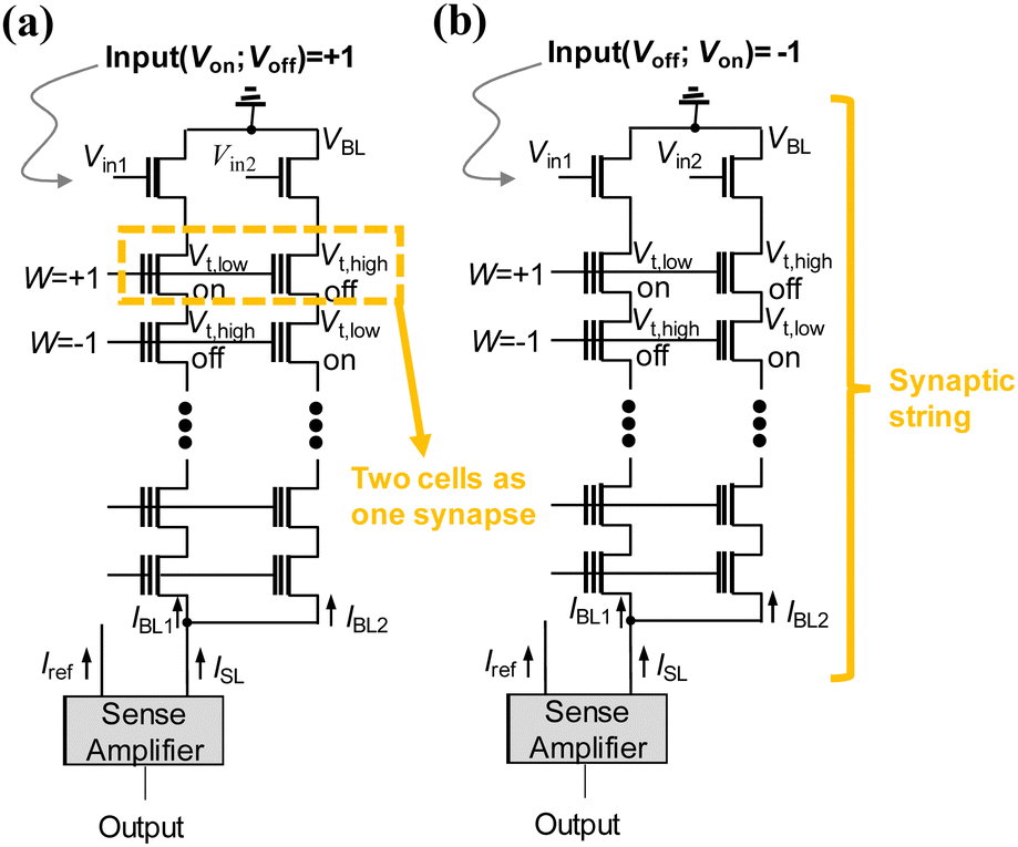 | ||
| Fig. 1 2T2S (two input transistors and two NAND strings) synaptic string structure with a sense amplifier using a fixed reference current (IREF). This figure has been reproduced from ref. 62 with permission from IEEE, copyright 2019. | ||
In the proposed scheme, the NAND cell in the Nth row of the synaptic string in Fig. 1(a) is connected to the Nth post-synaptic neuron. As the read bias (Vread) is sequentially applied to the word-lines (WLs) along the synapse string, the output for each post-synaptic neuron is generated sequentially. This approach allows us to reuse the current-sensing circuit (CSA) for all synapses in the cell string, decreasing circuit complexity and increasing integration density. Additionally, the 2T2S design operates solely in the digital domain, removing the need for bulky operational amplifiers or analog-to-digital converters (ADC) that are typically essential in the analog VMM.
Fig. 2(a) represents a current-latch based CSA circuit designed for BNNs. The circuit is subjected to simulation using an ISL (composed of two bit-line currents (IBLs)) measured in62 and a 20-nm FinFET based Berkeley short channel IGFET model – common multi-gate (BSIM-CMG) model.79 Under conditions where the Ion and Ioff of the NAND cell are 590 nA and 0.1 pA, respectively, Fig. 2(b) and (c) show transient waveforms for the XNOR output of +1 and −1, respectively. The CSA detects the Ion of the NAND cell, resulting in a read access time of 2 ns, when the XNOR output is +1. Conversely, the CSA senses the IREF, leading to an extended read access time of 12 ns, when the XNOR output is −1.
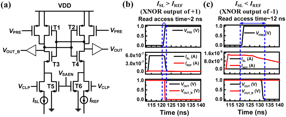 | ||
| Fig. 2 (a) The CSA which compares IREF with the string current ISL. Simulated transient results of CSA when XNOR output of (a) +1 (ISL > IREF) and (b) −1 (ISL < IREF). This figure has been reproduced from ref. 62 with permission from IEEE, copyright 2019. | ||
In pursuit of achieving a reduced bit-error rate, Lee et al. introduced a synaptic string structure known as 4T2S (four transistors and two NAND cell strings) for performing XNOR operations within BNNs.63 This 4T2S configuration incorporates a differential sensing scheme within the NAND string. Each synaptic string comprises two NAND strings and is constructed from synaptic cells connected in series, with four input transistors integrated into the design. These four input transistors receive Vin1 and Vin2 at their respective gates. It is noteworthy that these four input transistors are combined with a single sense amplifier, simplifying the synaptic string structure compared to the synaptic string and sense amplifier illustrated in Fig. 1.
Fig. 3(a) illustrates the synaptic string connected to a sense amplifier. Fig. 3(b) shows the differential current sense amplifier (DCSA), which includes two precharge PMOSFETs, four input transistors, and a cross-coupled inverter pair. Vin1 and Vin2 are applied to the gates of these input transistors. Importantly, these four input transistors are shared among all synapses within one synaptic string, effectively decreasing the number of input transistors compared to the scheme used in a prior study.77 This DCSA compares the two bit-line currents (IBL1, IBL2) of the two NAND flash cells to generate an XNOR output. Furthermore, the differential scheme eliminates the need for circuits to generate a fixed reference current source, which was required in the scheme depicted in Fig. 1. Additionally, it's possible to expand the functionality of the sense amplifier to contribute to logic operations, thereby reducing CMOS overhead. The DCSA reads the current of the NAND flash cells and simultaneously performs an XNOR operation.
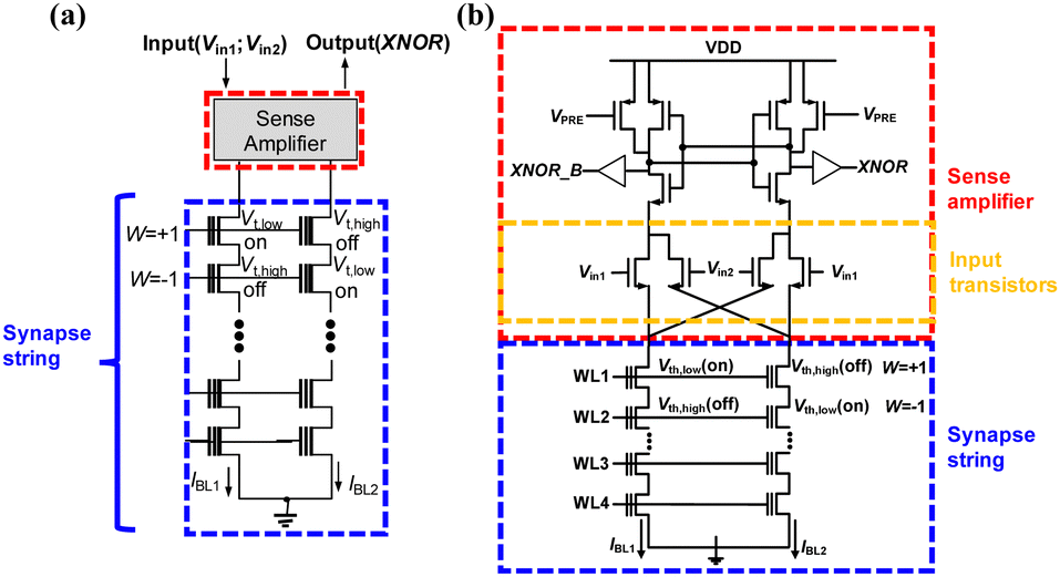 | ||
| Fig. 3 Differential sensing scheme utilizing 4T2S (four input transistors and two NAND strings) synaptic string structure with a sense amplifier. This figure has been reproduced from ref. 63 with permission from Elsevier, copyright 2022. | ||
Each synapse, composed of two neighboring NAND cells, employs the method depicted in Fig. 1 to represent synaptic weights. Concerning input values, a value of +1 is encoded using complementary input voltages, where Vin1 and Vin2 correspond to the Von and Voff, respectively. Conversely, to represent an input value of −1, the pattern of the two input voltages is inverted.
Fig. 4(a) represents the DCSA connected to a synapse string when the input is +1 (Vin1 = Von, Vin2 = Voff). Circuit simulations are conducted using a 20-nm FinFET-based BSIM-CMG model79 and the IBL of the NAND flash cells are measured.63 Fig. 4(b) and (c) represent transient waveforms for XNOR outputs of +1 and −1, respectively. Based on our measurements, the Ion and Ioff of the NAND cells are 480 nA and 1.4 pA, respectively. For a cell with a weight of +1, IBL1 is greater than IBL2 (IBL1 > IBL2), resulting in the DCSA generating an XNOR output of +1 with a read access time of approximately 1 ns. Conversely, for a cell with a weight of −1, IBL2 is greater than IBL1 (IBL2 > IBL1), and the DCSA generates an XNOR output of −1 with a similar read access time of about 1 ns. It's worth noting that the DCSA exhibits a faster sensing speed compared to the amplifier using a fixed reference current, as depicted in Fig. 4, when the XNOR output is −1. It is because the DCSA in the Fig. 4 senses the Ion while the CSA in the Fig. 2 senses the IREF when the XNOR output is −1.
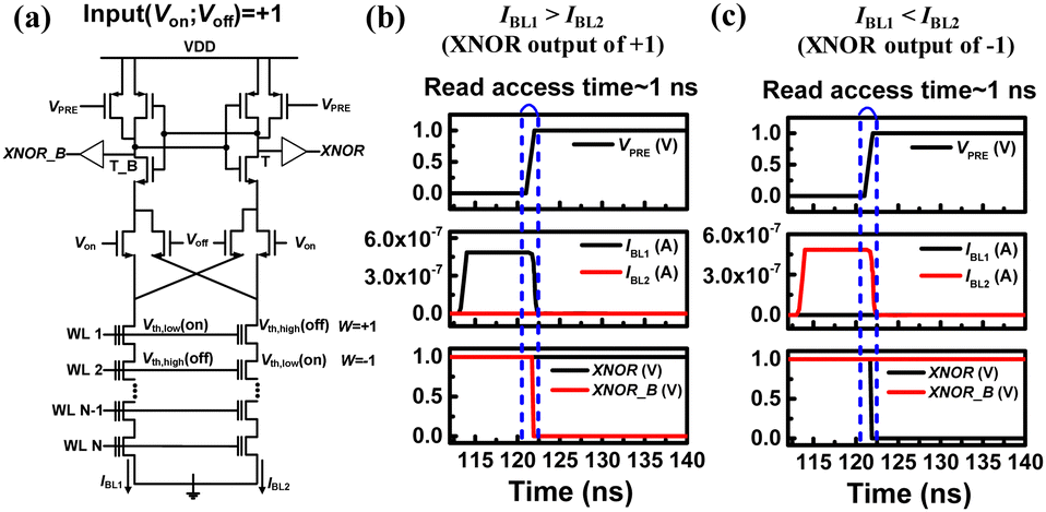 | ||
| Fig. 4 (a) The DCSA in the BNNs when the input is +1. Simulated transient results of the DCSA when (b) IBL1 > IBL2 and (c) IBL1 < IBL2. This figure has been reproduced from ref. 63 with permission from Elsevier, copyright 2022. | ||
Fig. 5 compares the inference accuracy versus bit error rate for the NAND flash memory synapses and reported RRAM synapses. As shown in this figure, NAND flash memory has a much lower bit error rate than RRAM devices in,73,78 because NAND flash memory has a higher on/off current ratio than RRAM devices. In addition, the differential sensing scheme of NAND flash memory can achieve a lower bit-error rate than the fixed reference current scheme of NAND flash memory due to its differential structure.
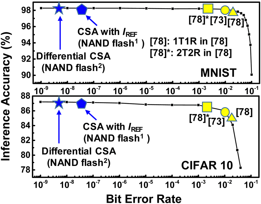 | ||
| Fig. 5 Inference accuracy for the MNIST and CIFAR 10 patterns with respect to bit error rates. This figure has been reproduced from ref. 63 with permission from Elsevier, copyright 2022. | ||
Fig. 6 represents the effective area per synapse and the synapse density ratio of the 2T2S structure and 2T2R (two transistors and two RRAMs) structure as the number of stacks increases. To calculate the area occupied by the 2T2R synapse, assumption has been made that two 22 nm FinFETs under two RRAMs determines the area of one synapse to be 24![[thin space (1/6-em)]](https://www.rsc.org/images/entities/char_2009.gif) 300 nm2. As the number of stacks grows, the effective area of a single synapse based on the VNAND flash memory diminishes. At a stack number of 128, the synapse density of VNAND is ∼100 times higher compared to that of the RRAMs.
300 nm2. As the number of stacks grows, the effective area of a single synapse based on the VNAND flash memory diminishes. At a stack number of 128, the synapse density of VNAND is ∼100 times higher compared to that of the RRAMs.
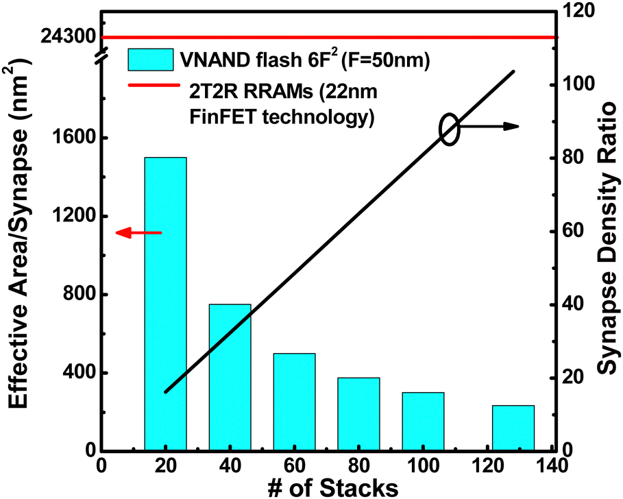 | ||
| Fig. 6 Effective area per synapse and synapse density ratio with the number of stacks. This figure has been reproduced from ref. 63 with permission from Elsevier, copyright 2022. | ||
B. Multi-bit quantized neural networks
Multi-bit quantized neural networks (QNN) can achieve higher inference accuracy than BNNs and comparable inference accuracy compared to neural networks having a floating-point weight. Wang et al. proposed 3-D vertical channel NAND array architecture to implement VMM operations.64Fig. 7 illustrates a biasing scheme designed for VMM operations on a 3-D NAND array, with the read operation being executed WL floor by WL floor. In the VMM operation, the same Vread is imposed on the SLs, while BLs are grounded. In the unselected WL floors, all WLs are biased at a higher pass bias (VPASS), ensuring that unselected transistors function as pass transistors, independently of their threshold voltage Vth values. The select voltage (VSEL) or ground is applied to the WLs in the selected floor based on the input vector pattern. Fig. 8 demonstrates the peripheral circuitry which applies the input vector and VPASS. Two sets of decoders are employed: one decoder supplies the VSEL to the WL of the selected floor, while the other decoder provides VPASS to the WLs in the unselected floors. The current in each pillar is primarily contingent upon the conductance of the NAND cell within the selected floor.
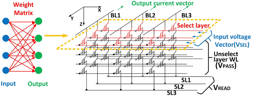 | ||
| Fig. 7 Circuit diagram and bias scheme of a 3-D vertical channel NAND array architecture for VMM. The weight in the neural networks is mapped to the conductance of the NAND cell in the selected WL floor. This figure has been reproduced from ref. 64 with permission from IEEE, copyright 2019. | ||
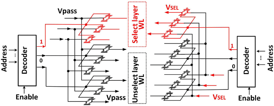 | ||
| Fig. 8 Peripheral circuitry control for applying the input vector to a selected floor and VPASS to the unselected floors. This figure has been reproduced from ref. 64 with permission from IEEE, copyright 2019. | ||
Subsequently, all drain currents are aggregated along the BLs to represent the weighted sum within the corresponding columns. The analog currents can be further sensed by analog-to-digital converters located at the end of the BLs. In essence, this VMM operation performed on a 3-D NAND array, when viewed from the top, bears resemblance to the same operation carried out on a 2-D NOR flash array. However, it's worth noting that at each cross point, there exists a series channel resistance from pass transistors in other unselected floors. This architecture can implement parallel VMM utilizing 3D NAND flash memory. However, WLs are separated in each floor, which is different from the existing NAND flash memory technology.
Lue et al. proposed neuromorphic architecture utilizing existing NAND flash memory without any modification, which can implement multi-bit weights and inputs utilizing multiple single-level cells and binary inputs.65 Fig. 9 depicts the methodology employed for the processing of VMM operations. In this process, we sequentially select a WL and accumulate the string current originating from multiple BLs to compile the accumulated current at the SL. Each block's SL is individually isolated and connected to its corresponding sense amplifier. It is noteworthy that in the context of 3D NAND, an additional terminal is introduced for the String Select Lines (SSLs). It is possible to simultaneously activate multiple SSLs to facilitate efficient 3D summation.
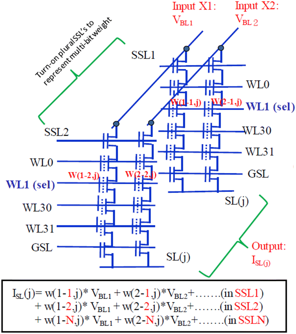 | ||
| Fig. 9 The operation method to emulate “VMM computing” using 3D NAND. String current is aggregated in the SL, where BLs serve as the inputs. Plural string-select lines (SSLs) represent multi-bit weight. Each block's SL amalgamates currents from many BLs and SSLs to produce the VMM output. This figure has been reproduced from ref. 65 with permission from IEEE, copyright 2019. | ||
The numerous BLs within the NAND architecture serve as input channels. We recommend employing single-level cell (SLC) storage for both weight and input, as it offers high reliability and simplifies the design without the need for complex digital-to-analog converters. On the other hand, the multiple SSLs provide a method for distributing the weight across multiple cells. For instance, a 3-SSL design can represent weight value of 0, 1, 2, 3 levels (2 bits) with binary storage for each cell. This approach can be expanded to various scenarios involving multi-bit representations. Unlike the prior research,64 which applied inputs to WLs and read outputs at BLs, this approach utilizes BLs as inputs and reads outputs at SLs. It can maximize the computing bandwidth.
They conducted measurements on a 16-floor 64Gb SLC single-gate vertical channel (SGVC) 3D NAND chip to gather the IBL distribution, depicted in Fig. 10(a). An extremely thin-body device with a channel thickness (Tsi) of approximately 3 nm, as illustrated in Fig. 10(b), is employed to inherently achieve lower mobility.80 This device can provide an ultra-low on-current (Ion) of ∼2 nA, while maintaining an excellent on/off current ratio and an exceptionally low off-current (Ioff). Such a low Ion and a substantial on/off current ratio offers significant bandwidth, enabling the parallel summation of over 10000 cells. This configuration greatly enhances the efficiency of DNN computing.
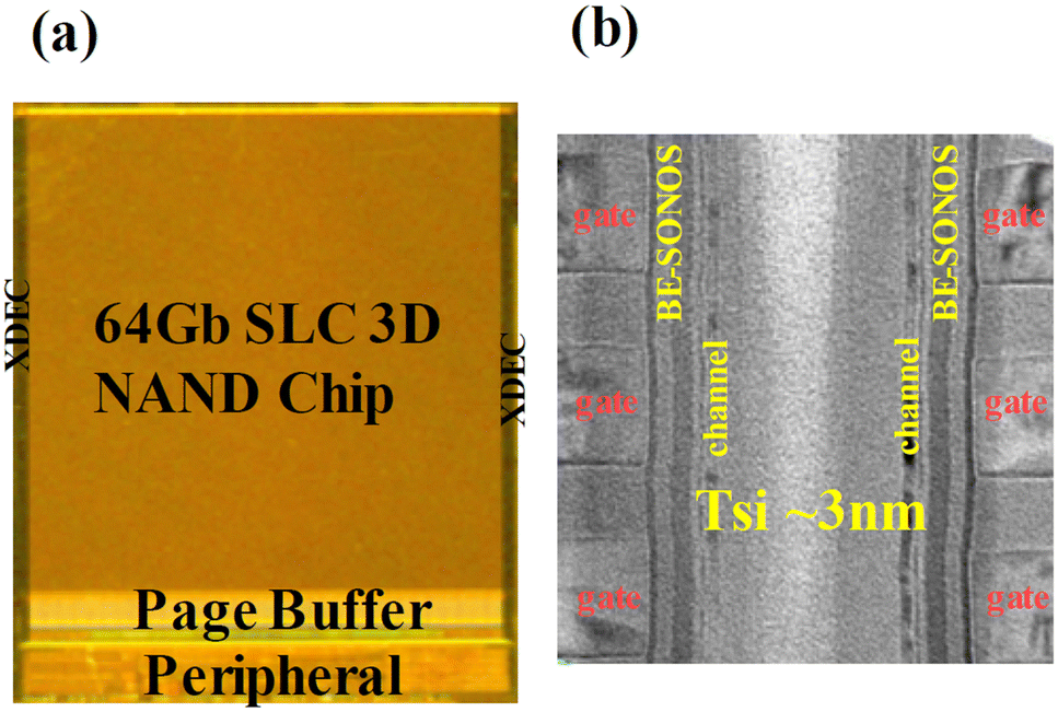 | ||
| Fig. 10 (a) A 64Gb SLC SGVC 3D NAND test chip for gathering string current distribution and noise data, essential for VMM computing. (b) An extremely thin-body 3D NAND device with a Tsi of ∼3 nm is employed to achieve an ultra-low Ion of ∼2 nA, while also ensuring a low Ioff of less than 1 pA. This figure has been reproduced from ref. 65 with permission from IEEE, copyright 2019. | ||
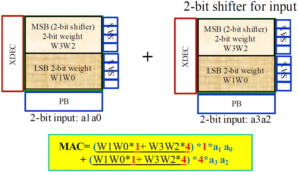
Fig. 11 presents an example for a 4-bit input and 4-bit weight configuration (4I4W), which is anticipated to become the standard in edge computing. Despite both weight and input being SLC operations, they employ a ‘shifter and adder’ design to achieve VMM with 4-bit inputs and 4-bit weights. In this design, the 3 SSLs correspond to 2-bit weight, and by introducing an additional block with a 2-bit shifter and adder, it creates 4-bit weight capability. On the input side, they utilize 3 BLs to represent 2-bit input, and similarly, by duplicating the tile with a 2-bit shifter, they implement 4-bit input. This approach can distribute each weight across 36 different cells, effectively representing 4I4W. The high-density 3D NAND technology enables extensive array replication without the need for complex analog memory design. The total number of BLs can exceed 10000, while still providing a reasonable sense amplifier working range with low background leakage. This extensive parallelism is highly efficient in accommodating modern neural network architectures, where the number of inputs often surpasses several thousand.
 | ||
| Fig. 11 Operation scheme for VMM of 4-bit inputs and 4-bit weights. This figure has been reproduced from ref. 65 with permission from IEEE, copyright 2019. | ||
Utilizing the measured IBL distribution, it can aggregate numerous cells in a random fashion to generate VMM outputs, depending on the various number of summations. What's remarkable is that the resulting VMM output current distribution, as illustrated in Fig. 12(a), exhibits an astonishing level of narrowness, despite the original wide IBL distribution.
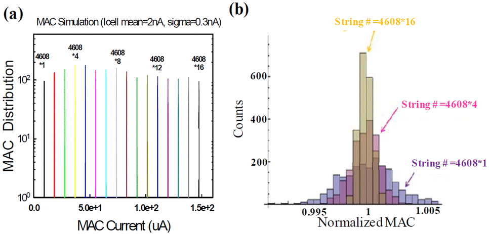 | ||
| Fig. 12 (a) Simulation of MAC currents, by assuming various summed numbers. The results reveal an impressively narrow VMM output distribution, capable of supporting resolutions exceeding 4 bits. (b) The normalized VMM current distribution, which becomes progressively narrow as the number of summations increases. This figure has been reproduced from ref. 65 with permission from IEEE, copyright 2019. | ||
As showcased in Fig. 12(b), this narrowness in the normalized VMM output current distribution becomes more pronounced as the number of strings involved in the summation process increases. Furthermore, Fig. 13 demonstrates a linear relationship between the normalized standard deviation of VMM output and the square root of N, where N represents the number of strings utilized for summation. This observation aligns seamlessly with the principles of the ‘Central Limit Theory,’ which posits that as the sample size grows, the mean of the summations tends to converge toward a normal distribution, and the normalized deviation diminishes (1/Sqrt(N)). This remarkable advantage can be attributed to the inherent high parallelism of 3D NAND nvCIM technology, which enables a substantial number of summations to be performed using multiple BLs and SSLs. Consequently, noise and variations are effectively averaged out, resulting in an exceptionally narrow VMM distribution centered around the mean value. This capability empowers precise VMM computations, even for operations involving higher resolution bit levels. However, in this method, multiple NAND cells should be used to represent a multi-bit weight and input.
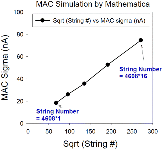 | ||
| Fig. 13 The standard deviation of VMM with sqrt (N), where N is the number of strings. ©2018 IEEE. Reprinted, with permission, from ref. 37. This figure has been reproduced from ref. 65 with permission from IEEE, copyright 2019. | ||
Bavandpour et al. proposed an ultra-compact and energy-efficient time-domain vector-by-matrix multiplier, leveraging the structure of commercial 3D-NAND flash memory, which utilizes two NAND cells to represent a multi-bit weight and input.66 The time-domain VMM approach, known for its superior area and energy efficiency compared to the current-mode VMM approach,81–84 is inherently compatible with the intricate 3D-NAND flash memory architecture without requiring any modifications. The innovative 3D-VMM adopts a resistive successive integration and re-scaling (RSIR) scheme, effectively eliminating the need for a bulky load capacitor that typically dominates the area- and energy-landscape in conventional time-domain VMMs.
The RSIR VMM is illustrated in Fig. 14 through its circuit schematic and timing diagram. Input bits are sequentially applied to the vector-by-matrix multiplier, with phase I involving P steps to achieve P-bit input precision. Each step consists of two operations: (a) integration and (b) re-scaling, controlled by non-overlapping signals ϕ2 and ϕ3. In the pth step, starting from the least significant bit (LSB), the pth bit of all inputs is selected using multiplexers and applied to the input lines. This action activates adjustable current sources with values proportional to the weights. At the end of the integration phase, the voltage across the resistor RI and capacitor CI is proportional to the weighted sum of the pth bits of input vector elements. During the re-scaling operation, CI detaches from RI and the weight current sources before connecting to an identical re-scaling capacitor CR (CR ≡ CI). The process of charge sharing between CI and CR achieves re-scaling of the intermediate results. Following P integration and re-scaling operations in phase I, the voltage on the CI and CR is proportional to the re-scaled version of the final dot product value. In phase II of the RSIR scheme, a similar process to the charge-based VMM scheme85 is employed for converting this voltage into a digital pulse. During this conversion, the integrate resistor is disconnected, and the capacitors are further charged using a sweeping current source. Once the voltage across the capacitor surpasses the threshold voltage (Vth) of the neuron, a digital pulse is generated at the output of the neuron circuitry. The duration of this pulse is proportional to the weighted summation of the input values.
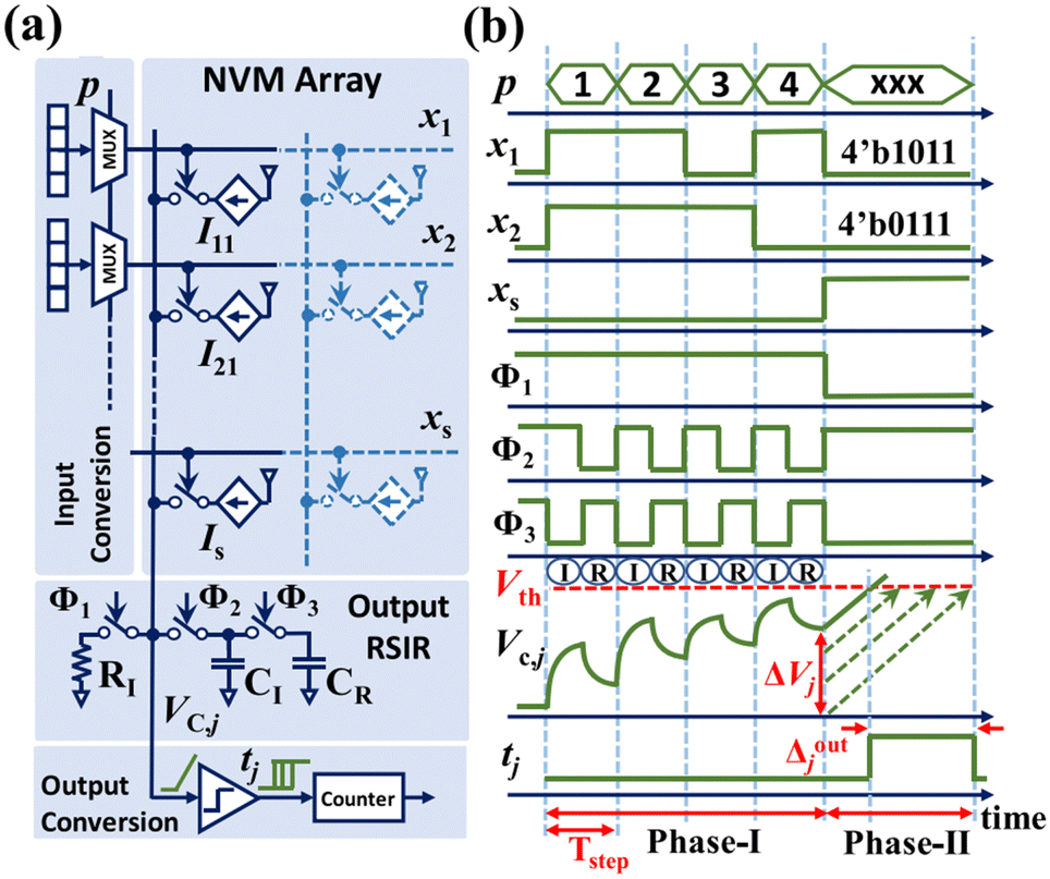 | ||
| Fig. 14 (a) Circuit diagram of the RSIR time-domain approach (b) timing diagram of RSIR operation scheme, assuming a 4-bit input conversion precision. For clarity, the figure illustrates the operation when memory cells are sourcing current. In the context of 3D-NAND memories, it's important to note that the memory cells typically act as sinks for the current. In such cases, the output circuitry connects to the bit-line side of the memory cell string. The output is initially pre-charged to a specific voltage, and subsequently discharged during RSIR operation. This figure has been reproduced from ref. 66 with permission from IOP Publishing, copyright 2021. | ||
A significant benefit of this resistive load-based scheme lies in its ability to discharge the charges injected into the integrated capacitor due to parasitic capacitive coupling from input strings over the transient period. Consequently, any disturbance charges during switching transients are effectively mitigated, exerting no influence on the voltage on the integrate capacitor. This relieves the stringent requirement for large output capacitors to sustain inference accuracy in time-domain VMM designs based on the 3D-NAND flash memory. Consequently, in the proposed RSIR scheme, the values of the output capacitors (CR and CI) are not reliant on the parasitic capacitance components of the 3D-NAND string. Instead, they are determined solely by the coupling capacitors of the pass-transistor-based switches, which are considerably smaller. Moreover, a smaller load capacitor necessitates a lower sweeping current during phase II of VMM operation. This reduced sweeping current can be supplied by configuring cells within specific rows of the same WL floor to reach the maximum string current value, enabling them by applying a high input solely to their SSL during phase II of computation. This option is unavailable in the charge-based approach, where the top floor memory cells must be selected to provide the relatively substantial sweeping currents. Consequently, the energy and delay overhead associated with switching the WL floors for phase II of VMM operation to generate the sweeping current is also eliminated when employing the RSIR approach. Another advantage of the RSIR approach is its suitability for VMM operations with sub-maximal output ranges, crucial for minimizing quantization errors. Indeed, the value of RI is determined by the range of the string current and the desired voltage swing on the drain (ΔVD). Therefore, VMMs with smaller output ranges can be implemented simply by increasing the value of RI.
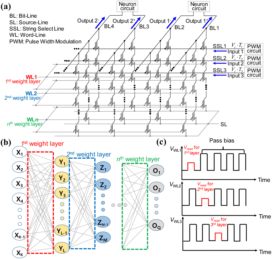
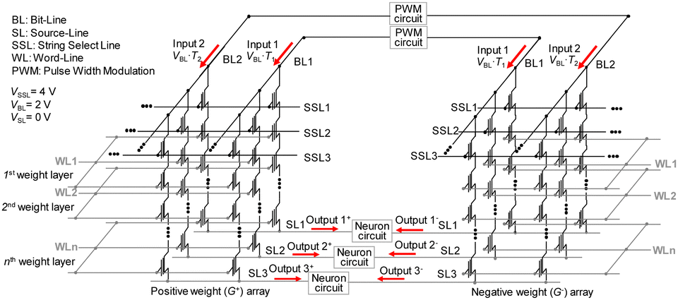
Lee et al. proposed an operation scheme for high-density and highly robust neuromorphic computing based on NAND flash memory architecture with analog inputs and 4-bit weights.67 Fig. 15 provides a schematic representation of the operational method of a neuromorphic system utilizing three-dimensional NAND flash memory with PWM circuits. The PWM circuits generate input voltages with adjustable pulse-width that are applied to the SSLs, where cell currents are aggregated in the BLs, as depicted in Fig. 15(a). The NAND cells within the kth WL correspond to the synapses in the kth synaptic layer of the neural network in Fig. 15(b). The operational method involves the application of a Vread and a VPASS to a selected WL and unselected WLs, respectively, as shown in Fig. 15(c). By sequentially imposing Vread on the WLs along the synaptic string, the output of each post-synaptic neuron is generated in sequence. Cells connected to selected WL store weights, with each weight determining the string current of its respective cell string. It is important to note that the proposed operation scheme diverges from that of the conventional NAND flash memory architecture. In the proposed scheme, the input bias corresponding to neuron activation is applied to SSLs, and the current summation takes place through the BLs. On the other hand, in the conventional NAND flash memory, the cell selected by the input address is read through the BL. Furthermore, in the proposed scheme, SSLs are concurrently biased by input voltage, whereas in the conventional NAND flash memory, read bias is sequentially applied to each SSL. As a result, this scheme significantly reduces latency compared to conventional NAND flash memory technology. In both schemes, the output current is read through the BL. Additionally, the proposed synaptic architecture utilizing NAND flash differs from the RRAM crossbar array. In the RRAM crossbar array, the input bias is applied to WLs, and the output current is aggregated through BLs. In the NAND cell array, cell strings consist of multiple cells connected in series. Within the NAND cell array, the WL and SL are shared by NAND strings within the same block of NAND flash memory. Moreover, to activate unselected cells, a VPASS must be applied to the WLs of those unselected cells. Consequently, in the proposed synaptic architecture, input is applied to SSLs, and the output current is read from the BLs. Furthermore, the cells in the kth floor within NAND flash strings represent the synapses in the kth synapse layer of neural networks. It is worth noting that the proposed operational scheme can be applied to both 2D and 3D NAND flash memory architectures.
 | ||
| Fig. 15 (a) Operation scheme for synaptic string array utilizing NAND flash memory with pulse width modulation (PWM) circuits. (b) Schematic diagram of neural networks. (c) Pulse timing diagram imposed on the WLs. This figure has been reproduced from ref. 67 with permission from Frontiers, copyright 2020. | ||
Fig. 16 illustrates the VMM operation utilizing a string array and neuron circuits within the neuromorphic system. In this system, the neuromorphic system represents weight and input of the DNN algorithm using the conductance and input voltage of synaptic devices, respectively. In the DNN algorithm, the weighted sum output exhibits a linear relationship with the input, as expressed by eqn (1),
 | (1) |
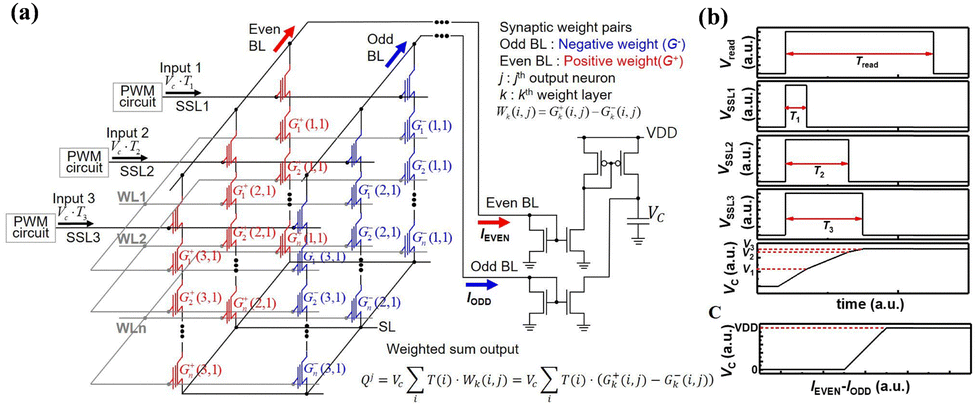 | ||
| Fig. 16 (a) Schematic representation of a synaptic string array, comprising synapses with positive weight (G+) and synapses with negative weight (G−). (b) Timing diagram illustrating the operational sequence and the voltage profile of the capacitor over time. (c) Behavior of the capacitor voltage (VC) in relation to the difference between IEVEN and IODD. This figure has been reproduced from ref. 67 with permission from Frontiers, copyright 2020. | ||
In neuromorphic systems, it is typically assumed that synaptic devices exhibit linear current versus voltage characteristics.86 When synaptic devices possess linear I–V characteristics, the input's amplitude within a DNN model can be straightforwardly represented by the input voltage amplitude of the synaptic devices. Consequently, the weighted sum current is represented as the product of the input voltage and the conductance of the synaptic devices, as indicated by eqn (2),
 | (2) |
However, NAND flash memory cell devices exhibit non-linear I–V characteristics, signifying that the output current exhibits a non-linear relationship with the input voltage. Consequently, it is challenging to represent the input's amplitude in a DNN algorithm using amplitude of input pulses. To address this issue stemming from the non-linear I–V characteristic of NAND cells, the PWM scheme is introduced. In this scheme, the input pulse's amplitude remains fixed, while the pulse width of the input pulse varies in proportion to the input's amplitude of a DNN algorithm. Subsequently, the weighted sum output is represented by the accumulated charge in neuron circuits, with the input voltage being applied, as shown in eqn (3),
 | (3) |
Hence, despite the non-linear I–V characteristics of the cell devices, the PWM scheme can implement the accurate execution of the weighted sum of DNN models within the neuromorphic systems. Furthermore, this scheme seamlessly aligns with the conventional NAND flash memory architecture. To represent negative weight values, two adjacent NAND cells are employed for one synaptic device. When considering negative weights, the charge accumulated in the neuron circuit can be represented using eqn (4),
 | (4) |
To implement current summing across time scales and subtraction between positive and negative weights, a configuration involving two current mirrors and one capacitor is adopted, as depicted in Fig. 16(a).87 In Fig. 16(a), synaptic devices connected to even BL and odd BL carry G+ and G−, respectively. The variables k, j, and i in the weighted sum equation in Fig. 16(a) correspond to the kth synapse layer, the jth post-synaptic neuron, and the ith synapse connected to the jth neuron, respectively.
Fig. 16(b) provides a visual representation of the pulse diagram of the operational scheme and the VC as an example for positive weight. During read time (Tread), Vread is applied to the selected WL, while VSSL1, VSSL2, and VSSL3 are applied to SSL1, SSL2, and SSL3 during T1, T2, and T3, respectively. Consequently, I1, I2, and I3 flow through NAND strings 1, 2, and 3, respectively. VC increases to V3, calculated as (I1·T1 + I2·T2 + I2·T2)/C. For simplicity, it is assumed that the weights of cells receiving read bias are identical. The voltage of VC is constrained by VDD and ground, establishing a relationship between VC and the difference between IEVEN and IODD, representing a hard-sigmoid function, one of the activation functions, as depicted in Fig. 16(c). In a specific current range where the difference between IEVEN and IODD falls within −(C·VDD)/(2·Tread) to (C·VDD)/(2·Tread), VC linearly increases with the difference between IEVEN and IODD. To simplify the description, it is assumed that IEVEN and IODD remain constant during Tread. Consequently, this scheme is capable of processing VMM operations involving 4-bit weights and analog input pulses, implementing neuron activation in a single input step without the need for additional logic operations. The PWM circuits, current mirrors, and capacitors are reused across all synapse layers (equivalent to WLs) in a synaptic string, significantly reducing the peripheral circuit area. It is worth noting that the convolution operation and VMM in multilayer neural networks are fundamentally the same operations when a 2D convolution kernel is unrolled into a 1D column.88 Consequently, the proposed scheme outlined in this work can be applied to the implementation of Convolutional Neural Networks (CNNs).
Fig. 17 depicts the curves illustrating IBL in relation to VBL with various weight levels. These measurements were conducted at a VPASS of 6 V and a VWL of 0 V. Each individual cell offers eight weight levels, corresponding to eight current levels ranging from 0 to 1.4 μA, with a consistent 200 nA difference between adjacent current levels. Notably, a synaptic device comprises both positive and negative weight cells, resulting in a 4-bit weight representation.
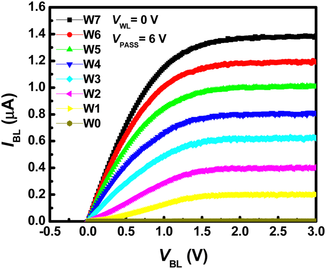 | ||
| Fig. 17 Characteristics of IBL versus BL voltage (VBL) with different weight levels at VPASS of 6 V and WL voltage (VWL) of 0 V. This figure has been reproduced from ref. 67 with permission from Frontiers, copyright 2020. | ||
Within the neuromorphic system, challenges arise due to the IR drop in metal wires, leading to inaccuracies in VMM operations, as the resistance in the metal wire diminishes the effective voltage applied to synaptic devices. Additionally, the channel resistance of neighboring cells, where pass bias is applied, can also introduce inaccuracies in VMM operations within NAND flash memory. To mitigate these issues, NAND cells are operated in the saturation region, mitigating concerns associated with wire resistance and pass cells in the unselected floors. In the saturation region, IBL exhibits minimal variation in response to changes in VBL, as illustrated in Fig. 17. Moreover, the minimum output resistance of a NAND cell operating in the saturation region is approximately 20 MΩ.
To investigate the impact of weight and input precision on the classification accuracy of neural networks, a QNN with 4-bit weight and analog input is compared to BNN with 1-bit weight and 1-bit input. Fig. 18 illustrates the inference accuracy of both QNN and BNN for CIFAR-10, employing CNN consisting of three fully connected layers and six convolution layers. It is noteworthy that, as the bit-width of weight and input decreases in QNN, the classification accuracy also decreases.89 This decline in accuracy is attributed to the quantization of weights and inputs, leading to weighted sum errors decreased classification accuracy. The final classification accuracies are 89.38% for QNN and 87.1% for BNN, respectively. Consequently, the proposed operational scheme enables the implementation of QNN with superior inference accuracy compared to BNN.
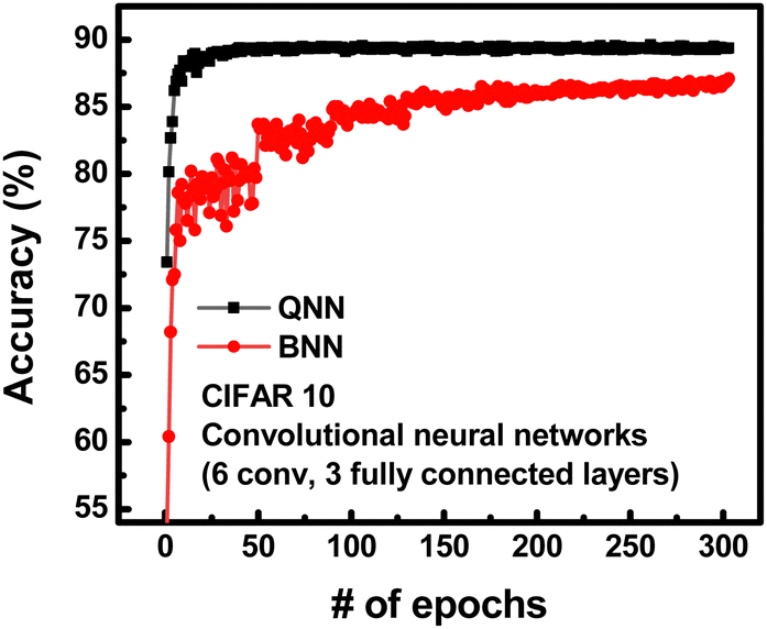 | ||
| Fig. 18 Simulation results depicting the classification accuracy comparison between QNN and BNN for CIFAR-10 images. This figure has been reproduced from ref. 67 with permission from Frontiers, copyright 2020. | ||
3. On-chip learning based on NAND flash memory
A. Utilizing transposed weights in backward propagation
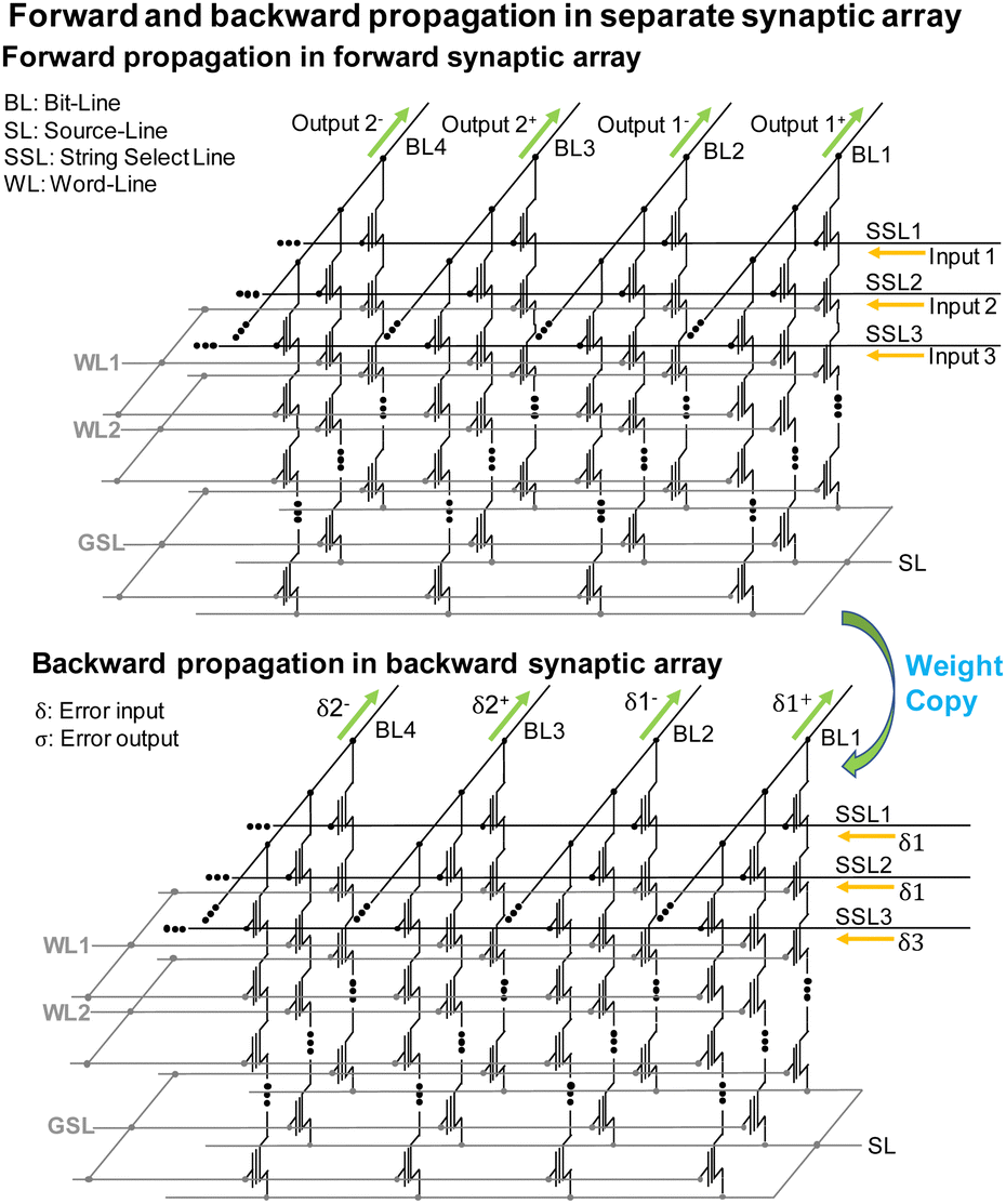
On-chip learning has the potential to considerably reduce both time and energy consumption during the training process compared to the off-chip learning. Moreover, it offers the advantage of compensating for weight variations in synaptic devices and adapting to changing real-time environments.90 In the case of RRAM crossbar arrays, on-chip learning can be easily implemented by applying inputs to rows during the forward pass and error inputs to columns during the backward pass.91 However, this approach cannot be employed when using NAND flash cells as synaptic devices for on-chip learning due to their cell string structure. Lee et al. proposed a novel method for enabling both forward propagation (FP) and backward propagation (BP) within the NAND flash memory array, facilitating on-chip learning.68Fig. 19 illustrates a synaptic device array in which two neighboring cells represent the G+ and G− of a single synapse within the synaptic array. FP can be correctly executed in the synaptic array, as depicted in Fig. 19. However, as shown in Fig. 19, it is not possible to conduct BP in a single time step within the synaptic array. To achieve BP in the synaptic array, error input1 (δ1) is initially applied, followed by error input2 (δ2).
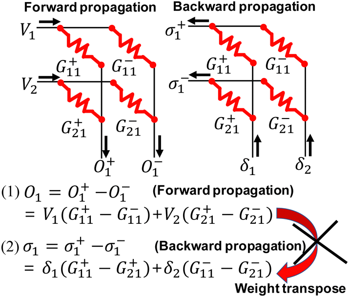 | ||
| Fig. 19 Architecture of a synaptic array comprising two adjacent cells, denoting G+ and G−. This figure has been reproduced from ref. 68 with permission from IEEE, copyright 2021. | ||
On the other hand, Fig. 20 presents a synaptic array where two cells representing G+ and G− of one synapse are segregated into distinct synaptic arrays. In this configuration, BP can be executed in a single time step, as demonstrated in Fig. 20. Consequently, separating G+ and G− is necessary to minimize latency during BP and successfully implement BP.
 | ||
| Fig. 20 Architecture of a synaptic array in which G+ and G− weights are segregated into distinct arrays. This figure has been reproduced from ref. 68 with permission from IEEE, copyright 2021. | ||
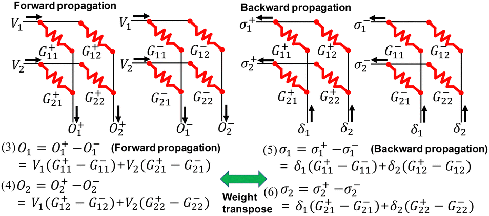
Fig. 21 and 22 illustrate the proposed circuit operation for performing FP and BP in the proposed synaptic architecture based on NAND flash memory, respectively, to enable on-chip learning. In conventional NAND flash memory, SLs are connected within a block, which hinders BP. To overcome this limitation, the synaptic architecture designed for operating both FP and BP in the same synaptic array separates SLs in a direction perpendicular to the BLs. Two NAND cells located in different synaptic weight arrays (G+ array, G− array) are utilized as one synapse to represent negative weight.
 | ||
| Fig. 21 Synaptic array architecture utilizing NAND flash memory for FP operation in on-chip learning. This figure has been reproduced from ref. 68 with permission from IEEE, copyright 2021. | ||
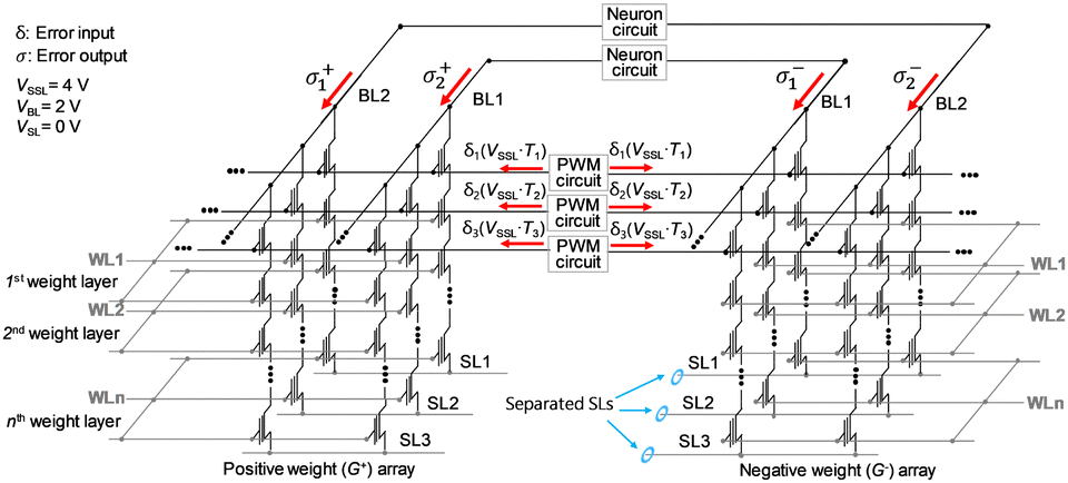 | ||
| Fig. 22 Synaptic array architecture employing NAND flash memory for BP operation in on-chip learning. This figure has been reproduced from ref. 68 with permission from IEEE, copyright 2021. | ||
During FP, input biases are applied to the BLs, and each weighted sum current is read from a separated SL. In BP, error inputs (δ) are applied to the SSLs, and each weighted sum current (σ) is read from a BL. If error inputs are applied to SLs and weighed sum current is read from BLs, which is the method used in RRAM array,91 the current of the cell at a WL location can be different in FP and BP due to the resistance of the pass cells, depending on the cell's location in the string.
To ensure consistency of the string currents between FP and BP, error inputs must be applied to SSLs, and the amplitudes of VSL, VSSL, and VBL should be the same in both FP and BP. The utilization of the same input voltage amplitude is achieved by using PWM circuits to generate width-modulated pulses with a fixed amplitude for both input and error input.92 By applying these width-modulated pulses to the VBL and VSSL during FP and BP, respectively, accurate VMM can be performed in both propagation stages, eliminating the impact of pass cells in the NAND flash memory architecture.
Notably, the IBL during FP and BP flow in the same direction. In this scheme, VSSL is applied to all SSLs to accumulate currents from NAND strings through BL. In contrast, conventional NAND flash memory operation applies VSSL to a selected SSL to read information from a NAND cell. Consequently, the proposed operation scheme can enhance throughput compared to the conventional NAND flash memory.
Fig. 23 presents a schematic of a neural network composed of n weight layers along with a pulse diagram over time. The cells connected to the kth WL of NAND flash memory in Fig. 21 and 22 represent synapses in the kth weight layer in Fig. 23(a). The Vread and VPASS are applied to a selected WL and unselected WLs, respectively, as shown in Fig. 23(b) and (c). Applying Vread to the kth WL produces the output of all neurons in the kth neuron layer. In FP, Vread is applied from the first to the nth WL to produce the weighted sum output. Conversely, during BP, Vread is applied from the nth to the first WL to produce the summed error. This scheme enables the transposition of synaptic weights and correct execution of both FP and BP in NAND flash memory.
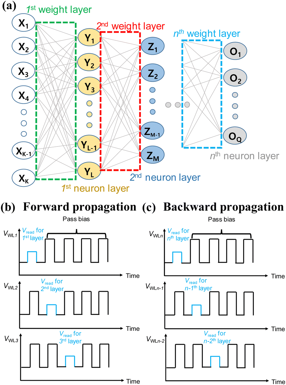 | ||
| Fig. 23 (a) Diagram illustrating neural networks comprising n weight layers. Timing diagram of VWL in the (b) FP and (c) BP. This figure has been reproduced from ref. 68 with permission from IEEE, copyright 2021. | ||
B. Utilizing random synaptic weights in backward propagation
In a system utilizing transposed weights in backward propagation presented above, an architectural design was introduced for on-chip learning that leveraged the structure of NAND flash memory.68 Nonetheless, the synaptic architecture described in68 differs from the conventional NAND flash memory structure in that it incorporates distinct SLs. Lee et al. proposed to employ a separate synaptic string array for implementing error backpropagation utilizing the conventional NAND flash memory, while incorporating random synaptic feedback weights.69To enable error backpropagation in the conventional NAND flash memory, it is essential to process forward and backward propagations in separate synaptic string array. Fig. 24 illustrates a case where both forward and backward propagations occur within the same synaptic devices of the NAND string array. In this architecture, forward propagation involves applying input voltages to the SSLs and reading the weighted sum currents through the BLs. For the backward propagation phase, the synaptic weights in the backward pass should be the transposed counterparts of those used in the forward pass. To achieve this weight transposition during backward propagation, error inputs need to be applied to the BLs, and the summed current should be read through the SSLs. However, it's important to note that the weighted sum current cannot flow through the SSLs. Consequently, it is not feasible to execute both forward and backward propagations within the same synaptic devices of the NAND flash memory.
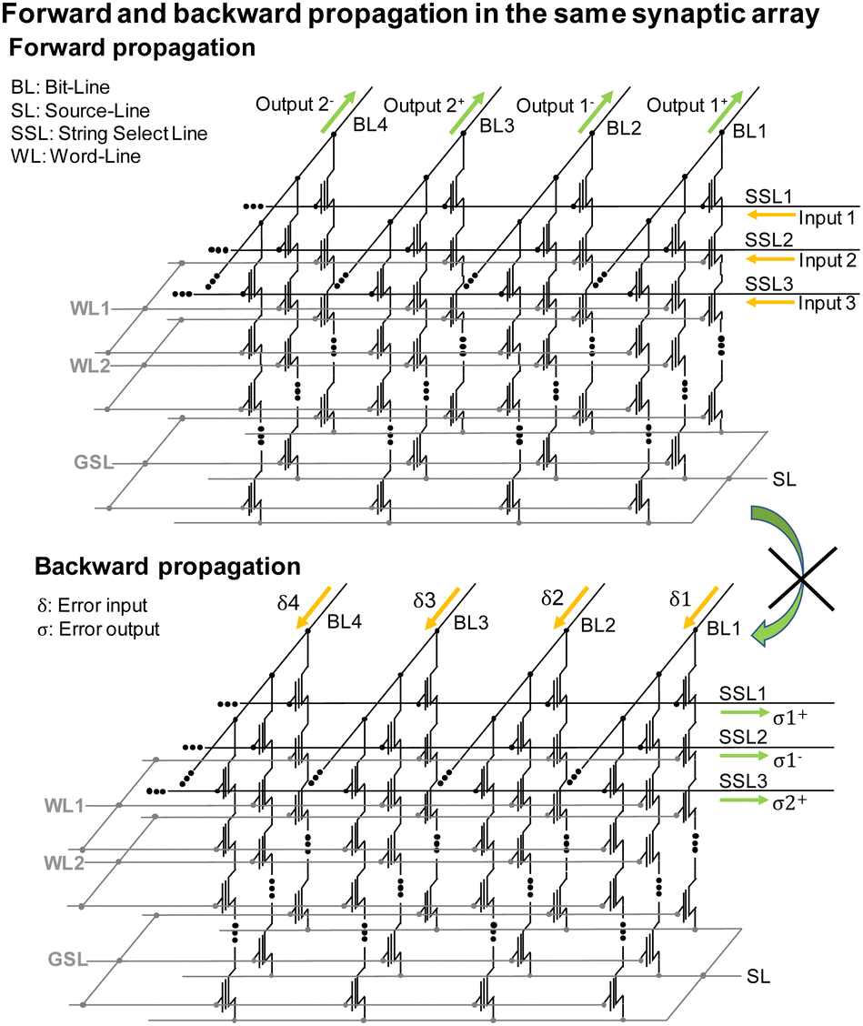 | ||
| Fig. 24 Operation scheme of synaptic string array where both forward and backward propagations are processed in the same array. This figure has been reproduced from ref. 69 with permission from IEEE, copyright 2023. | ||
Fig. 25 depicts a configuration where forward and backward propagations are conducted in separate synaptic arrays of the NAND flash memory. Forward propagation involves applying input voltages to the SSLs and summing the output currents through the BLs within the forward synaptic array. For backward propagation, error inputs are applied to the SSLs, and error output currents are read through the BLs in the backward synaptic array, which is distinct from the forward synaptic array. However, it's essential to reiterate that the synaptic weights in the backward synaptic array should be the transposed forms of those in the forward synaptic array. As a result, fitting the synaptic weights in the backward synaptic array to the transposed forms for each iteration requires methods like incremental step pulse programming (ISPP)93 or read–verify–write (RVW) schemes,94 which consume significant time and energy resources.
 | ||
| Fig. 25 Operation scheme of synaptic string array where both forward and backward propagations are processed in the separate array. This figure has been reproduced from ref. 69 with permission from IEEE, copyright 2023. | ||
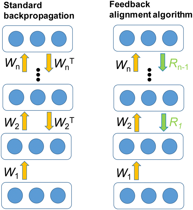
To address these challenges, while considering energy and time efficiency, we propose the application of the feedback alignment algorithm.95,96 This algorithm utilizes random synaptic feedback weights to facilitate error backpropagation within the conventional NAND flash-based synaptic array.
Fig. 26 illustrates a comparison between the standard backpropagation algorithm and the feedback alignment algorithm. In the standard backpropagation, the transposed weight (WT) is employed for the backward propagation phase. In contrast, the feedback alignment algorithm utilizes fixed random weights (R) for the backward propagation, rather than transposed weights (WT). During the training process, WT undergoes updates in each iteration, while R remains unchanged and fixed throughout each iteration.
 | ||
| Fig. 26 Comparison of standard backpropagation and feedback alignment algorithm. This figure has been reproduced from ref. 69 with permission from IEEE, copyright 2023. | ||
Fig. 27 shows the operational method of the conventional NAND flash memory-based synaptic architecture employing the feedback alignment algorithm. Forward propagation is accomplished by applying input voltages to the SSLs and summing the currents through the BLs in a forward synaptic array, which incorporates forward synaptic weights (W). For backward propagation, error inputs are applied to the SSLs, and the error outputs are summed through the BLs in a separate backward synaptic array that utilizes fixed random synaptic weights (R). It's important to note that the synaptic architecture using the random synaptic weight scheme necessitates an area twice as large as that using the standard backward algorithm, as it requires two separate NAND flash memory arrays for forward and backward propagations.
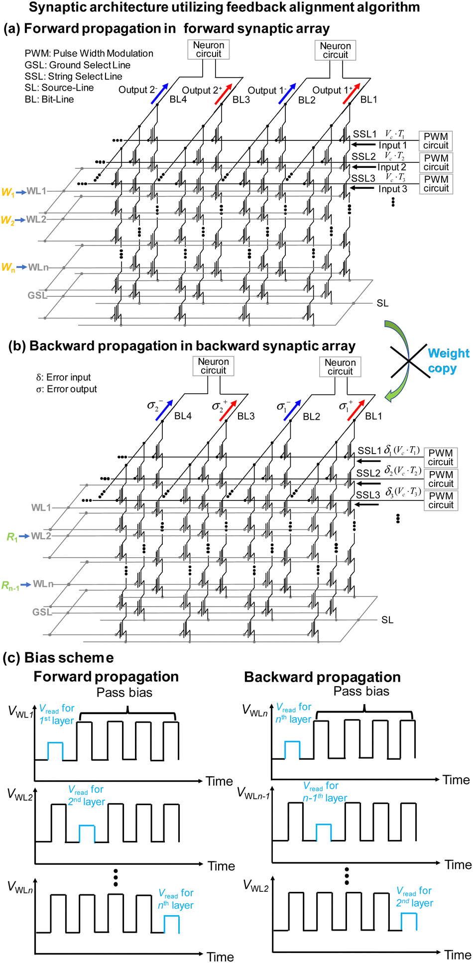 | ||
| Fig. 27 Operation scheme of synaptic string array where both (a) forward and (b) backward propagations are processed in the separate array utilizing random feedback synaptic weights. (c) Bias scheme of the VWL. This figure has been reproduced from ref. 69 with permission from IEEE, copyright 2023. | ||
However, the fixed random synaptic weights (R) in the backward synaptic array do not require weight updates, eliminating the need for methods like ISPP or RVW, which are typically needed to set the weights in backward propagation to the transposed forms of those in forward propagation. ISPP or RVW involves complex circuits that consume a significant amount of power to calculate the number of pulses required to accurately update the weights to their target values. Additionally, ISPP or RVW methods necessitate a substantial number of pulses to set the current of synaptic devices within the target current range.97 In contrast, the proposed scheme employing random synaptic weights requires only one program pulse of 14 V in each iteration. Consequently, the proposed method utilizing random synaptic weights significantly reduces both time and energy consumption.
By considering the sign of the weight update, only the weights of the forward synaptic array (W) are updated, while the weights of the backward synaptic array (R) remain fixed with a random distribution. An adaptive learning rule98 is employed to update the weight (W) of the forward synaptic array by one program pulse in each iteration, based on the sign of the weight update, thereby reducing the burden on the peripheral circuit.
The synaptic weights in the nth weight layer (Wn) of the forward pass in Fig. 26 are stored in the cells connected to the nth WL floor of the forward synaptic array in Fig. 27. When n weight layers are utilized in the forward pass, n − 1 weight layers are required in the backward pass, as depicted in Fig. 26. The synaptic weights in the n − 1th weight layer (Rn−1) of the backward pass in Fig. 26 are stored in the cells connected to the nth WL floor of the backward synaptic array in Fig. 27.
Fig. 27(c) represents the bias scheme of the synaptic string array. During forward propagation, Vreads are sequentially applied from the first WL to the nth WL floor of the forward synaptic array. In contrast, during backward propagation, Vreads are sequentially applied from the nth WL to the second WL floor of the backward synaptic array. This operational scheme enables the reuse of neuron circuits for every weight layer, reducing the burden on CMOS circuits compared to previous studies.62 Additionally, the proposed method can perform vector–matrix multiplication in a single pulse, eliminating the need for a multiplier and significantly reducing energy consumption.
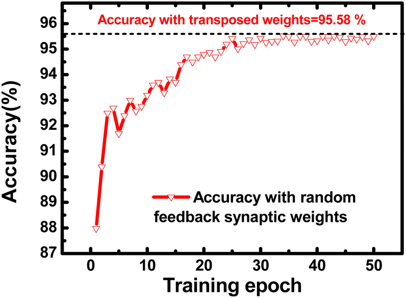
A simulation of a hardware-based fully connected neural network with a structure of 784-200-10 is conducted. Fig. 28 depicts the accuracy of the hardware-based neural networks as the training epochs increase. This network utilizes random synaptic feedback weights. After 50 epochs, the neural network with random synaptic feedback weights achieves an inference accuracy of 95.41%, which is similar to the inference accuracy of 95.58% obtained with the transposed weights. In these hardware-based neural networks, the Ion of synaptic devices is below 1 μA, and the Ioff of synaptic devices is below 1 pA. Additionally, VBL is set to 2 V, and the tread is 100 μs. The average energy consumed by a synaptic device to process one MNIST image is 4.1 × 10⁻¹⁵ J.
 | ||
| Fig. 28 Inference accuracy of hardware-based neural networks utilizing random feedback synaptic weights. This figure has been reproduced from ref. 69 with permission from IEEE, copyright 2023. | ||
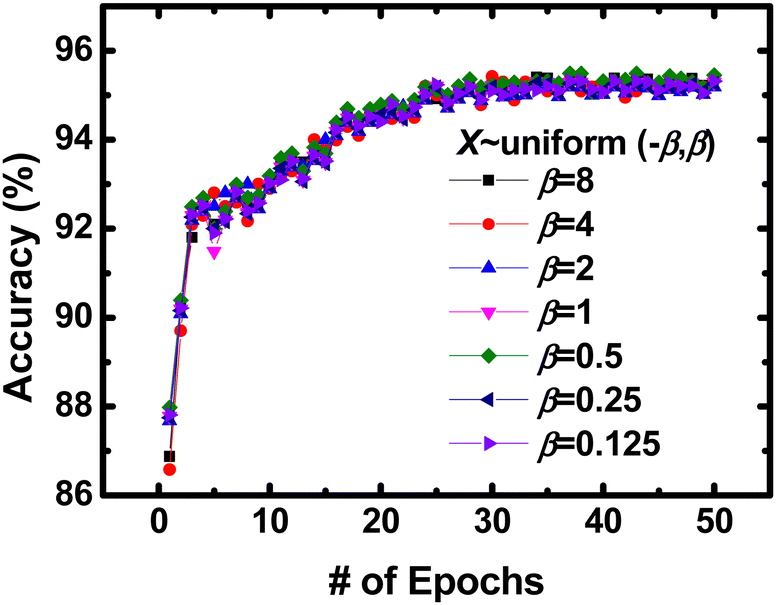
In a previous study on random synaptic weights,95 the initial values of the forward and backward weight arrays in random synaptic feedback were selected from a uniform distribution over the range of [−β, β], with the scale parameter (β) determined through manual search. They found that various scale parameters (β) for the uniform distribution performed well empirically. To determine the optimal scale parameters (β) for the hardware-based neural networks, a manual search is conducted. Values of β ranging from 0.125 to 8 worked effectively and achieved similar high inference accuracy as shown in Fig. 29. There was no significant difference or discernible trend in inference accuracies associated with different α values.
 | ||
| Fig. 29 Inference accuracy of hardware-based neural networks with various scale parameters β. This figure has been reproduced from ref. 69 with permission from IEEE, copyright 2023. | ||
4. Discussion
In this work, we reviewed recent works of synaptic devices based on the NAND flash memory. Firstly, the 2T2S synaptic string structure and sensing scheme for XNOR operation in BNNs is introduced.62 It can perform XNOR operation successfully for BNNs. However, it has an extended read access time of 12 ns, when the XNOR output is −1 due to the sensing scheme and requires reference current source. To achieve a lower read access time, and a lower bit-error rate, Lee et al. introduced a synaptic string structure known as 4T2S utilizing differential sensing scheme for performing XNOR operations within BNNs.63 The differential sensing scheme of63 exhibits a faster sensing speed compared to the sensing scheme of62 using a fixed reference current, when the XNOR output is −1. It is because the differential sensing scheme of63 senses the Ion while the sensing scheme of62 senses the IREF when the XNOR output is −1. In addition, the differential sensing scheme of63 can achieve a lower bit-error rate than the sensing scheme of62 due to its differential structure. Furthermore, 4T2S structure of63 simplifies the synaptic string structure compared to the 2T2S structure and sense amplifier of62 and can eliminate the need of reference current source. However, these structures for XNOR operations in BNNs have lower inference accuracy than multi-bit neural networks.Multi-bit quantized neural networks (QNN) can achieve higher inference accuracy than BNNs and comparable inference accuracy compared to the neural networks having floating-point weight. A 3-D vertical channel NAND array architecture to implement multi-bit VMM operations is introduced.64 It can implement parallel multi-bit VMM operations in NAND flash memory. However, the NAND flash memory proposed in64 separates WLs in each floor, which is different from the existing NAND flash memory technology. The separated WLs increase RC delay and IR drop, leading to the increased latency and inaccuracies in VMM operations. To utilize existing NAND flash memory without any modification, Lue et al. proposed neuromorphic architecture which can implement multi-bit weights and inputs utilizing multiple single-level cells and binary inputs.65 The numerous BLs within the NAND architecture serve as input channels, and the multiple SSLs provide a method for distributing the weight across multiple cells. Thanks to the principles of the 'Central Limit Theory’, noise and variations are effectively averaged out, resulting in an exceptionally narrow VMM distribution centered around the mean value. This capability empowers precise VMM computations, even for operations involving higher resolution bit levels. However, in this method, multiple NAND cells should be used to represent a multi-bit weight and input. To utilize two NAND cells to represent a multi-bit weight and input, Bavandpour et al. proposed an ultra-compact and energy-efficient time-domain vector-by-matrix multiplier, leveraging the structure of commercial 3D-NAND flash memory.66 The innovative 3D-VMM adopts a RSIR scheme, effectively eliminating the need for a bulky load capacitor that typically dominates the area- and energy-landscape in conventional time-domain VMMs. However, this architecture needs the digital clock to represent multi-bit input. To implement analog input, Lee et al. proposed an operation scheme for high-density and highly robust neuromorphic computing based on the NAND flash memory architecture with analog inputs and 4-bit weights.67 This architecture can represent analog input values by generating input voltages with adjustable pulse-width that are applied to the SSLs. In addition, this architecture is operated in the saturation region, which can reduce the IR drop in metal wires and channel resistance of the pass cells. However, the proposed architectures introduced for off-chip learning consume large amounts of power during training process and cannot adapt to the changing environment.
On-chip learning has the potential to considerably reduce both time and energy consumption during the training process compared to the off-chip learning. Moreover, it offers the advantage of compensating for weight variations in synaptic devices and adapting to changing real-time environments. To implement on-chip learning, Lee et al. proposed a novel method for enabling both FP and BP within the NAND flash memory array.68 The synaptic architecture separates SLs in a direction perpendicular to the BLs, which can operate both FP and BP in the same synaptic array. However, the separated SLs increase RC delay and IR drop, leading to the increased latency and inaccuracies in VMM operations. To utilize the structure of existing NAND flash memory for on-chip learning, Lee et al. proposed to employ a separate synaptic string array for implementing error backpropagation, while incorporating random synaptic feedback weights.69 The synaptic architecture using the random synaptic weight scheme necessitates an area twice as large as that using the standard backward algorithm, as it requires two separate NAND flash memory arrays for forward and backward propagations. However, this architecture can implement both forward and backward propagations in the existing NAND flash memory structure. In addition, the fixed random synaptic weights (R) in the backward synaptic array do not require weight updates, eliminating the need for methods like ISPP or RVW, which are typically needed to set the weights in backward propagation to the transposed forms of those in forward propagation. Consequently, the proposed method utilizing random synaptic weights significantly reduces both time and energy consumption.
The overall comparison of the synaptic architectures based on the NAND flash memory is represented in Table 1.
| Ref. | Learning type | Input terminal | Output terminal | Operation voltage | Pass bias | On-current (IBL) | The number of WL floors | Input, Weight resolution | Characteristics |
|---|---|---|---|---|---|---|---|---|---|
| 62 and 63 | Off-chip learning | Gate of input transistor | Bit-line | 0.4 V | 6 V | 600 nA | 64 | Binary weight, binary input | 1. Propose 2T2S structure to perform XNOR operation62 |
| 2. Propose 4T2S structure to perform XNOR operation63 | |||||||||
| 3. 4T2S reduces a bit-error rate and a read access time compared to the 2T2S. | |||||||||
| 64 | Off-chip learning | Word-line | Bit-line | 0.5 V | 8 V | 100 nA | 64 | Multi-bit weight, binary input | 1. Utilizing separate WLs to apply inputs to the WLs |
| 65 | Off-chip learning | Bit-line | Source-line | 0.2 V | 4.5 V | 2 nA | 16 | Multi-bit weight, multi-bit input | 1. Utilizing multiple binary cells to represent multi-bit weighted sum |
| 2. Extremely-thin body of 3 nm | |||||||||
| 3. Ultra-low on current of 2 nA | |||||||||
| 66 | Off-chip learning | String-select line | Bit-line | 0.7 V | — | 100 nA | 64 | Multi-bit weight, multi-bit input | 1. Utilizing successive integrate and re-scaling (RSIR) approach to represent multi-bit input |
| 2. Eliminating the need for a bulky load capacitor | |||||||||
| 67 | Off-chip learning | String-select line | Bit-line | 2 V | 6 V | <1.4 μA | 64 | Multi-bit weight, Multi-bit input | 1. Utilizing pulse width modulation method to represent multi-bit input |
| 2. Operating NAND cells in saturation region | |||||||||
| 68 | On-chip learning | Forward: bit-line backward: string-select line | Forward: source-line backward: bit-line | 2 V | 6 V | 200 nA | 64 | Multi-bit weight, Multi-bit input | 1. Implementing forward and backward propagations in the same NAND flash memory |
| 2. Utilizing the same single VPGM | |||||||||
| 69 | On-chip learning | String-select line | Bit-line | 2 V | 6 V | 200 nA | 64 | Multi-bit weight, multi-bit input | 1. Implementing forward and backward propagations in the separate NAND flash memory |
| 2. Utilizing random synaptic weights |
5. Conclusions
In this work, we reviewed recent works of synaptic devices based on the NAND flash memory. Firstly, synaptic architectures based on the NAND flash memory for off-chip learning were reviewed. The 2T2S structure can implement XNOR operation for binary neural networks utilizing the cell string structure. In addition, the 4T2S structure utilizes a differential sensing scheme which can reduce the bit-error rate compared to the 2T2S structure. To increase inference accuracy, the architecture using multi-bit weights and inputs was introduced. Various synaptic architectures utilizing multiple cells for one synapse, RSIR scheme, and PWM scheme were reviewed. Next, synaptic architectures for on-chip learning were introduced to mitigate the effects of device variations. The operation scheme utilizing transposed weights was introduced which can implement forward and backward propagations in the NAND flash memory with separated SLs. Then, the synaptic architecture utilizing random feedback synaptic weights was introduced to process forward and backward propagations in the conventional NAND flash memory.Conflicts of interest
There are no conflicts to declare.Acknowledgements
This research was supported by the National R&D Program through the National Research Foundation of Korea (NRF) funded by the Ministry of Science and ICT (MSIT) (RS-2023-00258527, RS-2022-00166543), the Technology Innovation Program (RS-2022-00154905) funded by the Ministry of Trade, Industry & Energy (MOTIE, Korea), and the 2023 Hongik University Research Fund.References
- A. Amberkar, P. Awasarmol, G. Deshmukh and P. Dave, International Conference on Current Trends towards Converging Technologies (ICCTCT), Coimbatore, India, 2018.
- Z. Leini and S. Xiaolei, J. Phys.: Conf. Ser., 2021, 1754, 1 CrossRef.
- D. Guiming, W. Xia, W. Guangyan, Z. Yan and L. Dan, 2016 IEEE International Conference on Signal and Image Processing (ICSIP), Beijing, China, 2016.
- M. Goyal, T. Knackstedt, S. Yan and S. Hassanpour, Comput. Biol. Med., 2020, 127, 104065 CrossRef PubMed.
- B. Jena, S. Saxena, G. K. Nayak, L. Saba, N. Sharma and J. S. Suri, Comput. Biol. Med., 2021, 137, 104803 CrossRef PubMed.
- A. A. Elngar, M. Arafa, A. Fathy, B. Moustafa, O. Mahmoud, M. Shaban and N. Fawzy, J. Cybersec. Inform. Manage., 2021, 6, 18–50 Search PubMed.
- Z. Xiong, Y. Yuan and Q. Wang, IGARSS 2018 – 2018 IEEE International Geoscience and Remote Sensing Symposium, Valencia, Spain, 2018.
- P. Aggarwal, N. K. Mishra, B. Fatimah, P. Singh, A. Gupta and S. D. Joshi, Comput. Biol. Med., 2022, 144, 105350 CrossRef CAS PubMed.
- M. M. Najafabadi, F. Villanustre, T. M. Khoshgoftaar, N. Seliya, R. Wald and E. Muharemagic, J. Big Data, 2015, 2, 1–21 CrossRef.
- O. Y. Al-Jarrah, P. D. Yoo, S. Muhaidat, G. K. Karagiannidis and K. Taha, Big Data Res., 2015, 2(3), 87–93 CrossRef.
- S. Gupta, A. Agrawal, K. Gopalakrishnan and P. Narayanan, International Conference on Machine Learning, June, 2015.
- M. Gheisari, G. Wang and M. Z. A. Bhuiyan, 2017 IEEE International Conference on Computational Science and Engineering (CSE) and IEEE International Conference on Embedded and Ubiquitous Computing (EUC), July, 2017.
- N. K. Upadhyay, H. Jiang, Z. Wang, S. Asapu, Q. Xia and J. Yang, Adv. Mater. Technol., 2019, 4(4), 1800589 CrossRef.
- G. Indiveri and S. C. Liu, Proc. IEEE, 2015, 103(8), 1379–1397 CAS.
- D. S. Jeong and C. S. Hwang, Adv. Mater., 2018, 30(42), 1704729 CrossRef PubMed.
- M. Hu, R. S. Williams, J. P. Strachan, Z. Li, E. M. Grafals, N. Davila, C. Graves, S. Lam, N. Ge and J. J. Yang, Proc. 53rd Annu. Des. Autom. Conf., 2016.
- V. Milo, C. Zambelli, P. Olivo, E. Pérez, M. K. Mahadevaiah, O. G. Ossorio, C. Wenger and D. Ielmini, APL Mater., 2019, 7(8), 081120 CrossRef.
- D. Panda, C. A. Chu, A. Pradhan, S. Chandrasekharan, B. Pattanayak, S. M. Sze and T. Y. Tseng, Semicond. Sci. Technol., 2021, 36(4), 045002 CrossRef CAS.
- E. Covi, S. Brivio, J. Frascaroli, M. Fanciulli and S. Spiga, ECS Trans., 2017, 75(32), 85 CrossRef CAS.
- J. Woo, A. Padovani, K. Moon, M. Kwak, L. Larcher and H. Hwang, IEEE Electron Device Lett., 2017, 38(9), 1220–1223 CAS.
- A. Padovani, J. Woo, H. Hwang and L. Larcher, IEEE Electron Device Lett., 2018, 39(5), 672–675 Search PubMed.
- J. Woo, K. Moon, J. Song, S. Lee, M. Kwak, J. Park and H. Hwang, IEEE Electron Device Lett., 2016, 37(8), 994–997 CAS.
- X. Hong, D. J. Loy, P. A. Dananjaya, F. Tan, C. Ng and W. Lew, J. Mater. Sci., 2018, 53, 8720–8746 CrossRef CAS.
- F. Jiao, B. Chen, K. Ding, K. Li, L. Wang, X. Zeng and F. Rao, Appl. Mater. Today, 2020, 20, 100641 CrossRef.
- L. Wang, S. R. Lu and J. Wen, Nanoscale Res. Lett., 2017, 12, 1–22 CrossRef PubMed.
- Z. C. Liu and L. Wang, IEEE Access, 2020, 8, 76471–76499 Search PubMed.
- J. M. Skelton, D. Loke, T. Lee and S. R. Elliott, ACS Appl. Mater. Interfaces, 2015, 7(26), 14223–14230 CrossRef CAS PubMed.
- D. Kuzum, R. G. Jeyasingh, B. Lee and H. S. P. Wong, Nano Lett., 2012, 12(5), 2179–2186 CrossRef CAS PubMed.
- T. Tuma, M. Le Gallo, A. Sebastian and E. Eleftheriou, IEEE Electron Device Lett., 2016, 37(9), 1238–1241 Search PubMed.
- I. Chakraborty, G. Saha and K. Roy, Phys. Rev. Appl., 2019, 11(1), 014063 CrossRef CAS.
- J. Woo, X. Peng and S. Yu, Proc. IEEE Int. Symp. Circuits Syst., 2018, 1–4 Search PubMed.
- B. Liu, H. Li, Y. Chen, X. Li, T. Huang, Q. Wu and M. Barnell, Proc. IEEE/ACM Int. Conf. Comput.-Aided Des., 2014, 63–70 CAS.
- C.-P. Lo, W.-Z. Lin, W.-Y. Lin, H.-T. Lin, T.-H. Yang, Y.-N. Chiang, Y.-C. King, C.-J. Lin, Y.-D. Chih, T.-Y.-J. Chang, M.-S. Ho and M.-F. Chang, Proc. Symp. VLSI Circuits, 2017, C164–C165 Search PubMed.
- X. Sun, S. Yin, X. Peng, R. Liu, J.-S. Seo and S. Yu, Proc. Des., Autom. Test Eur. Conf. Exhib., 2018, 1423–1428 Search PubMed.
- J. Li, B. Luan and C. Lam, Resistance drift in phase change memory, In 2012 IEEE International Reliability Physics Symposium (IRPS), IEEE, April, 2012, p. 6C-1.
- M. Jalili, M. Arjomand and H. Sarbazi-Azad, 2014 44th Annual IEEE/IFIP International Conference on Dependable Systems and Networks, June, 2014.
- M. R. Mahmoodi and D. Strukov, the 55th Annual Design Automation Conference, June, 2018.
- X. Guo, F. M. Bayat, M. Prezioso, Y. Chen, B. Nguyen, N. Do and D. B. Strukov, 2017 IEEE Custom Integrated Circuits Conference (CICC), April, 2017.
- D. Zhang, H. Wang, Y. Feng, X. Zhan, J. Chen, J. Liu and M. Liu, Implementation of image compression by using high-precision in-memory computing scheme based on NOR flash memory, IEEE Electron Device Lett., 2021, 42(11), 1603–1606 Search PubMed.
- G. Malavena, A. S. Spinelli and C. M. Compagnoni, Implementing spike-timing-dependent plasticity and unsupervised learning in a mainstream NOR Flash memory array, In 2018 IEEE international electron devices meeting (IEDM), IEEE, December, 2018, pp. 2–3.
- G. Malavena, M. Filippi, A. S. Spinelli and C. M. Compagnoni, Unsupervised learning by spike-timing-dependent plasticity in a mainstream NOR flash memory array—Part I: Cell operation, IEEE Trans. Electron Devices, 2019, 66(11), 4727–4732 CAS.
- F. M. Bayat, X. Guo, M. Klachko, N. Do, K. Likharev and D. Strukov, 2016 74th Annual Device Research Conference (DRC), June, 2016.
- Z. Ye, R. Liu, H. Barnaby and S. Yu, Evaluation of single event effects in SRAM and RRAM based neuromorphic computing system for inference, In 2019 IEEE International Reliability Physics Symposium (IRPS), IEEE, March, 2019, pp. 1–4.
- S. K. Bose, V. Mohan and A. Basu, A 75kb SRAM in 65nm CMOS for in-memory computing based neuromorphic image denoising, In 2020 IEEE International Symposium on Circuits and Systems (ISCAS), IEEE, October, 2020, pp. 1–5.
- J. S. Seo and M. Seok, 2015 IFIP/IEEE International Conference on Very Large Scale Integration (VLSI-SoC), October, 2015.
- P. Y. Chen and S. Yu, Partition SRAM and RRAM based synaptic arrays for neuro-inspired computing, In 2016 IEEE International Symposium on Circuits and Systems (ISCAS), IEEE, May, 2016, pp. 2310–2313.
- J. Koo, J. Kim, S. Ryu, C. Kim and J. J. Kim, 2019 IEEE Custom Integrated Circuits Conference (CICC), April, 2019.
- V. Saxena, Mixed-signal neuromorphic computing circuits using hybrid CMOS-RRAM integration, IEEE Trans. Circuits Syst. II Express Briefs, 2020, 68(2), 581–586 Search PubMed.
- X. Zhang, V. Mohan and A. Basu, CRAM: Collocated SRAM and DRAM with in-memory computing-based denoising and filling for neuromorphic vision sensors in 65 nm CMOS, IEEE Trans. Circuits Syst. II Express Briefs, 2020, 67(5), 816–820 Search PubMed.
- H. Cho, H. Son, J. S. Kim, B. Kim, H. J. Park and J. Y. Sim, Design of Digital CMOS Neuromorphic IC with Current-starved SRAM Synapse for Unsupervised Stochastic Learning, J. Semicond. Technol. Sci., 2018, 18(1), 65–77 CrossRef.
- K. Ha, J. Jeong and J. Kim, An integrated approach for managing read disturbs in high-density NAND flash memory, IEEE Trans. Comput.-Aided Des. Integr. Circuits Syst., 2015, 35(7), 1079–1091 Search PubMed.
- J. Lee, J. Jang, J. Lim, Y. G. Shin, K. Lee and E. Jung, A new ruler on the storage market: 3D-NAND flash for high-density memory and its technology evolutions and challenges on the future, In 2016 IEEE International Electron Devices Meeting (IEDM), IEEE, December, 2016, pp. 11–2.
- K. Ha, J. Jeong and J. Kim, A read-disturb management technique for high-density NAND flash memory, In Proceedings of the 4th Asia-Pacific Workshop on Systems, July, 2013, pp. 1–6.
- R. Micheloni and L. Crippa, Multi-bit NAND flash memories for ultra high density storage devices, Advances in Non-Volatile Memory and Storage Technology, Woodhead Publishing, 2014, pp. 75–119 Search PubMed.
- H. Yang, P. Huang, R. Han, X. Liu and J. Kang, An ultra-high-density and energy-efficient content addressable memory design based on 3D-NAND flash, Sci. China Technol. Sci., 2023, 66(4), 142402 CrossRef.
- E. S. Choi and S. K. Park, Device considerations for high density and highly reliable 3D NAND flash cell in near future, In 2012 International Electron Devices Meeting, IEEE, December, 2012, pp. 9–4.
- K. Kim and J. Choi, Future outlook of NAND flash technology for 40nm node and beyond, In 2006 21st IEEE Non-Volatile Semiconductor Memory Workshop, IEEE, February, 2006, pp. 9–11.
- C. M. Compagnoni, A. Goda, A. S. Spinelli, P. Feeley, A. L. Lacaita and A. Visconti, Reviewing the evolution of the NAND flash technology, Proc. IEEE, 2017, 105(9), 1609–1633 CAS.
- A. Nitayama and H. Aochi, Vertical 3D NAND flash memory technology, ECS Trans., 2011, 41(7), 15 CrossRef CAS.
- Y. H. Hsiao, H. T. Lue, W. C. Chen, B. Y. Tsui, K. Y. Hsieh and C. Y. Lu, Ultra-high bit density 3D NAND flash-featuring-assisted gate operation, IEEE Electron Device Lett., 2015, 36(10), 1015–1017 CAS.
- C. W. Yoon, The Fundamentals of NAND Flash Memory: Technology for tomorrow's fourth industrial revolution, IEEE J. Solid-State Circuits Mag., 2022, 14(2), 56–65 Search PubMed.
- S. T. Lee, H. Kim, J. H. Bae, H. Yoo, N. Y. Choi, D. Kwon, S. Lim, B. G. Park and J. H. Lee, High-density and highly-reliable binary neural networks using NAND flash memory cells as synaptic devices, IEEE Int. Electron Devices Meet., 2019, 34–38 Search PubMed . IEEE.
- S. T. Lee, H. Kim, H. Yoo, D. Kwon and J. H. Lee, Novel, parallel and differential synaptic architecture based on NAND flash memory for high-density and highly-reliable binary neural networks, Neurocomputing, 2022, 498, 1–13 CrossRef.
- P. Wang, F. Xu, B. Wang, B. Gao, H. Wu, H. Qian and S. Yu, Three-dimensional NAND flash for vector–matrix multiplication, IEEE Trans. Very Large Scale Integr. (VLSI) Syst., 2019, 27(4), 988–991 Search PubMed.
- H.-T. Lue et al., Optimal design methods to transform 3D NAND flash into a high-density, high-bandwidth and low-power nonvolatile computing in memory (nvCIM) accelerator for deep-learning neural networks (DNN), 2019 IEEE International Electron Devices Meeting (IEDM), IEEE, 2019.
- M. Bavandpour, S. Sahay, M. R. Mahmoodi and D. B. Strukov, 3D-aCortex: An ultra-compact energy-efficient neurocomputing platform based on commercial 3D-NAND flash memories, Neuromorphic Comput. Eng., 2021, 1(1), 014001 CrossRef.
- S. T. Lee and J. H. Lee, Neuromorphic computing using NAND flash memory architecture with pulse width modulation scheme, Front. Neurosci., 2020, 14, 571292 CrossRef PubMed.
- S. T. Lee, G. Yeom, H. Yoo, H. S. Kim, S. Lim, J. H. Bae, B. G. Park and J. H. Lee, Novel method enabling forward and backward propagations in NAND flash memory for on-chip learning, IEEE Trans. Electron Devices, 2021, 68(7), 3365–3370 Search PubMed.
- S. T. Lee and J. H. Lee, Neuromorphic Computing Using Random Synaptic Feedback Weights for Error Backpropagation in NAND Flash Memory-Based Synaptic Devices, IEEE Trans. Electron Devices, 2023, 70(3), 1019–1024 Search PubMed.
- R. Andri, L. Cavigelli, D. Rossi and L. Benini, YodaNN: An Architecture for Ultralow Power Binary-Weight CNN Acceleration, IEEE Trans. Comput. Aided Des. Integr. Circuits Syst., 2017, 37(1), 48–60 Search PubMed.
- S. Yu, Neuro-inspired computing with emerging nonvolatile memory, Proc. IEEE, 2018, 106(2), 260–285 CAS.
- M. Courbariaux, I. Hubara, D. Soudry, R. El-Yaniv and Y. Bengio, Binarized neural networks: Training deep neural networks with weights and activations constrained to +1 or −1, arXiv, 2016, preprint, arXiv:1602.02830 DOI:10.48550/arXiv.1602.02830.
- S. Yu, Z. Li, P. Y. Chen, H. Wu, B. Gao, D. Wang, W. Wu and H. Qian, Binary neural network with 16 Mb RRAM macro chip for classification and online training, in: IEEE Int. Electron Devices Meeting (IEDM).
- T. Tang, L. Xia, B. Li, Y. Wang and H. Yang, 22nd Asia and South Pacific Design Automation Conference (ASPDAC), 2017.
- L. Jiang, M. Kim, W. Wen and D. Wang, XNOR-POP: A processing-in-Memory Architecture for Binary Convolutional Neural Networks in Wide-IO2 DRAMs, in: IEEE/ACM International Symposium on Low Power Electronics and Design (ISLPED), 2017, pp. 1–6.
- I. Hubara, M. Courbariaux, D. Soudry, R. El-Yaniv and Y. Bengio, 30th conference on Neural Information Processing Systems (NIPS), 2016.
- X. Sun, S. Yin, X. Peng, R. Liu, J. S. Seo and S. Yu, 2018 Design, Automation and Test in Europe Conference and Exhibition (DATE), 2018.
- M. Bocquet, T. Hirztlin, J.-O. Klein, E. Nowak, E. Vianello, J.-M. Portal and D. Querlioz, In-Memory and Error-Immune Differential RRAM Implementation of Binarized Deep Neural Networks, IEEE Int. Electron Devices Meet., 2018, 8614639 Search PubMed.
- J. P. Duarte et al., IEEE 2015–41st European Solid-State Circuits Conference (ESSCIRC), 2015.
- H.-T. Lue, et al., Advantage of Extremely-thin Body (Tsi ∼ 3 nm) Device to Boost the Memory Window for 3D NAND Flash, Symp. VLSI Technol., 2019, T210–T211, DOI:10.23919/VLSIT.2019.8776483.
- M. Bavandpour, M. R. Mahmoodi and D. B. Strukov, Energy-efficient time-domain vector-by-matrix multiplier for neurocomputing and beyond, IEEE Trans. Circuits Syst., 2019, 66, 1512 Search PubMed.
- V. Ravinuthula, V. Garg, J. G. Harris and J. A. B. Fortes, Time-mode circuits for analog computation, Int. J. Circ. Theor. Appl., 2009, 37, 631–659 CrossRef.
- Q. Wang, H. Tamukoh and T. Morie, A time-domain analog weighted-sum calculation model for extremely low power VLSI implementation of multi-layer neural networks, arXiv, 2018, preprint, arXiv:1810.06819 DOI:10.48550/arXiv.1810.06819.
- T. Tohara, H. Liang, H. Tanaka, M. Igarashi, S. Samukawa, K. Endo, Y. Takahashi and T. Morie, Silicon nanodisk array with a fin field-effect transistor for time-domain weighted sum calculation toward massively parallel spiking neural networks, Appl. Phys. Express, 2016, 9, 034201 CrossRef.
- M. Bavandpour, S. Sahay, M. R. Mahmoodi and D. B. Strukov, 2020 Mixed-signal vector-by-matrix multiplier circuits based on 3D-NAND memories for neurocomputing Proc. Design, Automation, and Test in Europe (DATE), Grenoble: France.
- T. Kim, H. Kim, J. Kim and J. J. Kim, Input voltage mapping optimized for resistive memory-based deep neural network hardware, IEEE Electron Dev. Lett., 2017, 38, 1228–1231 Search PubMed.
- H. Kim, S. Hwang, L. Park and B.-G. Park, Silicon synaptic transistor for hardware-based spiking neural network and neuromorphic system., Nanotechnology, 2017, 28, 40 Search PubMed.
- L. Gao, P.-Y. Chen and Y. Shimeng, Demonstration of convolution kernel operation on resistive cross-point array, IEEE Electron. Dev. Lett., 2016, 37, 870–873 Search PubMed.
- I. Hubara, M. Courbariaux, D. Soudry, R. El-Yaniv and Y. Bengio, Quantized neural networks: Training neural networks with low precision weights and activations, J. Mach. Learn. Res., 2017, 18, 6869–6898 Search PubMed.
- H. Jiang et al., A two-way SRAM array based accelerator for deep neural network on-chip training, in Proc. 57th ACM/IEEE Design Autom. Conf. (DAC), July, 2020, pp. 1–6.
- D. Soudry, D. D. Castro, A. Gal, A. Kolodny and S. Kvatinsky, Memristor-based multilayer neural networks with online gradient descent training, IEEE Trans. Neural Netw. Learn. Syst., 2015, 26(10), 2408–2421 Search PubMed.
- S. Lim et al., Hardware-based neural networks using a gated Schottky diode as a synapse device, in Proc. IEEE Int. Symp. Circuits Syst. (ISCAS), May, 2018, pp. 1–5.
- W.-C. Chen, H.-T. Lue, Y.-H. Hsiao, T.-H. Hsu, X.-W. Lin and C.-Y. Lu, Charge storage efficiency (CSE) effect in modeling the incremental step pulse programming (ISPP) in charge-trapping 3D NAND flash devices, IEDM Tech. Dig., 2015, 5 CAS.
- W. Shim, J.-S. Seo and S. Yu, Two-step write–verify scheme and impact of the read noise in multilevel RRAM-based inference engine, Semicond. Sci. Technol., 2020, 35(11), 115026 CrossRef CAS.
- T. P. Lillicrap, D. Cownden, D. B. Tweed and C. J. Akerman, Random synaptic feedback weights support error backpropagation for deep learning, Nat. Commun., 2016, 7(1), 1–10 Search PubMed.
- A. Nøkland, Direct feedback alignment provides learning in deep neural networks, Proc. Adv. Neural Inf. Process. Syst., 2016, 1–9 Search PubMed.
- F. Alibart, L. Gao, B. D. Hoskins and D. B. Strukov, High precision tuning of state for memristive devices by adaptable variation tolerant algorithm, Nanotechnology, 2012, 23(7), 075201 CrossRef PubMed.
- S. Lim, et al., Adaptive learning rule for hardware-based deep neural networks using electronic synapse devices, Neural Comput. Appl., 2019, 31(11), 8101–8116 CrossRef.
| This journal is © The Royal Society of Chemistry 2024 |