
Strongly polarized surface electroluminescence from an organic light-emitting transistor†
Vasiliy A.
Trukhanov
 ab,
Alexey V.
Kuevda
ab,
Dmitry I.
Dominskiy
ab,
Artur L.
Mannanov
ab,
Tatyana V.
Rybalova
d,
Victor A.
Tafeenko
e,
Andrey Yu.
Sosorev
ab,
Vladislav G.
Konstantinov
ab,
Maxim S.
Kazantsev
d,
Oleg V.
Borshchev
b,
Sergey A.
Ponomarenko
be,
Maxim S.
Pshenichnikov
c and
Dmitry Yu.
Paraschuk
*ab
ab,
Alexey V.
Kuevda
ab,
Dmitry I.
Dominskiy
ab,
Artur L.
Mannanov
ab,
Tatyana V.
Rybalova
d,
Victor A.
Tafeenko
e,
Andrey Yu.
Sosorev
ab,
Vladislav G.
Konstantinov
ab,
Maxim S.
Kazantsev
d,
Oleg V.
Borshchev
b,
Sergey A.
Ponomarenko
be,
Maxim S.
Pshenichnikov
c and
Dmitry Yu.
Paraschuk
*ab
aFaculty of Physics, Lomonosov Moscow State University, Leninskie Gory 1/62, Moscow 119991, Russia. E-mail: paras@physics.msu.ru
bEnikolopov Institute of Synthetic Polymeric Materials, Russian Academy of Science, Profsoyuznaya 70, Moscow 117393, Russia
cOptical Condensed Matter Physics Group, Zernike Institute for Advanced Materials, Rijksuniversiteit Groningen, Nijenborgh 4, Groningen 9747 AG, The Netherlands
dN.N. Vorozhtsov Novosibirsk Institute of Organic Chemistry, Lavrentieva 9, Novosibirsk, 630090, Russian Federation
eFaculty of Chemistry, Lomonosov Moscow State University, Leninskie Gory 1/3, Moscow 119991, Russia
First published on 29th November 2022
Abstract
Emissive materials that radiate polarized light are in high demand for a broad variety of light-emitting electronic devices. In organic light-emitting devices—light-emitting diodes and transistors—highly polarized emission from the device surface, the surface emission, can be achieved by the in-plane co-linear orientation of molecular transition dipole moments (TDMs) in the device active layer. Furthermore, such a TDM arrangement strongly alleviates the waveguiding effect, enhancing the performance of the device. In this work, we report the first practical implementation of these ideas in an organic light-emitting transistor. Highly emissive semiconductor single crystals were grown from a thiophene–phenylene co-oligomer 1,4-bis{5-[4-(trimethylsilyl)phenyl]thiophen-2-yl}benzene (TMS-PTPTP-TMS) with trimethylsilyl (TMS) terminal substituents, which promote the in-plane TDM orientation. Organic light-emitting transistors based on TMS-PTPTP-TMS showed ambipolar charge transport with efficient electroluminescence, and the single-crystal devices demonstrated linearly polarized electroluminescence with the polarization degree of 0.78 ± 0.06. The observed polarization properties of both electro- and photoluminescence are in full agreement with the solved crystal structure and the corresponding calculations. Our findings indicate that smart control of in-plane ordered TDMs via molecular packing is a promising approach to designing materials for highly efficient light-emitting electronic devices.
Introduction
The use of polarized light sources is ubiquitous in photonics, e.g., in imaging, spectroscopy, polarimetry, sensing, optical communications, and display technologies. Compared with conventional light sources, organic light-emitting electronic devices—diodes (OLEDs) and transistors (OLETs)—can bring new functionalities such as mechanical flexibility, semitransparency, low material consumption, and light weight—and all of this at high energy efficiency. While OLEDs have successfully conquered the market, OLETs are still in the research stage, but it is expected that OLETs will eventually outcompete the OLEDs. These expectations are based on the fact that OLETs combine current control and light emission in one device, thereby eliminating the need for an additional (silicon) transistor,1 while also allowing spatial control of the emission zone by voltage,2 and surpassing OLEDs in brightness.3At the heart of both OLEDs and OLETs is a highly emissive organic semiconductor material that supports efficient electroluminescence (EL) and ideally emits light in half space limited by the device surface, i.e., provides surface emission.4 Intrinsically polarized emission (i.e., without external polarizers) has been realized from OLEDs5–7 promising higher energy efficiency for OLED and LCD screens, as well as advanced applications such as 3D displays.8,9 In contrast, only weakly polarized surface EL from an OLET has been reported10—OLETs that radiate strongly polarized surface EL have never been demonstrated.
The polarization properties of luminescence, specifically photoluminescence (PL) and EL, are determined by the orientations of molecular transition dipole moments (TDMs) in the emissive layer. If the TDMs are ordered in-plane and co-linearly, the surface emission becomes strongly polarized. This has been well documented in PL studies of various single crystals with co-directed and nearly in-plane oriented TDMs.11–13 Moreover, the in-plane orientation of TDMs in the device active layer facilities efficient light outcoupling4,14 as both OLEDs and OLETs commonly suffer from a waveguiding effect, which traps the emitted light in their layered structure.10,15–17
Linearly conjugated co-oligomers containing aromatic rings, such as thiophenes, phenyl(ene)s, and furans, have shown high potential for EL devices because of a unique combination of reasonable charge mobility and excellent luminescent efficiency in the solid state.16,18–26 The TDM of such molecules is typically directed nearly along their long axis, but the molecules in crystals are commonly packed edge-on, that is, co-directed with the normal to the largest crystal surface.16 This leads to a strong waveguiding effect so that nearly all luminescence is emitted from the crystal edges and defects.16,21,27
In contrast to the edge-on molecular packing of the linearly conjugated co-oligomers, face-on orientation (i.e., when the long molecular axis is tilted at a small angle with respect to the largest crystal facet) guarantees that the TDMs have an almost in-plane orientation. Moreover, face-on orientation generally results in J-aggregation, which is strongly desirable for efficient light emission.28 The face-on molecular packing of thiophene–phenylene co-oligomers (TPCOs)—the most studied materials for OLETs18—was realized using strongly polar12,29 or bulky30,31 terminal substituents. However, the strongly polar substituents (e.g., cyano groups) usually result in unipolar charge transport,29 whereas ambipolar charge transport is strongly beneficial for OLETs.32,33 Bulky terminal substituents such as trimethylsilyl (TMS) groups are compatible with ambipolar charge transport25 and also provide a strong inclination (∼50°) of four-ring TPCO molecules against the main crystal facet.30 This reflects the trend to the targeted face-on orientation and as such calls for further exploration.
In this work, we report strong polarization anisotropy of the surface emission, both PL and EL, from a highly emissive organic semiconductor single crystal. The crystallized TPCO molecules, 1,4-bis{5-[4-(trimethylsilyl)phenyl]thiophen-2-yl}benzene (TMS-PTPTP-TMS) exhibit face-on molecular packing as revealed by X-ray diffraction (XRD) experiments. The crystals were found to be highly emissive with substantially weakened light waveguiding because of primarily surface emission. The fabricated OLETs demonstrated that the investigated material supports efficient EL and ambipolar charge transport with charge-carrier mobilities corresponding closely to the theoretically calculated values. We show that both PL and EL polarization properties match each other closely and are fully determined by the mutual orientation of two symmetrically inequivalent molecules in the crystal unit cell.
Experimental
Synthesis
Synthesis of TMS-PTPTP-TMS is described elsewhere.34 The product synthesized was subsequently purified three times by high-vacuum sublimation in the controlled temperature gradient in a quartz tube. The purity of TMS-PTPTP-TMS was checked by the PL method according to ref. 35. As a result of high-vacuum sublimation the content of molecular self-dopants, i.e., by-products containing the longer conjugated oligomers including thiophene and(or) phenylene blocks, was decreased below the detection limit estimated as ∼0.002% (20 ppm).Crystal growth
Growth of TMS-PTPTP-TMS crystals was performed by solvent–antisolvent crystallization.30 TMS-PTPTP-TMS powder was dissolved in toluene (solvent) in a concentration of about 0.4–0.5 g L−1. The open vessel with the solution was placed into a closed container with isopropanol (antisolvent) for 48 h. To grow ultrathin crystals, the solution was drop-cast onto a Si substrate.Optical imaging
Optical imaging of the TMS-PTPTP-TMS crystals was implemented with a microscope (Zeiss AxioImager A2m) in the epi-scopic circular-polarized differential interference contrast mode (objective lens: EC EPI-Plan HD 5×/0.13, 10×/0.25, 20×/0.4, and 50×/0.75). Optical images in crossed polarizers were captured with a microscope (BA210, Motic) in the transmission mode (Motic EF N Plan 10×/0.25 objective). The colour coordinates of TMS-PTPTP-TMS emission spectra in the CIE 1931 chromaticity diagram were calculated in the SpectraChroma software.36 Surface topography of the crystals grown and measurements of their thickness were performed with use of an atomic-force microscope (NTEGRA Spectra, NT-MDT) working in the tapping mode at a frequency of 155 kHz (HQ Line Series HQ:XSC cantilevers, MicroMasch, cantilever C).Structural characterization
XRD data were collected by using a diffractometer (STOE with Pilatus100K detector) by using Cu Kα (1.54086 Å) radiation and the rotation mode. The STOE X-AREA software was used for cell refinement and data reduction. Data collection and image processing were performed with the corresponding software (X-Area 1.67, STOE). The intensity data were scaled with LANA (part of the X-Area) to minimize differences of intensities of symmetry-equivalent reflections (multi-scan method). The structures were solved and refined with the SHELX program.37 The non-hydrogen atoms were refined by using the anisotropic full matrix least-square procedure. All hydrogen atoms were placed in the calculated positions and allowed riding at their parent atoms. Further details are given in ESI,† Table S5. The CCDC 1465146 entry contains the supplementary crystallographic data for TMS-PTTP-TMS ref. 38 with refcode EDIRUH.†Computational details
DFT and TD-DFT calculations were conducted using B3LYP functional and either 6-311G(d,p) (for molecular properties) or 6-31G(d,p) (for transfer integrals and reorganization energies) basis set in GAMESS package.39 Details of charge mobility calculations are presented in ESI,† Section S2.3. Chemcraft40 program was used for visualization.Photoluminescence measurements
PL images of TMS-PTPTP-TMS crystals were obtained via a microscope objective (100×/NA0.85, Mitutoyo) and a charge-coupled device (CCD) camera (Sentech, STC-P63CJ). The crystals were excited with a semiconductor laser emitting at 405 nm, and the excitation radiation was cut by a long-pass filter (407 nm, RazorEdge Long-Pass Filter 407, Analysentechnik).PL quantum yield (QY) measurements were performed with the use of an integrating sphere (819C-SL-3.3, Newport) coupled to the Raman microscope (InVia, Renishaw) as described in ref. 20. The crystals on glass substrates were used.
Steady-state PL studies of the crystals was performed in the confocal regime with the use of the Raman microscope (objective lens N Plan EPI 50×/NA 0.75, Leica) equipped with the long-pass filter. The crystals were excited by linearly polarized radiation at the wavelength of 405 nm. The further details of PL measurements are described in ref. 26. PL spectra were recorded at an excitation power of 9 nW and an exposure time of one second after which the PL intensity decreased less than 0.4% because of photodegradation as was evaluated from recording the PL signal for a much longer time. The PL polarization diagrams were measured from a series of PL spectra with varying the orientation angle of a thin-film polarizer, θ, (0–180°) with a step of 1°. The polarizer was placed after the long-pass filter and mounted on a motorized stage (8MPR16-1, Standa). To excite PL in the crystal at its different orientations, the crystal was rotated in its plane. To take into account PL degradation during recording the PL polarization diagram, the PL intensity was recorded in an adjacent point to that where the polarization diagram was measured. After that, the raw polarization diagrams were scaled according to the PL degradation track. The polarization degree, ρ, was calculated for linearly polarized emission as ρ = (Imax − Imin)/(Imax + Imin), where Imax and Imin are the maximal and minimal emission intensities, respectively.
Time-resolved PL studies of the crystals were performed with the use of a microscope (Axiovert 135, Zeiss) and a streak-camera (C5680 Series, Hamamatsu) equipped with a polychromator (250is, Chromex). The crystals were excited by linearly polarized 100 fs pulses at a wavelength of 390 nm. To decrease PL photodegradation, the sample was placed in a vacuum optical cryostat (the residual pressure <10−5 mbar, MicrostatN, Oxford Instruments), and measurements were done at a temperature of 77 K. Polarization-resolved PL transients were recorded for 280 s at an excitation power of 0.1 μW if otherwise is not specified. For each measurement a fresh point on the sample was selected. Further details on the time-resolved studies are given in ESI,† Section S1.4.
OFETs and OLETs
OFETs based on free-standing TMS-PTPTP-TMS crystals were fabricated in the top-contact top-gate (TCTG) architecture (ESI,† Fig. S23) using electrodes painted with aqueous colloidal graphite paste and 1.4 μm thick parylene N gate insulator as described in ref. 20 and were measured at ambient conditions.OLET samples were prepared with active layers in the form of thin films and macroscopic crystals (MCs) of TMS-PTPTP-TMS. Thin-film devices were fabricated in the top-contact bottom-gate (TCBG) architecture with asymmetric electrodes (ESI,† Fig. S25). A calcium (Ca) layer was an electron-injecting electrode, and a MoO3/Ag bilayer was a hole-injecting electrode. Silicon substrates covered with 300 nm thick SiO2 with Si as a gate electrode and SiO2 as a dielectric layer were used. SiO2 was covered with a 50 nm thick polymethylmetacrylate (PMMA) layer. A 50 nm thick polycrystalline TMS-PTPTP-TMS active layer was deposited on the top of PMMA layer by thermal vacuum evaporation. Finally, the electrode materials were deposited on the top of the active layer using shadow masks, which determined the nominal channel width, W, (1 mm) and length, L (30 μm). Further details of fabrication of TCBG OLET samples are given in ref. 24.
OLET samples based on MCs were fabricated on silicon substrates for OFETs (Fraunhofer IPMS, 15 × 15 mm) in the bottom-contact bottom-gate (BCBG) architecture. Each substrate contained an interpenetrating pattern of golden electrodes (used as the source and drain ones) separated by the 2.5 μm-gap, which determined the channel length. Silicon served as a gate electrode covered by a 230 nm-thick SiO2 layer working as a dielectric layer. Before active layer deposition the substrates were cleaned by rinsing with acetone and drying in argon flow. The following stages of OLET fabrication and characterization were performed in gloveboxes filled with argon gas. TMS-PTPTP-TMS single crystals serving as an OLET active layer were grown directly on the substrates from 3.0 g L−1 solution in ortho-dichlorobenzene. For this purpose, about 60 μL of the solution was deposited onto the substrate surface by spin coating at 800 rpm for 30 s. After that, the substrates were placed into closed Petri dishes for one day.
Electrical and EL measurements were performed in an argon-filled glove box (concentrations of O2 ∼ 1 ppm, H2O < 0.1 ppm) with a source meter (Keithley 2636A) using a probe station (ProbeStation 100, Printeltech LLC). The charge-carrier mobility and the threshold voltage were evaluated according to Shockley's equations in the saturation (|VG − VT| < |VD|) and linear (|VG − VT| > |VD|) regimes: ID = (W/2L)μsatCS(VG − VT)2, ID = (W/L)μlinCS(VG − VT – VD/2), where μ is the charge-carrier (electron or hole) mobility; CS is the gate dielectric layer capacitance per unit area; ID is the source–drain current, VD is the source–drain voltage, VG is the gate voltage, and VT is the threshold voltage.
The details of EL measurements are described in ref. 25. Briefly, light emission was captured using a microscope equipped with a camera (Infinity 3, Luminera) at an exposure time of 60 s during the transfer characteristics measurement. The EL spectra were measured using a custom-made spectrograph equipped with a CCD camera (Trius PRO-694, Starlight Xpress). To study EL polarization, a film polarizer was placed between the OLET sample and the microscope objective. The polarizer was fixed on a holder, which allows rotation of the former in the horizontal plane with an accuracy of 5°. The polarization degree (ρ) was calculated by the same way as for PL. Further details of EL polarization studies are given in ESI,† Section S1.6.
Results and discussion
Crystals: characterization and structure
Fig. 1 summarizes the structure and molecular packing of TMS-PTPTP-TMS crystals. The crystals grew in the shape of elongated plates with clear angles between the facets. Optical images of a TMS-PTPTP-TMS crystal in crossed polarizers (panel a) indicate that the sample is a single crystal. Our single-crystal XRD analysis showed that the crystal class is triclinic, and the space group is P![[1 with combining macron]](https://www.rsc.org/images/entities/char_0031_0304.gif) . The unit cell parameters are as follows: a = 6.2686(2), b = 13.5181(5), c = 18.7693(6) Å, α = 103.156(3), β = 95.384(3), γ = 102.875°; V = 1492.21(9) Å3. Fig. 1(b) shows the calculated crystal habit superimposed on a crystal image: the a-axis corresponds to the longest crystal dimension, and the calculated and experimental angles between the crystal facets are in perfect agreement. TMS-PTPTP-TMS molecules pack face-on (Fig. 1(b) and (d)), and the unit cell consists of two symmetrically inequivalent molecules with the length of 25.6 Å. As illustrated in Fig. 1(c), the thiophene–phenylene fragments of both molecules are planar and packed according to a herringbone motif (the angle between the molecular planes is 52.5°) similar to that reported for other thiophene–phenylene co-oligomers.16,23,41 The Si atoms of trimethylsilyl groups belong to the (01) plane corresponding to the largest crystal facet (Fig. 1(c)). The molecules are packed in layers with thickness of about 12 Å, and the view of the first layer is plotted in panel (b). Our analysis of intralayer and interlayer molecular interactions indicates the former are stronger that the latter (ESI,† Section S2.4). In line with that, the crystal surface was molecularly flat as shown in ESI,† Section S5. Note that PTPTP molecules (i.e., without TMS groups) pack edge-on in crystal;16 consequently, namely bulky TMS groups result in the on-face molecular packing in TMS-PTPTP-TMS crystal.
. The unit cell parameters are as follows: a = 6.2686(2), b = 13.5181(5), c = 18.7693(6) Å, α = 103.156(3), β = 95.384(3), γ = 102.875°; V = 1492.21(9) Å3. Fig. 1(b) shows the calculated crystal habit superimposed on a crystal image: the a-axis corresponds to the longest crystal dimension, and the calculated and experimental angles between the crystal facets are in perfect agreement. TMS-PTPTP-TMS molecules pack face-on (Fig. 1(b) and (d)), and the unit cell consists of two symmetrically inequivalent molecules with the length of 25.6 Å. As illustrated in Fig. 1(c), the thiophene–phenylene fragments of both molecules are planar and packed according to a herringbone motif (the angle between the molecular planes is 52.5°) similar to that reported for other thiophene–phenylene co-oligomers.16,23,41 The Si atoms of trimethylsilyl groups belong to the (01) plane corresponding to the largest crystal facet (Fig. 1(c)). The molecules are packed in layers with thickness of about 12 Å, and the view of the first layer is plotted in panel (b). Our analysis of intralayer and interlayer molecular interactions indicates the former are stronger that the latter (ESI,† Section S2.4). In line with that, the crystal surface was molecularly flat as shown in ESI,† Section S5. Note that PTPTP molecules (i.e., without TMS groups) pack edge-on in crystal;16 consequently, namely bulky TMS groups result in the on-face molecular packing in TMS-PTPTP-TMS crystal.
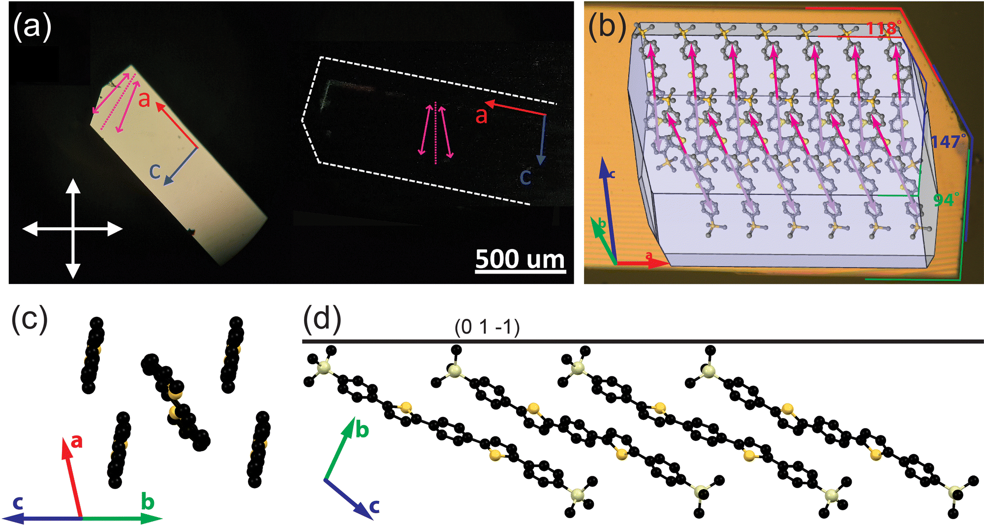 | ||
| Fig. 1 Structure of TMS-PTPTP-TMS crystals: (a) optical images of a crystal in crossed polarizers, purple arrows show projections of the calculated TDMs (ESI,† Section S2.1) on the largest crystal facet (01), and a dotted purple line indicates the bisectrix between their projections; (b) calculated crystal growth morphology collocated with an optical image of the crystal shown in panel (a): habit edges on the crystal image; red, blue and green lines and on the right indicate the angles between the crystal facets; (c) the herringbone arrangement of the molecules as viewed along the long molecular axes (the TMS groups and hydrogens are omitted for clarity); (d) view along the a-axis: the black line corresponds to the largest crystal facet with Miller indices (01), the molecules are oriented face-on with the long molecular axes (connecting carbons in the p-positions of the terminal phenylenes) inclined to the main crystal facet at 25° and 26°. | ||
The purple arrows in Fig. 1(b) show projections of the calculated molecular TDMs on the largest crystal facet. The non-collinear TDMs correspond to two non-equivalent molecules in the unit cell, and their projections form an angle of 19°. In the reminder of this paper, we will refer to TDMs as their projections on the largest crystal facet. The bisectrix between the non-collinear TDMs plotted by dotted lines in panels (a, b) are perfectly aligned (within 1°) with the polarizer orientation for the crystal oriented in the darkest position as shown in panel (b). Accordingly, the calculated TDM orientations fully correspond to the crystal images captured in the crossed polarizers.
Photoluminescence
Fig. 2 summarizes PL properties of TMS-PTPTP-TMS. Panel (a) shows PL image of a single crystal excited by a laser beam focused into point 1. As follows from the image, PL originates mainly from the excitation volume (area 1), whereas PL of much smaller intensity is emitted from the crystal edges (ESI,† Fig. S10a). This PL intensity difference is a consequence of face-on oriented molecules so that PL in the backward direction is radiated mainly from the excitation volume. Face-on oriented molecules strongly decrease the impact of PL waveguiding as compared with the edge-on ones (ESI,† Fig. S10). As follows from Fig. 2(a), PL from the excitation volume and the crystal edges has different colours quantified in the CIE 1931 chromaticity diagram (panel b). The colour of PL emitted from the excitation spot is blue, whereas that coming from the crystal edges is green. This difference is assigned to PL self-absorption, which predominantly suppresses the blue flank of the PL spectrum. The self-absorption is strongly pronounced for PL emitted from the crystal edges because the PL path length is about tens of microns in the waveguiding conditions.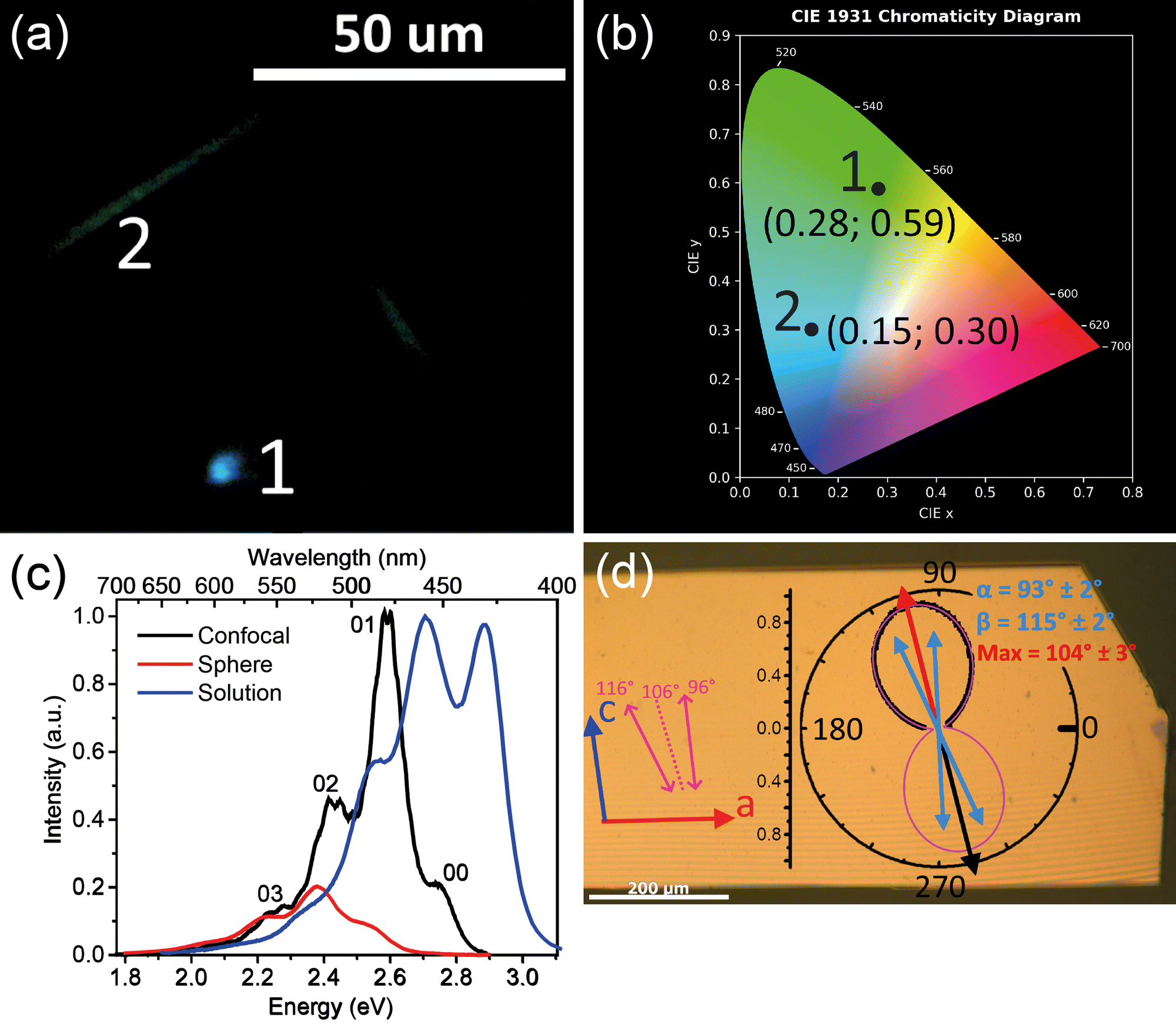 | ||
| Fig. 2 PL properties of TMS-PTPTP-TMS. (a) Optical image of a single crystal excited by a focused laser beam. White numerals mark PL from the laser beam spot (1) and from the crystal edges (2). (b) CIE 1931 chromaticity diagram: colour coordinates of the black dots corresponding to the numerals in panel (a). (c) PL spectra for diluted tetrahydrofuran solution (blue) from ref. 34, for a single crystal in the confocal configuration (black), and in the integrating sphere (red). The crystal spectra are scaled to align the PL intensities at the red flank (<2.35 eV, see the text). (d) Optical image of the crystal co-located with the PL polarization diagram. Stripes on the image are interference fringes. Red and blue arrows on the left represent the crystal axis, pink arrows and dashed pink line represent the TDM orientations and their bisectrix as described in Fig. 1; experimental PL polarization diagram is shown by black dots, two-TDMs fit is shown by the pink line; blue and red arrows represent orientations of the TDMs and their bisectrix, respectively. The angle values (α, β, and Max) and their uncertainties on the polarization diagram are the results of the fit (the details are given in ESI,† Section S6.4). | ||
Fig. 2(c) compares PL spectra of diluted solution (blue) and a single crystal recorded in the integrating sphere (red) and in the confocal configuration (black). The PL spectra of the crystals demonstrate a red shift by ∼0.15 eV relative to the solution spectrum. This shift is assigned to the intermolecular interactions, i.e., to the solid-state shift. The PL spectra show a clear vibrionic structure with apparent vibrational spacings in solution and crystals ∼0.15 eV, and this energy well agrees with the vibration energies of the thiophene rings in TPCOs.42 The very close vibrational spacings in solution and crystals indicates that the molecular packing in the solid state does not strongly affect the molecular geometry. For the spectrum recorded in the integrating sphere (red), the 00 band is completely suppressed, and the 01 and 02 bands are considerably less intensive as compared with the spectrum recorded in the confocal configuration (black). This effect is a result of PL self-absorption whose contribution in the spectra is much more pronounced for the spectrum recorded in the integrating sphere. In fact, in the confocal configuration, PL is collected mainly from the excitation volume, and therefore PL travels a path length about the excitation absorption length estimated as tens of nanometers.43 In contrast, the spectrum recorded in the integrating sphere is dominated by the contribution from the crystal edges. This follows from our spectral measurement, where PL excited by defocused UV-radiation was collected via the microscope objective separately from the crystal edge and from its largest facet (ESI,† Fig. S11). This measurement demonstrated that the crystal edge PL spectrum is significantly redshifted from that from the largest facet because of significant PL self-absorption. These two PL spectra are in good correspondence with the PL spectra recorded with the integrating sphere and in the confocal mode (Fig. 2(c)).
TMS-PTPTP-TMS is highly emissive in diluted solution, and its PL QY, Φ, was reported as high as Φ = 88 ± 4%.34 Remarkably, this material retains its high emissivity in the single crystal phase so that the PL QY value adjusted to self-absorption was evaluated as Φ = (82 ± 7)% (ESI,† Section S6.4) The PL transients perfectly corresponded to a monoexponential decay both in solution34 and crystal (ESI,† Fig. S20) with close decay times, τ, presented in Table 1. Consequently, the only emissive state, S1, is dominated in the photophysics of TMS-PTPTP-TMS.
The face-on molecular packing in TMS-PTPTP-TMS crystal is expected to result in J-aggregation. We calculated couplings between TDMs corresponding to all non-equivalent pairs of the neighbouring molecules in the crystal structure within the point-dipole approximation (ESI,† Section S2.2). These calculations showed that the only one molecular pair is H-aggregated with the strongest coupling, whereas all the other molecular pairs are J-aggregated with relatively weak couplings. Therefore, our calculations indicate that the total coupling corresponds to H-aggregation. This indication is supported by our experimental data, namely by the weakened 00 band in the crystal PL spectrum (Fig. 2(c)). This weakened band with the other signatures of H-aggregation are discussed in ESI,† Section S6.5.
The face-on arrangement of the molecules in TMS-PTPTP-TMS crystal (Fig. 1) should result in PL polarized according to the orientation of the molecular TDMs. More precisely, the PL polarization direction is expected to be oriented along the bisectrix between the TDMs as shown in Fig. 1(a) that is nearly along the c-axis.
Fig. 2(d) demonstrates PL polarization anisotropy of the single crystal excited by an excitation beam polarized along the bisectrix between TDMs. The 8-shape polarization diagram is oriented within 2° along the bisectrix (dotted line) between the calculated orientations of the TDMs. The axes ratio for the polarization diagram reaches 13.0 ± 0.3; therefore, PL emitted from the largest crystal facet is nearly linearly polarized with the polarization degree ρ = 0.86 ± 0.04. This is a consequence of face-on orientation of the molecules and perfectly agrees with the XRD data. A fitting model of two TDMs excited by the linearly polarized excitation (eqn (8) in ESI,† Section S6.4) nicely reproduces the PL polarization diagram so that the found orientations of the TDMs (the green arrows in panel d) are in very good agreement (within 4°) with those found from the crystal structure and DFT calculations (the pink arrows in panel d). The angle between the TDMs found from the fit is 22 ± 3°, and it coincides with that calculated from the DFT data (19°). Therefore, the calculated TDM orientations for the S0 → S1 transition (absorption) coincide with that corresponding to S1 → S0 transition (emission). This is in full agreement with the Condon approximation stating that the absorption and emission TDMs are equal for a given transition. Note that the PL spectra recorded at the minimum and maximum of the polarization diagram in Fig. 2(d) are indistinguishable (ESI,† Fig. S14). Consequently, they correspond to the same emissive state.
From the above analysis of the PL polarization features and XRD data, we conclude that the mutual TDM orientation of symmetrically independent molecules in the crystal unit cell fully determines the polarization properties of surface emission from the crystal. Accordingly, to maximize the polarization degree (ρ), one needs crystals with one molecule per their unit cell with in-plane orientation of its TDM. In contrast, orthogonally oriented two in-plane TDMs in a crystal unit cell should provide unpolarized surface emission with the zero ρ value.
Devices: charge transport and electroluminescence
The HOMO energies evaluated from the cyclic voltammetry measurements of TMS-PTPTP-TMS were −5.4 eV for solution and −5.7 eV for the deposit (ESI,† Fig. S6). Taking this into account, the hole injection contacts based on graphite (the work function 4.5–5 eV) and MoO3/Ag (the work function >5.3 eV) seem to be a reasonable choice for solution and vapor-processed TMS-PTPTP-TMS devices, respectively.Our charge-carrier mobility calculations predicted that the hole and electron mobilities should be 0.02 and 0.08 cm2 V−1 s−1, respectively. The unipolar hole-only OFETs prepared on free-standing single-crystals in the TCTG architecture with graphite electrodes and parylene gate dielectric demonstrated the maximal and average hole mobility of 0.054 and 0.03 cm2 V−1 s−1 in the saturation regime, which is in good agreement with the theoretically calculated one. These charge-carrier mobilities are within the range reported for other TPCO single crystals.18,20,23,35
To evaluate the potential of TMS-PTPTP-TMS in OLETs, first thin-film TCBG devices with asymmetric Ca and MoO3/Ag electrodes were studied because of their easier fabrication as compared with the corresponding single-crystal devices. Fig. 3(a) shows image of an operating thin-film OLET, and Fig. 3(b) demonstrates its typical transfer characteristics (the corresponding output characteristics are shown in the ESI,† Fig. S26a, and other details in Section S8.1). As the EL image in Fig. 3a is a superposition of EL images captured in various points of the transfer characteristics, it shows in one shot EL in both unipolar regimes—the blue stripes near the left (S) and right (D) electrodes correspond to the electron and hole unipolar regimes, respectively; and in the ambipolar regime—the blue stirpes in the channel. The movement of the EL zone position with change in VG (Fig. 3(a)) is a direct visualization and proof of the ambipolar regime.2 Moreover, the transfer characteristics is V-shaped indicating that the TMS-PTPTP-TMS material supports ambipolar charge transport. The estimated maximal and average hole mobilities in the linear regime were 2.3 × 10⁻⁵ and (1 ± 0.1) × 10−5 cm2 V−1 s−1, respectively; with the average threshold voltage for holes of –13 ± 14 V. The maximal and average electron mobilities were 5.2 × 10⁻⁵ and (1.8 ± 0.3) × 10−5 cm2 V−1 s−1, respectively; with the average threshold voltage for electrons of 46 ± 19 V. Accordingly, the hole and electron charge mobility are well balanced, which is beneficial for OLETs. Apparently, these charge-carrier mobility values are limited by the polycrystalline nature of the device active layers. Nevertheless, the ratio of the experimental hole and electron mobilities is in a reasonable agreement with that of the theoretical charge-carrier mobilities (1![[thin space (1/6-em)]](https://www.rsc.org/images/entities/char_2009.gif) :4).
:4).
 | ||
| Fig. 3 Thin-film OLET. (a) Image of a device with asymmetric source (MoO3/Ag) and drain (Ca) electrodes in the TCBG architecture with the channel length of 21 μm. This image is a superposition of a black and white image under the backlight and an EL image (its blue colour corresponds to the CIE 1931 chromaticity diagram) captured in dark with a long exposure (60 s) during the transfer characteristics measurement in both forward and backward direction with the voltage step of 2.5 V, red lines indicate stripe-like EL regions in the OLET channel at the corresponding VG values. (b) OLET transfer characteristics and the corresponding EL EQE vs. VG dependence. (c) EL spectra of thin-film and MC OLETs, the single-crystal PL spectrum recorded in the confocal configuration from Fig. 2(c) is shown for comparison. | ||
The EL EQE reached 1% near the minimum current (Fig. 3(b)), i.e., in the ambipolar regime. This EQE value is a good result for fluorescent OLETs without photonic structures enhancing light outcoupling24,44,45 and well agrees with the PL quantum yield reported above (see the discussion in ESI,† Section S8.4). For the thin-film OLET, the lower estimate luminance is about 2 cd m−2 (assuming the emission zone width of 1 μm as the higher estimate determined by the spatial resolution of the EL collection system), and the luminous efficiency is 0.4 cd A−1.
As follows from Fig. 3(c), the EL spectrum of the thin-film OLET and PL spectrum of the single crystal show very similar shapes. The less intensive blue part of the EL spectra is assigned to EL absorption by the OLET active layer as EL is generated near the interface of the active layer with the gate dielectric and hence travels the whole active-layer thickness. In contrast, PL was collected from the side of the crystal surface and therefore is less affected by self-absorption.
OLET samples based on MCs grown on the device substrate were used to study the EL polarization properties. The BCBG device architecture was used with EL collection from the top of the active layer (ESI,† Fig. S1). These device architecture and EL collection geometry were chosen to minimize the impact of electrodes on EL, which is expected to be strong for the devices emitting near their electrodes. The output and transfer characteristics of a BCBG MC OLET with symmetric Au electrodes are given in ESI,† Fig. S26b and c. The hole transport dominated in these devices, and the maximal and average hole mobilities were 0.024 and 0.0027 ± 0.0005 cm2 V−1 s−1, respectively; with the average threshold voltage equal to −18 ± 9 V. The maximal current in the MC OLET (ESI,† Fig. S26c) was about five orders higher than the ambipolar current in the thin-film OLET (Fig. 3(b)). As a result, the MC devices demonstrated strong EL: Fig. 4(a) shows a typical operating OLET sample with elongated TMS-PTPTP-TMS crystals lying on top of the electrodes. The estimated EL EQE of the MC OLETs was considerably lower (∼10−4–10−3%) than that of the thin-film OLETs because of the unipolar character of the MC devices so that EL occurred near the electrode, which can essentially quench EL. The EL spectra of the MC and thin-film OLETs are close (Fig. 3(c)), but the former has a weaker blue part because of stronger EL absorption resulting from the much thicker active layer whose thickness was in the range of 100–900 nm.
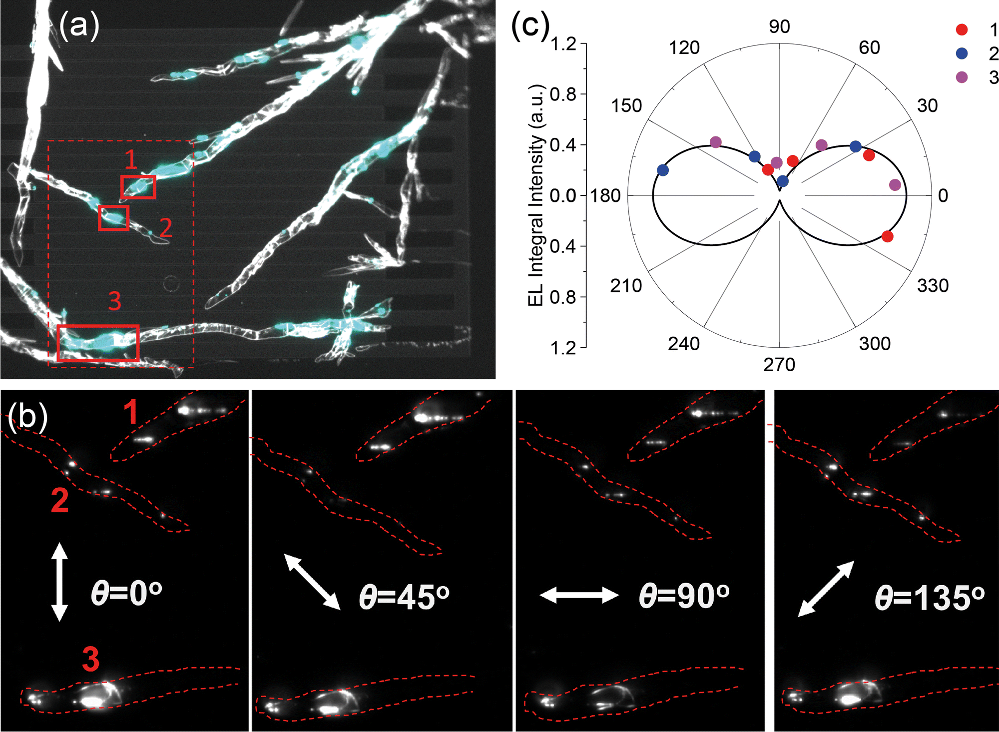 | ||
| Fig. 4 Polarization properties of EL emitted by a MC OLET. (a) Black-and-white OLET image (700 × 540 μm) under backlight with a superimposed coloured EL image captured without the polarizer at VD = −50 V and VG sweep from 10 V to −50 V and back, solid red rectangles denote three differently oriented crystals 1–3; (b) EL images of the region denoted by a dashed red rectangle in panel (a) at four different orientations of the polarizer; (c) cumulative EL polarization diagram for the three crystals from panel (b): the red, blue and pink dots represent crystals 1, 2, and 3, respectively; the black curve is a fit to the experimental data (the details are given in ESI,† Section S8.3). | ||
To study the EL polarization properties, the polarizer was placed between the MC OLET sample and the objective lens as shown in ESI,† Fig. S1. Panels (b and c) in Fig. 4 summarize our EL polarization studies. Images of the OLET channel during the device operation in dark were captured at different values of the polarizer orientation angle, θ. Panel (b) shows images of three crystals (marked with a solid red dashed line in panel a) for four different values of θ. As follows from these images, the EL intensity is the weakest when the polarizer axis is approximately collinear with the longest crystal edge corresponding to the a-axis (Fig. 1) and the brightest when the polarizer axis is nearly perpendicular to it. The former/latter corresponds to approximately codirectional/orthogonal orientations of the polarizer axis with respect to the orientation of molecular TDMs and the PL polarization (Fig. 1). From the OLET images shown in Fig. 4(b) the relative EL intensities for crystals 1–3 at different values of θ were calculated, and the dependences of these EL intensities on θ are presented for each crystal in ESI,† Fig. S27, and for all the crystals are summarized in Fig. 4(c). The maximal ratio of EL intensities of the two mutually perpendicular components was observed for crystal 2 and equals 8.2 ± 2.4; therefore, the corresponding polarization degree is ρ = 0.78 ± 0.06. The fit in Fig. 4(c) was done for the angle between the TDMs obtained from the PL polarization measurements (22°). Accordingly, as expected, the PL and EL polarization data are in excellent agreement. To the best of our knowledge, this is the first observation of strongly polarized surface EL from an OLET.
Conclusions
In this paper, we have extended the concept of strongly polarized surface EL to organic light-emitting transistors. TMS-PTPTP-TMS molecules were crystallized from solution in platy crystals with face-on molecular packing promoted by bulky terminal substituents (TMS groups). We have found that the polarization properties of light emission, both PL and EL, are fully controlled by the mutual orientations of the TDMs of symmetrically independent molecules in the crystal unit cell. Remarkably, TMS-PTPTP-TMS single crystals have been found to be highly emissive despite weak H-aggregation, contrary to the common belief that J-aggregation is required. Furthermore, we have demonstrated that the face-on molecular packing weakens light waveguiding and enhances surface emission. The TMS-PTPTP-TMS material has shown ambipolar charge transport with balanced electron and hole mobilities, which are beneficial for electronic light-emitting devices.TMS-PTPTP-TMS is, to the best of our knowledge, the first example of an almost totally emissive organic semiconductor with nearly in-plane oriented TDMs that supports balanced ambipolar charge transport, weakened light waveguiding, and strongly polarized surface emission. Thus, the rational molecular design of bulky-substituted highly emissive conjugated molecules appears to be a promising avenue towards high-performance single-crystal light-emitting devices.
Author contributions
V. A. Tr., A. V. K., and D. I. D. contributed equally to this work. O. V. B. synthesized the molecules, and S. A. P. supervised the synthetic part of the work; A. Y. S. calculated molecular and charge-transport properties; D. I. D. did high-vacuum sublimation, calculated crystal growth habits, dimers interactions, and intermolecular energies; V. A. Taf. performed XRD analysis, and T. V. R. processed the XRD data; M. S. K. did CV characterization, fabricated and studied single-crystal top-gate OFETs; V. A. Tr. fabricated OFET/OLET devices and studied them; A. V. K. did PL microscopy studies; V. G. K. grew crystals and measured their PL quantum yield; A. L. M. and A. A. M. carried out time-resolved PL studies under supervision by M. S. P.; D. Y. P. and M. S. P. conceptualized the study; S. A. P., M. S. P., and D. Y. P. developed and supervised the project. V. A. Tr., A. V. K., and D. Y. P. wrote the manuscript with the contributions from all the authors.Conflicts of interest
There are no conflicts to declare.Acknowledgements
This work (except the CV and TCTG OFET studies) was supported by the Russian Science Foundation (grant #18-12-00499) and was performed in the Enikolopov Institute of Synthetic Polymer Materials of Russian Academy of Sciences. The CV and TCTG OFET studies were supported by the Russian Science Foundation (project #20-73-10090). The steady-state PL studies were done by using the equipment purchased under the Lomonosov Moscow State University Program of Development. A. L. M. thanks the Erasmus+ Program for (partial) financial support of PL studies at Rijksuniversiteit Groningen in 2019. We acknowledge A. A. Mannanov for his participation at the initial stage of the project. We thank V. A. Postnikov for sharing his first growth experience of TMS-PTPTP-TMS crystals.Notes and references
- M. Muccini, A bright future for organic field-effect transistors, Nat. Mater., 2006, 5, 605–613 CrossRef CAS PubMed
.
- J. Zaumseil, R. H. Friend and H. Sirringhaus, Spatial control of the recombination zone in an ambipolar light-emitting organic transistor, Nat. Mater., 2006, 5, 69–74 CrossRef CAS
- K. Sawabe, M. Imakawa, M. Nakano, T. Yamao, S. Hotta, Y. Iwasa and T. Takenobu, Current-Confinement Structure and Extremely High Current Density in Organic Light-Emitting Transistors, Adv. Mater., 2012, 24, 6141–6146 CrossRef CAS PubMed
- J.-S. Kim, P. K. H. Ho, N. C. Greenham and R. H. Friend, Electroluminescence emission pattern of organic light-emitting diodes: Implications for device efficiency calculations, J. Appl. Phys., 2000, 88, 1073–1081 CrossRef CAS
- K. S. Whitehead, M. Grell, D. D. C. Bradley, M. Inbasekaran and E. P. Woo, Polarized emission from liquid crystal polymers, Synth. Met., 2000, 111–112, 181–185 CrossRef CAS
- J. R. Brandt, X. Wang, Y. Yang, A. J. Campbell and M. J. Fuchter, Circularly Polarized Phosphorescent Electroluminescence with a High Dissymmetry Factor from PHOLEDs Based on a Platinahelicene, J. Am. Chem. Soc., 2016, 138, 9743–9746 CrossRef CAS PubMed
- H.-Y. Huang, Y.-F. Zhu, F. Nan, G.-H. Zhou, Y. Lin, Y.-L. Ma and L. Zhou, Polarized electroluminescence from organic light-emitting diodes with simultaneously integrated random nanohole arrays and metal nanograting, Opt. Mater., 2021, 116, 111106 CrossRef CAS
- D. Y. Kim, Potential application of spintronic light-emitting diode to binocular vision for three-dimensional display technology, J. Korean Phys. Soc., 2006, 49, S505–S508 Search PubMed
- M. Y. Lin, H. H. Chen, K. H. Hsu, Y. H. Huang, Y. J. Chen, H. Y. Lin, Y. K. Wu, L. A. Wang, C. C. Wu and S. C. Lee, White Organic Light-Emitting Diode With Linearly Polarized Emission, IEEE Photonics Technol. Lett., 2013, 25, 1321–1323 CAS
- Y. Yomogida, H. Sakai, K. Sawabe, S. Gocho, S. Z. Bisri, H. Nakanotani, C. Adachi, T. Hasobe, Y. Iwasa and T. Takenobu, Multi-color light-emitting transistors composed of organic single crystals, Org. Electron., 2013, 14, 2737–2742 CrossRef CAS
- S. Qu, Q. Lu, S. Wu, L. Wang and X. Liu, Two dimensional directed π–π interactions in a linear shaped bi-1,3,4-oxadiazole derivative to achieve organic single crystal with highly polarized fluorescence and amplified spontaneous emissions, J. Mater. Chem., 2012, 22, 24605–24609 RSC
- H. Mizuno, T. Maeda, H. Yanagi, H. Katsuki, M. Aresti, F. Quochi, M. Saba, A. Mura, G. Bongiovanni, F. Sasaki and S. Hotta, Optically Pumped Lasing from Single Crystals of a Cyano-Substituted Thiophene/Phenylene Co-Oligomer, Adv. Opt. Mater., 2014, 2, 529–534 CrossRef CAS
- M. Wang, Y. Gong, F. Alzina, C. M. Sotomayor Torres, H. Li, Z. Zhang and J. He, Angle-Dependent Photoluminescence Spectroscopy of Solution-Processed Organic Semiconducting Nanobelts, J. Phys. Chem. C, 2017, 121, 12441–12446 CrossRef CAS
- C. Mayr, T. D. Schmidt and W. Brütting, High-efficiency fluorescent organic light-emitting diodes enabled by triplet-triplet annihilation and horizontal emitter orientation, Appl. Phys. Lett., 2014, 105, 183304 CrossRef
- H. Nakanotani, M. Saito, H. Nakamura and C. Adachi, Emission Color Tuning in Ambipolar Organic Single-Crystal Field-Effect Transistors by Dye-Doping, Adv. Funct. Mater., 2010, 20, 1610–1615 CrossRef CAS
- S. Hotta and T. Yamao, The thiophene/phenylene co-oligomers: exotic molecular semiconductors integrating high-performance electronic and optical
functionalities, J. Mater. Chem., 2011, 21, 1295–1304 RSC
- T.-W. Koh, J. A. Spechler, K. M. Lee, C. B. Arnold and B. P. Rand, Enhanced Outcoupling in Organic Light-Emitting Diodes via a High-Index Contrast Scattering Layer, ACS Photonics, 2015, 2, 1366–1372 CrossRef CAS
- S. Hotta, T. Yamao, S. Z. Bisri, T. Takenobu and Y. Iwasa, Organic single-crystal light-emitting field-effect transistors, J. Mater. Chem. C, 2014, 2, 965–980 RSC
- S. K. Park, J. H. Kim, T. Ohto, R. Yamada, A. O. F. Jones, D. R. Whang, I. Cho, S. Oh, S. H. Hong, J. E. Kwon, J. H. Kim, Y. Olivier, R. Fischer, R. Resel, J. Gierschner, H. Tada and S. Y. Park, Highly Luminescent 2D-Type Slab Crystals Based on a Molecular Charge-Transfer Complex as Promising Organic Light-Emitting Transistor Materials, Adv. Mater., 2017, 29, 7 Search PubMed
- M. S. Kazantsev, E. S. Frantseva, L. G. Kudriashova, V. G. Konstantinov, A. A. Mannanov, T. V. Rybalova, E. V. Karpova, I. K. Shundrina, G. N. Kamaev, M. S. Pshenichnikov, E. A. Mostovich and D. Y. Paraschuk, Highly-emissive solution-grown furan/phenylene co-oligomer single crystals, RSC Adv., 2016, 6, 92325–92329 RSC
- M. S. Kazantsev, A. A. Beloborodova, A. D. Kuimov, I. P. Koskin, E. S. Frantseva, T. V. Rybalova, I. K. Shundrina, C. S. Becker and E. A. Mostovich, Synthesis, luminescence and charge transport properties of furan/phenylene co-oligomers: The study of conjugation length effect, Org. Electron., 2018, 56, 208–215 CrossRef CAS
- A. A. Mannanov, M. S. Kazantsev, A. D. Kuimov, V. G. Konstantinov, D. I. Dominskiy, V. A. Trukhanov, D. S. Anisimov, N. V. Gultikov, V. V. Bruevich, I. P. Koskin, A. A. Sonina, T. V. Rybalova, I. K. Shundrina, E. A. Mostovich, D. Y. Paraschuk and M. S. Pshenichnikov, Long-range exciton transport in brightly fluorescent furan/phenylene co-oligomer crystals, J. Mater. Chem. C, 2019, 7, 60–68 RSC
- A. Y. Sosorev, V. A. Trukhanov, D. R. Maslennikov, O. V. Borshchev, R. A. Polyakov, M. S. Skorotetcky, N. M. Surin, M. S. Kazantsev, D. I. Dominskiy, V. A. Tafeenko, S. A. Ponomarenko and D. Y. Paraschuk, Fluorinated Thiophene-Phenylene Co-Oligomers for Optoelectronic Devices, ACS Appl. Mater. Interfaces, 2020, 12, 9507–9519 CrossRef CAS PubMed
- I. P. Koskin, C. S. Becker, A. A. Sonina, V. A. Trukhanov, N. A. Shumilov, A. D. Kuimov, Y. S. Zhuravleva, Y. O. Kiseleva, I. K. Shundrina, P. S. Sherin, D. Y. Paraschuk and M. S. Kazantsev, Selectively Fluorinated Furan-Phenylene Co-Oligomers Pave the Way to Bright Ambipolar Light-Emitting Electronic Devices, Adv. Funct. Mater., 2021, 31, 2104638 CrossRef CAS
- R. Fedorenko, A. Kuevda, V. A. Trukhanov, A. Y. Sosorev, A. V. Bakirov, A. I. Dorokhov, N. Surin, O. Borshchev, S. Ponomarenko and D. Paraschuk, Luminescent 2D single crystals of thiophene-phenylene co-oligomers for field-effect devices, Mater. Chem. Front., 2022, 6, 3279–3295 RSC
- R. S. Fedorenko, A. V. Kuevda, V. A. Trukhanov, V. G. Konstantinov, A. Y. Sosorev, A. A. Sonina, M. S. Kazantsev, N. M. Surin, S. Grigorian, O. V. Borshchev, S. A. Ponomarenko and D. Y. Paraschuk, Luminescent High-Mobility 2D Organic Semiconductor Single Crystals, Adv. Electron. Mater., 2022, 8, 2101281 CrossRef CAS
- A. A. Sonina, I. P. Koskin, P. S. Sherin, T. V. Rybalova, I. K. Shundrina, E. A. Mostovich and M. S. Kazantsev, Crystal packing control of a trifluoromethyl-substituted furan/phenylene co-oligomer, Acta Crystallogr., Sect. B: Struct. Sci., Cryst. Eng. Mater., 2018, 74, 450–457 CrossRef CAS PubMed
- J. Gierschner, J. Shi, B. Milián-Medina, D. Roca-Sanjuán, S. Varghese and S. Park, Luminescence in Crystalline Organic Materials: From Molecules to Molecular Solids, Adv. Opt. Mater., 2021, 9, 2002251 CrossRef CAS
- H. Mizuno, T. Jinjyo, K. Bando, F. Sasaki, K. Yamashita and H. Yanagi, Impact of material parameters on strong exciton–photon coupling states formed in microcrystal resonators of p- and n-type thiophene/phenylene co-oligomers, J. Mater. Chem. C, 2021, 9, 11189–11197 RSC
- V. A. Postnikov, Y. I. Odarchenko, A. V. Iovlev, V. V. Bruevich, A. Y. Pereverzev, L. G. Kudryashova, V. V. Sobornov, L. Vidal, D. Chernyshov, Y. N. Luponosov, O. V. Borshchev, N. M. Surin, S. A. Ponomarenko, D. A. Ivanov and D. Y. Paraschuk, Molecularly Smooth Single-Crystalline Films of Thiophene–Phenylene Co-Oligomers Grown at the Gas–Liquid Interface, Cryst. Growth Des., 2014, 14, 1726–1737 CrossRef CAS
- M. S. Kazantsev, A. A. Beloborodova, E. S. Frantseva, T. V. Rybalova, V. G. Konstantinov, I. K. Shundrina, D. Y. Paraschuk and E. A. Mostovich, Methyl substituent effect on structure, luminescence and semiconducting properties of furan/phenylene co-oligomer single crystals, CrystEngComm, 2017, 19, 1809–1815 RSC
- J. Zaumseil and H. Sirringhaus, Electron and ambipolar transport in organic field-effect transistors, Chem. Rev., 2007, 107, 1296–1323 CrossRef CAS PubMed
- J. Zaumseil, Recent Developments and Novel Applications of Thin Film, Light-Emitting Transistors, Adv. Funct. Mater., 2020, 30, 1905269 CrossRef CAS
- T. Y. Starikova, N. M. Surin, O. V. Borshchev, S. A. Pisarev, E. A. Svidchenko, Y. V. Fedorov and S. A. Ponomarenko, A novel highly efficient nanostructured organosilicon luminophore with unusually fast photoluminescence, J. Mater. Chem. C, 2016, 4, 4699–4708 RSC
- O. D. Parashchuk, A. A. Mannanov, V. G. Konstantinov, D. I. Dominskiy, N. M. Surin, O. V. Borshchev, S. A. Ponomarenko, M. S. Pshenichnikov and D. Y. Paraschuk, Molecular Self-Doping Controls Luminescence of Pure Organic Single Crystals, Adv. Funct. Mater., 2018, 28, 1800116 CrossRef
-
T. B. Paolini, SpectraChroma, 2021 DOI:10.5281/zenodo.4906590
- G. M. Sheldrick, A short history of SHELX, Acta Crystallogr., Sect. A: Found. Crystallogr., 2008, 64, 112–122 CrossRef CAS PubMed
- M. S. Kazantsev, V. A. Postnikov, V. G. Konstantinov, O. V. Borshchev, T. V. Rybalova, V. V. Bruevich, V. A. Tafeenko, S. A. Ponomarenko and D. Y. Paraschuk, CCDC 1465146,† CSD Communication, 2017.
- M. W. Schmidt, K. K. Baldridge, J. A. Boatz, S. T. Elbert, M. S. Gordon, J. H. Jensen, S. Koseki, N. Matsunaga, K. A. Nguyen, S. Su, T. L. Windus, M. Dupuis and J. A. Montgomery Jr, General atomic and molecular electronic structure system, J. Comput. Chem., 1993, 14, 1347–1363 CrossRef CAS
- Chemcraft – graphical software for visualization of quantum chemistry computations, https://www.chemcraftprog.com.
- T. Yamao, T. Miki, H. Akagami, Y. Nishimoto, S. Ota and S. Hotta, Direct Formation of Thin Single Crystals of Organic Semiconductors onto a Substrate, Chem. Mater., 2007, 19, 3748–3753 CrossRef CAS
- A. Y. Sosorev, M. K. Nuraliev, E. V. Feldman, D. R. Maslennikov, O. V. Borshchev, M. S. Skorotetcky, N. M. Surin, M. S. Kazantsev, S. A. Ponomarenko and D. Y. Paraschuk, Impact of terminal substituents on the electronic, vibrational and optical properties of thiophene–phenylene co-oligomers, Phys. Chem. Chem. Phys., 2019, 21, 11578–11588 RSC
-
A. A. Mannanov, Photoluminescence and Raman Spectroscopy of Highly Ordered Organic Semiconductor Structures, PhD thesis, Rijksuniversiteit Groningen, 2019
- M. C. Gwinner, D. Kabra, M. Roberts, T. J. K. Brenner, B. H. Wallikewitz, C. R. McNeill, R. H. Friend and H. Sirringhaus, Highly Efficient Single-Layer Polymer Ambipolar Light-Emitting Field-Effect Transistors, Adv. Mater., 2012, 24, 2728–2734 CrossRef CAS PubMed
- M. Natali, S. D. Quiroga, L. Passoni, L. Criante, E. Benvenuti, G. Bolognini, L. Favaretto, M. Melucci, M. Muccini, F. Scotognella, F. Di Fonzo and S. Toffanin, Simultaneous Tenfold Brightness Enhancement and Emitted-Light Spectral Tunability in Transparent Ambipolar Organic Light-Emitting Transistor by Integration of High-k Photonic Crystal, Adv. Funct. Mater., 2017, 27, 1605164 CrossRef
Footnote |
| † Electronic supplementary information (ESI) available. CCDC 1465146. For ESI and crystallographic data in CIF or other electronic format see DOI: https://doi.org/10.1039/d2qm01046a |
| This journal is © the Partner Organisations 2023 |