
 Open Access Article
 This Open Access Article is licensed under a Creative Commons Attribution-Non Commercial 3.0 Unported Licence
Recent progress of the single crystal growth of homologous (InGaO3)m(ZnO)n
Naoki
Kase
*a,
Noboru
Kimizuka
b and
Nobuaki
Miyakawa
 *a
*a
aDepartment of Applied Physics, Tokyo University of Science, 6-3-1 Niijuku, Katsushika-ku, Tokyo 125-8585, Japan. E-mail: n-kase@rs.tus.ac.jp; miyakawa@rs.tus.ac.jp
bDepartamento de Investigación en Polímeros y Materiales, Universidad de Sonora, Rosales y Luis Encinas s/n, Hermosillo, Sonora CP 83000, Mexico
First published on 10th June 2022
Abstract
Compounds composed of In–Ga–Zn–O (IGZO) have characteristic homologous crystal structures represented by the following general formula: (InGaO3)m(ZnO)n. Such compounds have been applied in many fields since the discovery that amorphous oxide thin films have high electron mobility. On the other hand, very few studies have been conducted on single crystals or the bulk behavior of IGZO compounds as growing large crystals is difficult. Consequently, the physical properties have not been clarified. In this review, we summarize the historical background of IGZO regarding the crystal structure and crystal growth, and introduce our successful method for growing large single crystals of InGaZnO4. We also introduce the micro-crystals of (InGaO3)2(ZnO)1.
1 Introduction
Renewable energy production from sources such as solar and wind power has attracted considerable attention. The use of metal oxide semiconductors that reduce thermal energy is expected to be an important step in such energy production. Transparent amorphous-oxide semiconductors from the In–Ga–Zn–O (IGZO) series have been proposed as candidates for the active channel in transparent thin-film transistors (TFTs)1,2 and are currently employed in various display devices.3–5 IGZO-based field-effect transistors (FETs) can be used to produce devices with extremely low power consumption compared with modern Si-based devices.1,2,6–8 The oxide semiconductors with the nearly zero off-state current, could be one of the trump cards to solve energy problems, as they can achieve devices with the extremely lower power consumption compared to cutting-edge Si-based devices.In 2003, Nomura et al. reported the fabrication of transparent FETs with a single crystalline layer of InGaO3(ZnO)5 as the channel.1 In 2004, they demonstrated the promising potential of amorphous metal oxides as transparent TFT semiconductors.2 When post-transition metals are used, the direct overlap of the isotropic s-orbitals is large and not significantly affected even in an amorphous structure. Amorphous-IGZO (a-IGZO) thin films have emerged as a particularly promising structure with Hall mobilities of up to 40 cm2 V−1 s−1 and practical field effect mobilities of 10 cm2 V−1 s−1.2 These mobilities are the result of an omnidirectional carrier transport path, which is dominated by the s-orbitals of the cation, and these values are an order of magnitude larger than those recorded for amorphous Si (a-Si). Furthermore, the feature of the device fabricated on the polyethylene terephthalate sheet is flexible and can be bent. The characteristics are stable even after repeated bending of the transparent TFT sheet.
In 2009, a new layered crystalline structure type was discovered, known as c-axis-aligned crystalline IGZO (CAAC-IGZO),9,10 in which the elemental arrangement is strongly oriented along the c-axis of the three crystal axes. The extremely low off-state current (Ioff) produced in FETs fabricated by using CAAC-IGZO make the design of electronic devices with significantly low power consumption, called metal-oxide-semiconductor field-effect transistors (MOSFETs), possible. MOSFETs developed by using CAAC-IGZO can exhibit an extremely low off-state current per micrometer of 10−24 A μm−1 (ref. 11–14) and high mobilities of 30–70 cm2 V−1 s−1 when the composition ratio is changed. The off-state current is considerably smaller than that of a-Si (10−12 A μm−1).
The crystal phase of the In–Ga–Zn–O series was first recognized by Kimizuka et al. in 1985.15 They reported phase relationships and solubility ranges by using powder X-ray diffraction (XRD) data of the homologous InGaO3(ZnO)n compounds (n = 1–13).15–20 The structure consisted of stacked metal oxide layers along the c-axis of a trigonal (even values of n) or hexagonal (odd values of n) unit cell. Several homologous compounds of the oxides of ARO3(MO)n (M = Mg, Mn, Fe, Co, Cu, Zn, and Cd; A = Sc, Y, In, Ho, Er, Tm, Yb, and Lu; R = Al, Fe, and Ga) were characterized.21–25
Two types of homologous compounds in the IGZO-series are reported: InGaO3(ZnO)n and (InGaO3)mZnO. Both homologous structures are layered and have a common structural unit. The crystal structure of the InGaO3(ZnO)n homologous series consists of (i) edge sharing InO6 octahedra, (ii) wurtzite-type ZnO4 tetrahedra, and (iii) trigonal bipyramidal GaO5. These compounds crystallize in space group R![[3 with combining macron]](https://www.rsc.org/images/entities/char_0033_0304.gif) m for n = odd and P63/mmc for n = even.26 In the case of n = odd, the number of InO6 layers is 3, and in the case of n = even, the number is 2. In contrast, for the (InGaO3)mZnO series, only m = 1 and 2 are reported.15 This type of homologous series has also been observed in compounds of (YbFeO3)mFeO,28–30 (InGaO3)mCuO,31 and In2S3(ZnS)1.32 Although the InO6 octahedral layers in the InGaO3(ZnO)n system are equidistance along the c-axis, these are not seen in the (InGaO3)2ZnO system. This is owing to the (InGaO3)2ZnO conformation having insufficient space for equal-sized wurtzite slabs between the octahedral layers.
m for n = odd and P63/mmc for n = even.26 In the case of n = odd, the number of InO6 layers is 3, and in the case of n = even, the number is 2. In contrast, for the (InGaO3)mZnO series, only m = 1 and 2 are reported.15 This type of homologous series has also been observed in compounds of (YbFeO3)mFeO,28–30 (InGaO3)mCuO,31 and In2S3(ZnS)1.32 Although the InO6 octahedral layers in the InGaO3(ZnO)n system are equidistance along the c-axis, these are not seen in the (InGaO3)2ZnO system. This is owing to the (InGaO3)2ZnO conformation having insufficient space for equal-sized wurtzite slabs between the octahedral layers.
Owing to recent progress in the measurement accuracy, certain physical properties can be determined on small single crystals.33–37 However, since the measurement methods are severely limited, a single crystal of sufficient size is required to evaluate bulk properties. In the past decade or so, studies have been conducted on the successful growth of small single crystals of the IGZO series, which are suitable for detailed crystal structure analysis. A large single crystal is required to perform sufficient measurements for elucidating the mechanism of the unusual transport phenomena of the IGZO series. In recent years, we have succeeded in growing large single crystals of IGZO compounds, and substantial progress has been made toward examining their physical properties. In this review, we introduce the recent progress in the growth of single crystals of compounds in the IGZO series.
2 Single-crystalline and c-axis-aligned crystal thin film
Several types of the IGZO thin films have been known so far. Hosono et al. reported that both amorphous- and single-crystalline IGZO thin films exhibit high-electron mobility in TFTs.1,2 Yamazaki et al. reported that CAAC-IGZO thin films can be used to produce highly reliable FETs.9–14 Here, we introduce the growth method and detailed structure of the single-crystalline IGZO and CAAC-IGZO thin films.2.1 Single-crystalline film
Using a conventional vapor-phase growth technique to fabricate single-crystalline thin films of metal oxides with a complex layered structure and composition is difficult. To solve this problem, a practical method for growing the single-crystalline thin films of the layered complex oxides was developed, called the “Reactive Solid-Phase Epitaxy (R-SPE) technique”.38–40Single-crystalline films of InGaO3(ZnO)n were grown by R-SPE as follows. Pulsed laser deposition (PLD) was used to deposit a 2 nm-thick ZnO epitaxial layer at 973 K (700 °C) on a (111) single-crystal yttria-stabilized zirconia (YSZ) substrate (the template), followed by a 120 nm-thick InGaO3(ZnO)5 layer at room temperature. Next, the bilayer film was annealed in an appropriate atmosphere, to obtain a single-crystalline film. The fabricated bilayer was covered with a YSZ plate to suppress evaporation of the film components and was then subjected to thermal annealing at 1673 K (1400 °C) for 30 min, resulting in the growth of its single-crystalline phase.
Fig. 1(B and C) show cross-sectional high-resolution transmission electron microscopy (HRTEM) images of the InGaO3(ZnO)5 film. The layered lattice structure with periodic stacking of InO2-layers and GaO(ZnO)5 blocks is clearly observed and is also found in the electron diffraction image. At the film–substrate interface there is less of this ordered stacking and observation of field-emission scanning electron microscopy (FESEM) images revealed no defect structure such as grain boundaries or dislocation over the entire area. It was concluded from these results that the epitaxial ZnO thin layer plays an essential role in controlling the crystallographic orientation, while the thickness ratio between the two layers controls the film composition.
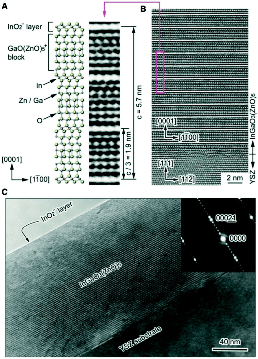 | ||
| Fig. 1 (A) Crystal structure of InGaO3(ZnO)5. The InO2 layer (In3+ ion is located at an octahedral site coordinated by oxygens) and the GaO(ZnO)5 blocks (Ga3+ and Zn2+ ions share trigonal–bipyramidal and tetrahedral sites) are alternately stacked along the [0001] direction at a period of 1.9 nm (A HRTEM lattice image is shown for comparison). (B and C) Cross-sectional HRTEM images of a InGaO3(ZnO)5 thin film grown on YSZ(111) by reactive solid-phase epitaxy. Periodic stacking of the InO2 layer and the GaO(ZnO)5 block is clearly visible and confirmed in the electron diffraction image. A single-crystalline film is formed over the entire observation area. The topmost layer of the film is the InO2-layer. Panels (A–C) are reprinted with permission from ref. 1. © 2019 American Physical Society. | ||
Single-crystal thin films of the InGaO3(ZnO)n series with n = 1–35 can also be fabricated by the R-SPE method.41 The thicknesses of the resultant InGaO3(ZnO)n films were 90–250 nm. As shown in Fig. 2(b), atomically flat terraced and stepped surfaces were observed in the topographic atomic force microscopy (AFM) image of the InGaO3(ZnO)5 film grown on a (111) YSZ substrate. Fig. 2(c and d) show a summary of the cross-sectional high angle annular dark field (HAADF) images of the InGaO(ZnO)15 single-crystalline film grown on a (111) YSZ substrate. A superlattice structure composed of InO-layers and GaO(ZnO)n blocks was periodically observed.
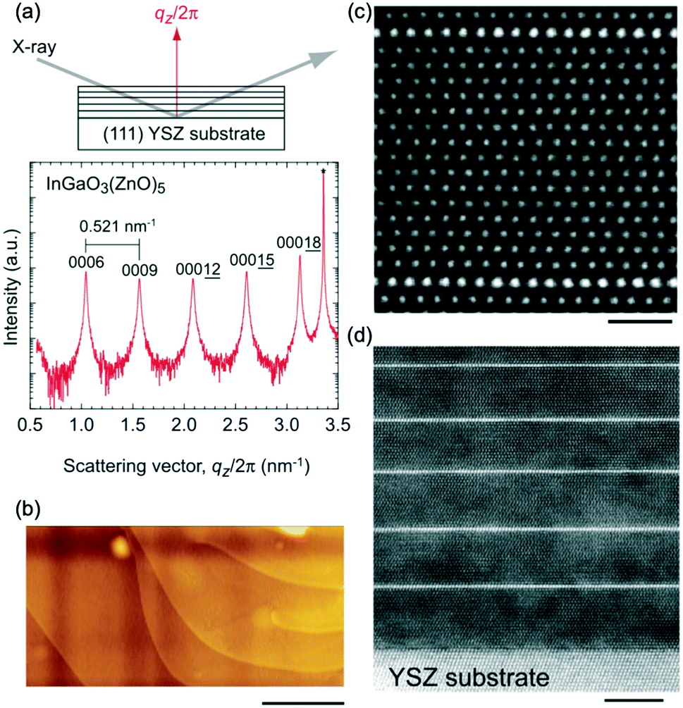 | ||
| Fig. 2 X-ray diffraction (XRD) data of the superlattices. (a) Out-of-plane XRD pattern of the resultant InGaO3(ZnO)5 film on a (111) YSZ substrate. The peak interval (0.521 nm−1) corresponds to the distance between two adjacent InO-layers (1.92 nm). (b) Topographic atomic force microscopy (AFM) images of InGaO3(ZnO)5 films on a (111) YSZ substrate (the scale bar is 500 nm). (c) Atomic arrangement of the superlattices. HAADF images of the resultant InGaO3(ZnO)15 film grown on a (111) YSZ single crystal substrate. Brighter lines of one-atomic-layer thickness are periodically present, corresponding to InO-layers. Atomic structure of the layered structure (scale bar = 1 nm). (d) The bottom part (scale bar = 5 nm). Panels (a–d) are reprinted with permission from ref. 41. © 2022 John Wiley and Sons, Inc. | ||
2.2 c-Axis-aligned crystalline film
In this section, we introduce the c-axis-aligned crystalline (CAAC) thin film. CAAC-IGZO was first discovered in 2009.9,10 The characteristic structure of CAAC-IGZO is a c-axis orientation perpendicular to the surface of the entire film but with no order in the ab-plane direction. The benefit of this structure is that the CAAC-IGZO films can be synthesized at a lower temperature than single-crystal thin films and stable production is possible.Films with thicknesses 100–300 nm were fabricated on quartz substrates by the sputtering method.9,10,42–44 A polycrystalline substance with In, Ga, and Zn at an atomic ratio of 1![[thin space (1/6-em)]](https://www.rsc.org/images/entities/char_2009.gif) :1:1 was used as the target. The conditions for dc-magnetron sputtering were as follows: the deposition power density was 0.87 W cm−1 and the deposition pressure was 0.4 Pa with a O2/(Ar + O2) gas flow rate of 0.33. The power density in ac-magnetron sputtering was 1.66 W cm−1 and the pressure was 0.6 Pa with O2/(Ar + O2) gas flow rate of 0.5. The deposition temperature necessary for the deposition of CAAC-IGZO was 423 K (150 °C). The temperature is lower than that of R-SPE method.
:1:1 was used as the target. The conditions for dc-magnetron sputtering were as follows: the deposition power density was 0.87 W cm−1 and the deposition pressure was 0.4 Pa with a O2/(Ar + O2) gas flow rate of 0.33. The power density in ac-magnetron sputtering was 1.66 W cm−1 and the pressure was 0.6 Pa with O2/(Ar + O2) gas flow rate of 0.5. The deposition temperature necessary for the deposition of CAAC-IGZO was 423 K (150 °C). The temperature is lower than that of R-SPE method.
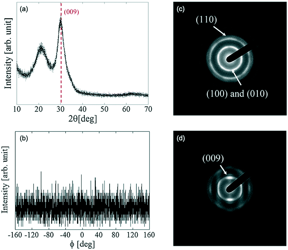
Fig. 3(a and b) show the in-plane and out-of-plane XRD spectra of the CAAC-IGZO film. The results show that the out-of-plane XRD spectrum of the fabricated IGZO film has a peak corresponding to a crystal at ∼31°. The peak corresponds to the (009) plane of a InGaZnO4 crystal, which indicates that the fabricated IGZO film differed from an amorphous structure. There was no evidence of symmetry in the (110) plane detected in the in-plane XRD images. Thus, it was concluded that there was no preferential orientation in the a-axis and b-axis directions, although the c-axis was aligned.
 | ||
| Fig. 3 XRD measurement results for c-axis-aligned crystalline In–Ga–Zn–O: (a) out-of-plane XRD spectra and (b) in-plane (ϕ-scan) XRD spectra (2θ = 56°). (c) SAED diffraction pattern of CAAC-IGZO in the perpendicular direction, and (d) in the parallel direction. Panels (a–d) are reprinted with permission from ref. 10. © 2014 Society for Information Display. | ||
Fig. 3(c and d) show the results of the selected area electron diffraction (SAED) measurements with an electron beam (beam diameter; 300 nm) positioned perpendicularly, then parallel to the substrate. In the images where the electron beam was incident perpendicularly, rings are clearly observed. The rings were ascribed to overlapped diffractions of the (010) and (100) planes of the InGaZnO4. In addition, a second ring originating from the (110) plane was also observed. By contrast, when the electron beam was parallel to the substrate, spots attributed to the (009) plane were observed. These results revealed that the c-axis of the CAAC-IGZO is aligned perpendicularly to the thin film.
3 Small single crystal
The growth of small single crystals of InGaO3(ZnO)n (n = 1–4) was reported by Mader et al., although the crystal size of n = 3 was not sufficiently large to perform single crystal analysis. These small crystals were unsuitable for measurements of physical properties but were sufficient for determining the detailed crystal structure. In this section, the explanation is divided into two situations, (1) where n is odd (n = 1, 3; Rm) and (2) where n is even (n = 2, 4; P63/mmc).
3.1 Small single crystal of IGZO-11 and IGZO-13
The growth of a small single crystal of IGZO-11 has been reported by two groups. The methods were using high-pressure synthesis45 and slow-cooling in a sealed Pt crucible.46 These single crystals of the InGaO3(ZnO)n (or IGZO-1n) are part of the homologous series where n is odd (n = 1, 3; Rm).
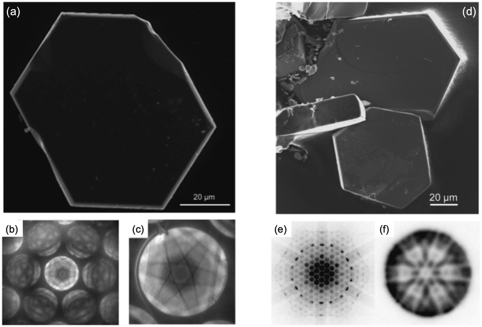
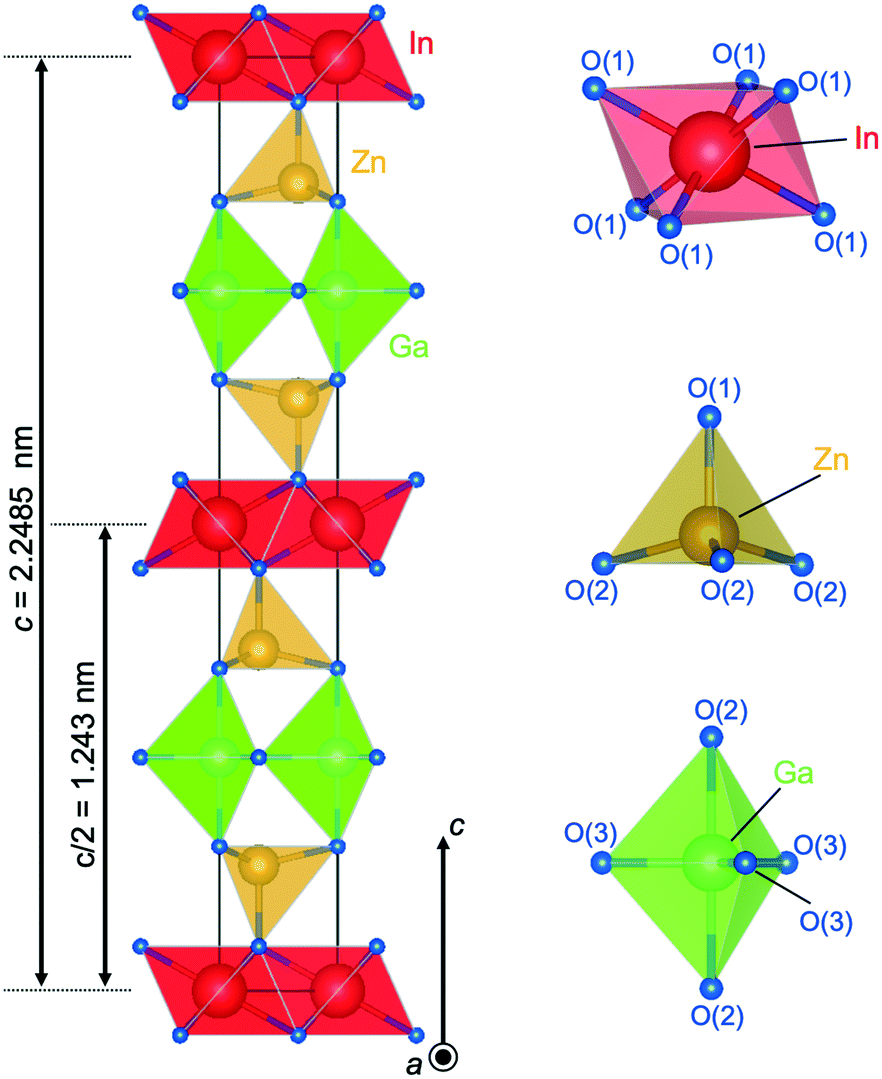
Fig. 4(a) shows the optical micrograph image of a crystal of IGZO-11. Bluish-gray transparent crystals were obtained as the product of the synthesis in addition to a small amount of colorless powder. The crystal was very small, but this was the largest available in the IGZO series at that time. A HAADF image at the [1![[1 with combining macron]](https://www.rsc.org/images/entities/char_0031_0304.gif) 00] orientation is shown in Fig. 4(b) with the structure model as overlay. The octahedral layers containing In appear with a strong contrast and have a distance from the (0003) lattice fringes of d = 0.868 nm, which agrees with the values from single crystal refinement data. The (20) prism planes with spacing of 0.164 nm are well resolved. The image IGZO-11 at atomic resolution in the electron microscope supports a perfect periodic stacking of atomic layers.
00] orientation is shown in Fig. 4(b) with the structure model as overlay. The octahedral layers containing In appear with a strong contrast and have a distance from the (0003) lattice fringes of d = 0.868 nm, which agrees with the values from single crystal refinement data. The (20) prism planes with spacing of 0.164 nm are well resolved. The image IGZO-11 at atomic resolution in the electron microscope supports a perfect periodic stacking of atomic layers.
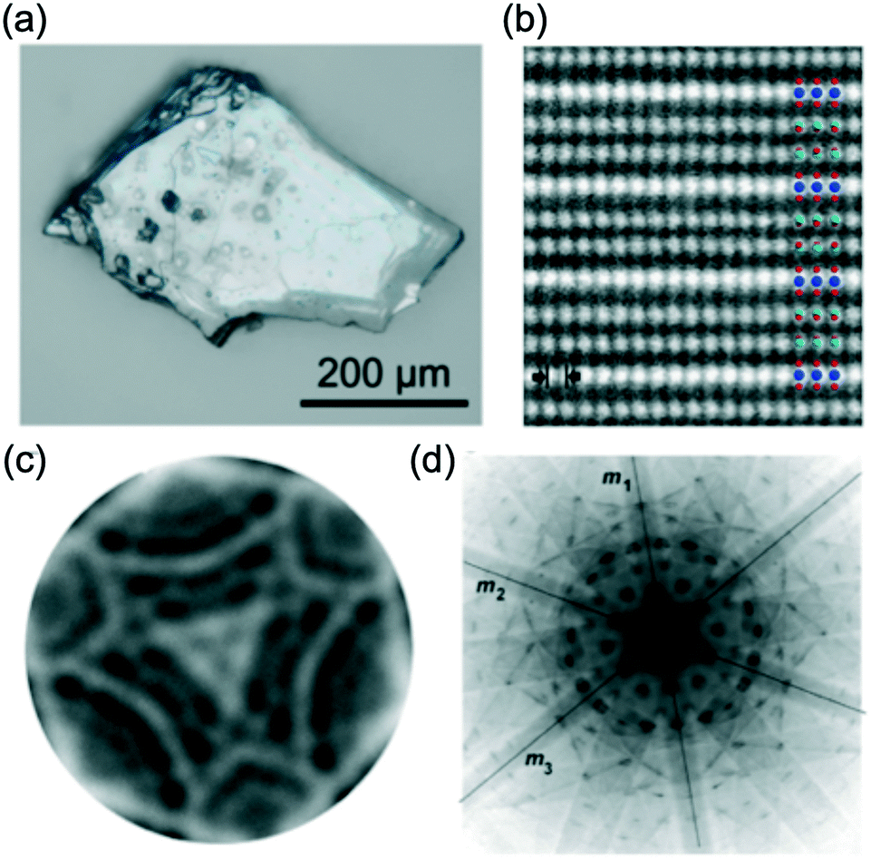 | ||
| Fig. 4 (a) Optical micrograph image of a single crystal of InGaO3(ZnO)1. (b) HAADF image of InGaZnO4 in [100] orientation with structure model. The blue, red, and light green circles represent In, Zn/Ga, and O atoms, respectively. Cation columns of In (bright) and Zn/Ga (medium bright) are well resolved indicating the cation layer stacking in InGaZnO4. A spacing of 0.16495 nm of the (20) prism planes is shown. (c) Central CBED disc and (d) whole pattern results suggest 3m symmetry. Panels (a–d) are reprinted with permission from ref. 46. © 2014 Elsevier. | ||
Convergent beam electron diffraction (CBED) was useful to determine the space group, because the whole crystal contributes to the diffraction pattern. The CBED patterns along the c-axis show a three-fold symmetry for the entire pattern (Fig. 4(d)) as well as for the central CBED disc (Fig. 4(c)). Analysis of the results suggested a trigonal crystal system with 3m symmetry, although the results of CBED yield two possible space groups: R3m and Rm.47 However, the six-fold symmetry of the diffraction pattern of the zero order Laue zone (ZOLZ) yields only the space group Rm.
The cell parameters at room temperature were determined by refining powder XRD data (a = 0.3284(3) nm and c = 2.6037(3) nm).46 The transparent crystals had a bluish-gray color and exhibited an excess of Ga expressed by the cation ratio of In:Ga:Zn = 30.2(9):39(1):31(1) at% as determined by energy dispersive X-ray spectroscopy (EDXS).46 This ratio indicated that the composition of the single crystal did not correspond to the ideal value, and that the quality of the crystal was poor. In addition, the aliovalent substitution of Zn by Ga was observed for the first time in the InGaO3(ZnO)n compounds. The chemical composition of the crystals was determined as (In0.9Ga0.1)Ga1.06Zn0.91□0.03O4 which is indicative of aliovalent substitution of Zn2+ by Ga3+ leading to vacancies in the cation sublattice due to the synthesis conditions. While the isovalent substitution of In3+ by Ga3+ is known, this is the first report of an aliovalent substitution of Zn2+ by Ga3+ in a member of the homologous series InGaO3(ZnO)n. This resulted in the formula (In0.9Ga0.1)Ga1.06Zn0.91□0.03O4 where 3% of the cations in 4 + 1 coordination are vacant due to aliovalent substitution. Thus, the depletion of Zn-ions was also found for the first time in a member of the homologous series InGaO3(ZnO)n.
Further evidence of the defect structure was found by considering the shortened a-axis (the c-axis does not change).16,19 Clearly, 6% of the Zn sites were substituted with the smaller Ga3+ ions (r(Ga3+) = 0.047 nm vs. r(Zn2+) = 0.06 nm in fourfold coordination) and with 3% vacant sites, there was clearly an effect on the lattice parameters when compared to InGaZnO4. If the oxygen ions were already in contact along the c-axis, there would not be an effect observed. However, if smaller ions and vacant sites were introduced into the wurtzite-type layer in InGaZnO4 the oxygen ion distance in the basal plane would be reduced. This results in a reduction in the length of the a-axis, which is exactly as observed in the XRD data.
 | ||
| Fig. 5 Crystal structure of InGaO3(ZnO)1. Coordination of InO6 is octahedra and Zn/GaO5 is trigonal bipyramid. Because Zn and Ga cannot be separated, the Zn/Ga mixed site is referred to as the trigonal bipyramid in this paper. | ||
Two layers of Zn and Ga ions sharing the same site with the composition ZnGaO2+ were found between the InO6 octahedral layers. Although the Zn/Ga mix site can be expressed as two layers of tetrahedra (trigonal bipyramid with off-center cations), in this article, the Zn/Ga mixed site is referred to as the trigonal bipyramid as shown in Fig. 5. Free refinement modeling made it difficult to determine the occupation factor of the isoelectronic Ga3+ and Zn2+ ions, so the factor was set to 0.5 to maintain charge neutrality. Zn and Ga showed trigonal bipyramidal 4 + 1 coordination with O ions; however, the cations were significantly displaced from the equatorial plane. Hence, InGaZnO4 (= InGaO3(ZnO)1) as the first member of the InGaO3(ZnO)n (n = integer) family has the same structural characteristics as other known members of homologous compounds.
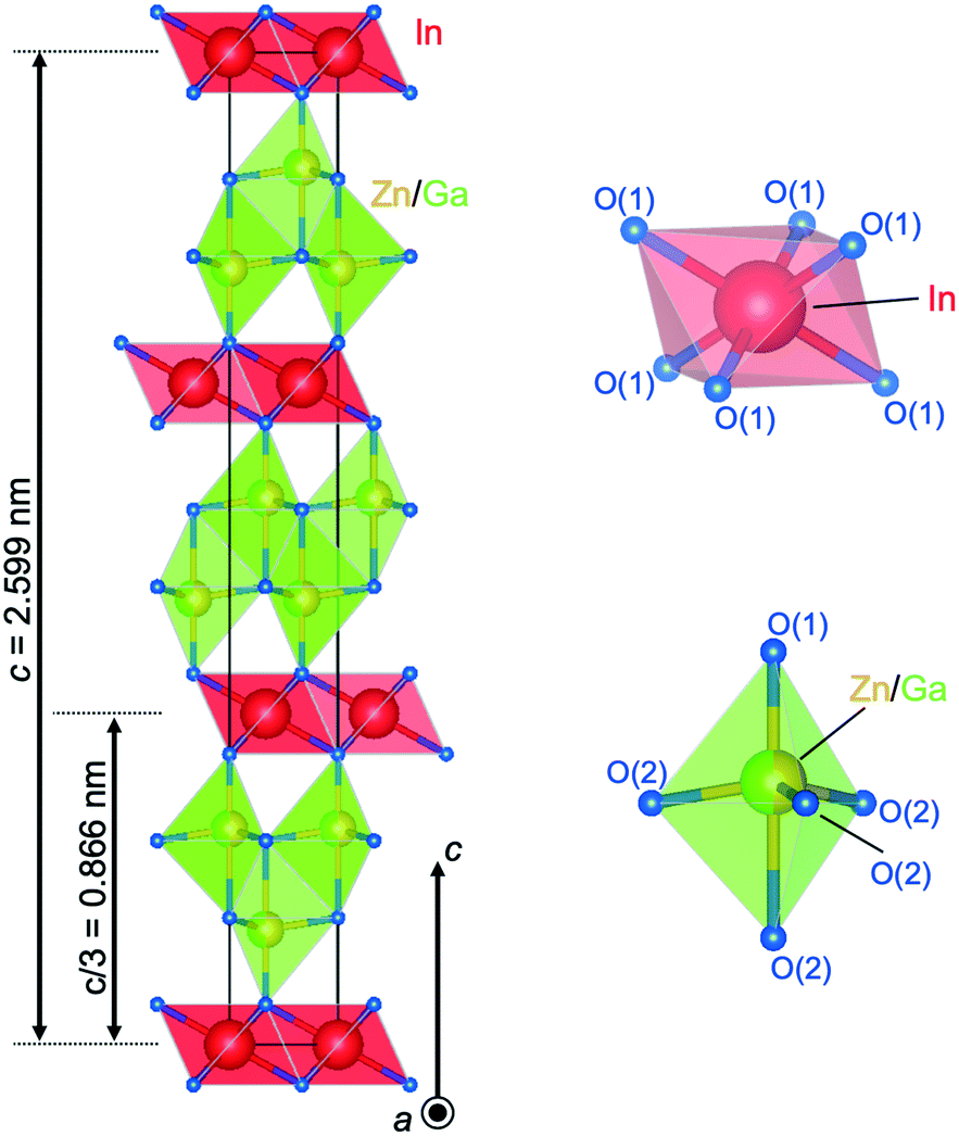
Structural data of LuFeO3(ZnO)3 were used as a starting model for the Rietveld refinement.26 The analysis revealed that IGZO-13 crystallized as the trigonal space group (Rm; no. 166) with parameters (a = 0.32871(9) nm; c = 4.1589(1) nm, Z = 3, reflection intensity-based reliability factor RBragg = 0.0506).48 The structural model was validated by bond valence calculations of the Ga3+ distribution.27 These calculations indicated a model with Ga3+ only in the trigonal bipyramid at the inversion plane within the wurtzite region. Thus, these trigonal bipyramids are statistically occupied by alternating Zn and Ga, while the tetrahedra linked to the layers of InO6 octahedra are occupied by Zn only.
Fig. 6 shows the crystal structure of IGZO-13. The inversion plane in the center of the ZnO4 region lies between two (Zn/Ga)O5 trigonal bipyramids. In the GaO5 trigonal bipyramid, the difference in the distances from Ga to the apical O(2) ions was a result of the position of Ga in the equatorial triangle of the trigonal bipyramid, which is slightly off-center in the c-axis direction. As distance increased from the InO6 octahedral layer, the Zn2+ ion in the ZnO4 tetrahedron shifted along the c-axis towards the center of the trigonal bipyramid. The distance between the cation and the apical oxygen increased from 0.18981 nm for Zn(1)–O(1) to 0.20395 for (Zn(2)/Ga(2))–O(2) and the distance to the basal oxygen decreased.
 | ||
| Fig. 6 Crystal structure of InGaO3(ZnO)3. Coordination of InO6 is octahedra, Zn(1)O4 is tetrahedra, and Zn(2)/GaO5 is trigonal bipyramid. | ||
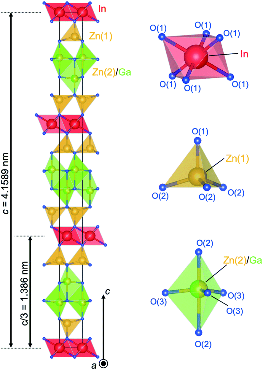
3.2 Small single crystal of IGZO-12 and IGZO-14
In this section, we introduce the small single crystals of the InGaO3(ZnO)n homologous series where n is even (n = 2, 4). One key feature of the analysis of the crystals is that the Zn and Ga sites are perfectly separated into ZnO4 tetrahedra and GaO5 trigonal bipyramids.:20 by weight. The platinum crucible was heated in a sealed platinum tube to 1623 K (1350 °C) for 5 days then cooled at a rate of 0.1 K min−1 to 873 K (600 °C). The single crystals obtained were removed from the K2MoO4-flux by washing with distilled water at 343 K (70 °C). The IGZO-12 crystals were colorless and the IGZO-14 were yellow.
Fig. 7(a and d) show the SEM images of single crystals of IGZO-12 and -14. The crystals are very small (less than 0.1 mm) and are smaller than the IGZO-11 crystals grown by the slow-cooling method.46 The shape of the single crystal indicates a hexagonal lattice. The chemical composition was determined by EDXS to be the ratio of In:Ga:Zn = 25.55:24.38:50.07 for IGZO-12 (ref. 48) and In:Ga:Zn = 17.83:16.37:65.80 for IGZO-14 (ref. 49) in at% with an error less than ±1 each. Both ratios are in close agreement with the ideal values. Based on these results, it appears that the crystals with n = 2, 4 are easier to grow than those with n = 1, 3.
 | ||
| Fig. 7 (a) SEM image of single crystals of InGaO3(ZnO)2. (b and c) CBED pattern in the [0001] zone axis of InGaO3(ZnO)2. Whole pattern (b) and bright field CBED disc (c) both exhibit hexagonal symmetry. (d) SEM image of single crystals of InGaO3(ZnO)4. (e and f) CBED pattern in the [0001] zone axis of InGaO3(ZnO)4. 6mm whole pattern symmetry and 6mm bright field symmetry. Panels (a–f) are reprinted with permission from ref. 48 and 49. © 2009 and 2010 John Wiley and Sons, Inc. | ||
The CBED patterns in the [0001] zone axis (Fig. 7(b and c)) exhibit 6mm whole-pattern symmetry as well as 6mm symmetry in the bright field disc (Fig. 7(e and f)). According to Morniroli and Steeds, two hexagonal space groups of P63mc and P63/mmc are still possible candidates.47 The number of independent mirror planes decides the space group, i.e., 2mm or 2m point group symmetry, respectively. As a result of higher order Laue zone reflections53 being examined in the electron diffraction patterns, it was concluded that InGaO3(ZnO)2 and InGaO3(ZnO)4 crystallize in the space group P63/mmc (no. 194).
Fig. 8 shows the crystal structure of IGZO-12. The inversion plane was built by Ga3+ ions in trigonal bipyramidal coordination in the wurtzite-type block at half distance between the layers of InO6 octahedra. The GaO5 polyhedra share corners between each other and with neighboring ZnO4 units. The site occupation of the isoelectronic Zn2+ and Ga3+, which are indistinguishable by XRD was confirmed by valence sum calculations.27 These calculations showed reasonable values only for Zn at the tetrahedral site and Ga in the trigonal bipyramidal interstices. Thus, the structure of IGZO-12 from single-crystal data clearly shows an ordering of the R cation in ARO3(ZnO)n with Ga3+ which occupies the inversion boundary.
 | ||
| Fig. 8 Crystal structure of InGaO3(ZnO)2. Coordination of InO6 octahedra, ZnO4 tetrahedra, and GaO5 trigonal bipyramid. | ||
One of the differences between n = odd and even in InGaO3(ZnO)n structures is the Ga position, which was found to be present in the trigonal bipyramid. Although the Ga position is off-center in the c-axis direction in IGZO-11 and -13, the GaO5 trigonal bipyramid has the same distance between Ga and the apical O(2) ions of 0.21379(2) nm in IGZO-12, because the position of the Ga atom is in the equatorial triangle of the trigonal bipyramid. The Zn2+ ion is shifted off the center of the ZnO4 tetrahedron along c towards the trigonal bipyramid which increased the angle O(2)–Zn–O(2) with respect to O(1)–Zn–O(2). This change in the Zn position was found to be the same regardless of the value of n.
Fig. 9 shows the crystal structure of IGZO-14. The structure has Zn(2)O layers inserted between Zn(1)O layers and GaO5 layers in the IGZO-12 structure. At both sides, the InO6 layers are connected by corners with ZnO4 tetrahedra. The position of GaO5 in IGZO-14 is different, and it is located under the Zn(1) atom instead of under the In atom as in IGZO-12. This inversion plane is built by Ga3+ ions filling trigonal bipyramidal sites in the wurtzite-type blocks at half distance between the layers of InO6 octahedra. The position of the inversion is located at the center of the trigonal bipyramidal GaO5, in the equivalent position to IGZO-12.
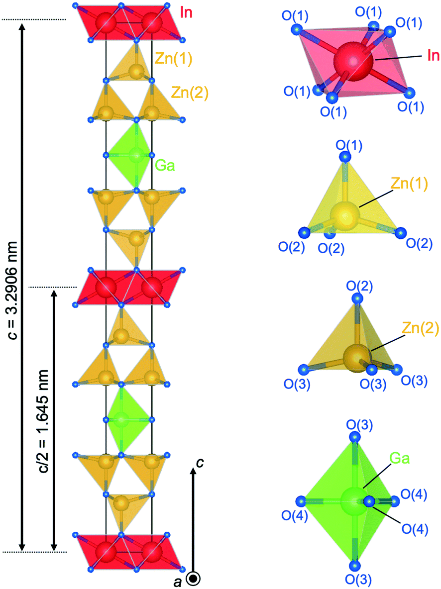 | ||
| Fig. 9 Crystal structure of InGaO3(ZnO)4. Coordination of InO6 octahedra, Zn(1)O4 tetrahedra, Zn(2)O4 tetrahedra, and GaO5 trigonal bipyramid. | ||
As mentioned before, the cations are shifted from the tetrahedron center towards the basal plane with increasing distance from the InO6 octahedral layer. The tendency was most clearly found in the IGZO-14 structure. The Zn2+ ion is shifted off the center of the ZnO4 tetrahedron along c-axis towards the oxygen triangle on the basal plane. The distance from Zn in the tetrahedron to the apex oxygen increased with increasing distance from the InO6 octahedral layer. The Zn(1)–O(1) distance was found to be 0.1955(9) nm, and Zn(2)–O(2) was 0.2038(9) nm. The Zn(2) site, which is farther from InO2, had a longer distance from the apex oxygen, which indicated that Zn(2) is closer to the basal plane. The GaO5 at an equal distance from the InO6 octahedra is in the equatorial triangle of the trigonal bipyramid without the Ga being shifting from the center as in other homologues.
The displacement parameters of O(4) showed that the oxygen ion in the equatorial plane of the GaO5 unit are elongated along c-axis. A comparison between the components with n = 2 and 4 showed an increasing displacement parameter of O(4). Although the result indicated a split position, attempts to refine this for the O(4) site showed no reasonable results. Similar results were not obtained for the single crystals of the homologous InGaO3(ZnO)n series. The reason for this significantly elongated displacement parameter along c-axis of the O(4) remains to be clarified.
The site occupation of Zn and Ga was determined by bond valence sum calculations,27 which is the same method as IGZO-12. The tetrahedra in the wurtzite-type region are increasingly deformed with decreasing distance to the InO6 octahedral layers. However, calculations taking into consideration the statistical distribution and replacement of Ga(1), Zn(1), and Zn(2) yielded less valid results. The calculation of the bond valence sum showed reasonable results only with Zn in tetrahedral sites and Ga in trigonal bipyramidal interstices. The crystal parameters of the InGaO3(ZnO)n (n = 1–4) single crystals are summarized in Table 1.
| IGZO-11 (ref. 45) | IGZO-11 (ref. 46) | IGZO-12 (ref. 48) | IGZO-13 (ref. 48) | IGZO-14 (ref. 49) | |
|---|---|---|---|---|---|
| Crystal group |
Rm (no. 166, Z = 3) |
Rm (no. 166, Z = 3) |
P63/mmc (no. 194, Z = 2) |
Rm (no. 166, Z = 3) |
P63/mmc (no. 194, Z = 2) |
| Lattice constants (nm) | a = 0.32990(2) | a = 0.3275(1) | a = 0.32909(2) | a = 0.328971(9) | a = 0.32850(2) |
| c = 2.6101(3) | c = 2.599(1) | c = 2.2485(2) | c = 4.1589(1) | c = 3.2906(3) | |
| Cell volume V (nm3) | 0.24601(3) | 0.2414(3) | 0.21089(3) | 0.389788 | 0.30752(4) |
| Crystal color | Colorless | Bluish-gray | Colorless | Yellow | Yellow |
| Growth method | High pressure (2 GPa) | Slow cooling | K2MoO4 flux | K2MoO4 flux | K2MoO4 flux |
| Crystal size (mm) | Not shown | ∼0.2 | ∼0.2 | Not shown | ∼0.2 |
| In:Ga:Zn ratio |
Not shown | 30.2:39:31 |
25.6:24.4:50.1 |
Not shown | 17.8:16.4:65.8 |
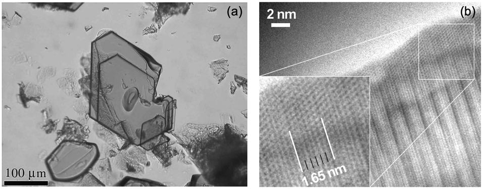 | ||
| Fig. 10 (a) Optical image of single crystals of InFeO3(ZnO)4. (b) HRTEM images of InFeO3(ZnO)4 imaged along <20> zone axis. Dark spot lines have the In-layer spacing of 1.65 nm. Panels (a and b) are reprinted with permission from ref. 54. © 2014 John Wiley and Sons, Inc. | ||
The structure of InFeO3(ZnO)4 was calculated as being in space group P63/mmc; no. 194 (a = 0.3211(6) nm; c = 3.3032(6) nm, Z = 2, R1 = 0.0368, wR2 = 0.0928)54 from XRD data. Alternating stacks of edge-sharing InO6 octahedra and 5 layers of corner-sharing (Zn/Fe)O4 tetrahedra were found. The composition was measured by EDXS and resulted in a ratio In:Fe:Zn equal to 18.3:16:65.7.54 The ratio indicated that the Fe value was slightly low, and that the ratio of IGZO-14 was closer to the ideal value. As shown in Fig. 10(b), a HRTEM image in <20> orientation is observed in InFeO3(ZnO)4. The In layers are seen as parallel contrasting dark lines with a spacing of c/2 = 1.65 nm and 5 lines generated from the 5 layers of Zn/Fe cations are also easily observed.
Refining the site occupation factors of the cations in (Zn/Fe)O4 tetrahedra resulted in a clear and reasonable gradient for the distribution of Fe. The site occupation factor refinement results for the highest Fe amount (34%) showed Fe on the trigonal bipyramidal position Zn(4)/Fe(4) and a gradual decrease from 23.2% with Zn(3)/Fe(3) to 9% with Zn(2)/Fe(2) towards the InO6 layers (the Zn(x)/Fe(x) sites are surrounded by the same x of the basal plane O(x) ion as shown in Fig. 9). Since the distribution of Fe was observed, it is desirable to consider a method that can directly observe the ratio of Ga/Zn ratio even in IGZO.
4 Single crystal growth by an optical floating zone method
In 2019, our group succeeded in growing large and high-quality single crystals of IGZO-11 using a novel and reproducible method.55 Using this process, we also succeeded in growing very small single crystals of IGZO-21.46 In this section, we introduce this growth method and the resulting bulk single crystals of IGZO-11 and tiny crystal of IGZO-21.4.1 Large single crystal of IGZO-11
The IGZO-11 crystals were successfully grown for the first time by the OFZ (optical floating zone) method in applying a gas pressure using a feed rod with a Zn-rich composition.55 A stable liquid phase was visually apparent at a pressure of ∼0.9 MPa. In addition, it was found that IGZO-11 melts at about 1923 K (1650 °C).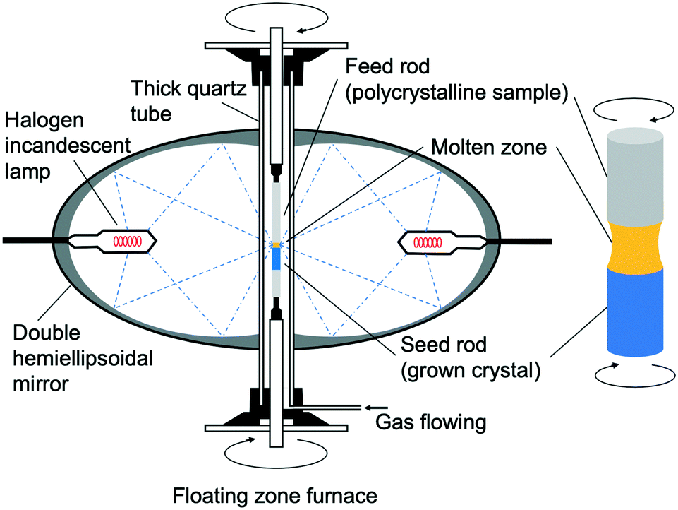 | ||
| Fig. 11 Schematic image of a floating zone furnace and crystal growth. | ||
The feed rods were prepared by a standard solid-phase reaction method using high purity reactants. Powders of In2O3 (99.99%, Furuuchi Chem.), Ga2O3 (99.99%, Furuuchi Chem.) and ZnO (99.99%, Kojundo Chem. Lab.) were preheated at 1523 K (1250 °C) in air for 24 hours. Using a molar ratio of 1:1:2 + x (0 < x < 0.2) of In2O3:Ga2O3:ZnO, the powders were weighed and thoroughly mixed in an agate mortar with ethanol. After drying, the mixtures were further ground, calcined at 1523 K (1250 °C) for 48 hours, then the calcined mixtures were thoroughly re-ground. The re-ground powders were densely packed in a rubber tube with a diameter of 6 mm and then evacuated using a rotary pump to improve both density and uniformity. The tube was then hydrostatically pressed at a pressure of 18 MPa. The polycrystalline rod was sintered at 1523 K (1250 °C) for 24 hours in air and was also used as the support rod (Fig. 12(a)). Single crystals of In–Ga–Zn–O were grown at a growth rate of 1.9 mm h−1 and gap speed of 2.0 mm h−1 in constantly flowing dry-air with a pressure of 0.1–0.9 MPa. The upper and lower polycrystalline rods were rotated in opposite directions at a rate of 16and 14 rpm, respectively. The rod-rotation speed may have been too slow, as the sample that was grown had a large variation in electrical conductivity.
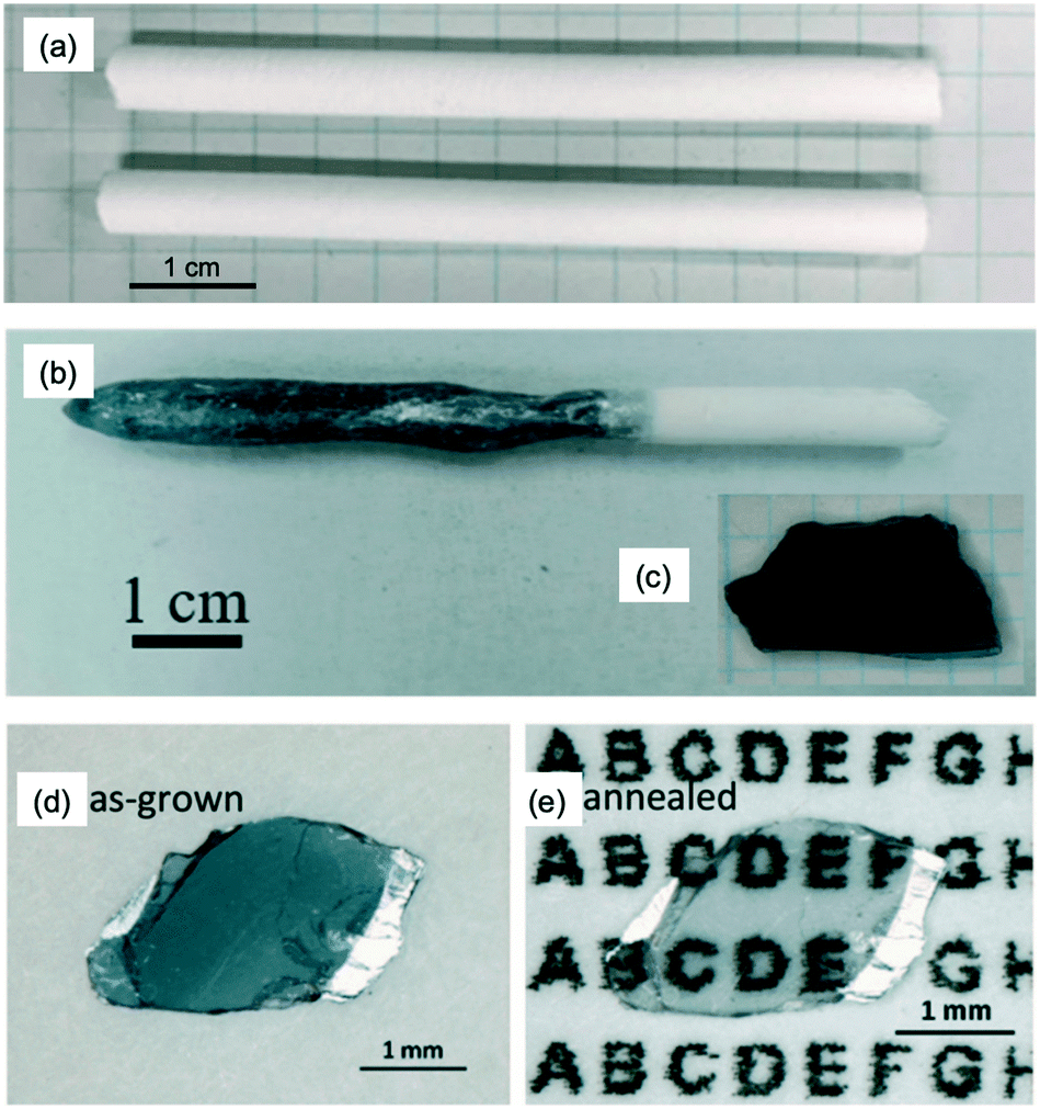 | ||
| Fig. 12 (a) Sintered polycrystalline rod of InGaO3(ZnO)1. (b) Rod-shaped InGaO3(ZnO)1 crystal grown by the OFZ method under a pressure of 0.9 MPa. (c) Plate-shaped single crystal, that was cleaved mechanically from the rod-shaped crystal, where the cleavage plane was perpendicular to the c-axis. (d) Image of the crystal without modification. (e) Image of the post-annealed crystal (1273 K (1000 °C) for 72 hours under a flow O2 gas at 0.1 MPa). Panels (b–d) are reprinted with permission from ref. 55. © 2019 Royal Society of Chemistry. | ||
In the growing process, a vaporized material (mainly ZnO) was found in the molten zone and deposited on the quartz tube located in the infrared radiation furnace. Suppression of the ZnO vaporization was found to be important in attaining a stable liquid phase in the molten zone and thus precipitating IGZO-11 as the primary phase. Thus, the two methods that were followed were: (i) synthesis was carried out in a pressurized atmosphere of P = 0.1–0.9 MPa under dry-air flow, and (ii) continuous supply of ZnO was provided using a feed rod with a Zn-rich composition during crystal growth.
The optimal growth conditions were found to be when the crystal growth was performed under pressures of 0.1, 0.6 and 0.9 MPa for feed rods with a stoichiometric ratio (In:Ga:Zn = 1:1:1) or pressures of 0.8 and 0.9 MPa for feed rods with a Zn-rich starting mixture (In:Ga:Zn = 1:1:1.1). The presence of IGZO-21 impurities was detected by the powder XRD patterns post synthesis. We found that the XRD peak-intensity of IGZO-21 decreased with increasing gas pressure and/or using a feed rod with a Zn-rich composition. This demonstrated that applying gas pressures of ≤0.9 MPa were very effective at reducing ZnO vaporization, but that these conditions did not suppress it completely. Thus, excess ZnO in the ratio was necessary to compensate for the loss of the ZnO due to vaporization.
As the evaporation of ZnO was observed during the crystal growth, it was likely that the crystals have Zn defects. In the sample grown at a low-gas pressure where the vaporization of ZnO was not suppressed, IGZO-21 crystals were obtained as primary products together with IGZO-11 crystals containing many Zn defects. On the other hand, samples prepared in combination with Zn-rich solutions under a pressure of P > 0.8 MPa had only a small amount of Zn vacancies. In addition, there were no IGZO-21 impurities in the crystals grown by under these optimum conditions.
X-ray fluorescence (XRF) spectra showed the defected areas and allowed the composition ratio of the crystals to be measured. The XRF spectra of the crystal shows the ratio of In:Ga:Zn = 0.95:1.00:0.94 in at%.55 The result indicated that the amount of cation defects is very small, which is consistent with the lattice constant, and indicates that a high quality crystal was produced. In addition, the chemical composition ratio was nearer to the stoichiometric ratio than that obtained from slow cooling in the Pt crucible,46 which indicates that the crystal is of higher quality. The crystal parameters of the large single crystal of IGZO-11 are summarized in Table 2.
| IGZO-11 (ref. 55) | IGZO-21 (ref. 68) | |
|---|---|---|
| Crystal group |
Rm (no. 166, Z = 3) |
P63/mmc (no. 166, Z = 4) |
| Lattice constants (nm) | a = 0.32990(4) | a = 0.33137(1) |
| c = 2.6018(3) | c = 2.9523(1) | |
| Cell volume V (nm3) | 0.24523 | 0.280748 |
| Crystal color | Bluish | Bluish |
| Growth method | Floating zone | Floating zone |
| Crystal size (mm) | ∼30 | ∼0.5 |
| In:Ga:Zn ratio |
0.95:1.00:0.94 |
19.9:59.9:20.2 |
| Air pressure (MPa) | 0.9 | 0.1 |
Single crystals with a size of 3–5 mm were annealed at 1273 K (1000 °C) for 72 hours under an oxygen pressure of 0.1 MPa. The heat treatment brought about a change in color of the crystals from blue to colorless. Fig. 12(d and e) show images of a single crystal before and after the annealing process. This result suggested that the color change may be caused by oxygen filling oxygen-deficient sites during the O2 annealing process. This color-change also indicates that the oxygen vacancies caused a change in the valence state of the three cations (In, Ga, Zn); however, which specific cation is affected is not yet clear.
To investigate the optical properties and determine the origin of the color-change, transmittance spectral data were collected, as shown in Fig. 13(a). An almost linear decrease was observed from 3.27 to 3.02 eV when n increased from 1 to 9,56 which was consistent with the decrease also observed for n = 1 to n = 3.16 Furthermore, when UV-visible spectra were recorded from one of the bluish single crystals, the spectra showed a substantial increase in remission in the UV region. This corresponded to the optical band gap, which was determined to be Eg = 3.17 eV by Tauc plot.57–59 This optical gap is slightly smaller than the band gap Eg = 3.27 eV of InGaO3(ZnO) that was determined by our group.55 The energy gap value is plotted in Fig. 13(c), as InGaO3(ZnO)0.5. The value is a large deviation from that found in InGaO3(ZnO)n.
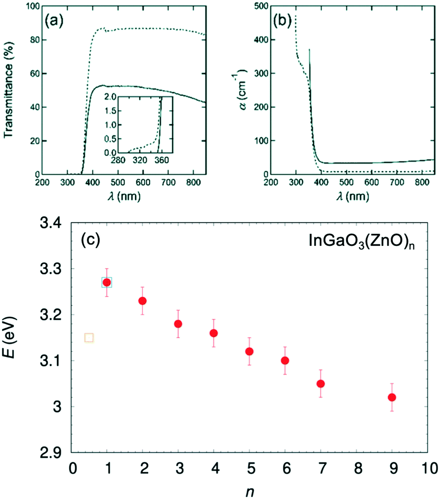 | ||
| Fig. 13 (a) The transmission spectra of single crystal IGZO-11 before (solid line) and after (dotted line) the O2 annealing at 1273 K (1000 °C) in 72 hours. The inset is an enlargement of the region of shorter incident photon wavelength. The sample thickness is 0.195 mm. (b) The adsorption coefficient α vs. wavelength of the incident photon λ for an unmodified, and the post-annealed, single crystal. (c) Evolution of the band gap in the series InGaO3(ZnO)n estimated using a Tauc plot. Circle symbol represents the gap values estimated from the polycrystalline sample56 and square symbols55,68 estimated from single crystals. Panels (a and b) are reprinted with permission from ref. 55. © 2019 Royal Society of Chemistry. | ||
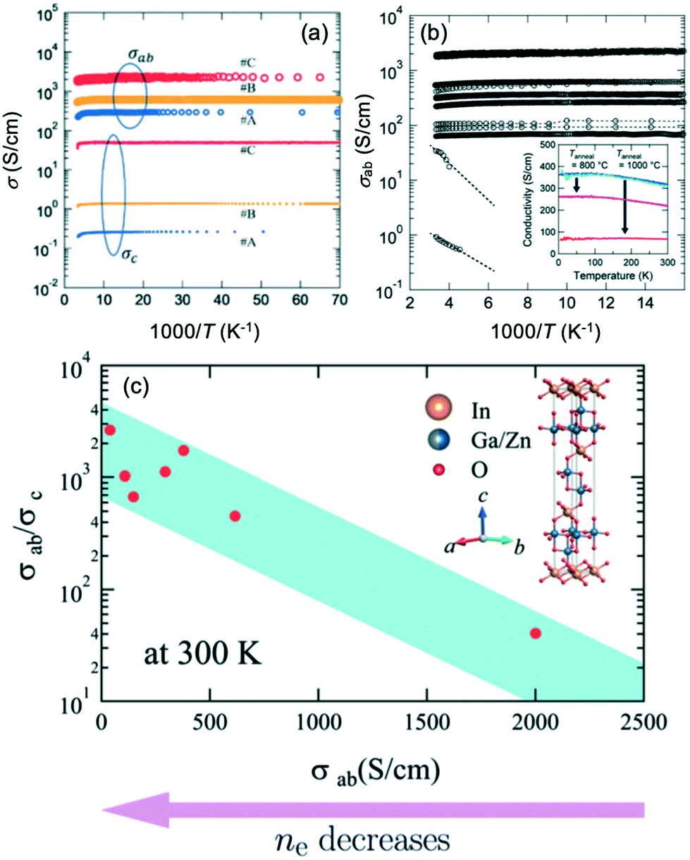 | ||
| Fig. 14 (a) Comparison of electrical conductivities for in-plane (σab) and out-of-plane (σc) unmodified IGZO-11 single crystals. (b) Arrhenius plots of the in-plane electrical conductivity σab(T), inset of (b) shows that the annealing temperature effect of the σab of IGZO-11, where the T anneal for purple and red circles are 1073 K (800 °C) and 1273 K (1000 °C), respectively, and the annealing time for both samples was fixed at 10 hours. (c) The anisotropic ratio σab/σc for single crystals at 300 K. Panels (a–c) are reprinted with permission from ref. 55. © 2019 Royal Society of Chemistry. | ||
Fig. 15(a and b) show the Arrhenius plots of the carrier density ne(T) and the Hall mobility μe(T) for bulk IGZO-11 single crystals. The increase in the Hall mobility with increasing carrier density is the opposite of the standard behavior of single crystal semiconductors such as β-Ga2O3.61–63 Confirmation of these anomalous properties in bulk single crystals is important to understand whether this phenomenon is intrinsic in IGZO systems. Fig. 15(c) shows μe(300 K) of bulk single crystals of IGZO-11 plotted as a function of ne(300 K) including a-IGZO,2,64 sc-IGZO-1n,39,65 poly-crystalline IGZO (pc-IGZO).6
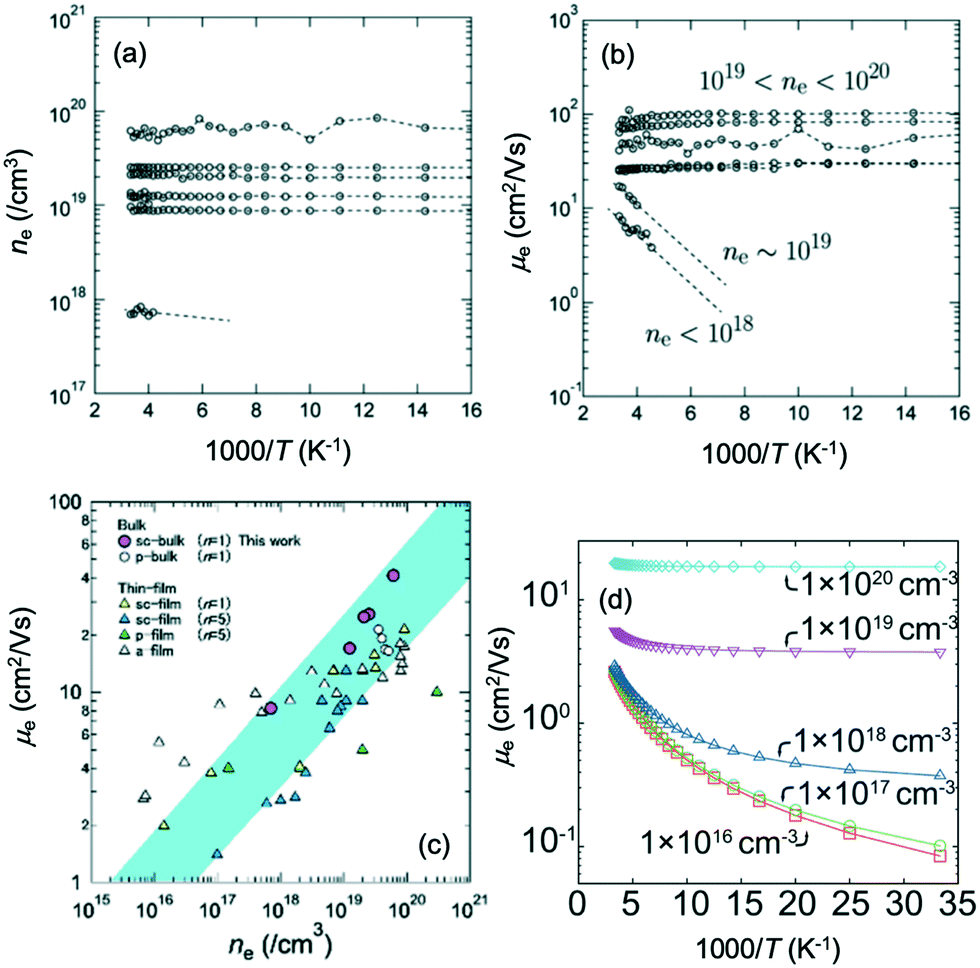 | ||
| Fig. 15 Arrhenius plots of (a) the carrier density ne(T) and (b) the Hall mobility μe(T) for bulk IGZO-11 single crystals. (c) The carrier density dependence of the Hall mobility at 300 K for bulk IGZO-11 single crystals (purple circles). Hall mobilities μe(ne) of bulk IGZO-11 single crystals are compared to those of a-IGZO, sc-IGZO-1n, pc-IGZO-11. (d) Theoretical calculation of the temperature dependence of Hall mobility at various carrier densities. Panels (a–c) are reprinted with permission from ref. 55. © 2019 Royal Society of Chemistry. Panel (d) is reprinted with permission from ref. 66. © 2013 AIP Publishing LLC. | ||
The relationship between μe(300 K) and ne(300 K) is typical for the thermally activated conductivity observed in amorphous semiconductors, our bulk single crystals also exhibited the same behavior, which is unusual. However, the Hall mobility of the bulk single crystals was larger than those of the other reported sample,2,6,39,64,65 when ne(300 K) exceeds 1019 cm−3. The reason for this difference was attributed to the decrease in relaxation time due to disorders such as grain boundaries and anti-site defects in the InO2 conducting layer. Based on these characteristics, we believe that it is worth investigating possible device applications using IGZO bulk single crystals.
Fig. 15(d) shows the calculated Arrhenius plots of the Hall mobility μe(T).66 In the model, cation-disorder scattering, ionized impurity, and polar optical phonon scattering66,67 were considered. The calculated mobility values accurately reproduced the temperature dependence of the mobility reported in both conventional thin film and amorphous systems. Relaxation time of cation-disorder scattering increased rapidly at low electron energies and this was seen as the main reason the mobility increased with increasing carrier density. However, there was a difference of an order of magnitude in our measurement results, which indicated that more accurate parameters are required in future studies.
4.2 Small single crystal of IGZO-21
As mentioned previously, we discovered a (InGaO3)2ZnO phase (or InGaO3(ZnO)0.5, IGZO-21) in the process of growing the IGZO-11 crystal by the OFZ method. The crystal structure is another homologues type, and has a structure in which m is changed in (InGaO3)mZnO. The homologues compounds with only m = 1 and 2 have been reported.:Ga:Zn = 1:1:1). The crystal bar was grown in constant gas flow of dry air in a pressure region of 0.1 MPa where Zn easily evaporates due to insufficient pressurization. We note that the conditions were not optimal for the crystal growth of IGZO-21 and further optimization is required.
:Ga:Zn = 19.87:59.88:20.24 in at% with an error of ±1.4 at%.68 Thus, the cation ratio was assigned to the chemical formula In1−xGa1+xO3(ZnO)0.5. Consequently, in crystals of the averaged composition, the octahedral site is occupied with In and Ga in a ratio of In:Ga = 0.5:0.5 resulting in octahedral (In0.5Ga0.5)O6 and trigonal bipyramidal (Ga1.0)O5 arrangements. The wide range in the chemical ratio at each crystal may have originated from the method of growth. In the OFZ method, the temperature gradient from the center axis of the rod to the surface led to evaporation of volatile oxides preferentially at the surface where there was also a loss of In2O3.
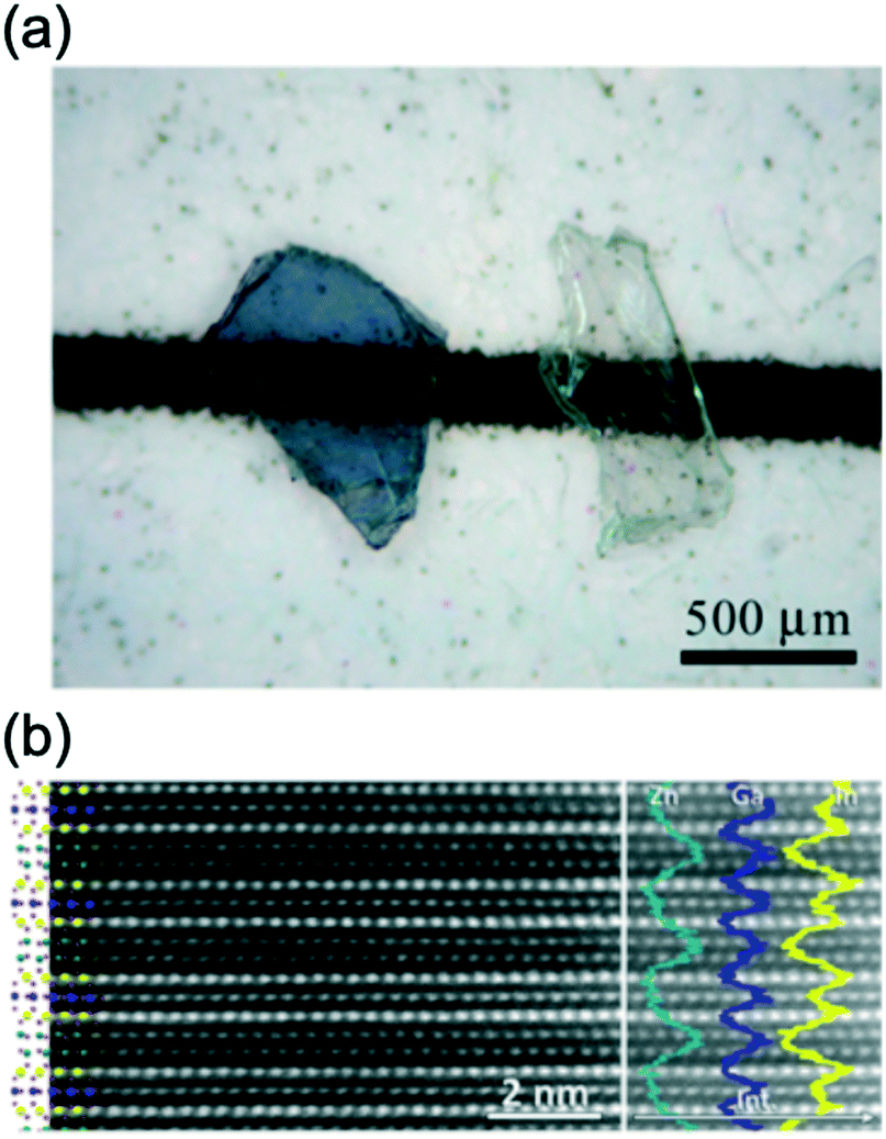 | ||
| Fig. 16 (a) Single crystals of In1−xGa1+xO3(ZnO)0.5 before (left) and after annealing (right). (b) HAADF image with crystal structure of (InGaO3)2ZnO overlayed (left) and extracted EDX line-scan profiles for In–L (yellow), Ga–K (blue) and Zn–K (cyan) as overlay (right). Panels (a and b) are reprinted with permission from ref. 68. © 2020 Elsevier. | ||
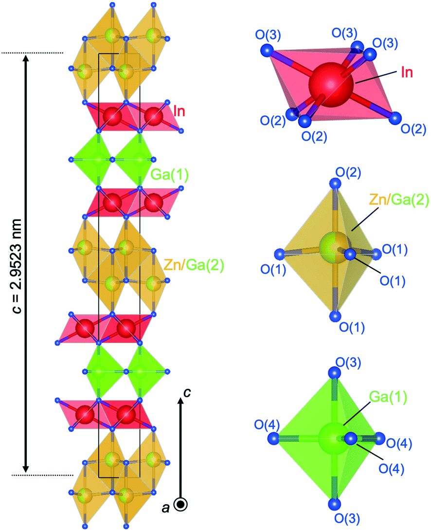 | ||
| Fig. 17 Crystal structure of (InGaO3)2ZnO. Coordination of InO6 is octahedra, Zn/Ga(2)O5 trigonal bipyramids (two Zn/Ga(2)O4 tetrahedra), and Ga(1)O5 trigonal bipyramid. | ||
Distinguish Ga3+ and Zn2+ by using XRD is difficult. 71Ga NMR and EXAFS revealed that Ga also occupied the octahedral sites found for InGaO3(ZnO)1.70 Mixed occupation of Ga and Zn in the two layers of tetrahedra was also demonstrated. The distribution of the cations on the octahedral, trigonal-bipyramidal and tetrahedral sites was made in concordance with the results of HRTEM. Fig. 16(b) shows a HAADF image with well-resolved cation columns in the structure model derived from single crystal XRD (left) and extracted EDX line-scan profiles (right) (In–L (yellow), Ga–K (blue) and Zn–K (cyan) as overlay). The layer stacking of these blocks is seen in Fig. 16(b). The GaO5 trigonal bipyramid is sandwiched between InO6 layers. Two Zn/Ga(2)O4 tetrahedra were also found to be sandwiched between InO6 layers.
A refinement of the single crystal data with a mixed occupation of the octahedral site by In and Ga led to a slight improvement of the R-values and to an occupation of the octahedra with 91%-In and 9%-Ga. All distances and angles in (InGaO3)2ZnO agreed with previously reported distances and angles from XRD data for InGaO3(ZnO)n compounds with n = 1, 2, 3 and 4 (ref. 46, 48, 49 and 68) and the only exception was the Ga(2) coordination. The Ga atom in the wurtzite slabs shows a close to ideal trigonal bipyramid and is in the center of the trigonal O(4) plane with distances of 0.191317(6) nm to the O(4) plane and 0.1999(3) nm to the apical O(3) site. The site symmetry of Ga in the wurtzite slabs in InGaO3(ZnO)n with n = 2, 4 also gave ideal angles for a trigonal bipyramid. However, the distances to the apical oxygen positions were elongated to 0.215 nm, while the Ga–O distances of 0.191 nm in the trigonal plane are the similar to those in (InGaO3)2ZnO.
To determine the cation distribution at the individual polyhedral layers of (InGaO3)2ZnO, high resolution SEM and TEM studies were conducted as shown in Fig. 16(b). Because of the dependence of intensity on the atomic number Z′, the In cations (Z′ = 49) are the brightest HAADF signal. However, the layers of Ga between the two layers of InO6 appear more intensely than the pair of Ga/Zn layers. This could be explained by “crosstalk” with the adjacent In atoms and/or by the shape of the electron probe. EDX analysis and the findings of Narendranath et al.,70 meant that we could not exclude the idea that Ga partially occupies the octahedral layers. Additionally, atomic resolution imaging in the electron microscope suggested a perfect periodic stacking of the atomic layers.
5 Conclusion
We introduced the recent advances in growing single crystals of the homologous (InGaO3)m(ZnO)n series. The detailed crystal structures were determined for (InGaO3)m(ZnO)n (n = 1–4). Large single crystals facilitate experiments that cannot be conducted by using polycrystalline or thin films. Our group declared that the OFZ method in applying air pressure is an efficient tool for growing large single crystals of IGZO We noted that excess ZnO is also essential, because the gas pressure is effective but not suppress ZnO vaporization completely.Furthermore, understanding the anisotropy of the electrical conductivity of InGaO3(ZnO)n is critical for clarifying the mechanism of the conductivity of the IGZO series. Large single crystals facilitate experimentation for determining the transport properties due to the structures of these compounds. Fig. 18 shows the length of the a-axis and c-axis/Z of InGaO3(ZnO)n. Because Z is the number of formula units in the structural unit cell, c/Z shows the In–In distance along the c-axis in InGaO3(ZnO)n (n ≥ 1). The length of the c-axis in the InGaO3(ZnO)n series is expressed by c/Z = 6.060 + 2.598 × n.17 The length determined for the single crystals was in good agreement with that of the polycrystalline sample. When In-5s mainly contributes to the electrical conductivity owing to an increasing distance of In–In layers with increasing n, we can predict that the conductivity along the c-axis becomes worse. In addition, IGZO-21 may have less anisotropy than IGZO-11 because it has a short average In–In distance. The relationship between the c-axis conductivity and the number of ZnO layers n remains to be clarified in experiments. To demonstrate the anisotropy, large single crystal growth of InGaO3(ZnO)n with larger n is necessary, and we are currently conducting these experiments.
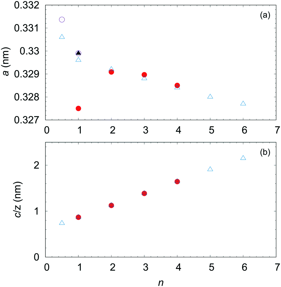 | ||
| Fig. 18 (a) Lattice parameter a and (b) layer width c/Z of homologous compounds InGaO3(ZnO)n as function of n. Open triangle symbols represent lattice constants estimated from the polycrystalline sample.23 Solid triangles represent small single crystal obtained from high pressure (2 GPa).45 Open circle symbols represent estimates from single crystals grown by the OFZ method.55 Solid circles represent estimates from small single crystals.46,48,49 | ||
The analysis of neutron diffraction results could lead to an understanding of the distribution of Zn/Ga in the single crystals. As distinguishing between Zn2+ and Ga3+ by performing XRD is impossible, an experiment to directly observe the distribution should be conducted instead. With the large single crystals we grew, the crystal structure can be analyzed using neutron diffraction, to directly observe the distribution. Although the Ga and Zn sites of n = 2, 4 are completely separated in the analysis using XRD, more studies are required to confirm this result.
High-quality single crystals allow us to systematically evaluate the physical properties of the IGZO series, e.g., thermal properties (Seebeck coefficient, thermal conductivity and specific heat). The properties were measured using a polycrystalline sample and IGZO thin film along the c-axis,41,56,71,72 and not reported using the bulk single crystal. In addition, angle-resolved photoemission spectroscopy (ARPES) could be performed using our large single crystals. Using ARPES data, we may be able to determine both a detailed energy gap and the Fermi surface. These experiments are now in progress. As many different measurements can be performed on our large single crystals, rapid and significant progress is expected in the research on the IGZO series.
Conflicts of interest
There are no conflicts to declare.Acknowledgements
This work was supported by JSPS KAKENHI Grant Number JP20K05306 and JP21K04909. A part of this work is also supported by Tokyo University's Science Grant for Young or Female Researchers, the Grants for Young Researcher from JGC-S Scholarship Foundation, Iketani Science and Technology Foundation, and Murata Science Foundation. Crystal structures schematics were produced using VESTA.73References
- K. Nomura, H. Ohta, K. Ueda, T. Kamiya, M. Hirano and H. Hosono, Science, 2003, 300, 1269 CrossRef CAS PubMed.
- K. Nomura, H. Ohta, A. Takagi, T. Kamiya, M. Hirano and H. Hosono, Nature, 2004, 432, 488–492 CrossRef CAS PubMed.
- S. Amano, H. Harada, K. Akimoto, J. Sakata, T. Nishi, K. Moriya, K. Wakimoto, J. Koyama, S. Yamazaki, Y. Oikawa, T. Ikeyama and M. Sakakura, Dig. Tech. Pap. – Soc. Inf. Disp. Int. Symp., 2010, 41, 626 CrossRef CAS.
- T. Nishi, K. Moriya, S. Fukai, Y. Kubota, K. Akimoto, J. Sakata, K. Kusunoki, R. Arasawa, K. Wakimoto, J. Koyama, S. Yamazaki, Y. Oikawa, K. Okazaki and M. Sakakura, Dig. Tech. Pap. - Soc. Inf. Disp. Int. Symp., 2010, 41, 1685 CrossRef.
- K. Toyotaka, K. Kusunoki, T. Nagata, Y. Hirakata, K. Wakimoto, J. Koyama, S. Yamazaki, R. Sato, K. Okazaki and M. Sakakura, Jpn. J. Appl. Phys., 2011, 50, 03CC09 CrossRef.
- M. Orita, M. Takeuchi, H. Sakai and H. Tanji, Jpn. J. Appl. Phys., 1995, 34, L1550–L1552 CrossRef CAS.
- K. Kato, Y. Shionoiri, Y. Sekine, K. Furutani, T. Hatano, T. Aoki, M. Sasaki, H. Tomatsu, J. Koyama and S. Yamazaki, Jpn. J. Appl. Phys., 2012, 51, 021201 CrossRef.
- N. Yamada, R. Ino, H. Tomura, Y. Kondo and Y. Ninomiya, Adv. Electron. Mater., 2017, 3, 1700298 CrossRef.
- S. Yamazaki, J. Koyama, Y. Yamamoto and K. Okamoto, Dig. Tech. Pap. - Soc. Inf. Disp. Int. Symp., 2012, 43, 183–186 CrossRef CAS.
- S. Yamazaki, T. Hirohasi, M. Takahashi, S. Adachi, M. Tsubuku, J. Koezuka, K. Okazaki, Y. Kanzaki, H. Matsukizono, S. Kaneko, S. Mori and T. Matsuo, J. Soc. Inf. Disp., 2014, 22(1), 55–67 CrossRef CAS.
- K. Kato, Y. Shionoiri, Y. Sekine, K. Furutani, T. Hatano, T. Aoki, M. Sasaki, H. Tomatsu, J. Koyama and S. Yamazaki, Jpn. J. Appl. Phys., 2012, 51, 21201 CrossRef.
- Y. Sekine, K. Furutani, Y. Shionoiri, K. Kato, J. Koyama and S. Yamazaki, ECS Trans., 2011, 37, 77–88 CrossRef CAS.
- M. Tsubuku, D. Matsubayashi, T. Takeuchi, R. Honda, T. Murakawa, S. Matsuda, Y. Yamamoto and S. Yamazaki, ECS Trans., 2015, 67, 17–22 CrossRef CAS.
- Physics and Technology of Crystalline Oxide Semiconductor CAAC–IGZO: Application to Displays, ed. S. Yamazaki and T. Tsutsui, Wiley, U.K., 2017 Search PubMed.
- N. Kimizuka and T. Mohri, J. Solid State Chem., 1985, 60, 382–384 CrossRef CAS.
- T. Moriga, D. R. Kammler and T. O. Mason, J. Am. Ceram. Soc., 1999, 82, 2705–2710 CrossRef CAS.
- N. Kimizuka, M. Isobe and M. Nakamura, J. Solid State Chem., 1995, 116, 170–178 CrossRef CAS.
- C. Li, Y. Bando, M. Nakamura, M. Onoda and N. Kimizuka, J. Solid State Chem., 1998, 139, 347–355 CrossRef CAS.
- M. Nakamura, N. Kimizuka and T. Mohri, J. Solid State Chem., 1991, 93, 298–315 CrossRef CAS.
- N. Kimizuka, T. Mohri, Y. Matsui and K. Siratori, J. Solid State Chem., 1988, 74, 98–109 CrossRef CAS.
- M. Nakamura, N. Kimizuka and T. Mohri, J. Solid State Chem., 1989, 81, 70 CrossRef.
- J. Iida, S. Takekawa and N. Kimizuka, J. Cryst. Growth, 1990, 102, 398–400 CrossRef CAS.
- M. Nakamura, N. Kimizuka and T. Mohri, J. Solid State Chem., 1991, 93, 298–315 CrossRef CAS.
- N. Kimizuka, T. Mohri and Y. Matsui, J. Solid State Chem., 1988, 74, 98–109 CrossRef CAS.
- N. Kimizuka and E. Takayama, J. Solid State Chem., 1982, 41, 166–173 CrossRef CAS.
- M. Isobe, N. Kimizuka, M. Nakamura and T. Mohri, Acta Crystallogr., Sect. C: Cryst. Struct. Commun., 1994, 50, 332–336 CrossRef.
- S. Adams, Acta Crystallogr., Sect. B: Struct. Sci., 2001, 57(2001), 287 Search PubMed , http://kristall.unimki.gwdg.de/softbv/index.html.
- N. Kimizuka, A. Takenaka, Y. Sasada and T. Katsura, Solid State Commun., 1974, 15, 1199–1201 CrossRef CAS.
- K. Kato, I. Kawada, N. Kimizuka and T. Katsura, Z. Kristallogr., 1976, 143, 278–284 CAS.
- R. Grajczyk and M. A. Subramanian, Prog. Solid State Chem., 2015, 43, 37–46 CrossRef CAS.
- N. Kimizuka and E. Takayama, J. Solid State Chem., 1984, 53, 217–226 CrossRef CAS.
- F. Lappe, A. Niggli, R. Nitsche and J. White, Z. Kristallogr., Kristallgeom., Kristallphys., Kristallchem., 1962, 117, 146 CrossRef CAS.
- S. Yonezawa, T. Kajikawa and Y. Maeno, Phys. Rev. Lett., 2013, 110, 077003 CrossRef PubMed.
- S. Kittaka, Y. Aoki, Y. Shimura, T. Sakakibara, S. Seiro, C. Geibel, F. Steglich, H. Ikeda and K. Machida, Phys. Rev. Lett., 2014, 112, 067002 CrossRef PubMed.
- Y. Matsumoto and S. Nakatsuji, Rev. Sci. Instrum., 2018, 89, 033908 CrossRef PubMed.
- N. Kase, Y. Terui, T. Nakano and N. Takeda, Phys. Rev. B, 2017, 96, 214506 CrossRef.
- N. Kase, J. Phys. Soc. Jpn., 2019, 88, 041007 CrossRef.
- H. Ohta, K. Nomura, M. Orita, M. Hirano, K. Ueda, T. Suzuki, Y. Ikuhara and H. Hosono, Adv. Funct. Mater., 2003, 13, 1398 CrossRef.
- K. Nomura, T. Kamiya, H. Ohta, K. Ueda, M. Hirano and H. Hosono, Appl. Phys. Lett., 2004, 85, 1993 CrossRef CAS.
- H. Hosono, T. Kamiya and M. Hirano, Bull. Chem. Soc. Jpn., 2006, 79, 1–24 CrossRef CAS.
- H. J. Cho, Y. Wu, Y.-Q. Zhang, B. Feng, M. Mikami, W. Shin, Y. Ikuhara, Y.-M. Sheu, K. Saito and H. Ohta, Adv. Mater. Interfaces, 2021, 8, 2001932 CrossRef CAS.
- S. Yamazaki, H. Suzawa, K. Inoue, K. Kato, T. Hirohashi, K. Okazaki and N. Kimizuka, Jpn. J. Appl. Phys., 2014, 53, 04ED18 CrossRef.
- S. Yamazaki, S. Ohshita, M. Oota, H. Baba, T. Onuki, H. Kunitake, K. Ohshima, D. Shimada, H. Kimura, T. Murakawa, T. Atsumi and K. Kato, Int. J. Ceram. Eng. Sci., 2019, 1, 6–20 CrossRef.
- D. M. Lynch, B. Zhu, B. D. A. Levin, D. A. Muller, D. G. Ast, R. G. Greene and M. O. Thompson, Appl. Phys. Lett., 2014, 105, 262103 CrossRef.
- M. Nespolo, A. Sato, T. Osawa and H. Ohashi, Cryst. Res. Technol., 2000, 35, 151–165 CrossRef CAS.
- W. Assenmacher, G. Schnakenburg, Y. Michiue, Y. Kanke, N. Kimizuka and W. Mader, J. Solid State Chem., 2014, 215, 176–183 CrossRef CAS.
- J. P. Morniroli and J. W. Steeds, Ultramicroscopy, 1992, 45, 219 CrossRef CAS.
- I. Keller, W. Assenmacher, G. Schnakenburg and W. Mader, Z. Anorg. Allg. Chem., 2009, 635, 2065–2071 CrossRef CAS.
- I. Keller and W. Mader, Z. Anorg. Allg. Chem., 2010, 636, 1045–1049 CrossRef CAS.
- S. Eichhorn and W. Mader, J. Solid State Chem., 2016, 233, 75–81 CrossRef CAS.
- S. Eichhorn, H. Schmid, W. Assenmacher and W. Mader, J. Solid State Chem., 2017, 46, 214–220 CrossRef.
- J. Garling, W. Assenmacher, H. Schmid, P. Longo and W. Mader, J. Solid State Chem., 2018, 258, 809–817 CrossRef CAS.
- A. Magrez, J. P. Morniroli, M. Caldes, A. Marie, O. Joubert and L. Brohan, J. Solid State Chem., 2003, 172, 243 CrossRef CAS.
- S. Erichsen, W. Assenmacher, G. Schnakenburg and W. Mader, Z. Anorg. Allg. Chem., 2014, 640, 2817–2822 CrossRef CAS.
- Y. Tanaka, K. Wada, Y. Kobayashi, T. Fujii, S. J. Denholme, R. Sekine, N. Kase, N. Kimizuka and N. Miyakawa, CrystEngComm, 2019, 21, 2985 RSC.
- S. Préaud, C. Byl, F. Brisset and D. Berardan, J. Am. Ceram. Soc., 2020, 103, 3030–3038 CrossRef.
- J. Tauc, R. Grigovici and A. Vancu, Phys. Status Solidi, 1966, 15, 627 CrossRef CAS.
- B. D. Viezbicke, S. Patel, B. E. Davis and D. P. Birnie, Phys. Status Solidi B, 2015, 252, 1700–1710 CrossRef CAS.
- T. Kamiya, K. Nomura and H. Hosono, Phys. Status Solidi A, 2009, 206, 860–867 CrossRef CAS.
- M. Orita, H. Tanji, M. Mizuno, H. Adachi and I. Tanaka, Phys. Rev. B: Condens. Matter Mater. Phys., 2000, 61, 1811–1815 CrossRef CAS.
- H. H. Tippins, Phys. Rev. A, 1965, 140, A316 CrossRef.
- M. R. Lorenz, J. F. Woods and R. J. Gambino, J. Phys. Chem. Solids, 1967, 28, 403 CrossRef CAS.
- N. Ueda, H. Hosono, R. Waseda and H. Kawazoe, Appl. Phys. Lett., 1997, 70, 3561 CrossRef CAS.
- A. Takagia, K. Nomura, H. Ohta, H. Yanagi, T. Kamiya, M. Hirano and H. Hosono, Thin Solid Films, 2005, 486, 38–41 CrossRef.
- T. Kamiya, K. Nomura and H. Hosono, Sci. Technol. Adv. Mater., 2010, 11, 044305 CrossRef PubMed.
- Y. Kang, Y. Cho and S. Han, Appl. Phys. Lett., 2013, 102, 152104 CrossRef.
- B. K. Ridley, Quantum Process in Semiconductors, Oxford University Press, New York, 3rd edn, 1993 Search PubMed.
- D. Lahr, W. Assenmacher, H. Schmid, N. Kimizuka, A. Kamai, Y. Tanaka, N. Miyakawa and W. Mader, J. Solid State Chem., 2020, 288, 121341 CrossRef CAS.
- K. Kato, I. Kawada, N. Kimizuka and T. Katsura, Z. Kristallogr., 1975, 141, 314–320 CrossRef CAS.
- S. B. Narendranath, A. K. Yadav, T. G. Ajithkumar, D. Bhattacharyya, S. N. Jha, K. K. Dey, T. Raja and R. N. Devi, Dalton Trans., 2014, 43, 2120–2126 RSC.
- T. Yoshikawa, T. Yagi, N. Oka, J. Jia, Y. Yamashita, K. Hattori, Y. Seino, N. Taketoshi, T. Baba and Y. Shigesato, Appl. Phys. Express, 2013, 6, 021101 CrossRef.
- Y. Fujimoto, M. Uenuma, Y. Ishikawa and Y. Uraoka, J. Electron. Mater., 2016, 45, 1377–1381 CrossRef CAS.
- K. Momma and F. Izumi, J. Appl. Crystallogr., 2011, 44, 1272–1276 CrossRef CAS.
| This journal is © The Royal Society of Chemistry 2022 |