
 Open Access Article
 This Open Access Article is licensed under a Creative Commons Attribution-Non Commercial 3.0 Unported Licence
Liquid crystal elastomers as substrates for 3D, robust, implantable electronics†
Jimin
Maeng‡
a,
Rashed T.
Rihani‡
a,
Mahjabeen
Javed
a,
Jai Singh
Rajput
a,
Hyun
Kim§
a,
Ian G.
Bouton
b,
Tyler A.
Criss
b,
Joseph J.
Pancrazio
a,
Bryan J.
Black
a and
Taylor H.
Ware
 *a
*a
aDepartment of Bioengineering, University of Texas at Dallas, 800 W. Campbell Road, Richardson, TX 75080, USA. E-mail: taylor.ware@utdallas.edu
bQualia Inc., 17217 Waterview Parkway, Dallas, TX 75252, USA
First published on 15th April 2020
Abstract
New device architectures favorable for interaction with the soft and dynamic biological tissue are critical for the design of indwelling biosensors and neural interfaces. For the long-term use of such devices within the body, it is also critical that the component materials resist the physiological harsh mechanical and chemical conditions. Here, we describe the design and fabrication of mechanically and chemically robust 3D implantable electronics. This is achieved by using traditional photolithography to pattern electronics on liquid crystal elastomers (LCEs), a class of shape programmable materials. The chemical durability of LCE is evaluated under accelerated in vitro conditions simulating the physiological environment; for example, LCE exhibits less than 1% mass change under a hydrolytic medium simulating >1 year in vivo. By employing twisted nematic LCEs as dynamic substrates, we demonstrate electronics that are fabricated on planar substrates but upon release morph into programmed 3D shapes. These shapes are designed to enable intrinsically low failure strain materials to be extrinsically stretchable. For example, helical multichannel cables for electrode arrays withstand cyclic stretching and buckling over 10![[thin space (1/6-em)]](https://www.rsc.org/images/entities/char_2009.gif) 000 cycles at 60% strain while being soaked in phosphate-buffered saline. We envision that these LCE-based electronics can be used for applications in implantable neural interfaces and biosensors.
000 cycles at 60% strain while being soaked in phosphate-buffered saline. We envision that these LCE-based electronics can be used for applications in implantable neural interfaces and biosensors.
Introduction
Implantable electronics, such as neural interfaces and biosensors, allow for patient rehabilitation and health monitoring.1,2 Despite the technological advancements in this field over the past decades, achieving long-term stability of these devices remains challenging.3,4 This poor stability arises, in part, from the need to create devices that are fabricated with typical microelectronics processing techniques, best suited for silicon wafers, and then function in the soft, wet, 3D, and dynamic environment in vivo. Flexible polymers, such as polyimides and parylene-C, have been used widely as substrates for biomedical electronics, as they are compatible with microelectronics processing.5–10 Mechanically adaptive materials, such as stimuli-responsive polymer nanocomposites11,12 and shape-memory polymers,13,14 have gained attention as “smart” substrates where modulus can change from high during processing and handling to low, following implantation. These compliant materials may facilitate improved interface performance owing to their low stiffness as compared to typical silicon-based electronics; however, the brittle electronic materials comprising these devices may fail under extension and compression.Various strategies have been developed to create electronic devices where large deformation of the underlying substrate does not lead to large strain in the brittle electronics. For example, by engineering the buckling of ribbons of metals and ceramics on elastomers, implantable devices that are made from electronic materials can become extrinsically stretchable.15,16 By patterning the elastic modulus in polymer substrates, strain can be localized to regions of the device, but the device remains macroscopically 2D.17,18 Together, these strategies show the promise of engineering the mechanics of the polymer substrate to improve device performance in the body. However, additional approaches to create devices that are processed using traditional microfabrication techniques but are durable in vivo are required.
Chemical degradation of implants is also an important concern in polymer-based implantable bioelectronics. Polymeric materials, including many of the elastomers and stimuli-responsive polymers used to create bioelectronics, can be degraded in the physiological environment through multiple mechanisms including hydrolysis, oxidation, enzymatic degradation, and physical degradation.19 Hydrolytic degradation occurs due to the reaction of certain polymer bonds with water molecules present in the tissue that results in polymer chain breakdown. Oxidation involves the reaction with oxidants produced by the tissue in response to the foreign body materials (i.e., implants). Upon implantation, inflammatory cells produce reactive oxygen species, such as superoxide anions (O2−), hydroxyl radicals (HO˙), and hydrogen peroxide (H2O2),20,21 all of which create a hostile chemical environment for the implants. Therefore, careful evaluation of hydrolytic and oxidative stability is essential for polymeric materials before using them for chronic implantation.
Liquid crystal elastomers (LCEs) are a class of shape-changing polymers that possess liquid crystalline order and rubber elasticity. The large shape change of LCEs, up to 300–400%,22,23 and low elastic modulus of these materials have led to intense interest in the area of soft actuators.23–26 In some LCEs, the shape change of the material can be programmed during synthesis using directed self-assembly.27–29 We have previously shown that this behavior can be used to create electronics that are flat during processing and then adopt a programmed 3D shape.30 Notably, liquid crystal polymers (LCPs), engineering thermoplastic polymers that exhibit liquid crystalline behavior, have been shown to be a viable substrate and an encapsulation option for neural prostheses due to their good biocompatibility, low moisture permeability, and high reliability under harsh environmental conditions.31–33 These prior results inspired us to develop LCE-based, 3D, chemically robust, and deformation-tolerant electronics intended for chronic implantable applications. We examine the chemical stability of LCEs under accelerated hydrolytic and oxidative in vitro conditions that simulate the physiological environment. By employing twisted nematic LCEs as dynamic substrates, we demonstrate electronics that are fabricated on planar substrates and then morph into 3D helical shapes when released from the substrate. Additionally, we devise an LCE spin-coating process for device encapsulation and evaluate the insulation properties in phosphate-buffered saline (PBS). Finally, these devices are tested under extension and buckling for thousands of cycles.
Results and discussion
In this work, we develop the methods for fabricating LCE-based, 3D-architectured electronics and validate the viability of these devices for use in chronic implantation through accelerated chemical and mechanical aging. Fig. 1 illustrates the synthesis and fabrication procedure of LCE electronics. Briefly, a mixture of liquid crystal monomer (RM82), a chain extender molecule (n-butylamine, nBA), and a photoinitiator (I-369) was prepared (Fig. 1a) and filled into a programmed cell (Fig. 1b).30 The cell consisted of a pair of glass slides separated by a gap of 38 μm, each coated with an azobenzene-based dye. The dye was photoaligned in the desired fashion to control the molecular orientation of the LCE precursor filled into the cell. After filling, the monomer mixture was oligomerized and subsequently photopolymerized. After polymerization, the glass cell was opened, leaving an LCE film (i.e., substrate) that can be readily used in photolithographic processing.30 Thin-film electronics were implemented onto the LCE substrate by metal deposition and patterning (Fig. 1c). The electronics were then encapsulated by LCE spin-coating (Fig. 1d), followed by selective etching of the encapsulation layer to expose the tissue-interfacing electrodes and the connector bonding pads (Fig. 1e). Finally, the whole device was released from the glass slide. Upon release, the device spontaneously transitioned into a programmed 3D shape for use (Fig. 1f). This approach allows for the fabrication of fully encapsulated electronics in desired 3D shapes, thus providing previously inaccessible design options of implantable devices.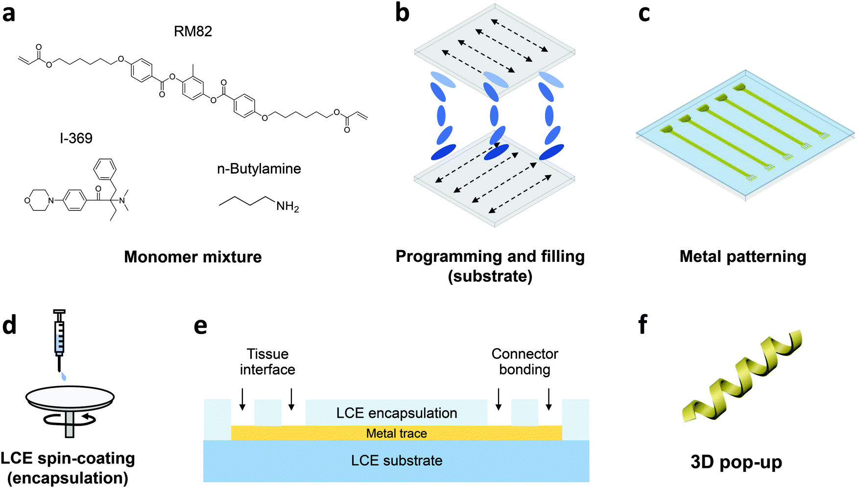 | ||
| Fig. 1 Schematic illustration of fabrication procedure of LCE-based 3D, implantable electronics. (a) Monomer mixture. (b) Programming and filling. (c) Metal patterning. (d) LCE spin-coating. (e) Selective metal exposure. (f) 3D pop-up. | ||
To examine the viability of LCE for use in long-term implantation, we first evaluated the hydrolytic and oxidative stability of the LCE under accelerated in vitro conditions. A 0.1 M NaOH solution was used for accelerated hydrolytic medium,34 and a 20% H2O2 solution with 0.1 M CoCl2 was used as the accelerated oxidative medium.34–36 Samples in both conditions were tested at 37 °C for 24 days. We note that at 37 °C, the LCE is in the nematic state and above its glass transition temperature (Tg = 15 °C, Fig. S1, ESI†). In the hydrolytic condition (0.1 M NaOH), LCE films exhibited a minimal decrease in wet mass by 0.43 ± 0.18% (mean ± SD, n = 4) during this period (Fig. 2a). The final mass after drying on day 24 was decreased by 0.81 ± 0.07% (mean ± SD, n = 4) (Table 1), indicating minor degradation of the LCE films in the hydrolytic condition, despite the fact that these materials are polyesters. We hypothesized that the observed hydrolytic stability of LCE arises from both the liquid crystallinity and the intrinsic hydrophobicity of this material. As no process exists to maintain the chemistry of the network while changing the phase of the materials at 37 °C, we synthesized two control networks and subjected them to the same degradation tests. Briefly, one control network was synthesized by replacing 36 mol% of the RM82 with bisphenol A ethoxylate diacrylate (Fig. S2a, ESI†); this was denoted BPAEDA control. The other control network was synthesized by replacing 36 mol% of the RM82 with tricyclo[5.2.1.02,6]decanedimethanol diacrylate (Fig. S2b, ESI†); this was denoted TCMDA control. Both control networks are amorphous at room temperature and body temperature. The first control is comprised of aromatic acrylics, like the LCE, but is somewhat more polar due to the ethoxylates. The second control network is expected to be less polar than the LCE, but it is also less aromatic. Both of the control materials are poly(β-amino ester) networks formed with the same chain extender and acrylate-to-amine ratio as the LCE. In the hydrolytic condition (0.1 M NaOH), both of the controls showed a slightly more noticeable decrease both in wet mass and dry mass than LCE during the same periods (Fig. 2a and Table 1). However, there was no significant difference in the mass losses between the two controls. These results suggest that the liquid crystallinity of LCE contributes marginally to hydrolytic stability, while noting that for these hydrophobic polyesters hydrolysis is quite slow.
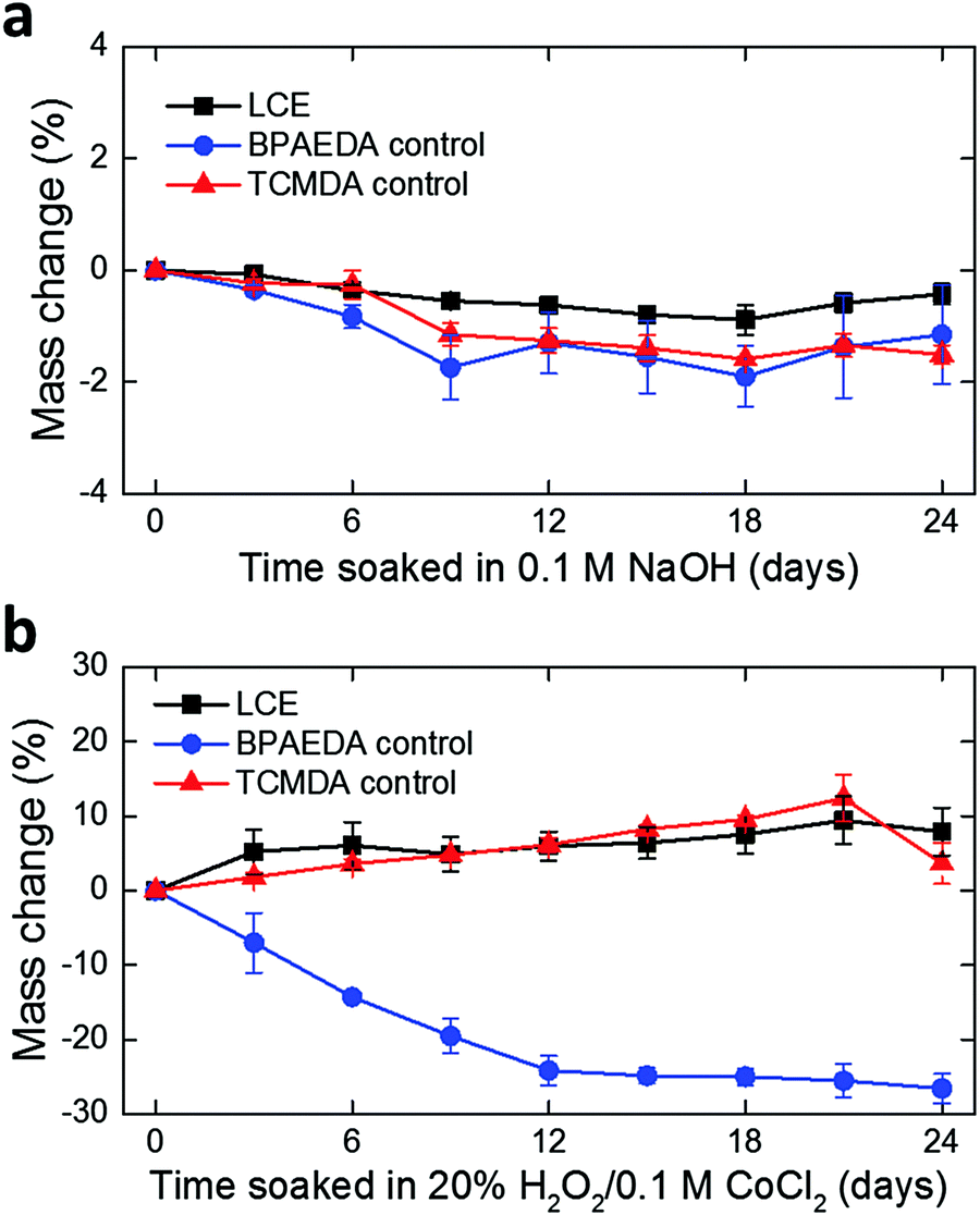 | ||
| Fig. 2 Monitoring of mass change in LCE and control films over 24 days in (a) 0.1 M NaOH (mean ± SD, n = 4) and (b) 20% H2O2/0.1 M CoCl2 (mean ± SD, n = 4), both at 37 °C. | ||
| 0.1 M NaOH | 20% H2O2/0.1 M CoCl2 | |
|---|---|---|
| LCE | 0.81 ± 0.07% | 9.48 ± 5.54% |
| BPAEDA control | 1.66 ± 0.54% | Lost integrity |
| TCMDA control | 1.19 ± 0.07% | Lost integrity |
Polymers containing tertiary amines in the backbone, such as these poly(β-amino ester) networks, are susceptible to oxidation in vivo.34 In the oxidative condition (20% H2O2 in 0.1 M CoCl2), LCE films showed an increase in wet mass by 7.99 ± 3.22% (mean ± SD, n = 4) (Fig. 2b). The increase in mass combines both mass loss and water uptake. After completely drying on day 24, however, the final mass appeared to be 9.48 ± 5.54% (mean ± SD, n = 4) lower than the initial mass (Table 1). These dried samples were further characterized by attenuated total reflection Fourier transform infrared (ATR-FTIR) spectroscopy and compared with as-prepared LCE that did not undergo oxidative degradation (Fig. S4, ESI†). Two distinct changes in the FTIR spectra were observed: (1) shift and broadening of the carbonyl peak (1724 cm−1) to lower wavenumber and (2) appearance of a broad O–H stretching band near 3300 cm−1, indicating the presence of carboxylic acids and alcohols, respectively, in this oxidized LCE. These carboxylic acid and alcohol groups may result from hydrolysis of esters after oxidation enables water ingress into the LCE. In the case of the control networks, the BPAEDA controls exhibited a large decrease in wet mass by 26.57 ± 1.98% (mean ± SD, n = 4) in this oxidative condition while the TCMDA controls showed a similar amount of increase in wet mass as LCE (Fig. 2b). Notably, after completely drying on day 24, both of the control networks were physically broken down and lost integrity (Table 1). This indicates that the liquid crystallinity likely plays a significant role in the relative oxidative stability of LCE as compared to the amorphous controls. This oxidative sensitivity under aggressive accelerated aging conditions represents a potential failure mode for LCE-based implantable electronics. We also separately carried out real-time degradation tests for LCE and the control networks over 48 days. A PBS solution was used for real-time hydrolytic medium34 and a 3% H2O2 solution was used for real-time oxidative medium,34,37 both at 37 °C. Similar trends in mass change were observed in LCE and control networks as the cases in the accelerated conditions (Fig. S3a, b and Table S1, ESI†).
It is important to note that the 24 day period used in the accelerated hydrolytic tests with the 0.1 M NaOH medium simulates roughly >1 year in vivo. More specifically, it has been reported that 1 day in 0.005 M NaOH at 37 °C approximates 3 weeks of implantation (i.e., 24 days approximate 72 weeks).38 It is, therefore, likely that 24 days in 0.1 M NaOH at 37 °C simulates at least 72 weeks (1.4 years) or longer in vivo. Likewise, the 20% H2O2/0.1 M CoCl2 accelerated oxidative system has been reported to provide a strong correlation between the in vitro and in vivo results, where 24 days in the 20% H2O2/0.1 M CoCl2 medium approximated 12 months of implantation for selected polyurethane compositions in rats.36,39 While the presented results do not suggest that the observed mass losses of LCE under the hydrolytic and oxidative conditions are acceptable for implantable electronics, they do suggest that long-term implantation of LCE is possible. Further examination of the degradation of LCE-metal multilayer devices under these chemical conditions is necessary to confirm the viability of LCE-based electronics for use in chronic implantation.
For chronic implantation of electronics, device encapsulation is critical to isolate the underlying metallic components from conductive bodily fluids. Polymer coatings, such as parylene-C and polyimide, have been preferred options for encapsulation of flexible neural implants.40–44 However, the integration of these insulating polymers onto responsive polymers is likely to lead to interfacial pathways for fluid ingress.45,46 Here, we use spin-coated LCE as an encapsulation material, leveraging its good intrinsic barrier properties as well as a potential for providing covalent bonding to the LCE substrate. Based on prior studies, we targeted an encapsulation layer in the range of 1–5 μm. This thin layer should minimally alter the shape change of the underlying substrate and be compatible with microfabrication while providing a high barrier. Briefly, the spin-coating process consists of (1) preparation of liquid crystal oligomer dissolved in toluene, (2) spin-coating, and (3) UV-curing in a nitrogen ambient environment (Fig. 3a). Using this method, spin-coated LCE films in the range of 1.5–6.8 μm were achieved by varying the LC oligomer concentration (with respect to toluene) and the rotation speed (Fig. 3b). The spin-coated LCE adopted a polydomain nature both on a gold trace (Fig. 3c) and on aligned LCE substrates (Fig. 3d), indicating that it should be mechanically passive.
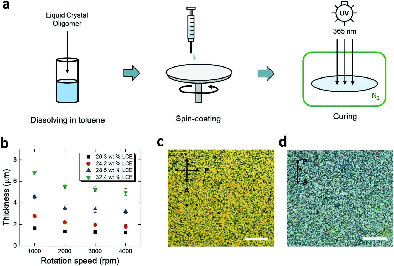 | ||
| Fig. 3 (a) Schematic illustration of LCE spin-coating process. (b) Thickness of spin-coated LCE films as functions of LCE concentration and rotation speed (mean ± SD, n = 3). Polarized optical micrographs of spin-coated LCE (c) on a gold trace (viewed in reflection mode) and (d) on a twisted nematic LCE substrate (viewed in transmission mode). (Scale bars = 30 μm.) | ||
The processing approach (Fig. 1 and 3) described here allows for the fabrication of encapsulated LCE electronics in 2D and various 3D shapes. Multichannel electrode arrays were implemented on ‘flat’ (Fig. 4a), ‘twisted’ (Fig. 4b), and ‘wavy’ LCE substrates (Fig. 4c). While the flat geometry was obtained from non-aligned (i.e., polydomain) LCE films, the twisted and wavy geometries were created by programming the molecular orientation of LCE films with variation through the thickness (twisted) or both through the thickness and within the plane of the substrate (wavy), as described in a recent publication.30 It should be emphasized that the formation of these 3D shapes occurs spontaneously upon release of the LCE substrates from the carrier glass after the entire device fabrication is complete, as this shape change is caused by the anisotropic and heterogeneous thermal dimensional changes of the programmed LCE. The fabricated devices in all three substrate geometries (flat, twisted, wavy) have 16-channel signal traces (inset of Fig. 4a) and exposed gold microelectrodes (inset of Fig. 4b), mimicking the configuration of microelectrode arrays for neural recording. The polarized optical micrographs (POM) showed characteristic dark and bright optical patterns when rotating the twisted and wavy samples between parallel polarizers (Fig. 4b and c, bottom images); this confirms successful fabrication of electronics on twisted nematic 2D LCE substrates. Alignment was not observed for the electronics on the polydomain LCE substrate (Fig. 4a, bottom image), as expected. These POMs confirm the controlled molecular orientation of the LCE enabled by the photoalignment of the underlying light-sensitive dye.
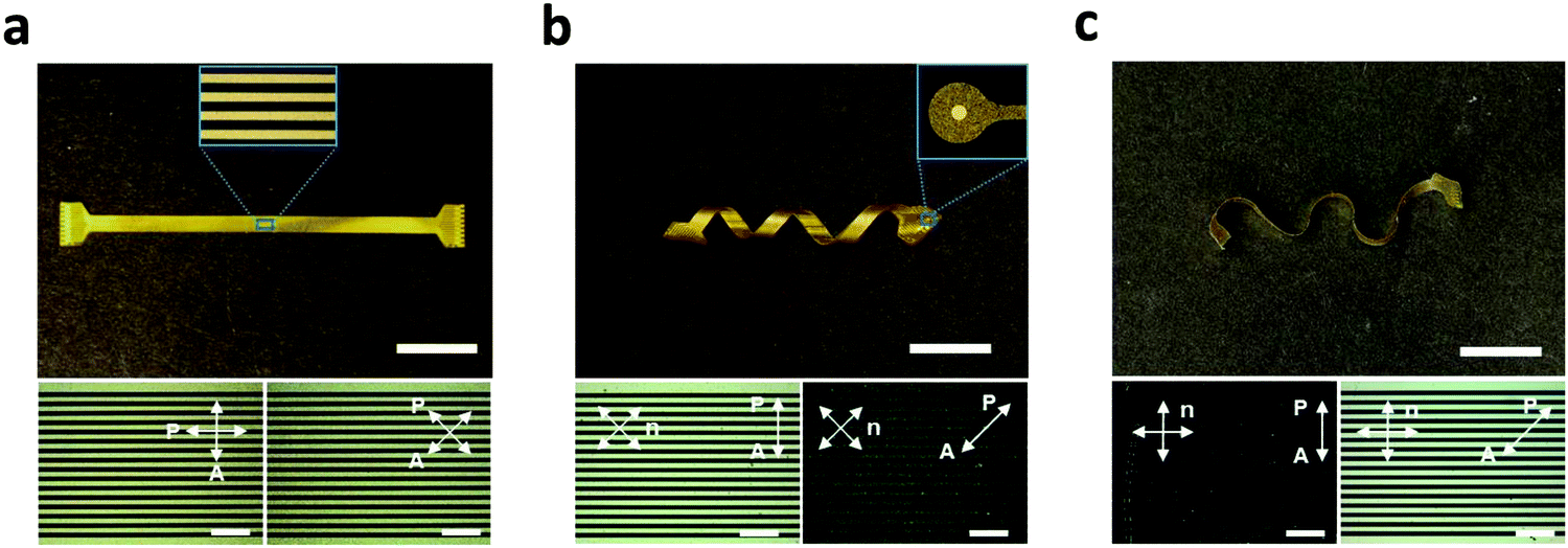 | ||
| Fig. 4 Photo images of 16-channel multielectrode arrays fabricated on LCE substrates in various 2D and 3D shapes. (a) ‘Flat’. Inset shows multichannel gold traces. (Scale bar = 1 cm.) (b) ‘Twisted’. Inset shows exposed site of gold microelectrode. (Scale bar = 1 cm.) (c) ‘Wavy’. (Scale bar = 1 cm.) The bottom images are polarized optical micrographs of each device. (Scale bars = 500 μm.) | ||
We assessed the electrochemical stability of the fabricated LCE electronics. Specifically, we soaked the twisted and flat devices in PBS at 37 °C and carried out daily electrochemical impedance spectroscopy (EIS) measurements for 67 days. These conditions were selected to simulate physiological conditions for a sufficient period for sub-chronic studies.47,48 Over the duration of the study, both the twisted and flat devices maintained relatively stable impedance spectra shape and magnitude (Fig. 5a and b). The impedances of electrodes at 1 kHz are of particular interest49–51 as action potentials have a characteristic frequency band centered at 1 kHz.49 Initial impedance magnitudes of the twisted and flat devices at 1 kHz averaged to 124.3 ± 20.7 kΩ (mean ± SEM, n = 27) and 79.9 ± 25.9 kΩ (mean ± SEM, n = 15), respectively (Fig. 5c). In the case of twisted devices, the final recorded impedance magnitude at 1 kHz averaged to 164.2 ± 30.6 kΩ (mean ± SEM, n = 27), showing no significant difference (t-test, p = 0.28, n = 27) between the initial and final time points (Fig. 5c). In the case of flat devices, the final recorded impedance magnitude at 1 kHz was 147.5 ± 21.4 kΩ (mean ± SEM, n = 15), also showing no significant difference (t-test, p = 0.054, n = 15) from the initial value (Fig. 5c). These results demonstrate that the spin-coated LCE encapsulation layer serves as an effective barrier to ionic aqueous solutions, regardless of the shape of the underlying substrate. However, it is notable that oxidative degradation does induce some shape change in the LCE substrate (Fig. S6, ESI†). This shape distortion is likely due to the swelling of the LCE during oxidation (as discussed in Fig. 2b). Overall, the 1 kHz impedance values measured here (approximately 50–200 kΩ) are suitable for neural recording. We separately assessed the insulating properties of spin-coated LCE in comparison with parylene-C. Similar 16-channel multielectrode arrays were fabricated on flat LCE substrates with a 2 μm-thick parylene-C coating and characterized under the same electrochemical conditions. parylene-C was selected as a control due to its wide use as a coating material for neural interfaces.40–42 Initial impedance magnitude of parylene-C encapsulated devices at 1 kHz averaged to 131.0 ± 26.2 kΩ (mean ± SEM, n = 13), similar to the LCE encapsulated devices (Fig. S5, ESI†). However, the impedance magnitude at 1 kHz significantly decreased (t-test, p = 0.022, n = 13) to 57.0 ± 15.0 kΩ (mean ± SEM, n = 13) by day 2 and did not return to baseline (Fig. S5, ESI†). This early impedance drop could be attributable to the water leakage occurring through the interface between the LCE substrate layer and the parylene-C encapsulation layer. In contrast, this impedance drop was not observed in the LCE encapsulated devices. These results again suggest that the spin-coated LCE provides sufficient insulation for use in implantable electronics.
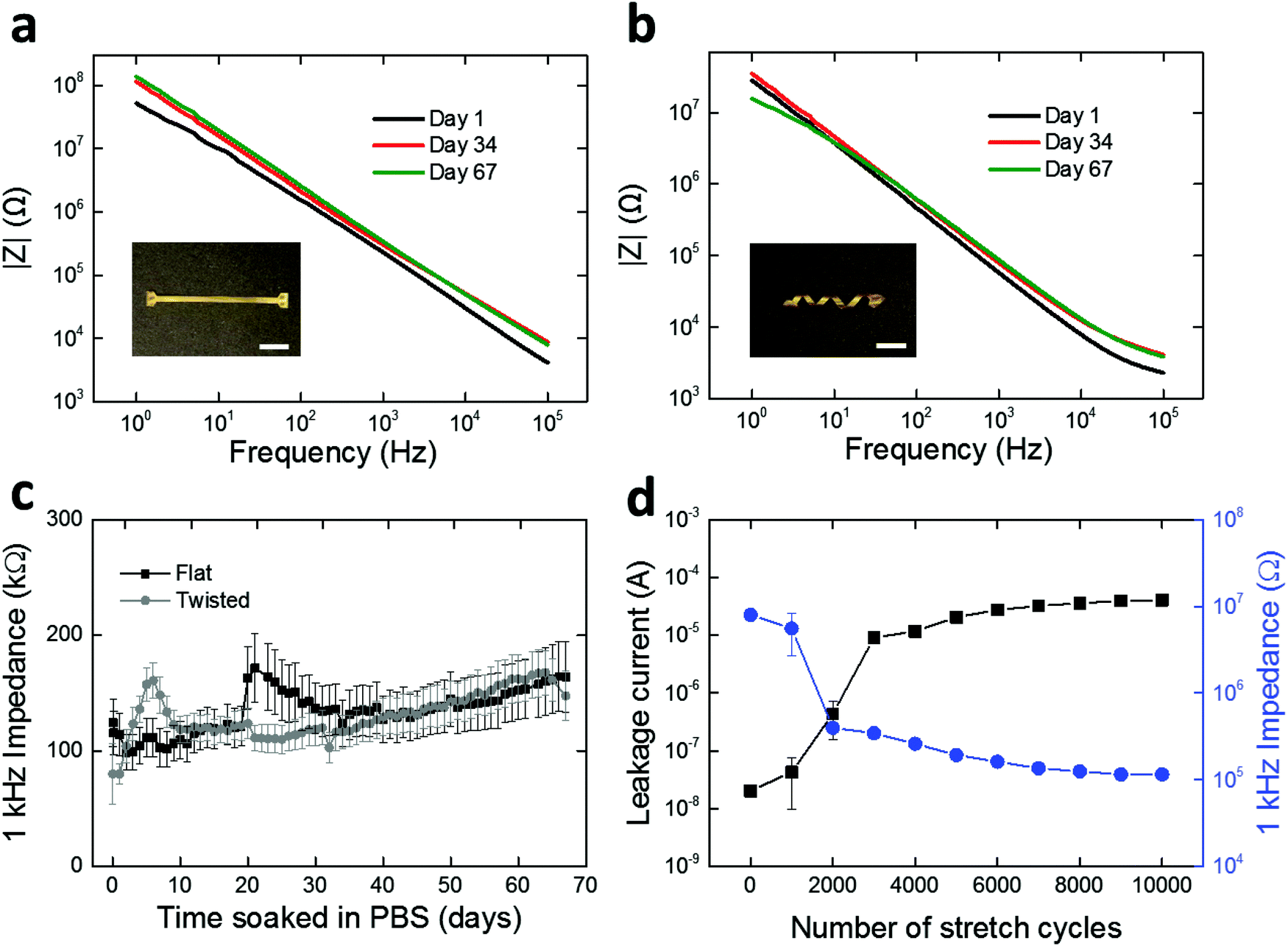 | ||
| Fig. 5 Representative electrochemical impedance spectra of gold microelectrodes on (a) flat and (b) twisted LCE substrates on day 1, 34, and 67. Insets show the devices characterized. (Scale bars = 1 cm.) (c) Daily monitoring of 1 kHz impedance of gold electrodes on flat and twisted devices over 67 days (mean ± SEM, n = 15). (d) Monitoring of leakage current and 1 kHz impedance of closed (encapsulated) gold electrodes on twisted devices under cyclic stretching (60% strain) over 10000 cycles (mean ± SD, n = 32). All measurements were carried out in PBS at 37 °C. | ||
While we have so far demonstrated the electrochemical stability of the LCE electronics under physiological solutions in stationary conditions, the in vivo environment is dynamic, and thus these devices, once implanted, will need to deform with the body. These 3D devices, unlike typical planar electronics, can stretch without inducing large deformations in the relatively fragile gold conductors. To model these circumstances, we further evaluated the stability of LCE electronics under cyclic mechanical stretching (60% strain) up to 10000 cycles while being soaked in PBS at 37 °C. Twisted, 16-channel devices were fabricated without opening the encapsulation layer to expose the gold electrode sites. After fabrication and for the first 1000 cycles to 60% strain, the devices exhibited high 1 kHz impedance (∼107 Ω), typical of a fully encapsulated device. A noticeable decrease in the 1 kHz impedance (8.0 × 10⁶ Ω → 3.4 × 10⁵ Ω) occurred between 1000 and 2000 cycles of stretching (Fig. 5d), which suggests the creation of leakage pathways in the insulation. This was further supported by the leakage current measurements where a considerable increase in DC current (2.0 × 10⁻⁸ A → 9.1 × 10⁻⁶ A) was observed during the first 3000 cycles (Fig. 5d). After 3000 cycles, however, both the impedance and leakage current maintained at a relatively stable level up to 10000 cycles. While this mechanical aging under extreme conditions (10000 cycles of 60% strain) does capture potential failure modes of these devices, we note that the integrity of the conductors remains intact and that these long cables (trace length = 50 mm) maintain sufficient insulating properties to be used with electrodes of lower impedance, such as those used for recording and stimulating nerves in the periphery.
Finally, we demonstrate LCE electronics as deformation-tolerant interconnection cables for applications in neural interfaces. Achieving interconnection cables that can reliably connect the implants to the outside world is critical for chronic neural interfaces.9,43,52 As such, 4-channel LCE cables with flat (Fig. S8a, ESI†), wavy (Fig. S8b, ESI†), and twisted (Fig. 6a) geometries were fabricated and assembled with a commercially-available 4-channel nerve cuff and connector. The nerve cuff possesses 4 neural recording electrodes that are coated with 200 nm-thick titanium nitride (TiN), to form a low-impedance electrode suitable for stimulation or recording. To assess the effect of deformation on the electrochemical stability of the LCE cable under mechanical loading conditions, a custom-built load cycling setup was utilized (Fig. S7, ESI†). Briefly, cables were subjected to cyclic stretching (elongation) or buckling (compression) at 60% strain up to 10000 cycles, while being soaked in PBS at 37 °C. The flat-cabled cuffs immediately failed after 1 cycle of stretching (data not shown), as expected. Under buckling, the flat-cabled cuffs generally maintained a stable 1 kHz impedance level up to 10000 cycles but showed failure in 25% of their electrode channels (Fig. S8a, ESI†). The wavy-cabled cuffs generally maintained a stable 1 kHz impedance level over 10000 stretching cycles but also showed failure in 25% of the channels (Fig. S8b, ESI†). In the case of twisted-cabled cuffs, initial impedance magnitudes at 1 kHz averaged to 0.4 ± 0.01 kΩ (mean ± SEM, n = 5) under stretching, and 0.4 ± 0.02 kΩ (mean ± SEM, n = 3) under buckling (Fig. 6b). We note that these impedance values are typical for TiN electrodes at this size scale (geometric surface area ∼0.4 mm2), which confirms the good electrical connection between the LCE cable, the nerve cuff, and the connector. The final impedance magnitudes at 1 kHz averaged to 0.4 ± 0.01 kΩ (mean ± SEM, n = 5) under stretching, and 0.4 ± 0.01 kΩ (mean ± SEM, n = 3) under buckling (Fig. 6b). There was no significant change when comparing the initial and final values under either stretching (t-test, p = 0.47, n = 5) or buckling (t-test, p = 0.18, n = 3). On further examination, the EIS impedance and phase spectra showed no observable change over 10000 stretching cycles (Fig. 6c). We presume that the LCE cables may have undergone minor leakage during these cycling conditions as discussed above in Fig. 5d; however, the effect does not appear here as the impedance of the TiN electrodes on the cuffs (∼400 Ω) is lower than that of the LCE cables after mechanical aging (>105 Ω) by more than two orders of magnitude. These results suggest that the electrochemical integrity of the twisted-cabled cuffs was not compromised under extended cycles of mechanical loading. This is critical to the success of future implantable electronics, in particular for neural interfaces in the peripheral nervous system.
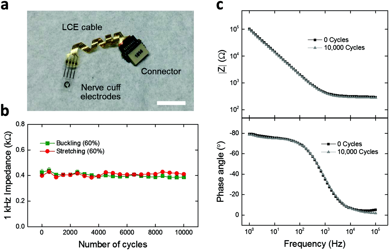 | ||
| Fig. 6 (a) Photo image of 4-channel nerve cuff electrodes assembled to a connector using a twisted LCE cable. (Scale bar = 1 cm.) (b) Monitoring of 1 kHz impedance of the assembled nerve cuff device under cyclic stretching or buckling (60% strain) over 10000 cycles (mean ± SEM, n = 5 for stretching and n = 3 for buckling). (c) Representative electrochemical impedance magnitude and phase spectra of the assembled nerve cuff device at 0 and 10000 stretching cycles. All measurements were carried out in PBS at 37 °C. | ||
Experimental
LCE substrate preparation
LCE substrates with programmed molecular alignment were prepared by a photoalignment method as previously reported.30 Glass slides (75 mm × 51 mm × 1.2 mm, Electron Microscopy Sciences) were cleaned by sonication for 5 min each in Alconox (Alconox Incorporation), acetone, isopropanol, and deionized water and subsequently dried with nitrogen. The cleaned glass slides were treated with oxygen plasma (Sirius T2, Trion Technology) for 1 min at a pressure of 100 mTorr and a power of 50 W. 1 wt% of a photoalignable dye, brilliant yellow (Sigma Aldrich), was dissolved in dimethylformamide (DMF, Fisher Scientific) then filtered by a 0.45 μm pore size sterile syringe filter (Whatman). The brilliant yellow solution was spin-coated onto the glass slides at 750 rpm (1500 rpm s−1) for 10 s and at 1500 rpm (1500 rpm s−1) for 30 s. This coating layer serves as the alignment layer whose orientation ultimately controls the alignment of nematic liquid crystal.For photoalignment, the glass slides were exposed to a linearly-polarized broadband light at an intensity of 10 mW cm−2 for 2 min. Specifically, these slides were placed in a sample holder in series with a rotatable polarizer and a projector (Vivitek D912HD) and patterned by selectively exposing regions of the slide to different polarizations of light. To program ‘twisted’ geometry (Fig. 4b), a pair of glass slides were entirely exposed to a bright light using 45° polarizer. After exposure, the two glass slides were assembled 38 μm apart using film spacers (Precision Brand) to form a cell in such a way that (1) the exposed side of the two glass slides face each other and (2) the incident angles on the two glass slides are 90° each other while one is +45° and the other is −45° with the orientation of long edges of the glass slides. To program ‘wavy’ geometry (Fig. 4c), a pair of glass slides were selectively exposed to an in-plane pattern consisting of alternating bright and dark regions while using 90° polarizer for one slide and 0° polarizer for the other slide. After exposure, the two glass slides were assembled 38 μm apart to form a cell in such a way that (1) the exposed side of the two glass slides face each other and (2) the incident angles on the two glass slides are 90° each other while one is 0° and the other is 90° with the orientation of long edges of the glass slides. To program ‘flat’ geometry (Fig. 4a), a pair of glass slides were directly assembled 38 μm apart to form a cell without exposing to polarized light.
A liquid crystal monomer, 1,4-bis-[4-(6-acryloyloxyhexyloxy)-benzoyloxy]-2-methylbenzene (RM82, Wilshire Chemicals), a chain extender molecule, n-butylamine (nBA, Sigma Aldrich), and a photoinitiator, Irgacure I-369 (BASF) were mixed using a molar ratio of 1.1:1 between RM82 and nBA with 1.5 wt% of the photoinitiator. The mixture was heated and vortexed, then filled into the photopatterned cell by capillary action. The cell was kept in a digital lab oven (Quincy Lab, Inc.) at 65 °C for 15 h for oligomerization. The oligomers were cross-linked by exposing to a 365 nm UV light (OmniCure® LX400+, Lumen Dynamics) on a 90 °C hot plate (twisted and wavy) or at room temperature (flat) at an intensity of 250 mW cm−2 for 5 min. After cross-linking, the topside glass slide was gently removed to leave an LCE film that served as a substrate.
Optical and thermal characterization
A polarizing optical microscope (Olympus, BX51) was used for optical characterization of LCE molecular alignment. Differential scanning calorimetry (Mettler Toledo) was carried out for thermal analysis of the LCE. Samples were loaded into aluminium pans and scanned from −50 to 150 °C with ramps of ±10 °C min−1. Only the second heating cycle was shown.Chemical degradation tests
Solutions of 0.1 M NaOH and 20% H2O2/0.1 M CoCl2 were used for accelerated hydrolysis and oxidation, respectively, both at 37 °C. PBS and 3% H2O2 solutions were used for real-time hydrolysis and oxidation, respectively, also at 37 °C. A 0.1 M NaOH solution was prepared by mixing 400 mg of NaOH with 100 mL of reverse osmosis (RO) water. A 20% H2O2 solution in 0.1 M CoCl2 was prepared by (1) dissolving 325 mg of CoCl2 in 10 mL of RO water, (2) mixing 50 mL of 30% H2O2 with 15 mL of RO water, and (3) mixing the two solutions together. A 3% H2O2 solution was prepared by diluting 10 mL of 30% H2O2 in 90 mL of RO water. LCE films were soaked in these solutions, and the degradation of the films was examined by monitoring the mass change over 24 days (accelerated) or 48 days (real-time). Specimens were taken out of the solutions every 3 days and the wet mass was measured. All solutions were changed every 3 days. On the last day of evaluation, in addition to the wet mass, the final mass was also measured after completely drying the specimens in a vacuum oven at 50 °C for 12 h.BPAEDA control networks were synthesized by replacing 36 mol% of the RM82 with bisphenol A ethoxylate diacrylate while maintaining the same chain extender (nBA) and acrylate-to-amine molar ratio (1.1:1) as LCE. TCMDA control networks were synthesized by replacing 36 mol% of the RM82 with Tricyclo[5.2.1.02,6]decanedimethanol diacrylate while also maintaining the same chain extender (nBA) and acrylate-to-amine molar ratio (1.1:1) as LCE.
LCE spin-coating
Spin-coated LCE was obtained as follows. A mixture of RM82, nBA, and I-369 was prepared and oligomerized in an oven at 65 °C for 15 h, as described above. This LC oligomer was then dissolved in toluene and filtered using a 0.45 μm pore size sterile syringe filter (Whatman) for use in spin-coating. After being dispensed onto a target sample and rotated, the spin-coated film was heated at 85 °C for 5 min for evaporation of toluene. Finally, the spin-coated film was polymerized under exposure to a 365 nm UV light (OmniCure® LX400+, Lumen Dynamics) at an intensity of 250 mW cm−2 for 150 s in a nitrogen gas ambient at room temperature. It is important to note that introducing nitrogen and thus eliminating oxygen during UV exposure is critical to achieving polymerization of spin-coated LCE, as oxygen inhibits free-radical photopolymerization.53For thickness evaluation of spin-coated LCE, the weight ratio of the LC oligomer with respect to toluene was varied. For 20.4 wt% LCE, 889 mg of oligomer (800 mg RM82 mixed with 75.9 mg nBA and 13.1 mg I-369) was dissolved in 3480 mg of toluene. For 24.2 wt% LCE, 1111.3 mg of oligomer (1000 mg RM82 mixed with 94.9 mg nBA and 16.4 mg I-369) was dissolved in 3480 mg of toluene. For 28.5 wt% LCE, 1389.2 mg of oligomer (1250 mg RM82 mixed with 118.7 mg nBA and 20.5 mg I-369) was dissolved in 3480 mg of toluene. For 32.4 wt% LCE, 1667.0 mg of oligomer (1500 mg RM82 mixed with 142.4 mg nBA and 24.6 mg I-369) was dissolved in 3480 mg of toluene. The rotation speed was also varied as 1000, 2000, 3000, and 4000 rpm while maintaining the acceleration speed at 500 rpm s−1. Three samples were prepared for each of these conditions on 25 mm × 25 mm glass slides. To obtain the film thicknesses, LCE films were partially removed from the glass slides manually using a razor blade, then the step heights between the LCE layer and the substrate layer were measured using a Veeco Dektak VIII Profilometer. Five spots were measured for each sample, and the mean values were taken.
LCE 3D cable fabrication
LCE 3D cables were fabricated as follows. First, an aligned LCE film of ∼38 μm thick was prepared on a glass slide by using the method described above. A 200 nm-thick gold layer was deposited onto the LCE film using an AJA ATC 2200 DC magnetron sputtering system and patterned by photolithography and wet etching processes. LCE was spin-coated onto the gold layer and cured to form an encapsulation layer, as described above. To achieve ∼2 μm-thick LCE coating, a 24.2 wt% LC oligomer solution was prepared and spin-coated at 3000 rpm (500 rpm s−1). The gold bond pads were exposed by selectively etching out the spin-coated LCE layer using photolithography and oxygen plasma reactive ion etching (RIE). For device singulation, a SiN layer of ∼800 nm was deposited as a hard mask by using a plasma-enhanced chemical vapor deposition (PECVD) system. The SiN layer was patterned by photolithography and RIE in an SF6 plasma, and the LCE layer was subsequently etched out by RIE in an oxygen plasma. The SiN hard mask was then removed in a 10:1 hydrofluoric acid (HF) solution. Finally, the LCE cables were released from the glass slide by soaking the sample in a 15 wt% potassium borate solution for 30 min, followed by deionized (DI) water washing and air drying. Upon release, the LCE cables spontaneously changed shape from 2D (flat) to 3D according to the molecular alignments programmed as described above. The cables were designed to be 50 mm in length and 2 mm in width at the flat state.
Electrochemical characterization
All LCE cables were characterized by EIS using a CHI 608E potentiostat (CH Instruments, Austin, TX, United States). A sinusoidal potential of 10 mV was delivered between 1 Hz to 100 kHz at 12 points per decade. Leakage current measurements were obtained as previously described.54 Briefly, chronoamperometry (CA) was used to deliver a 5 V DC step pulse signal for 150 s, and the DC leakage current was measured as a response. The devices under test were submerged in PBS in a cell with a two-electrode configuration (ground and working). To age samples, cells were kept in a PBS bath at 37 °C and recorded daily.Mechanical cycling
Mechanical cycling tests were carried out using a custom-built apparatus that is capable of performing stretching or buckling while providing electrochemical measurements within PBS at a specific temperature (Fig. S7, ESI†). The apparatus consists of 4 main components; this includes a Fisherbrand Isotemp advanced stirring hotplate (Thermo Fisher Scientific, Waltham, MA, United States), a stainless steel heating bath, an L12-P Micro linear actuator (Actuonix, Victoria, Canada), and a 3D printed water-tight enclosure. The actuator is connected to a stainless steel arm, which holds the water-tight enclosure, and is capable of compressing and extending the cable repeatedly. An Arduino microcontroller controls the actuator's parameters, such as its speed, displacement, and cycles. LCE cables assembled to nerve cuff electrodes (Fig. 6a) were prepared by connecting one end of the LCE cable to 4-channel Qualia nerve cuff electrodes (Qualia Inc., Richardson, TX, United States) and the other end to the Qualia connector (Qualia Inc., Richardson, TX, United States), both using a commercial conductive epoxy, along with a medical-grade epoxy for encapsulation. The connector was housed within an enclosure to prevent shorting during electrochemical measurements. All test devices were subjected to cyclic stretching or buckling at 60% strain, at a constant speed of 2 seconds per cycle, up to 10000 cycles, while being soaked in PBS at 37 °C.
Conclusions
Biosensors, neural interfaces, and other types of implantable electronics must be able to withstand both the mechanical and chemical conditions in vivo. In this work, we demonstrate that LCEs constitute a class of promising materials that are suitable to serve as substrate and encapsulation layer for devices that withstand the in vivo environment. LCEs are shape programmable materials that can be planar during photolithography and then adopt a predetermined 3D shape. This 3D shape enables devices that are intrinsically inextensible to become extrinsically stretchable. Furthermore, the hydrophobic and ordered nature of the LCE enables these responsive materials to undergo minimal hydrolysis and relatively less oxidative degradation than amorphous polymer networks of similar chemistry. Potential failure mechanisms of the moderate oxidative degradation and mechanically-induced formation of leakage pathways were identified. However, by using twisted nematic LCEs as shape-morphing substrates, we have demonstrated 3D multichannel electrode arrays that tolerate stretching and buckling strains of 60% over 10000 cycles in a physiological medium. This combination of properties is difficult to achieve with traditional materials.
Conflicts of interest
There are no conflicts to declare.Acknowledgements
This research was partially supported by the National Science Foundation under grant no. 1752846 and 1711383 and partially supported by the Defense Advanced Research Projects Agency (DARPA) under contract no. 140D6318C0097. The authors thank Qualia Inc. (Richardson, TX, United States) for providing nerve cuff electrodes and connectors. We also thank Dr Xili Lu for his generous assistance in drawing schematics.Notes and references
- N. G. Hatsopoulos and J. P. Donoghue, Annu. Rev. Neurosci., 2009, 32, 249–266 CrossRef CAS PubMed.
- A. P. F. Turner, Chem. Soc. Rev., 2013, 42, 3184–3196 RSC.
- M. P. Ward, P. Rajdev, C. Ellison and P. P. Irazoqui, Brain Res., 2009, 1282, 183–200 CrossRef CAS PubMed.
- T. D. Y. Kozai, A. S. Jaquins-Gerstl, A. L. Vazquez, A. C. Michael and X. T. Cui, ACS Chem. Neurosci., 2015, 6, 48–67 CrossRef CAS PubMed.
- K. C. Cheung, P. Renaud, H. Tanila and K. Djupsund, Biosens. Bioelectron., 2007, 22, 1783–1790 CrossRef CAS PubMed.
- H. Y. Lai, L. De Liao, C. T. Lin, J. H. Hsu, X. He, Y. Y. Chen, J. Y. Chang, H. F. Chen, S. Tsang and Y. Y. I. Shih, J. Neural Eng., 2012, 9, 036001 CrossRef PubMed.
- S. Lee, W. Y. X. Peh, J. Wang, F. Yang, J. S. Ho, N. V. Thakor, S. C. Yen and C. Lee, Adv. Sci., 2017, 4, 1700149 CrossRef PubMed.
- D. C. Rodger, A. J. Fong, W. Li, H. Ameri, A. K. Ahuja, C. Gutierrez, I. Lavrov, H. Zhong, P. R. Menon, E. Meng, J. W. Burdick, R. R. Roy, V. R. Edgerton, J. D. Weiland, M. S. Humayun and Y. C. Tai, Sens. Actuators, B, 2008, 132, 449–460 CrossRef CAS.
- B. J. Kim, J. T. W. Kuo, S. A. Hara, C. D. Lee, L. Yu, C. A. Gutierrez, T. Q. Hoang, V. Pikov and E. Meng, J. Neural Eng., 2013, 10, 045002 CrossRef CAS PubMed.
- V. Castagnola, E. Descamps, A. Lecestre, L. Dahan, J. Remaud, L. G. Nowak and C. Bergaud, Biosens. Bioelectron., 2015, 67, 450–457 CrossRef CAS PubMed.
- J. R. Capadona, K. Shanmuganathan, D. J. Tyler, S. J. Rowan and C. Weder, Science, 2008, 319, 1370–1374 CrossRef CAS PubMed.
- J. R. Capadona, D. J. Tyler, C. A. Zorman, S. J. Rowan and C. Weder, MRS Bull., 2012, 37, 581–589 CrossRef CAS.
- T. Ware, D. Simon, D. E. Arreaga-Salas, J. Reeder, R. Rennaker, E. W. Keefer and W. Voit, Adv. Funct. Mater., 2012, 22, 3470–3479 CrossRef CAS.
- M. Ecker, A. Joshi-Imre, R. Modi, C. L. Frewin, A. Garcia-Sandoval, J. Maeng, G. Gutierrez-Heredia, J. J. Pancrazio and W. E. Voit, Multifunct. Mater., 2019, 2, 012001 CrossRef.
- D. H. Kim, Z. Liu, Y. S. Kim, J. Wu, J. Song, H. S. Kim, Y. Huang, K. C. Hwang, Y. Zhang and J. A. Rogers, Small, 2009, 5, 2841–2847 CrossRef CAS PubMed.
- R. H. Kim, D. H. Kim, J. Xiao, B. H. Kim, S. Il Park, B. Panilaitis, R. Ghaffari, J. Yao, M. Li, Z. Liu, V. Malyarchuk, D. G. Kim, A. P. Le, R. G. Nuzzo, D. L. Kaplan, F. G. Omenetto, Y. Huang, Z. Kang and J. A. Rogers, Nat. Mater., 2010, 9, 929–937 CrossRef CAS PubMed.
- I. M. Graz, D. P. J. Cotton, A. Robinson and S. P. Lacour, Appl. Phys. Lett., 2011, 98, 124101 CrossRef.
- A. Romeo, Q. Liu, Z. Suo and S. P. Lacour, Appl. Phys. Lett., 2013, 102, 131904 CrossRef.
- S. Lyu and D. Untereker, Int. J. Mol. Sci., 2009, 10, 4033–4065 CrossRef CAS PubMed.
- V. J. Thannickal and B. L. Fanburg, Am. J. Physiol.: Lung Cell. Mol. Physiol., 2000, 279, L1005–L1028 CrossRef CAS PubMed.
- P. D. Ray, B. W. Huang and Y. Tsuji, Cell. Signalling, 2012, 24, 981–990 CrossRef CAS PubMed.
- H. Wermter and H. Finkelmann, E-Polymers, 2001, 1, 1–13 Search PubMed.
- Y. Hong, A. Buguin, J. M. Taulemesse, K. Kaneko, S. Méry, A. Bergeret and P. Keller, J. Am. Chem. Soc., 2009, 131, 15000–15004 CrossRef PubMed.
- H. Zeng, O. M. Wani, P. Wasylczyk, R. Kaczmarek and A. Priimagi, Adv. Mater., 2017, 29, 1–7 Search PubMed.
- C. Yuan, D. J. Roach, C. K. Dunn, Q. Mu, X. Kuang, C. M. Yakacki, T. J. Wang, K. Yu and H. J. Qi, Soft Matter, 2017, 13, 5558–5568 RSC.
- Y. Yu and T. Ikeda, Angew. Chem., Int. Ed., 2006, 45, 5416–5418 CrossRef CAS PubMed.
- T. H. Ware, M. E. McConney, J. J. Wie, V. P. Tondiglia and T. J. White, Science, 2015, 347, 982–984 CrossRef CAS PubMed.
- T. J. White and D. J. Broer, Nat. Mater., 2015, 14, 1087–1098 CrossRef CAS PubMed.
- L. T. de Haan, P. Leclère, P. Damman, A. P. H. J. Schenning and M. G. Debije, Adv. Funct. Mater., 2015, 25, 1360–1365 CrossRef CAS.
- H. Kim, J. Gibson, J. Maeng, M. O. Saed, K. Pimentel, R. T. Rihani, J. J. Pancrazio, S. V. Georgakopoulos and T. H. Ware, ACS Appl. Mater. Interfaces, 2019, 11, 19506–19513 CrossRef CAS PubMed.
- K. Wang, C. Liu, S. Member and D. M. Durand, IEEE Trans. Biomed. Eng., 2009, 56, 6–14 Search PubMed.
- S. W. Lee, K. S. Min, J. Jeong, J. Kim and S. J. Kim, IEEE Trans. Biomed. Eng., 2011, 58, 2255–2263 Search PubMed.
- S. E. Lee, S. B. Jun, H. J. Lee, J. Kim, S. W. Lee, C. Im, H. C. Shin, J. W. Chang and S. J. Kim, IEEE Trans. Biomed. Eng., 2012, 59, 2085–2094 Search PubMed.
- A. C. Weems, K. T. Wacker, J. K. Carrow, A. J. Boyle and D. J. Maitland, Acta Biomater., 2017, 59, 33–44 CrossRef CAS PubMed.
- M. A. Schubert, M. J. Wiggins, J. M. Anderson and A. Hiltner, J. Biomed. Mater. Res., 1997, 34, 493–505 CrossRef CAS PubMed.
- E. M. Christenson, J. M. Anderson and A. Hiltner, J. Biomed. Mater. Res., Part A, 2004, 70, 245–255 CrossRef PubMed.
- D. K. Dempsey, C. Carranza, C. P. Chawla, P. Gray, J. H. Eoh, S. Cereceres and E. M. Cosgriff-Hernandez, J. Biomed. Mater. Res., Part A, 2014, 102, 3649–3665 CrossRef PubMed.
- M. B. Browning, S. N. Cereceres, P. T. Luong and E. M. Cosgriff-Hernandez, J. Biomed. Mater. Res., Part A, 2014, 102, 4244–4251 CAS.
- E. M. Christenson, J. M. Anderson and A. Hiltner, J. Biomed. Mater. Res., Part A, 2006, 76, 480–490 CrossRef PubMed.
- J. M. Hsu, L. Rieth, R. A. Normann, P. Tathireddy and F. Solzbacher, IEEE Trans. Biomed. Eng., 2009, 56, 23–29 Search PubMed.
- C. Hassler, R. P. Von Metzen, P. Ruther and T. Stieglitz, J. Biomed. Mater. Res., Part B, 2010, 93, 266–274 Search PubMed.
- B. D. Winslow, M. B. Christensen, W. K. Yang, F. Solzbacher and P. A. Tresco, Biomaterials, 2010, 31, 9163–9172 CrossRef CAS PubMed.
- T. Stieglitz, H. Beutel, M. Schuettler and J. U. Meyer, Biomed. Microdevices, 2000, 2, 283–294 CrossRef.
- Z. Xiang, S. C. Yen, N. Xue, T. Sun, W. M. Tsang, S. Zhang, L. De Liao, N. V. Thakor and C. Lee, J. Micromech. Microeng., 2014, 24, 065015 CrossRef.
- W. Li, D. C. Rodger, P. R. Menon and Y. C. Tai, ECS Trans., 2008, 11, 1–6 CAS.
- S. Murray, C. Hillman and M. Pecht, J. Electron. Packag. Trans. ASME, 2004, 126, 390–397 CrossRef CAS.
- A. Canales, X. Jia, U. P. Froriep, R. A. Koppes, C. M. Tringides, J. Selvidge, C. Lu, C. Hou, L. Wei, Y. Fink and P. Anikeeva, Nat. Biotechnol., 2015, 33, 277–284 CrossRef CAS PubMed.
- T. M. Fu, G. Hong, T. Zhou, T. G. Schuhmann, R. D. Viveros and C. M. Lieber, Nat. Methods, 2016, 13, 875–882 CrossRef CAS PubMed.
- K. A. Ludwig, N. B. Langhals, M. D. Joseph, S. M. Richardson-Burns, J. L. Hendricks and D. R. Kipke, J. Neural Eng., 2011, 8, 014001 CrossRef PubMed.
- A. Golabchi, B. Wu, X. Li, D. L. Carlisle, T. D. Y. Kozai, R. M. Friedlander and X. T. Cui, Biomaterials, 2018, 180, 225–239 CrossRef CAS PubMed.
- A. Joshi-Imre, B. J. Black, J. Abbott, A. Kanneganti, R. Rihani, B. Chakraborty, V. R. Danda, J. Maeng, R. Sharma, L. Rieth, S. Negi, J. J. Pancrazio and S. F. Cogan, J. Neural Eng., 2019, 16, 046006 CrossRef PubMed.
- K. Oh, D. Byun and S. Kim, Biomed. Microdevices, 2017, 19, 76 CrossRef PubMed.
- C. Decker and A. D. Jenkins, Macromolecules, 1985, 18, 1241–1244 CrossRef CAS.
- S. Minnikanti, G. Diao, J. J. Pancrazio, X. Xie, L. Rieth, F. Solzbacher and N. Peixoto, Acta Biomater., 2014, 10, 960–967 CrossRef CAS PubMed.
Footnotes |
| † Electronic supplementary information (ESI) available. See DOI: 10.1039/d0tb00471e |
| ‡ J. M. and R. T. R. contributed equally to this work. |
| § Current address: Sensors and Electron Devices Directorate, CCDC Army Research Laboratory, 2800 Powder Mill Road, Adelphi, MD 20783, USA. |
| This journal is © The Royal Society of Chemistry 2020 |