
Novel two-dimensional crystalline carbon nitrides beyond g-C3N4: structure and applications
Li
Tan†
a,
Chunyang
Nie†
a,
Zhimin
Ao
 *a,
Hongqi
Sun
b,
Taicheng
An
a and
Shaobin
Wang
*c
*a,
Hongqi
Sun
b,
Taicheng
An
a and
Shaobin
Wang
*c
aGuangdong Key Laboratory of Environmental Catalysis and Health Risk Control, Guangzhou Key Laboratory of Environmental Catalysis and Pollution Control, School of Environmental Science and Engineering, Institute of Environmental Health and Pollution Control, Guangdong University of Technology, Guangdong 510006, China. E-mail: zhimin.ao@gdut.edu.cn
bSchool of Engineering, Edith Cowan University, Joondalup, WA 6027, Australia
cSchool of Chemical Engineering and Advanced Materials, The University of Adelaide, Adelaide, SA 5005, Australia. E-mail: Shaobin.wang@adelaide.edu.au
First published on 17th September 2020
Abstract
Two-dimensional (2D) crystalline carbon nitrides (CxNy) with graphene-like atomic structures but semiconducting nature are new appealing materials, and increasing interest has been focused on their synthesis, properties, and applications. Apart from the well-known graphitic carbon nitride (g-C3N4), other types of 2D CxNy nanocrystals including C2N, C3N and C5N2 are also successfully fabricated in recent years and their properties and potential uses in various fields have been widely investigated. Meanwhile, g-CN, C2N2, C2N3 and C5N have been theoretically predicted, and their properties and potential applications have also been researched. Until now, 2D crystalline CxNy compounds have demonstrated promising applications in photocatalysis, electrocatalysis, gas adsorption/separation, and energy storage devices, from both experimental and theoretical aspects, stemming from their unique geometric structures, tunable electronic properties, and high specific surface area. Herein, recent advances in the synthesis of 2D CxNy nanocrystals and their applications in various fields are summarized. Moreover, future challenges and opportunities for developing 2D CxNy nanocrystals for more broad applications including environmental remediation are also discussed.
 Li Tan | Miss Li Tan obtained her Master's degree in 2018 from Yanshan University (China) and she is now pursuing a PhD degree under the supervision of Prof. Zhimin Ao at the School of Environmental Science and Engineering, Institute of Environmental Health and Pollution Control, Guangdong University of Technology. Her current research interests focus on the synthesis of novel 2D carbon-nitride-based catalysts for the adsorption of volatile organic compounds and their catalytic remediation. |
 Chunyang Nie | Dr Chunyang Nie obtained her Master's degree in 2013 from East China Normal University (China) and PhD degree in 2016 from Universite Paul Sabatier (France) under the supervision of Dr Emmanuel Flahaut and Dr Marc Monthioux. She joined Prof. Ao's group at the Guangdong University of Technology in 2016 as a Postdoctoral Fellow. Her current research interests focus on the synthesis of novel carbon-based catalysts for aqueous organic pollutant remediation and catalytic mechanisms. |
 Zhimin Ao | Prof. Zhimin Ao received his PhD in Materials Science from Jilin University, China in 2008. He is currently a full professor at the Institute of Environmental Health and Pollution Control, School of Environmental Science and Engineering, Guangdong University of Technology. His research interests mainly focus on the development of environmental catalysts and corresponding mechanism investigation. He has published over 130 SCI papers with citations over 4800 times and an H index of 31. He serves as an Associate Editor of Frontiers in Nanotechnology. |
 Hongqi Sun | Prof. Hongqi Sun received his PhD degree in Chemical Engineering in 2008 from Nanjing University of Technology, China. He joined Edith Cowan University (ECU) in March 2016 and became a full Professor of Chemical Engineering at ECU in November 2017. His research focuses on novel catalysis (photocatalysis, photo-thermal catalysis, photo-electro-chemical catalysis, and membrane catalysis) and advanced oxidation processes (AOPs) over nanostructured materials for solar-to-chemical conversion and environmental remediation. He serves as the Associate Editor of RSC Advances, and Speciality Chief Editor of Frontiers of Nanotechnology, assessor of ARC, committee member of international conferences, and referee of international journals. |
 Taicheng An | Prof. Taicheng An received his PhD in Environmental Science from Sun Yat-sen University, China in 2002. He is currently a full professor and the director of the Institute of Environmental Health and Pollution Control, Guangdong University of Technology. His research interests mainly focus on: (1) synthesis, characterization, optimization and application of nanostructured catalysts and natural mineral materials in environmental remediation; (2) applications of advanced oxidation processes (AOPs); (3) the transportation mechanisms, fate prediction and health effect of emerging organic contaminants. He has been awarded over 70 patents and published over 380 refereed research papers. He serves as an Associate Editor of Appl. Catal. B:Environ. and Ctr. Rev. Env. Tech. |
 Shaobin Wang | Prof. Shaobin Wang obtained his PhD in Chemical Engineering from the University of Queensland, Australia. He is now a Professor at the School of Chemical Engineering and Advanced Materials, The University of Adelaide, Australia. His research interests focus on nanomaterial synthesis and application for adsorption and catalysis, fuel and energy conversion and environmental remediation. He has published more than 400 refereed journal papers with citations over 40 |
1. Introduction
Graphene, as a two-dimensional (2D) atomic crystal available to the scientific community, was successfully discovered by Novoselov in 2004.1 An ideal graphene structure is composed of a single layer of sp2-hybridized carbon atoms.2 Ever since, the applications of this new material have been developed rapidly in many fields such as electronics, photonics, energy storage and conversion, and environmental remediation, arising from its superior electrical and thermal conductivity, chemical stability, mechanical stiffness, and other physical and chemical properties.3 For instance, graphene has been widely studied as an appealing adsorbent for hazardous gases like volatile organic compounds (VOCs), CO2 and aqueous organic pollutants due to its high theoretical specific surface area (SSA, 2630 m2 g−1).4 Additionally, the unique 2D planar structure, large SSA, good electrical conductivity and chemical stability also make graphene an excellent catalyst and support in various catalytic reactions for environmental remediation.4 Moreover, the discovery of graphene has triggered research interest in many other 2D materials.Regardless of the above merits, the zero-bandgap feature of graphene impeded its further applications in electronic devices like switches and light-emitting diodes, and photocatalysis.5 In order to open the bandgap of graphene, diverse structural modifications involving cutting graphene into narrow nanoribbons and doping with heteroelements have been attempted.6 Among them, doping with N atoms is a good option due to the similar relative atomic mass and electron configuration of the N element to the C element, enabling the feasible fitting of N atoms into the covalent carbon matrix.7 However, this chemical modification can inevitably lead to certain damage to the 2D carbon lattice of pristine graphene and the stoichiometry between C and N cannot be easily controlled via the top-down approach.8 With the motivation to supplement the electronic properties of the graphene system with other 2D materials that show similar atomic crystalline structures and intrinsic semiconductivity, bottom-up approaches with C-rich and N-rich precursors to fabricate 2D atomic carbon nitride (CxNy) crystals have been given much attention.9
Research on CxNy was mainly stimulated by the theoretical work of Lu and Cohen in 1989, which postulated that a carbon(IV) nitride (sp3-hybridized) crystal should show comparable or higher hardness than diamond.10 Since then, an exponentially growing number of publications exploring novel CxNy materials from both experimental and theoretical aspects have been reported, while most of them focused on the 3D CxNy-phases and few of them on the 2D crystalline CxNy materials. It was not until 2009 that polymeric graphitic-C3N4 (g-C3N4) was demonstrated as an excellent visible-light-responsive photocatalyst,11 since then more and more efforts have been devoted to the synthesis of 2D g-C3N4 nanosheets via exfoliation of bulk g-C3N4 in order to further enhance the photocatalytic performance.12 Recently, the experimental successes in 2D C2N and C3N crystals pushed the research of 2D CxNy materials to a new high level.13 A large number of attempts have been made on the preparation and potential applications of these new 2D materials as well as prediction of other types of 2D CxNy atomic crystals such as C2N2 and C5N2.14
Currently, 2D CxNy materials show great potential in field-effect transistors (FETs) owing to their semiconducting character, which complements the uses of graphene and insulating 2D boron nitride crystals.13 Meanwhile, the inherent bandgap of 2D CxNy materials makes them potential environment-friendly photocatalysts for different reactions like water splitting, degradation of organic pollutants, CO2 reduction reaction (CO2RR) and so on. Additionally, the introduction of N atoms into the carbon matrix can also break the inertness of pristine graphene and create Lewis basic sites, providing 2D CxNy with good catalytic activity in different reactions. Analogous to graphene, 2D CxNy materials show high theoretical SSAs, good chemical stability and other similar physicochemical properties as well.15 Therefore, they are considered as outstanding adsorbents for gas adsorption and catalyst supports for loading uniformly dispersed nanoparticles.9c,16 In particular, the N atoms in the CxNy network can serve as anchoring sites for isolated metal atoms or dimers, leading to the formation of single atom catalysts (SACs) or double-atom catalysts as a hot topic in recent years.17
To date, a diversity of 2D CxNy materials with different stoichiometric ratios between C and N have been documented in the literature, which include g-C3N4, CN, C2N, C3N, C2N2, C2N3, C5N and C5N2. For these CxNy compounds, the arrangements of C and N atoms in a basic benzene ring and the corresponding structural motif in the sp2-hydridized basal plane differ from each other (the structures of these CxNy materials are shown in Fig. 1). As a result, they exhibit distinct physicochemical properties with respect to the bandgap and texture. Among them, g-C3N4, C2N and C3N have aroused much interest in the field of photocatalysis because they have been already synthesized in laboratories and possess a suitable bandgap and good visible-light adsorption, while the rest of the 2D CxNy compounds are still in the theoretical research stage.
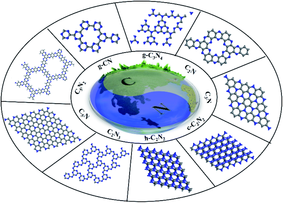 | ||
| Fig. 1 The structures of different 2D CxNy compounds, including g-CN, g-C3N4, C2N, C3N, c-C2N2, h-C2N2, C2N3, C5N and C5N2. | ||
In this work, we present a comprehensive overview of the recent progress in 2D CxNy research. Considering a large quantity of reviews on 2D g-C3N4 in the literature,12a herein, we will focus on the other members of 2D CxNy except g-C3N4, including g-CN, C2N, C3N, C2N2, C2N3, C5N and C5N2. In Sections 2–4, we describe the structural characteristics, experimental synthesis, intrinsic properties and applications (practical and simulated) of C2N, C3N and g-CN, respectively. In Section 5, we will discuss the crystalline structure, electronic properties, and possible applications of C2N2, C2N3, C5N and C5N2. Finally, we go beyond the fundamental properties of these 2D CxNy materials and give an outlook of the promising applications of such materials in more areas including environmental remediation in future.
2. C2N
As early as 1998, Komatsu and Samejima reported the fabrication of amorphous CxNy with a random-layer structure and a chemical composition of C2N through the shock-wave compression of a C- and N-containing polymer.18 In the later decade, little effort was devoted to the synthesis of the 2D C2N crystal. In 2015, Baek et al. demonstrated the successful preparation of a 2D C2N crystal and its crystalline structure with the assistance of advanced characterization tools. Afterwards, a large quantity of experimental and computational studies on 2D C2N have been published due to its peculiar structure and physicochemical properties. In this section, the crystalline structure, synthetic methods, electronic properties, and applications of 2D C2N are summarized.2.1 Crystalline structure of C2N
A C2N monolayer can be considered as a nitrogenated holey graphene layer, in which the benzene rings are connected by nitrogen atoms to constitute large six-membered aromatic rings with two nitrogen atoms facing each other, leading to the formation of periodically uniform holes (Fig. 2).19 All the N atoms in the 2D C2N structure belong to ‘pyridine-type’ or ‘pyrazine-type’ N.9a The primitive cell of the C2N monolayer is shown in Fig. 2, in which three bonds with different lengths are labeled.20 The optimized lattice parameter (the inter-hole distance) is determined to be 8.30 Å by density functional theory (DFT) calculations. However, the lengths of C–N, C–C (1) and C–C (2) bonds vary slightly in different theoretical studies. For instance, Du et al.21 reported that the lengths of C–N, C–C (1) and C–C (2) bonds were calculated to be 1.336 Å, 1.429 Å and 1.470 Å, respectively, whereas Gong et al.20 proposed that the lengths of the three bonds were estimated to be 1.339 Å, 1.432 Å, and 1.469 Å, respectively.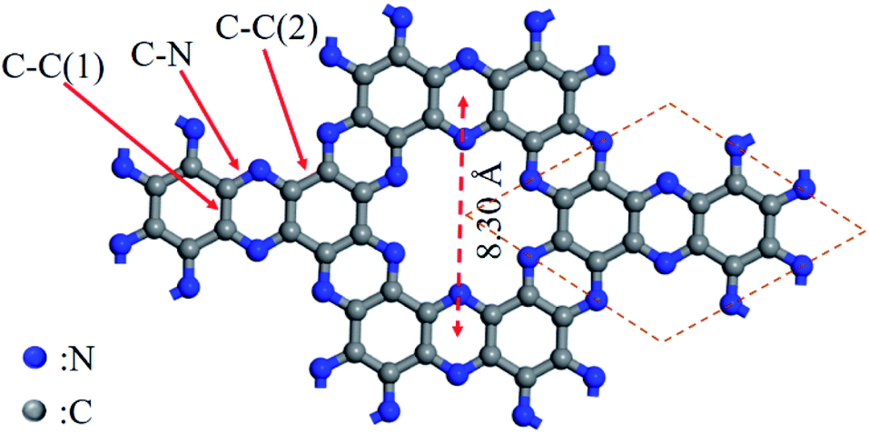 | ||
| Fig. 2 The monolayer structure of the C2N cell. | ||
2.2 Synthesis of C2N
The first synthesis report of the 2D C2N crystal was given by Baek and co-workers in 20159a using the wet-chemical reaction of hexaaminobenzene (HAB) trihydrochloride and hexaketocyclohexane (HKH) octahydrate in N-methyl-2-pyrrolidone (NMP) with sulphuric acid or trifluoromethanesulphonic acid. Due to the spontaneous polycondensation between HAB and HKH, a layered crystalline 2D network structure was formed (Fig. 3a), referred to as the ‘C2N holey 2D crystal’ or ‘C2N-h2D crystal’. The 2D C2N crystalline structure was validated by a series of characterization tools including X-ray diffraction (XRD), X-ray photoelectron spectroscopy (XPS), elemental analysis and electron microscopy (Fig. 3b–h).9a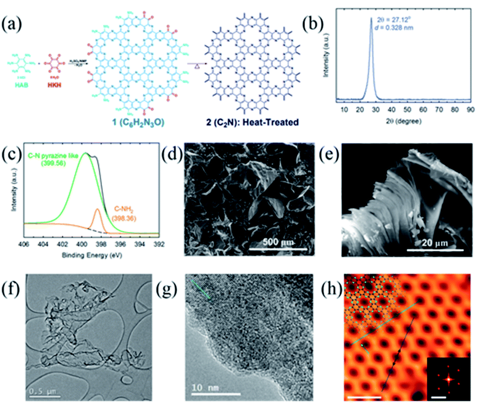 | ||
| Fig. 3 The schematic representation of the C2N-h2D crystal and its characterization: (a) the schematic representation of the C2N-h2D crystal; (b) XRD pattern, (c) XPS survey spectrum, (d) SEM image, and (e) SEM image of heat-treated C2N-h2D flakes; (f) TEM image, (g) high-resolution TEM image, and (h) STM topography image of the C2N-h2D crystal, top-left inset is the structure of the C2N-h2D crystal superimposed on the image. The scale bars and the inset are 2.0 nm, 2.0 nm−1. Reprinted with permission from ref. 9a copyright 2015, Springer Nature. | ||
The XRD pattern (Fig. 3b) revealed that the C2N-h2D crystal was well-crystallized with an interlayer distance of 0.328 nm. Notably, this interspace is slightly lower than that of graphite (0.335 nm),22 attributed to the stronger interlayer interactions. XPS analysis indicated the presence of sp2-hybridized N atoms in the resultant crystals (Fig. 3c). With scanning electron microscopy (SEM, Fig. 3d), the as-prepared C2N-h2D crystals were observed to be constituted by large and thick grains with sizes of a few hundred micrometers. Notably, a post-annealing treatment at 700 °C on the as-prepared C2N-h2D crystals can reduce the agglomeration of the grains and thinner flakes were obtained (Fig. 3e). Meanwhile, wrinkled and transparent sheets similar to graphene were observed in the transmission electron microscopy (TEM) image of C2N-h2D crystals (Fig. 3f) and highly crystallized microstructures of those sheets were demonstrated by the high-resolution TEM image (Fig. 3g). The interlayer distance of the C2N-h2D crystal was measured to be 0.327 nm from the high-resolution TEM image, consistent with the XRD results. Furthermore, the evenly distributed holey structure in hexagonal arrays of a single C2N layer as proposed by the theoretical model was unambiguously displayed by the scanning tunnelling microscopy (STM) image (Fig. 3h). The inter-hole distance of the as-prepared crystal was estimated to be ∼8.24 ± 0.96 Å according to the STM characterization, agreeing with the theoretical calculations. In Baek's subsequent research, different metal-based chlorides (CoCl2, NiCl2, RuCl3, etc.) were introduced into the NMP solvent and 2D C2N supported metallic nanoparticle composites were obtained.23
More recently, Shinde and co-workers reported the preparation of C2N aerogels (C2NA) via a similar synthetic strategy to that of the C2N-h2D crystal, which utilized hexaaminobenzene and chloroanilic acid as precursors.19 In their work, the polymerization of the two precursors in 1-methyl-2-pyrrolidinone solution was initiated by adding L-alanine and sulfuric acid and the mixture was heated at 120 °C to form a hydrogel. Afterwards, the hydrogel was freeze dried for 20 h and then was subjected to an annealing treatment in a N2 atmosphere at 200 °C for 30 min to eliminate the oxygenated groups in the C2NA (Fig. 4a). Meanwhile, the authors also fabricated sulfur-modulated C2NA (S-C2NA) and phosphorus-modulated C2NA (P-C2NA) via a similar procedure with the extra addition of L-cysteine and ammonium peroxydisulfate (for the S-C2NA case) or L-phosphoserine and ammonium phosphate (for the P-C2NA case) for the polymerization. The good crystallinity of C2NA and doped C2NA is also supported by the XRD patterns (Fig. 4b). Furthermore, successful doping of P or S atoms into C2NA was validated by XPS analysis (Fig. 4c). The as-prepared aerogels show a dark grey and sponge-like appearance and low mass density (Fig. 4d). SEM and TEM micrographs reveal that the as-prepared aerogels are composed of interweaved, twisted and crystallized C2N nanoribbons, which exhibit widths ranging from 150–200 nm (Fig. 4e and f). Meanwhile, the STM image confirms the holey C2N structure of the nanoribbons in aerogels and the inter-hole spacing is measured to be ∼8.27 ± 1 Å (Fig. 4g), agreeing with the calculated studies.20 Remarkably, the SSAs of S-C2NA (1943 m2 g−1), P-C2NA (1468 m2 g−1) and C2NA (1145 m2 g−1) are much higher than that of the C2N crystals prepared by Baek et al. (26 m2 g−1) (Fig. 4h).
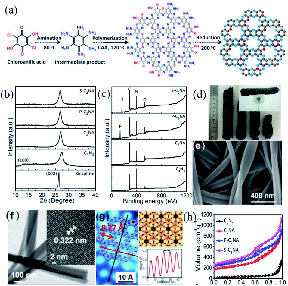 | ||
| Fig. 4 (a) Schematic illustration depicting the development of the S-C2NA, (b) XRD patterns of graphite, and the pristine C3N4, C2NA, P-C2NA, and S-C2NA, and (c) survey scans of the XPS spectra of pristine C3N4, C2NA, P-C2NA, and S-C2NA. (d) Optical image of the fabricated S-C2NA; the inset shows the ultralight aerogel suspended on a dandelion, (e) SEM image of S-C2NA, (f) TEM images of the S-C2NA (inset shows the HRTEM image), and (g) atomic-resolution inverted STM image of S-C2NA on Cu (111). Inset shows the superimposition of the S-C2NA structure (left), atom positions (top-right), and the topographic height profile along the dark red line (down-right). (h) N2 adsorption–desorption isotherms of C3N4, C2NA, P-C2NA, and S-C2NA. Reprinted with permission from ref. 19 copyright 2017 American Chemical Society. | ||
As is known, good control over chemical reactions is highly important for tuning the local elemental distribution and structure at the atomic level of nanomaterials. In this context, Fechler and co-workers24 proposed a eutectic synthesis approach using precursors containing pre-organized nitrogen atoms to realize a controlled polycondensation process instead of a spontaneous process for achieving 2D C2N nanocrystals (Fig. 5a–c). A supramolecular pre-organized mixture of cyclohexanehexone and urea was adopted as precursors, in which the former served as the structure donating motif and the latter could reduce the melting point of the mixture and also provided a nitrogen source. Through a controlled condensation–polymerization reaction and a carbonization process at suitable temperature, graphene-like 2D C2N with a stoichiometric ratio of 2![[thin space (1/6-em)]](https://www.rsc.org/images/entities/char_2009.gif) :1 was fabricated. Based on this approach, other pre-organized precursors were also employed to synthesize graphene-like C2N with a stoichiometric C/N ratio of 2:1, but yet disordered. For instance, Jordan et al.25 successfully prepared laminar C2N crystals starting from squaric acid and urea (Fig. 5d–f). Recently, Walczak et al.9b and Li et al.26 reported the synthesis of porous C2N materials (SSA > 600 m2 g−1) via carbonizing a hexaazatriphenylene precursor at 550 °C while the resultant C2N (C-HAT-CN-550) was rather thick and disorganized (Fig. 5g and h).
:1 was fabricated. Based on this approach, other pre-organized precursors were also employed to synthesize graphene-like C2N with a stoichiometric C/N ratio of 2:1, but yet disordered. For instance, Jordan et al.25 successfully prepared laminar C2N crystals starting from squaric acid and urea (Fig. 5d–f). Recently, Walczak et al.9b and Li et al.26 reported the synthesis of porous C2N materials (SSA > 600 m2 g−1) via carbonizing a hexaazatriphenylene precursor at 550 °C while the resultant C2N (C-HAT-CN-550) was rather thick and disorganized (Fig. 5g and h).
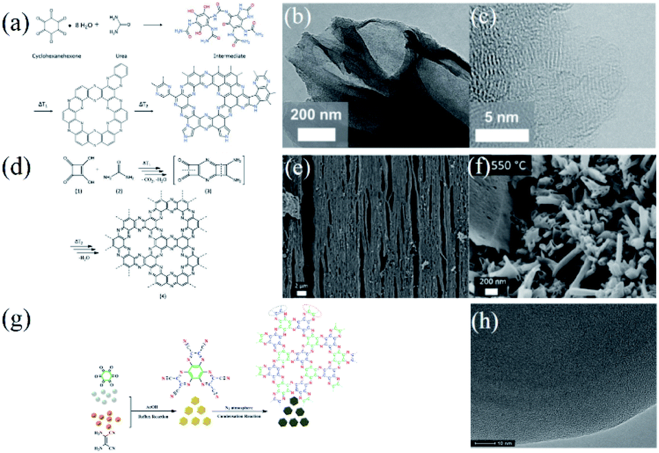 | ||
| Fig. 5 (a) Reaction process scheme of C2N by Fechler et al. (cyclohexanehexone reacted with urea reactants to produce a cross-linked intermediate, which was then converted stepwise to nitrogen functionalized carbons containing primarily pyridinic and pyrazinic nitrogens at temperatures above 500 °C (T1 < T2)) and (b) SEM and (c) TEM images of the resultant product. (a–c) Reprinted with permission from ref. 24 copyright 2015 Wiley-VCH Verlag GmbH & Co. KGaA, Weinheim. (d) Reaction process scheme of C2N by Jordan et al. (squaric acid (1) reacted with urea (2), heated to form squaramide (3) by transamidation and squaramide was then converted into a C2N material (4) via condensation and ring rearrangement at elevated temperature (T1 < T2)). (e and f) SEM images of the primary supramolecular crystals formed from squaric acid (SA) and urea (U) in a ratio of (a and c) 1:1 (SA/U-1) and (b and d) 1:2 (SA/U-2), respectively. The two kinds of complex were treated after thermal condensation of 550 °C. (d–f) Reprinted with permission from ref. 25 copyright 2016 Curtin University of Technology and John Wiley & Sons, Ltd. (g) Reaction progress of porous CN materials by Li et al. (h) TEM image of the resultant product. (g and h) Reprinted with permission from ref. 26 copyright 2019 Elsevier Ltd. | ||
C2N can be prepared by wet-chemical methods9a,19 and solid phase methods.9b,24–26 Compared to the solid phase method, the synthetic procedure of the wet-chemical method is more complex, and the reaction process of the wet-chemical method is more difficult to control. In addition, with different precursors and reaction conditions, the synthesized C2N can have different morphologies, including nanosheets,13 aerogels,27 zeolite-like,26 shale-like and hollow-tube.25 Accordingly, these products possess distinct structural characteristics and physicochemical properties with respect to SSA, defective level, carrier mobility, etc., which enable them to be applied in different fields.
2.3 Electronic properties of C2N
Baek et al. examined the electronic properties of C2N-h2D crystals by fabricating C2N-h2D-based FET devices.9a The semiconducting character of C2N-h2D crystals was validated and a maximum on/off current ratio of 4.6 × 10⁷ was observed with the electron mobility and hole mobility of 13.5 cm2 V−1 s−1 and 20.6 cm2 V−1 s−1, respectively. Moreover, the bandgap was determined to be 1.96 eV, which is close to the value derived from DFT calculations (1.70 eV). Compared to g-C3N4 (2.7 eV),15a the narrower bandgap of C2N-h2D crystals provides them with better visible light absorption, which is beneficial to their photocatalytic applications. Similar to other 2D semiconducting materials, the bandgap of C2N also varies with the crystal thickness. Unfortunately, most of the relevant research studies are theoretically conducted without support from experimental evidence. For instance, Zhang et al. performed a first principles study on the electronic properties of few-layer C2N-h2D crystals with DFT calculations.35 The authors reported that the band structure, especially splitting of the bands, and bandgap of this system depend on the stacking order between the layers, whereas the bandgap exhibits a monotonically decreasing behavior as the layer number increases. A recent theoretical study suggested that the direct bandgap of C2N-h2D can be decreased by 34% with the evolution of structure from monolayer to bulk.36 Therefore, these studies offer a strategy to modulate the bandgap of C2N from the near-infrared to green visible wavelength by controlling the stacking order and layer number of the crystal.The electronic properties of C2N can also be modulated by doping with metal and non-metal elements (e.g. Fe, Co, Ga, Au, F, Cl, Si, Ge, P and As)27–30 based on diverse computational studies. For example, Ma et al.34 theoretically investigated the atomic configurations and electrical properties of C2N monolayers embedded with a single atom of V, Cr and Mn. The local-density-of-states indicated that all three composites show a non-bandgap feature, similar to that of conductors. Du et al.30 reported that the Fermi level of C2N increased and the bandgap decreased with the increase of P/As doping concentration.
Additionally, combining C2N with another semiconductor (e.g. GaTe,31 C3B,32 g-C3N4,33 BCN38) to construct a heterojunction is also a feasible option to modulate the electronic properties of C2N. For example, the bandgap of C2N can be tuned from direct to indirect by forming a monolayer C2N/GaTe heterostructure, as suggested by the calculation results of Bai et al.31 Moreover, the recombination of charge carriers in C2N can be suppressed due to the formation of a built-in electric field in the heterojunction, which is desirable for its applications in optoelectronic devices and photocatalysis.
In summary, engineering the electronic properties of C2N can be realized by thickness control, elemental doping and construction of heterostructures. For elemental doping, both the metal and non-metal dopants can modify the Fermi level and reduce the bandgap of C2N, while the metal doping can significantly narrow the bandgap even down to zero, which makes the metal-doped C2N not suitable for photocatalysis but as an electrocatalyst. Non-metal doping and constructing heterojunctions are effective strategies to modulate the band structure of C2N while maintaining its semiconducting nature. Especially for heterostructured C2N-based composites, both the light absorption and electron–hole pair separation efficiency are improved, making them appealing photocatalysts. The current theoretical progress on the electronic properties of C2N has guiding significance for promoting its practical applications in areas like electronics, catalysis, and photocatalysis.
2.4 Applications of C2N
With the intrinsic semiconducting properties and tunable electronic structure, C2N holds great potential in photocatalysis. Therefore, many studies have demonstrated the photocatalytic performance of C2N and C2N-based materials in different reactions. Meanwhile, the 2D planar and nanoporous structure of C2N make it an outstanding support for loading metal atoms to obtain metal@C2N composite catalysts for various reactions. Especially, the edge N atoms in the nanopores of C2N can effectively trap metal atoms, promoting the bonding between the metals and support. Furthermore, the nanoporosity of C2N also makes it an efficient adsorbent for various gases. Overall, an increasing interest has been focused on the applications of C2N-based materials in different areas.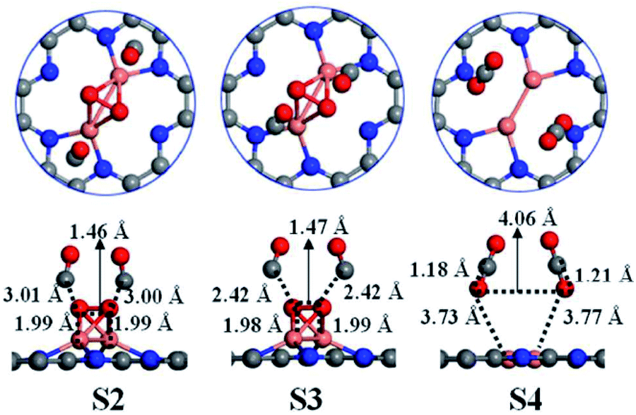 | ||
| Fig. 6 Atomic configurations of S2–S4 and the key structural parameters for CO oxidation via the T-E–R mechanism on Cu2@C2N. Color scheme: C, gray; N, blue; O, red; Cu, orange. Reprinted with permission from ref. 16b, copyright 2018 The Royal Society of Chemistry. | ||
The width of the pores in C2N is estimated to be 3.0 Å, smaller than that of O2, N2, CO, and CO2, but larger than the kinetic diameter of H2 (2.89 Å) and He (2.6 Å).49f Thus, C2N may serve as a promising H2 and He gas separation membrane material. In addition, the unique porous structure of C2N also makes it a potential adsorbent for gases like H2, CO2 and VOCs. Hashmi et al.49b explored the H2 adsorption of C2N and Li decorated C2N using the DFT method, and found that the Li decoration significantly improved H2 adsorption on C2N. A theoretical gravimetric density of 13 wt% was reached for Li decorated C2N, which is much higher than that reported for other 2D materials decorated with alkali metals. Walczak and co-workers49d reported that CO2 adsorption uptake of the prepared C2N sample (C-HAT-CN-550) reached a high value of 3.24 mmol g−1 (at 273 K and p = 0.15 bar). Lu's group28 theoretically studied CO2 capture properties on metal-embedded C2N. Incorporation of open metal sites into the C2N framework can enhance the bonding of CO2 on the adsorbent along with low-temperature desorption capacity. The authors screened a series of metal-embedded C2N including Ca and the early 3d TMs as CO2 adsorbents and found that Ca-embedded C2N shows the most promising reversible CO2 capture performance. From DFT calculations, Ao et al.49e found that pure C2N can adsorb some typical VOCs like formaldehyde, benzene and trichloroethylene. Moreover, the adsorption ability of C2N can be improved by Al doping. In their later study, the Al-doped C2N was found to co-adsorb H2O and O2, implying the possible generation of hydroxyl and superoxide radicals, showing promising applications for VOC degradation as the hydroxyl and superoxide radicals are highly oxidizing species.50
Besides the aforementioned applications, Xu and co-workers also applied C2N as an electrode material for lithium-ion batteries (LIBs) and a high initial discharge capacity and high stability of C2N-based LIBs were observed.13a
2.5 Summary of C2N
Thanks to the efforts of Baek and co-workers, the 2D C2N crystal has attracted wide attention in the last five years, due to its high stability, hole structure, high SSA, and other physical and chemical properties. Although there are several methods to synthesize C2N, the complex synthesis process and the expensive and rare precursors limit its large-scale production and practical applications. Therefore, it is urgent to develop low-cost and easy-operation methods to fabricate the 2D C2N crystal. As a kind of semiconductor, the 2D C2N crystal has a tunable bandgap, high carrier mobility, and special porous structure, which enable it to perform well in areas like FET,9a HER23 and LIBs.13a In addition, based on DFT calculations, researchers reported the promising use of 2D C2N materials in the OER,42 CO oxidation,34 CO2RR,27 NRR,48 and gas adsorption.49 Moreover, Mahmood et al.9a predicted that C2N could be used in electrodes for energy storage, gas storage and some other areas. The applications of C2N are summarized in Fig. 7.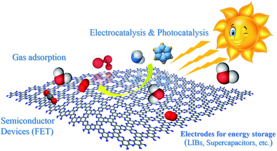 | ||
| Fig. 7 Potential applications of the C2N-h2D crystals. | ||
3. C3N
The possible crystal structure of 2D C3N was predicted as an indirect-bandgap semiconductor a few decades ago and it aroused much interest from the scientific community.51 Therefore, a considerable amount of effort on its synthesis was attempted, but to achieve amorphous products in a C3N stoichiometry without a 2D structure, which could not testify the theoretical calculations.52 Until 2016, Baek and co-workers13a,53 successfully synthesized a 2D layered C3N nanocrystal, whose structure was in good agreement with the predictions. Then, this new member of the 2D CxNy family has been widely applied as a catalyst, electrode material, and adsorbent, due to its peculiar electrical and chemical properties.3.1 Crystalline Structure of C3N
A C3N monolayer can be regarded as a N-doped graphene structure, where the molar ratio of C to N is 3:1 and all the N atoms belong to graphitic N. Similar to graphene, the atoms in C3N also exhibit sp2 hybridization.54 Apparently, the C3N framework is quite different from the C2N framework, where periodic holes are not included. The monolayer C3N has a lattice parameter of 4.863 Å, with the C–N bond length of 1.403 Å and the C–C bond length of 1.404 Å.
3.2 Synthesis of C3N
Compared to C2N, there are less available methods for the synthesis of C3N. King et al.55 obtained a mixture of amorphous C3N flakes with a thickness of 1–3 μm and graphitic carbon microspheres through annealing a nitrogen-rich polymer precursor (m-phenylenediamine) in a vacuum-sealed quartz tube at 800 °C for 7–9 days. To improve the crystallinity of C3N, Baek and co-workers13a,53 then used organic hexaaminobenzene trihydrochloride (HAB, C6N6H15Cl3) crystals as precursors and successfully obtained 2D layered C3N nanocrystals by decomposing the HAB into C6N2, NH4Cl, and NH3 at 500 °C for 2 h under an argon atmosphere (Fig. 8a). The resultant C3N nanocrystal is multilayered and represents a similar hexagonal morphology to the HAB crystals.53 The interlayer distance of the as-prepared C3N nanocrystal is estimated to be 3.40 Å according to the XRD characteristic peak at 2θ of 26.12° (Fig. 8b). In addition, another two major peaks at 2θ of 12.8° and 44.7° are also present in the XRD pattern. Meanwhile, the authors confirmed the C3N chemical composition, molecular structure and bond nature of the as-prepared nanocrystal via XPS (Fig. 8c).53 Furthermore, the 2D C3N framework at the atomic level was unambiguously illustrated with the assistance of the STM method and the dot-to-dot distance in the well-ordered triangular structure of C3N was found to be 442 ± 16 pm, which was in good match with the DFT modelling (Fig. 8e).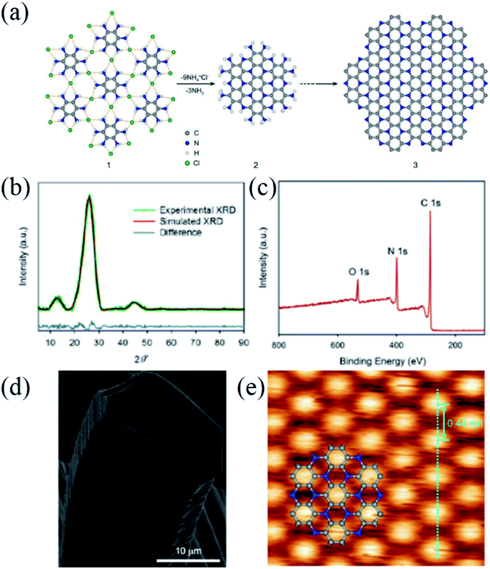 | ||
| Fig. 8 (a) Schematic representation of C3N, (b) experimental PXRD pattern from C3N (dark green), simulated XRD after Pawley refinement (dark red) and the difference (dark blue), (c) XPS survey spectrum of C3N, (d) SEM image of C3N, and (e) STM image of a 2D PANI framework (2.5 × 2.5 nm2, Vs. = −1.1 V, It = 1.0 nA). Inset structure represents C3N repeating units with carbon atoms (gray balls) and nitrogen atoms (blue balls). Reprinted with permission from ref. 53 copyright 2016 National Academy of Sciences. | ||
Recently, fabrication of C3N quantum dots (QDs) was reported by Yang et al.13b In their work, a precursor of 2,3-diaminophenazine (DAP) is polymerized by a typical hydrothermal method, forming C3N QDs and C3N nanosheets (Fig. 9a). The layered C3N was formed at a DAP concentration of 0.8 mM and 250 °C. Especially, by prolonging the polymerization reaction time to 200 h, 2D C3N nanocrystals containing a high proportion of large, single-layer and single crystalline nanosheets can be obtained (Fig. 9b and c). For QDs, the size can be controlled in the range of 1.8–5.5 nm by varying the concentration of DAP solution and hydrothermal temperature (Fig. 9d and e).
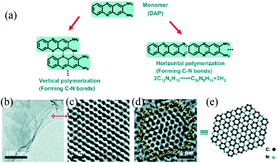 | ||
| Fig. 9 (a) Schematic of the vertical and horizontal polymerization of DAP forming C–N bonds. The polymerization advances via abstraction of H from C–H and N–H bonds followed by formation of C–N bonds. (b) TEM image of a mixture of single- and multilayer C3N sheets, (c) spherical aberration-corrected HRTEM image showing the honeycomb structure of a single-layer sheet marked in (b), and (d) spherical aberration-corrected HRTEM image of a single C3N QD with a C–N zigzag edged structure. The yellow balls represent the carbon and nitrogen atoms on the edge, while the red sticks represent the chemical bonds between atoms on the edge. (e) The molecular structure scheme of the C3N QD in (d). Reprinted with permission from ref. 13b copyright 2017 Wiley-VCH Verlag GmbH & Co. KGaA, Weinheim. | ||
3.3 Electronic properties of C3N
C3N is an indirect bandgap semiconductor with the valence and conduction bands located at the M and Γ points, respectively.56 Determination of the theoretical bandgap of a C3N monolayer is still debatable since different computation software gives discrepant values while convincing experimental evidence is not available thus far.51b,54 For instance, Zhou et al.56a derived a bandgap of 1.04 and 0.39 eV for a C3N monolayer by using HSE06 software and the generalized gradient approximation (GGA) method, respectively.Experimentally, Mahmood et al.53 measured the bandgap of an as-prepared 2D C3N framework to be 2.67 eV by using a lock-in detection technique with scanning tunnelling spectroscopy and electrochemical methods. This result is far away from the theoretical value, possibly because the thickness can affect the bandgap of C3N nanocrystals. Surprisingly, Mahmood and co-workers found that doping the as-prepared multilayered C3N with HCl could remarkably reduce its bandgap since the conductivity was improved from 0.72 ± 0.04 S cm−1 (undoped) to 1.41 × 10³ S cm−1 (doped). In fact, the HCl-doped 2D C3N almost behaves as a conductor, which is more coincident with the calculations.
Yang et al.13b measured the bandgap of C3N QDs based on ultraviolet photoelectron spectroscopy and UV-vis spectroscopy. It was found that the bandgap value of C3N QDs decreases with increasing diameters of the QDs, e.g., the bandgap varies from 2.74 to 0.39 eV with the size of QDs ranging from 1.8 to 30 nm. A further increase of the QD size larger than 30 nm barely affects the bandgap. Such a feature of size-dependent bandgaps provides C3N QDs with tunable photoluminescence, favoring their applications in bioimaging. Notably, the unique bandgap structure of C3N QDs also enables them to have a much higher quantum yield and life-time than graphene QDs. In addition, Yang et al.13b also investigated the electrical properties of a monolayer C3N nanosheet with FET devices. The average ION/IOFF ratio for the C3N-based FETs reached 5.5 × 10¹⁰ and the hole and electron mobilities of the C3N monolayer were measured to be 1.2 and 1.5 cm2 V−1 s−1 respectively. Notably, the ION/IOFF ratio of C3N is three orders of magnitude higher while the carrier mobility is lower than that of C2N-h2D crystals. Interestingly, theoretical calculations reported that the carrier mobility of C3N is anisotropic and the hole mobility along the armchair direction of the C3N monolayer can reach up to 1.08 × 104 cm2 V−1 s−1, much higher than that of C2N-h2D crystals.56b These results demonstrate that the intrinsic conductivity and carrier mobility of C3N are better than those of C2N, indicative of the promising applications of C3N in FET devices and electrode materials. The hole and electron mobility of C3N could be further improved to 180 and 220 cm2 V−1 s−1, respectively, by hydrogenation in H2, while the intrinsic mechanism is unknown yet. Interestingly, the hydrogenated C3N nanosheet even exhibits a ferromagnetic state according to both the DFT calculations and magnetic performance measurements.
Several theoretical studies demonstrated that the electronic properties of C3N can also be modulated by forming heterojunctions with another semiconductor (e.g. g-C3N4,57 C3B58). Due to the narrow bandgap and good carrier mobility of C3N, it can act as a photosensitizer to enhance the visible light absorption and also retard the charge recombination of the heterostructure, which can improve the photocatalytic activity.
3.4 Application of C3N
As a semiconductor with a small bandgap, C3N shows a broadband solar light absorption, which indicates its potential utilization in photocatalysis. Meanwhile, because of the structural similarity to N-doped graphene which exhibits good electrocatalytic activities for reactions like the ORR, HER, etc., the potential application of C3N in electrocatalysis was investigated. Furthermore, C3N is also considered as a promising electrode material for batteries and as a gas adsorbent owing to its peculiar electrical properties and planar structure. The applications of C3N in photocatalysis, electrocatalysis, batteries and gas adsorption are summarized in this section.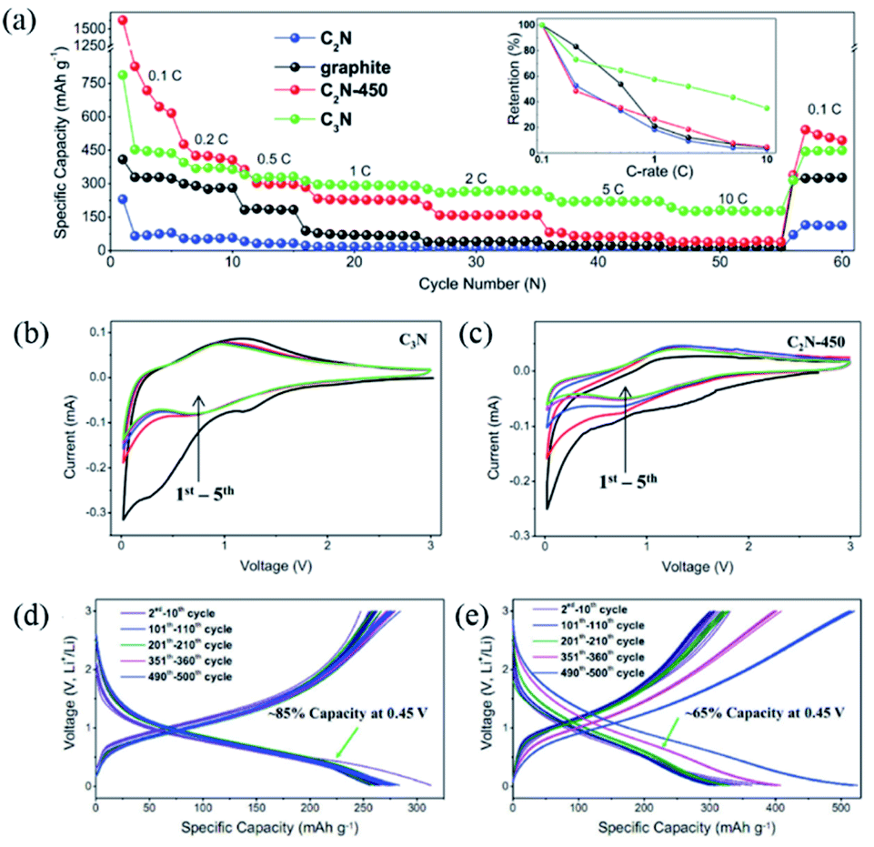 | ||
| Fig. 10 (a) Rate capability measurements for C2N, C2N-450, C3N, and graphite at various C-rates from 0.1 to 10C. Representative cyclic voltammograms of (b) C3N and (c) C2N-450 for the five cycles at a scan rate of 0.1 mV s−1. Charge/discharge profiles of (d) C3N and (e) C2N-450 at 1C. Reprinted with permission from ref. 13a copyright 2017 Wiley-VCH Verlag GmbH & Co. KGaA, Weinheim. | ||
In the above work,13a a significant capacity loss in the first several cycles was witnessed (Fig. 10a), which limits its application in LIBs. Liu and co-workers60 performed first-principles simulations on the intercalation process of Li ions into C3N and suggested that the behavior is a result of N excess C3N (C2.67N) in Xu's experiment.13a With the N excess in the C3N framework, N-doping and carbon-vacancy defects are present, which strengthen the intercalation of Li ions into C2.67N and the energy barriers of the deintercalation process. It was proposed that C3.27N maintained high reversible capacity in LIBs. Later, Preeti et al.61 demonstrated that the C3N monolayer also serves as a promising anode material for Na/K-ion batteries with a storage capacity of up to 1072 mA h g−1via first-principles calculations.
Gas adsorption capacities of the C3N monolayer were found to be improved by doping with inorganic or metal elements. Pashangpour and Peyghan65 assessed the adsorption of CO onto B-doped and Al-doped C3N nanosheets by DFT calculations. The introduction of B dopants barely promoted the weak physisorption of CO onto the pristine C3N nanosheet, whereas the Al doping significantly enhanced the interaction between CO and C3N nanosheets. Moreover, CO adsorption onto the Al-doped C3N nanosheet induces noticeable changes of electrical conductivity of the sheet. These findings implied the potential application of Al-doped C3N nanosheets as both the CO adsorbent and sensors. Recently, several computational studies demonstrated the excellently reversible CO2 capture capacity on the negatively polarized C3N monolayer.66 It was shown that the negative polarization could turn the physisorption of CO2 into chemisorption. In addition, the negatively charged C3N monolayer was a promising material to separate CO2 from the mixtures of CO2/N2, CO2/H2, CO2/CH4, and CO2/C2H2, and to separate C2H2 from the mixtures of C2H2/CH4 and C2H2/H2 through manipulating the negative charge density.66b
Multilayered C3N crystals are also reported to be highly efficient for gas adsorption,67 similar to multilayered graphene.68 Li et al.16a constructed a periodic 3D pore model containing two C3N monolayers (denoted as C3N pores) with a pore size of 0.75 nm (Fig. 11a) and showed that the C3N pores manifest an extremely high CO2 adsorption capacity up to 3.99 mmol g−1 in air at 23 °C. Moreover, the C3N pores show preferential adsorption of CO2 over CO, H2, and CH4 and the CO2 selectivity could be further boosted by regulating the size of C3N pores from 0.75 to 0.65 nm (Fig. 11b–d). The high selectivities in CO2/CO, CO2/H2, and CO2/CH4 are ascribed to the larger polarizability and quadrupole moment of CO2 molecules than the other three gas molecules, which enables stronger interaction between CO2 molecules and the C3N surface. Furthermore, the strong interaction between CO2 molecules and the C3N surface causes the CO2 adsorption to slightly decrease in the presence of water (3.80 mmol g−1). Recently, Ma et al.69 used ZIF-8 and urea as precursors to synthesize C3N-type N-rich carbon layers and applied them in methanol adsorption. A sample (CN950) with a SSA of 1496 m2 g−1 reached the highest methanol adsorption capacity of 13.2 mmol g−1.
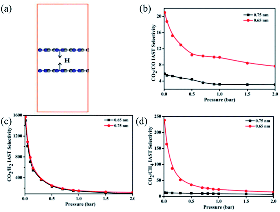 | ||
| Fig. 11 (a) Molecular model of C3N pores with a pore size of 0.75 nm. (b) CO2/CO, (c) CO2/H2, and (d) CO2/CH4 selectivity of C3N pores with different pore sizes versus the adsorption pressure at 23 °C. Reprinted with permission from ref. 16a copyright 2017 American Chemical Society. | ||
3.5 Summary of C3N
C3N has a graphene-like crystalline structure, good chemical stability and an indirect bandgap, enabling plentiful applications in electronics, photocatalysis, electrocatalysis, energy storage devices, and gas adsorption. Multilayered C3N can be synthesized via a carbonization process of precursors containing C and N, which is much simpler than that for C2N layers. However, available methods for preparing single-layered or few-layered C3N nanosheets and controllable modifications of C3N are quite limited. Due to the much narrower bandgap than that of the C2N monolayer, the C3N monolayer itself possesses limited photocatalytic activity and it usually combines with other wide-bandgap semiconductors to form heterojunctions for photocatalysis. However, the better electrical conductivity and chemical stability of C3N than C2N enables it to have more promising applications in LIBs. In addition, the electrocatalytic activity of C3N can be improved by rational chemical modifications. Furthermore, the gas adsorption capacity of C3N can be tailored by doping, polarization and regulation of C3N pores, making it a good candidate for a gas adsorbent. Definitely, the physicochemical and structural characteristics of C3N are not fully understood thus far and there are still many potential applications for C3N in the areas of environment and energy (as shown in Fig. 12). It is hoped that more efforts will be devoted to advance our knowledge in C3N.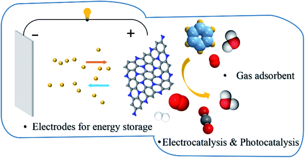 | ||
| Fig. 12 Potential applications of C3N. | ||
4 Graphite-like CN (g-CN)
The presence of g-CN nanocrystals has been reported for a long time, but little progress on its synthesis and applications has been made. In 2006, Cao et al.70 proposed a simple solvothermal approach with cyanuric chloride and sodium precursors to obtain 1D CN nanostructures, which involves an initial formation of graphite-like carbon nitride (g-CN) layers followed by self-assembly into tubes, ribbons or microspheres (Fig. 13a–c). So far, the successful preparation of CN is absent in the literature. On the other hand, many theoretical studies have been conducted on the properties and potential applications of g-CN.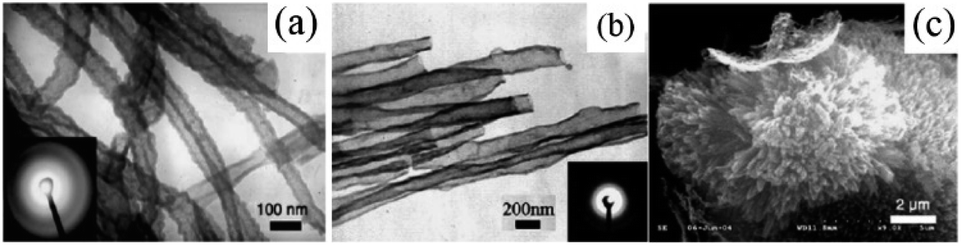 | ||
| Fig. 13 (a) TEM image of a bundle of g-CN nanotubes and the embedded SAED, (b) TEM image of a bundle of g-CN nanoribbons (SAED embedded), and (c) SEM image of g-CN microspheres, reprinted with permission from ref. 70 copyright 2006 Elsevier Ltd. | ||
4.1 Crystalline structure of g-CN
The g-CN monolayer structure is composed of uniform holes and aromatic benzene rings containing three N atoms and three C atoms alternatively arranged in the ring (Fig. 1).71 The benzene rings are bridged by C–C bonds to form nanopores in g-CN, and all the N atoms belong to pyridine N. The lattice parameter is derived to be 7.12 Å, and the bond lengths of C–C and C–N are estimated to be 1.51 and 1.34 Å, respectively.4.2 Electronic properties of g-CN
g-CN is predicted to behave as a semiconductor. To calculate the bandgap of the g-CN monolayer, Srinivasu et al.72 used different methods and obtained different values. They stated that 2.89 eV should be more plausible based on Cao's work,70 which observed broad photoluminescence peaks at 430–450 nm (corresponding to a bandgap of ∼2.73 eV) for the as-prepared g-CN nanotubes, nanoribbons and microspheres. Unluckily, experimental measurements in the bandgap of 2D g-CN crystals are unavailable yet. Meanwhile, Srinivasu et al.72b also studied the bandgap of multilayered g-CN and suggested that the bandgap decreased gradually from 2.89 to 2.72 eV with the layer number in the range of 1–6, which originates from the interlayer coupling. Furthermore, they found that doping the g-CN monolayer with phosphorus atoms (P@g-CN) could further reduce its bandgap to 2.31 eV, which corresponds to an appreciable visible light, whereas boron, oxygen and sulfur dopants are less efficient. Recently, Li et al.41 reported that embedding a TM atom (TM = Pt, Pd, Co, Ni and Cu) into the g-CN framework could transform g-CN from a direct bandgap into an indirect bandgap with values of 0.41–0.52 eV. With the maneuverable band structure, g-CN is also expected to show great potential in photocatalysis.4.3 Applications of g-CN
Unlike C2N and C3N, only a few examples of the applications of g-CN have been presented from computations in the literature. For instance, Srinivasu et al.72b evaluated the potential of g-CN, B@g-CN and P@g-CN for photocatalytic water splitting. P@g-CN is supposed to exhibit the best HER performance under visible light among the three samples due to its smaller bandgap, suitable conduction band minimum (CBM) position above the water oxidation potential and valence band minimum (VBM) position below the water reduction (Fig. 14a). In addition, the similar nanoporosity of g-CN to that of the C2N framework also makes it an excellent support of SACs for various reactions because the sp2-hybridized N atoms at the vacancy hole edges can afford coordination sites to anchor the metal atoms. In this regard, Li et al.41 designed a series of g-CN supported TM (TM = Pt, Pd, Co, Ni and Cu) SACs and studied their OER performances by DFT calculations (Fig. 14b). The computational results displayed that all the TM@CN materials function as good electrocatalysts for the OER and Co@CN is the most ideal one due to its lowest overpotential of ∼0.16 V. Although the TM@g-CN materials are not efficient to drive the water splitting under visible light irradiation due to their narrow bandgap (0.41–0.52 eV), the stable Pd-(OH)2@g-CN complex with modified band structure exhibits a promising photocatalytic activity for visible-light-driven OER. Recently, Chen et al.71 demonstrated that a Li decorated g-CN monolayer presents a high efficiency in hydrogen storage systems, because of sufficient adsorption sites for hydrogen molecules. With the high Li loading, the Li decorated g-CN shows a good hydrogen adsorption performance with a theoretical gravimetric density of 10.81 wt%.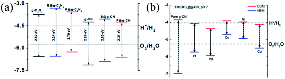 | ||
| Fig. 14 (a) Calculated VBM and CBM positions of g-C3N4 and g-CN along with their boron and phosphorus doped counter parts, reprinted with permission from ref. 72b copyright 2014 American Chemical Society. (b) The energy band alignment of TM–(OH)2@CN. The vacuum level is set at 0 eV, and the chemical reaction potentials for H+/H2 and O2/H2O are plotted with dotted lines. Reprinted with permission from ref. 41 copyright 2016 The Royal Society of Chemistry. | ||
5. Other CxNy
Besides the aforementioned 2D CxNy structures, several other 2D CxNy compounds with different stoichiometries including C2N2, C2N3, C5N, and C5N2 have also been reported in the literature, while less attention has been focused on them. Hence, we will give a brief introduction in this section.5.1 Diamond-like CN (c-C2N2) and hexagonal CN (h-C2N2)
Recently, two new types of stable 2D CxNy were predicted by Dong et al.14via the DFT method, c-C2N2 and h-C2N2. It is worth mentioning that the crystalline structures of the two C2N2 materials are quite different from the above typical monolayer-structured CxNy, since there are two atomic layers in the unit cells of c-C2N2 and h-C2N2. As shown in Fig. 15, both of them are constituted by two g-CN layers connected with C–C bonds, while the stacking modes of the layers are different. As a result, C atoms exhibit sp3 hybridization and N atoms are sp2 hybridized in both the c-C2N2 and h-C2N2 frameworks. According to the calculation results, c-C2N2 and h-C2N2 are wide-band semiconductors with the bandgaps of 4.43 and 3.70 eV, respectively. Meanwhile, good mechanical strength and high thermal conductivity of the two CxNy are also predicted. Unfortunately, the synthesis of the two structures has not been realized yet in the laboratory to provide experimental confirmation.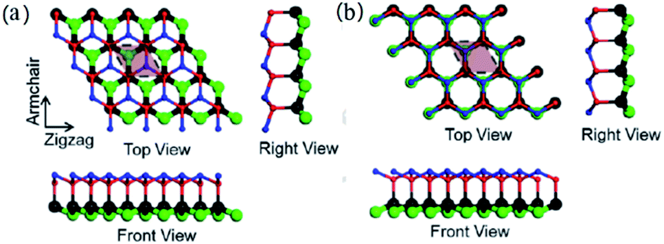 | ||
| Fig. 15 Lattice structures of c-C2N2 (a) and h-C2N2 (b). Carbon atoms are colored with black in the bottom layer and red in the top layer. Nitrogen atoms are colored with green in the bottom layer and blue in the top layer. Reprinted with permission from ref. 14 copyright 2018 Elsevier B.V. | ||
5.2 C2N3
Recently, Shi et al.73 firstly studied the structural characteristics of C2N3 and its structural stability and strain behavior by DFT calculations. The C2N3 monolayer is a kind of carbon nitride with a C/N ratio of 2/3, which has the calculated lattice contents of a = 7.846 Å and c = 6.549 Å with a P6/mcm space group (Fig. 1). The bond lengths are 1.366 Å, 1.360 Å, and 1.340 Å for the N(1)–C(1), N(2)–C(1) and N(3)–C(1), respectively. The C2N3 monolayer exhibits a typical p-type semiconductor behavior and good structural stability with Poisson's ratios of 0.39 and 0.27 in zigzag and armchair forms, respectively.5.3 C5N
Wu et al.74 used the ab initio evolutionary algorithm method to calculate four kinds of thermodynamically stable C5N phases (P62m (Fig. 1), R3m![[1 with combining macron]](https://www.rsc.org/images/entities/char_0031_0304.gif) , R3m
, R3m![[2 with combining macron]](https://www.rsc.org/images/entities/char_0032_0304.gif) and C2/m). To explore the stability of the new phases, they carried out simulations under a high pressure of 100 GPa and the mechanical properties and evaluated the hardness of these phases. Moreover, the electronic properties, energy bandgap and band structure of the C5N were calculated. R3m, R3m and C2/m phases are semiconducting with the bandgaps of 5, 5 and 2.15 eV, respectively, while P62m shows a metallic character.
and C2/m). To explore the stability of the new phases, they carried out simulations under a high pressure of 100 GPa and the mechanical properties and evaluated the hardness of these phases. Moreover, the electronic properties, energy bandgap and band structure of the C5N were calculated. R3m, R3m and C2/m phases are semiconducting with the bandgaps of 5, 5 and 2.15 eV, respectively, while P62m shows a metallic character.
5.4 C5N2
The C5N2 monolayer has a similar porous crystalline structure to the C2N monolayer, except that the primitive cell of the C5N2 is constituted by five fused benzene-like rings (three fused rings for C2N) bridged by pyrazine N (Fig. 16).75 Accordingly, the primitive cell of C5N2 contains 30 C atoms and 12 N atoms (CN stoichiometric ratio of 5:2) and the optimized lattice parameter and the pore diameter are derived to be 16.59 Å and 11.52 Å, respectively, larger than those of C2N.75 Due to the nanoporosity of C5N2, it is also called holey C5N2 (h-C5N2). Theoretical calculations suggested that C5N2 is also a semiconductor and that the bandgap of a C5N2 monolayer is computed to be 1.10 eV, lower than that of a C2N monolayer (1.72 eV).76
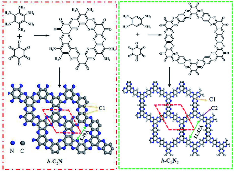 | ||
| Fig. 16 Schematic representation of the synthesis of C2N and C5N2 and graphic representation of a one-layer-conjugated skeleton. Reprinted with permission from ref. 75 copyright 2019 Elsevier B.V. | ||
Very recently, the successful preparation of 2D multilayered C5N2 was reported by Kim et al.77 In their work, 1,2,4,5-benzenetetramine and hexaketocyclohexane were used as precursors. An efficient reversible imine condensation reaction was triggered by exposing the mixture under simulated sunlight irradiation for 3 h. Meanwhile, the electrical property measurement on the pellet of as-prepared 2D C5N2 crystals showed that 2D C5N2 crystals are semiconducting with a conductivity of 2.22 × 10⁻³ S m−1. Furthermore, the 2D C5N2 film was observed to exhibit a rapid photo-response to white light irradiation, suggesting its potential in photocatalysis.
6. Summary and outlook
Over the last few years, 2D CxNy nanocrystals have attracted great interest arising from their graphene-like structure, open bandgap, large SSA, good chemical stability, and tunable surface chemistry, which enable plentiful applications in the areas of electronics, photocatalysis, electrocatalysis, energy storage devices, and gas adsorption/separation. In the 2D CxNy family, C2N, C3N and C5N2 have been successfully synthesized, while the other members including g-CN, c-C2N2, h-C2N2 and C5N are only theoretically predicted thus far. Among them, C2N has been mostly studied because of its suitable bandgap and unique nanoporous structure, which make it a potential photocatalyst, catalyst support for SACs and double-atom catalysts and membrane materials.79 With the semiconducting electronic properties, face termination for electron localization, high SSA, 2D CxNy almost possess all the prerequisites as nonmetal heterogeneous catalysts. Additionally, the abundantly distributed Lewis basic functions and Brönsted basic functions originating from the electronegativity differences between N and C atoms in the CxNy framework can serve as catalytic sites for diverse reactions. In fact, g-C3N4 has already been reported to be an excellent metal-free catalyst for organic reactions and cyclisation of functional nitriles.80 Thereby, 2D CxNy materials are also promising metal-free heterogeneous catalysts and relevant studies deserve to be conducted in future. Hence, a vast amount of efforts has been devoted to the applications of C2N in photocatalytic water splitting, multiple electrocatalytic reactions involving the ORR, HER, CO2RR, and NRR, as well as gas adsorption/separation. Compared to C2N, C3N possesses a narrower bandgap but better electronic conductivity, which makes C3N promising for not only photocatalysis and electrocatalysis but also battery electrodes. As for g-CN, c-C2N2, h-C2N2, C5N and C5N2, their possible applications are rather limited in the literature. A summary of the physicochemical properties, synthesis methods and potential applications of 2D CxNy is presented in Table 1. Albeit with the considerable progress on 2D CNs, there are still challenges that should be addressed in further work:| CxNy | Bandgap/eV | Hole size/Å | Synthesis methods | Potential applications | Ref. |
|---|---|---|---|---|---|
| a —: unknown. | |||||
| g-C3N4 | 2.70 | 6.8 | Thermal reactionsSolvothermal reactionsChemical vapor depositionSol–gel synthesisMicrowave heating | Water splittingCO2 reductionOrganic contaminant purificationFuel cells | 15a and 78 |
| g-CN | 2.73 | — | Solvothermal approach | Water splitting | 41 and 72b |
| Hydrogen storage | 71 | ||||
| C2N | 1.96 | 8.3 | Wet-chemical reactionSolid phase methods | Water splitting | 19, 23, 38 and 39–41 |
| CO oxidation | 16b, 34, 39 and 43 | ||||
| CO2RR | 46 and 47 | ||||
| NRR | 48 | ||||
| Gas adsorption/separation | 49 | ||||
| Fuel cells | 13a | ||||
| FET | 9a | ||||
| C3N | 2.67 | Non-holey | Thermal reactionsHydrothermal method | Water splitting | 57 and 58 |
| Fuel cells | 59–61 | ||||
| Gas adsorbent | 62–66 | ||||
| c-C2N2 | 4.43 | Non-holey | — | — | 14 |
| h-C2N2 | 3.70 | Non-holey | — | — | |
| C2N3 | 3.26 | — | — | — | 73 |
| C5N (P62m) | 0 | Non-holey | — | — | 74 |
| C5N2 | 1.1 | 11.52 | Reversible imine condensation reaction | Photocatalysis | 76 and 77 |
(i) The currently used precursors for CxNy synthesis are relatively expensive and some of the available synthetic strategies are complex and require strict experimental conditions, which limit the large-scale production and practical applications. This is also the reason that a majority of the 2D CxNy compounds are theoretically investigated. Consequently, it is urgent to develop low-cost and easy-operation methods to fabricate 2D CxNy crystals.
(ii) Most of the obtained 2D CxNy crystals are in multilayered structure, while the layer number greatly affects the physicochemical properties of CxNy and thus their applications. Hence, preparation of single-layered and few-layered CxNy is of importance.
(iii) Surface modifications like creating defects, functionalizing with oxygenated groups, doping with heteroatoms, etc. are believed to have a vital influence on the electronic and catalytic properties of CxNy, while relevant experimental and theoretical studies are very limited so far. Therefore, rational surface engineering of 2D CxNy should also be paid attention for promoting their practical applications.
(iv) In light of the good gas adsorption/separation efficiency of 2D CxNy for small molecular gases including H2, He, CO, and CO2, adsorption of VOC molecules is more important. Especially, the nanopores in C2N, g-CN and C5N2 may be efficient for VOC separation. Doping CxNy with specific elements or building a composite material can enhance their selective adsorption towards gas molecules. Therefore, further attempts on the potential applications of 2D CxNy in adsorption are very promising.
(v) Since the good performance of C2N- and C3N-based photocatalysts for water splitting and the wide bandgap of g-CN, c-C2N2, h-C2N2, C5N and C5N2 have been theoretically illustrated, 2D CxNy materials are also expected to hold potential in photocatalytic degradation of both aqueous organic pollutants and VOCs for environmental remediation. Moreover, large SSA and planar structures of 2D CxNy can possibly facilitate more exposure of active sites and adsorptive photocatalysis, beneficial to the photocatalytic degradation processes.
In summary, research on various 2D CxNy structures and their potential applications in different fields is still in its infancy. The challenges and various opportunities are huge for the scientific community to explore. We wish that the information provided in this review can attract increasing interest in the area of 2D CxNy.
Conflicts of interest
There are no conflicts to declare.Acknowledgements
Li Tan and Chunyang Nie contributed equally to this work. This work was supported by the National Natural Science Foundation of China (No. 21777033 and 21806024), China Postdoctoral Science Foundation (No. 2017M622637), Science and Technology Planning Project of Guangdong Province (No. 2017B020216003), Innovation Team Project of Guangdong Provincial Department of Education (No. 2017KCXTD012), and Australian Research Council (DP170104264).References
- K. S. Novoselov, A. K. Geim, S. V. Morozov, D. Jiang, Y. Zhang, S. V. Dubonos, I. V. Grigorieva and A. A. Firsov, Science, 2004, 306, 666 CrossRef CAS
.
- X. Du, I. Skachko, A. Barker and E. Y. Andrei, Nat. Nanotechnol., 2008, 3, 491 CrossRef CAS
-
(a) D. Sun, D. Ye, P. Liu, Y. Tang, J. Guo, L. Wang and H. Wang, Adv. Energy Mater., 2018, 8, 1702383 CrossRef
- K. C. Kemp, H. Seema, M. Saleh, N. H. Le, K. Mahesh, V. Chandra and K. S. Kim, Nanoscale, 2013, 5, 3149 RSC
- J. B. Wu, M. L. Lin, X. Cong, H. N. Liu and P. H. Tan, Chem. Soc. Rev., 2018, 47, 1822 RSC
-
(a) M. Terrones, A. R. Botello-Méndez, J. Campos-Delgado, F. López-Urías, Y. I. Vega-Cantú, F. J. Rodríguez-Macías, A. L. Elías, E. Muñoz-Sandoval, A. G. Cano-Márquez and J.-C. Charlier, Nano Today, 2010, 5, 351 CrossRef
-
(a) W. Dacheng, L. Yunqi, W. Yu, Z. Hongliang, H. Liping and Y. Gui, Nano Lett., 2009, 9, 1752 CrossRef
- H. Wang, T. Maiyalagan and X. Wang, ACS Catal., 2012, 2, 781 CrossRef CAS
-
(a) J. Mahmood, E. K. Lee, M. Jung, D. Shin, I. Y. Jeon, S. M. Jung, H. J. Choi, J. M. Seo, S. Y. Bae, S. D. Sohn, N. Park, J. H. Oh, H. J. Shin and J. B. Baek, Nat. Commun., 2015, 6, 6486 CrossRef CAS
- A. Y. Liu and M. L. Cohen, Science, 1989, 245, 841 CrossRef CAS
- X. Wang, K. Maeda, X. Chen, K. Takanabe, K. Domen, Y. Hou, X. Fu and M. Antonietti, J. Am. Chem. Soc., 2009, 131, 1680 CrossRef CAS
-
(a) M. Z. Rahman, K. Davey and C. B. Mullins, Adv. Sci., 2018, 5, 1800820 CrossRef
-
(a) J. Xu, J. Mahmood, Y. Dou, S. Dou, F. Li, L. Dai and J. B. Baek, Adv. Mater., 2017, 29, 1702007 CrossRef
- Y. Dong, C. Zhang, M. Meng, M. M. Groves and J. Lin, Carbon, 2018, 138, 319 CrossRef CAS
-
(a) S. Ye, R. Wang, M.-Z. Wu and Y.-P. Yuan, Appl. Surf. Sci., 2015, 358, 15 CrossRef CAS
-
(a) X. Li, L. Zhu, Q. Xue, X. Chang, C. Ling and W. Xing, ACS Appl. Mater. Interfaces, 2017, 9, 31161 CrossRef CAS
-
(a) O. Y. Podyacheva, D. A. Bulushev, A. N. Suboch, D. A. Svintsitskiy, A. S. Lisitsyn, E. Modin, A. Chuvilin, E. Y. Gerasimov, V. I. Sobolev and V. N. Parmon, ChemSusChem, 2018, 11, 3724 CrossRef CAS
- T. Komatsu and M. Samejima, J. Mater. Chem., 1998, 8, 193 RSC
- S. S. Shinde, C. H. Lee, J. Y. Yu, D. H. Kim, S. U. Lee and J. H. Lee, ACS Nano, 2018, 12, 596 CrossRef CAS
- S. Gong, W. Wan, S. Guan, B. Tai, C. Liu, B. Fu, S. A. Yang and Y. Yao, J. Mater. Chem. C, 2017, 5, 8424 RSC
- J. Du, C. Xia, W. Xiong, X. Zhao, T. Wang and Y. Jia, Phys. Chem. Chem. Phys., 2016, 18, 22678 RSC
- X. Xie, Z. Ao, D. Su, J. Zhang and G. Wang, Adv. Funct. Mater., 2015, 25, 1393 CrossRef CAS
- J. Mahmood, S.-M. Jung, S. J. Kim, J. Park, J.-W. Yoo and J.-B. Baek, Chem. Mater., 2015, 27, 4860 CrossRef CAS
- N. Fechler, N. P. Zussblatt, R. Rothe, R. Schlogl, M. G. Willinger, B. F. Chmelka and M. Antonietti, Adv. Mater., 2016, 28, 1287 CrossRef CAS
- T. Jordan, M. Shalom, M. Antonietti and N. Fechler, Asia-Pac. J. Chem. Eng., 2016, 11, 866 CrossRef CAS
- D. Li, X.-a. Ning, Y. Huang and S. Li, Electrochim. Acta, 2019, 312, 251 CrossRef CAS
- X. Cui, W. An, X. Liu, H. Wang, Y. Men and J. Wang, Nanoscale, 2018, 10, 15262 RSC
- Y. Liu, Z. Meng, X. Guo, G. Xu, D. Rao, Y. Wang, K. Deng and R. Lu, Phys. Chem. Chem. Phys., 2017, 19, 28323 RSC
- J. Zhu, M. Zulfiqar, S. Zeng, Y. Zhao and J. Ni, AIP Adv., 2018, 8, 055333 CrossRef
- J. Du, C. Xia, T. Wang, W. Xiong and J. Li, J. Mater. Chem. C, 2016, 4, 9294 RSC
- Y. Bai, Q. Zhang, N. Xu, K. Deng and E. Kan, J. Phys. Chem. C, 2018, 122, 15892 CrossRef CAS
- C. Zhang, Y. Jiao, T. He, S. Bottle, T. Frauenheim and A. Du, J. Phys. Chem. Lett., 2018, 9, 858 CrossRef CAS
- H. Wang, X. Li and J. Yang, Chemphyschem, 2016, 17, 2100 CrossRef CAS
- D. W. Ma, Q. Wang, X. Yan, X. Zhang, C. He, D. Zhou, Y. Tang, Z. Lu and Z. Yang, Carbon, 2016, 105, 463 CrossRef CAS
- R. Zhang, B. Li and J. Yang, Nanoscale, 2015, 7, 14062 RSC
- R. Longuinhos and J. Ribeiro-Soares, Phys. Rev. B, 2018, 97, 195119 CrossRef CAS
- R. Zhang and J. Yang, 2015, arXiv:1505.02768.
- R. Zhang, L. Zhang, Q. Zheng, P. Gao, J. Zhao and J. Yang, J. Phys. Chem. Lett., 2018, 9, 5419 CrossRef CAS
- M. Makaremi, S. Grixti, K. T. Butler, G. A. Ozin and C. V. Singh, ACS Appl. Mater. Interfaces, 2018, 10, 11143 CrossRef CAS
- J. Mahmood, F. Li, S. M. Jung, M. S. Okyay, I. Ahmad, S. J. Kim, N. Park, H. Y. Jeong and J. B. Baek, Nat. Nanotechnol., 2017, 12, 441 CrossRef CAS
- X. Li, P. Cui, W. Zhong, J. Li, X. Wang, Z. Wang and J. Jiang, Chem. Commun., 2016, 52, 13233 RSC
- X. Zhang, A. Chen, Z. Zhang, M. Jiao and Z. Zhou, J. Mater. Chem. A, 2018, 6, 11446 RSC
-
(a) B. L. He, J. S. Shen and Z. X. Tian, Phys. Chem. Chem. Phys., 2016, 18, 24261 RSC
-
(a) Q. Jiang, J. Zhang, Z. Ao, H. Huang, H. He and Y. Wu, Front. Chem., 2018, 6, 187 CrossRef
- Q. Jiang, J. Zhang, H. Huang, Y. Wu and Z. Ao, J. Mater. Chem. A, 2020, 8, 287 RSC
- J. Zhao, J. Zhao, F. Li and Z. Chen, J. Phys. Chem. C, 2018, 122, 19712 CrossRef CAS
- Z. Wang, Z. Yu and J. Zhao, Phys. Chem. Chem. Phys., 2018, 20, 12835 RSC
- X. Zhang, A. Chen, Z. Zhang and Z. Zhou, J. Mater. Chem. A, 2018, 6, 18599 RSC
-
(a) B. Xu, H. Xiang, Q. Wei, J. Q. Liu, Y. D. Xia, J. Yin and Z. G. Liu, Phys. Chem. Chem. Phys., 2015, 17, 15115 RSC
- Y. Su, W. Li, G. Li, Z. Ao and T. An, Chin. J. Catal., 2019, 40, 664 CrossRef CAS
-
(a) É. Sandré, C. J. Pickard and C. Colliex, Chem. Phys. Lett., 2000, 325, 53 CrossRef
-
(a) G. Sun, Z. Y. Liu and J. L. He, Chin. Phys. Lett., 2007, 24, 1092 CrossRef CAS
- J. Mahmood, E. K. Lee, M. Jung, D. Shin, H. J. Choi, J. M. Seo, S. M. Jung, D. Kim, F. Li, M. S. Lah, N. Park, H. J. Shin, J. H. Oh and J. B. Baek, Proc. Natl. Acad. Sci. U. S. A., 2016, 113, 7414 CrossRef CAS
- S. Kumar, S. Sharma, V. Babar and U. Schwingenschlögl, J. Mater. Chem. A, 2017, 5, 20407 RSC
- T. C. King, P. D. Matthews, J. P. Holgado, D. A. Jefferson, R. M. Lambert, A. Alavi and D. S. Wright, Carbon, 2013, 64, 6 CrossRef CAS
-
(a) X. Zhou, W. Feng, S. Guan, B. Fu, W. Su and Y. Yao, J. Mater. Res., 2017, 32, 2993 CrossRef CAS
- J. Wang, X. Li, Y. You, X. Yang, Y. Wang and Q. Li, Nanotechnology, 2018, 29, 365401 CrossRef
- X. Niu, X. Bai, Z. Zhou and J. Wang, ACS Catal., 2020, 10, 1976 CrossRef CAS
-
(a) W. Xu, C. Chen, C. Tang, Y. Li and L. Xu, Sci. Rep., 2018, 8, 5661 CrossRef
- Q. Liu, B. Xiao, J. B. Cheng, Y. C. Li, Q. Z. Li, W. Z. Li, X. F. Xu and X. F. Yu, ACS Appl. Mater. Interfaces, 2018, 10, 37135 CrossRef CAS
- P. Bhauriyal, A. Mahata and B. Pathak, J. Phys. Chem. C, 2018, 122, 2481 CrossRef CAS
- C. H. Yu, C. H. Huang and C. S. Tan, Aerosol Air Qual. Res., 2012, 12, 745 CrossRef CAS
- D. Ma, J. Zhang, X. Li, C. He, Z. Lu, Z. Lu, Z. Yang and Y. Wang, Sens. Actuators, B, 2018, 266, 664 CrossRef CAS
- I. Choudhuri, N. Patra, A. Mahata, R. Ahuja and B. Pathak, J. Phys. Chem. C, 2015, 119, 24827 CrossRef CAS
- M. Pashangpour and A. A. Peyghan, J. Mol. Model., 2015, 21, 116 CrossRef
-
(a) G. Qin, Q. Cui, W. Wang, P. Li, A. Du and Q. Sun, Chemphyschem, 2018, 19, 2788 CrossRef CAS
- L. B. Shi, Y. Y. Zhang, X. M. Xiu and H. K. Dong, Carbon, 2018, 134, 103 CrossRef CAS
- H. W. Kim, H. W. Yoon, S. M. Yoon, B. M. Yoo, B. K. Ahn, Y. H. Cho, H. J. Shin, H. Yang, U. Paik and S. J. S. Kwon, Science, 2013, 342, 91 CrossRef CAS
- X. Ma, L. Li, Z. Zeng, R. Chen, C. Wang, K. Zhou, C. Su and H. Li, Chem. Eng. J., 2019, 363, 49 CrossRef CAS
- J. Li, C. Cao, J. Hao, H. Qiu, Y. Xu and H. Zhu, Diamond Relat. Mater., 2006, 15, 1593 CrossRef CAS
- Y. D. Chen, S. Yu, W. H. Zhao, S. F. Li and X. M. Duan, Phys. Chem. Chem. Phys., 2018, 20, 13473 RSC
-
(a) K. Srinivasu and S. K. Ghosh, J. Mater. Chem. A, 2015, 3, 23011 RSC
- L. B. Shi, S. Cao, J. Zhang, X. M. Xiu and H.-K. Dong, Phys. E, 2018, 103, 252 CrossRef CAS
- Q. Wu, Q. Hu, Y. Hou, H. Wang, A. Zhou and L. Wang, J. Phys.: Condens. Matter, 2018, 30, 385402 CrossRef
- C. Yang, Z.-D. Yang, R. Zhang and G. Zhang, Chem. Phys., 2019, 517, 104 CrossRef CAS
- Z. D. Yang, W. Wu and X. C. Zeng, J. Mater. Chem. C, 2014, 2, 2902 RSC
- S. Kim and H. C. Choi, Commun. Chem., 2019, 2, 60 CrossRef
- W. K. Darkwah and Y. Ao, Nanoscale Res. Lett., 2018, 13, 388 CrossRef
- W. Yao, Y. Zhang, H. Zhu, C. Ge and D. Wang, Chin. Chem. Lett., 2020, 31, 701 CrossRef CAS
- T. Wang, C. Nie, Z. Ao, S. Wang and T. An, J. Mater. Chem. A, 2020, 8, 485 RSC
Footnote |
| † These authors contributed equally to this work. |
| This journal is © The Royal Society of Chemistry 2021 |