
 Open Access Article
 This Open Access Article is licensed under a Creative Commons Attribution-Non Commercial 3.0 Unported Licence
Spatially resolved thermoelectric effects in operando semiconductor–metal nanowire heterostructures†
Nadine
Gächter
 *a,
Fabian
Könemann
a,
Masiar
Sistani
b,
Maximilian G.
Bartmann
b,
Marilyne
Sousa
a,
Philipp
Staudinger
a,
Alois
Lugstein
b and
Bernd
Gotsmann
*a
*a,
Fabian
Könemann
a,
Masiar
Sistani
b,
Maximilian G.
Bartmann
b,
Marilyne
Sousa
a,
Philipp
Staudinger
a,
Alois
Lugstein
b and
Bernd
Gotsmann
*a
aIBM Research - Zurich, 8803 Rüschlikon, Switzerland. E-mail: nadine.gaechter@unibas.ch; bgo@zurich.ibm.com
bInstitute of Solid State Electronics - TU Wien, 1040 Vienna, Austria
First published on 8th October 2020
Abstract
The thermoelectric properties of a nanoscale germanium segment connected by aluminium nanowires are studied using scanning thermal microscopy. The germanium segment of 168 nm length features atomically sharp interfaces to the aluminium wires and is surrounded by an Al2O3 shell. The temperature distribution along the self-heated nanowire is measured as a function of the applied electrical current, for both Joule and Peltier effects. An analysis is developed that is able to extract the thermal and thermoelectric properties including thermal conductivity, the thermal boundary resistance to the substrate and the Peltier coefficient from a single measurement. Our investigations demonstrate the potential of quantitative measurements of temperature around self-heated devices and structures down to the scattering length of heat carriers.
Thermal transport and energy conversion at the scale of micrometers to nanometers has been a fascinating topic of research. The carriers of heat and charge as well as their transport mechanisms have characteristic length scales in this regime. Consequently, a multitude of effects can be studied and ultimately exploited.1,2 Thermoelectric energy conversion, for example, has been predicted and shown to occur at enhanced efficiency in micro- and nanoscale structures.1–3 Particularly interesting realizations are axial and radial nanowire heterostructures, combining effects of reduced dimension both in the transport direction and perpendicular to it.4–6 While (infinitely) long thermoelectric elements are well studied, there is little understanding of situations in which the length of the thermoelectric is on the order of carrier scattering lengths. For example, the influence of interfaces between a thermoelectric material and metallic contacts or the transition between the conventional Peltier effect and thermionic emission are lacking insights in the experimental realization.7
The research in this area is marked by the difficulty in performing nanoscopic heat transport measurements.1 Thermal contact resistances dominate at small length scales translate into systematic challenges for measuring the local temperature or heat flux in a structure. The thermal contacts to nanowire samples, for example, have turned out to be a major issue.5,8 It has been proposed that this can be mitigated using extended measurement series for example of thermal transport as a function of length, sometimes called transmission line method9 or related.10 Apart from being time-intensive, these solutions rely on other assumptions such as the ability to fabricate reproducible test structures with the same contact resistances to electrodes or thermometers. For semiconducting nanowires this is, oftentimes, a major difficulty.11
Scanning thermal microscopy (SThM) has been used to measure thermal properties of thermoelectric materials.12 Motivated by the recent success of using SThM,13 we here describe the development of a method to systematically extract thermal and thermoelectric transport properties from the spatial temperature information. In contrast to transport measurements using external heaters and thermometers, here we analyse the temperature distribution in self-heated nanostructures to extract information through fitting with appropriate models. While thermal conductivity measurements with SThM are often hampered by the thermal resistance between probing tip and sample, we apply periodic self-heating to circumvent this problem and are able to measure the sample temperatures.8 In this way, we can not only mitigate but also quantify the effect of thermal contact resistances inside and around the device. Thereby, we can address length scales not readily accessible using other methods (such as a segment and its interfaces within a nanowire). Additionally, the temperature distribution is measured in its topographic context by atomic force microscopy (AFM). It is by that possible to align and compare scans under different measurement conditions. Also, the method is independent on the geometry and material of the device. This means, that there is no need for altering the sample architecture for the thermal measurements.
There are examples of interpreting the temperature field of nanowire structures using SThM to extract thermal conductivity.8,14–16 Here, we extend the method to extract the thermal conductivity of a thermoelectric material and the metal leads, the thermal interfaces to a substrate, and the Peltier coefficient from the observation of the temperature fields. The nanowire device consists of a germanium (Ge) segment which is monolithically integrated in a single crystalline aluminium (c-Al) nanowire with atomically sharp interfaces17 and a diameter of 35 nm. A dark field scanning transmission electron microscope (DF-STEM) image of the nanowire cross-section, a SEM image and a sketch of the device are shown in Fig. 1(b–d). Further information on the fabrication, electrical and structural characterization of the device can be found in the ESI† and in ref. 18–20. The thermoelectric figure of merit can thus be calculated from a single measurement collecting the complementary information from the Joule and the Peltier signals. The analysis concentrates on the temperature profile in the lateral direction of the wire for the different operating currents. The Ge segment length of 168 nm is interesting to study as it is long compared to typical thermionic emission barriers and shorter than thermoelectric materials typically studied. Our study reveals thermalization effects of carriers in the metal electrodes, which is the typical picture used to explain thermionic emission, while less often considered in the context of conventional thermoelectric effects.
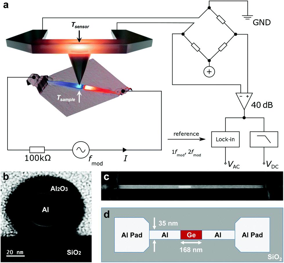 | ||
| Fig. 1 (a) Schematic of the SThM set-up. A slow AC-bias is applied over the device to induce an oscillating sample temperature Tsample which is thermally coupled via the tip to the heated sensor. The signal is de-modulated with a lock-in amplifier at the modulation frequency fmod and 2fmod for measuring the temperature increase due to the Peltier and Joule effect respectively. The simultaneous measurement of the AC- and DC-signal allows to eliminate the thermal resistance between sample and tip and to infer Tsample. (b)–(d) The single crystalline Al–Ge nanowire is electrically connected over Al electrodes and lies on SiO2 substrate. It is naturally integrated in a back-gated FET set-up. (b) shows a dark field scanning transmission electron microscope (DF-STEM) image of the nanowire cross-section, (c) a SEM image and (d) a sketch of the device. | ||
1. Experimental
1.1. Thermal imaging with the SthM
The present SThM setup is operated in a highly shielded lab environment21 in a high vacuum chamber at a pressure of 10−6 mbar. The measured thermal maps have a spatial resolution below 10 nm and mK sensitivity.8 The technique is based on an AFM, where the tip is operated in contact with the sample. The silicon-based temperature sensor is located at the base of the tip and heated to a temperature Tsensor = 273 °C, around which the electrical resistance of the sensor depends linearly on the temperature. When the heated tip is put in contact with the sample, the temperature difference induces a heat flow between the sensor and the sample. A change in sample temperature leads to a change in the heat flux that is detected through a small change in sensor temperature. At the same time, the sample temperature is not expected to be influenced beyond the uncertainty of the method as the thermal resistances within the sample are orders of magnitude lower than the thermal resistance between tip and surface. The nanoscopic contact between tip and sample has typically a resistance of more than 107–108 W K−1 compared to the cantilever leads with a thermal resistance of Rcl ≈ 2 × 10⁵ W K−1. This difference prevents the sensor from equilibrating with the sample temperature.22A major difficulty in the determination of the sample temperature Tsample lies in quantifying the thermal resistance of the tip, the tip–sample contact and the spreading into the substrate. They are all summarized in Rts, which then depends on the surface material, the precise shape of the tip and largely on the size of the touching point that changes with the surface granularity and the topography of the sample. To overcome this problem, the nanowire is operated with an electrical AC-bias of frequency fmod = 1234 Hz that creates a continuously modulated temperature field. Rts is then eliminated in the equations by simultaneous measurement of the time-averaged sensor signal ΔVDC and the de-modulated sensor signal amplitude ΔVAC. An illustration of the set-up is depicted in Fig. 1a. The sample temperature difference to ambient temperature, ΔTsample, for linear devices is then given by8
 | (1) |
An additional feature of the lock-in detection is the possibility to separate the temperature change that is caused by Joule heating and the Peltier effect, respectively. Joule heating, on the one hand, is proportional to the dissipated electrical power and the signal appears at 2fmod. On the other hand, the Peltier effect is directly proportional to the current and produces a thermal signal at 1fmod. Therefore, a detection of SThM-signals at different frequencies allows the separation of Joule and Peltier effects for linear resistors (see below and eqn (4) and (5) for details).
2. Results and analysis
2.1. Temperature maps of self-heated nanowires
Fig. 2 shows the results from a SthM scan at an operating current of 26 μA. (a) is the sample topography from the SThM measurement of the operating nanowire with a spatial resolution of 10 nm. The inferred temperature fields that are induced by Joule heating ΔTJoule and the Peltier effect ΔTPeltier are represented in (d) and (h). Using eqn (1), they are calculated from the DC thermal signal (e), and the AC signals at 2fmod (b) and fmod (f), respectively. The phase signals (c, g) are recorded with the lock-in detector and show the expected behavior for an approximately linear resistor.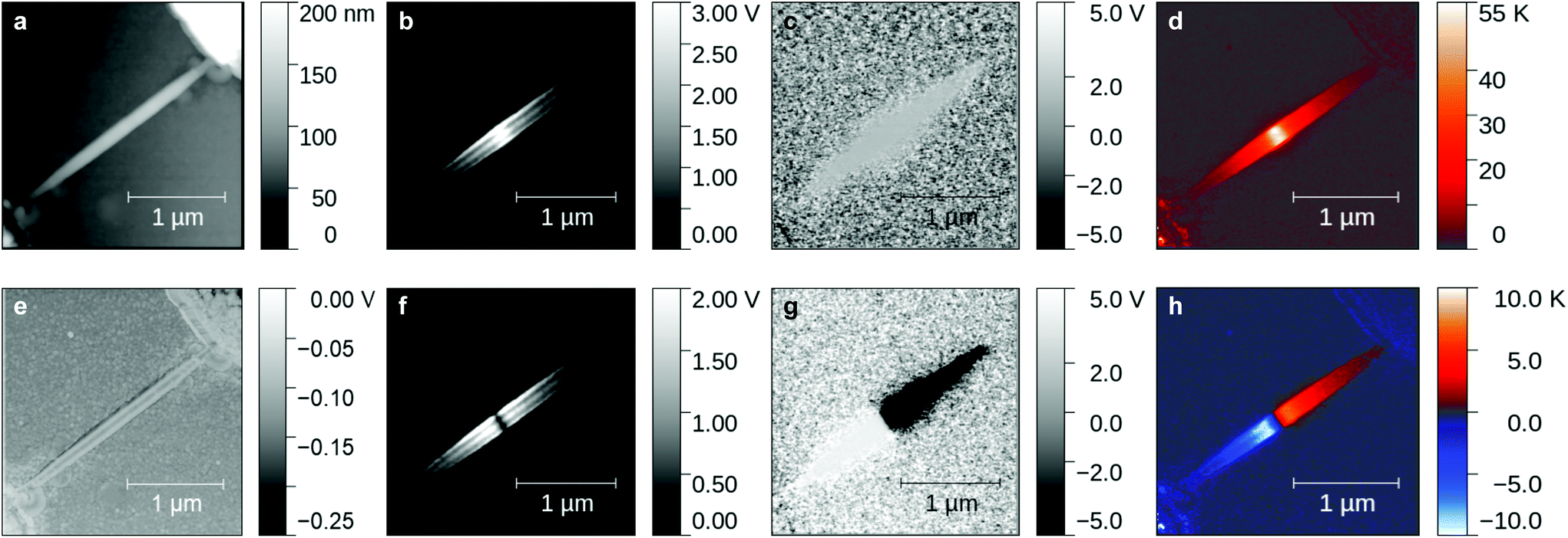 | ||
| Fig. 2 Scanning thermal microscopy data of the wire operating with an AC-current of amplitude I = 26 μA. (a) AFM topography. (b) Thermal signal amplitude taken at 2 fmod in response to Joule heating. (c) Phase of the 2 fmod signal. (d) Joule thermal map calculated using eqn (1) and the scans in (b) and (e). (e) DC-thermal measurement proportional to the thermal resistance of the tip–sample contact. (f) Thermal signal amplitude taken at 1 fmod in response to Peltier heating/cooling. (g) Phase of the 1 fmod AC signal, where ±5 V equals ±90°. (h) Peltier thermal map calculated using eqn (1) and the scans in (e), (f) and (g). | ||
The following analysis concentrates on the line-profiles extracted from the two-dimensional temperature maps of Fig. 2(d) and (h) and according ones for other currents between 13 and 26 μA. The temperature profiles along the long axis of the nanowire are shown in Fig. 3 for both Joule and Peltier signals.
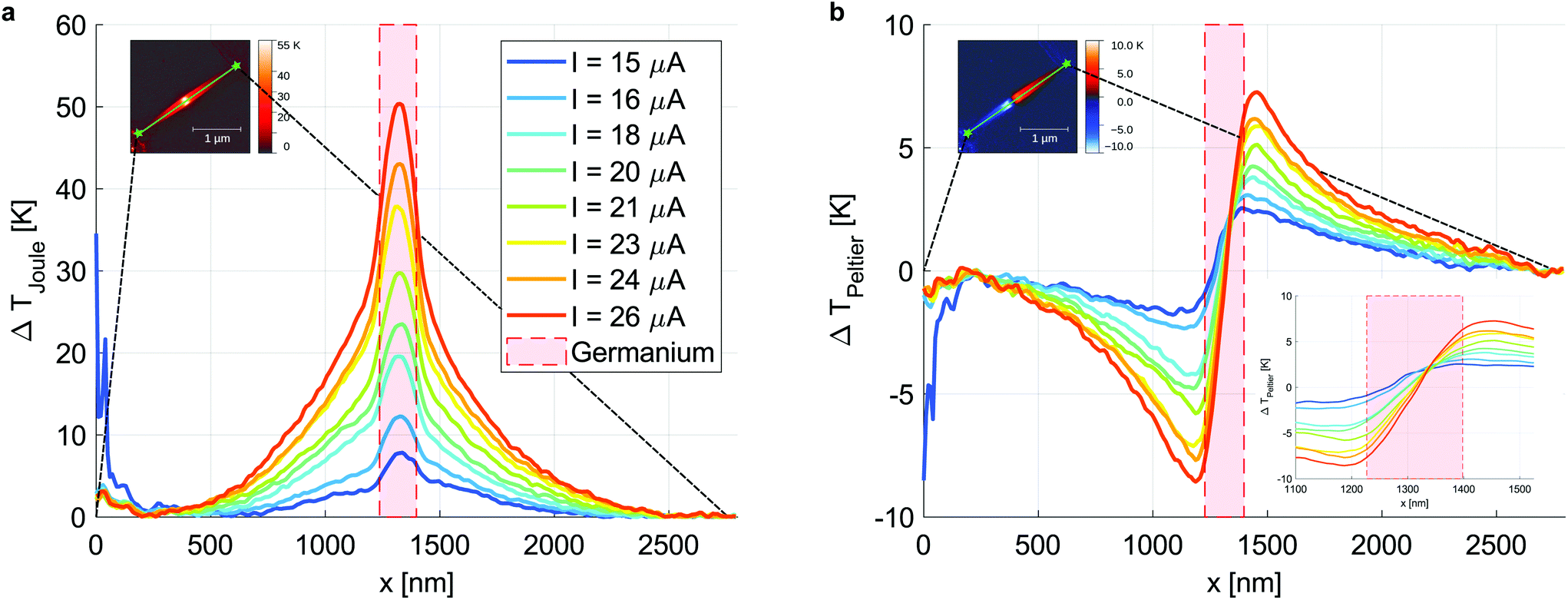 | ||
| Fig. 3 Temperature profiles along the wire with the Ge-segment shaded in red. (a) The temperature change induced by Joule heating ΔTJoule as a function of the position x along the wire, for the operation under increasing voltage biases. (b) The temperature change due to the Peltier effect ΔTPeltier as a function of the position x along the wire operating at different currents I with a zoom on the area of the energy barrier. | ||
2.2. Analysis based on a 1D heat diffusion model
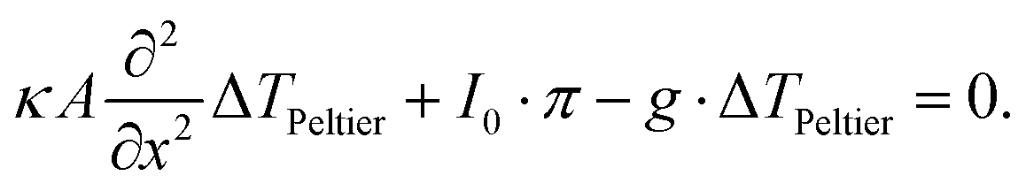
We analyze the data through fitting the experimental temperature profiles to a model based on the one-dimensional heat diffusion equation. It consists of the following contributions: (1) a heat diffusion term, (2) a Joule heating term, proportional to the square of the current I, (3) a Peltier heating term, linearly proportional to the current, (4) a term for heat-loss to the substrate, proportional to the temperature difference between sample and substrate and (5) a term related to the heat capacity CV: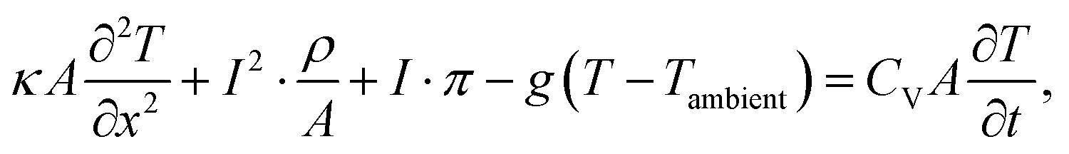 | (2) |
Firstly, the radial temperature distribution can be neglected. This assumption works well for wires with high aspect ratio as in this case. For this composite system we further require that the thermal interface resistance between the core and Al2O3-shell is smaller than that between wire and substrate. While this is a plausible assumption (see below), our study is limited in studying lateral intra-wire effects.
Secondly, the heat spreading into the substrate from a line heat source has no analytical solution. To be able to simplify this into a single thermal conductance term per unit length between a nanowire and the substrate (gΔT) requires, that the thermal interface resistance to the substrate is larger than the spreading resistances within the wire and the substrate. As a first indication, we observe a discontinuity in the horizontal temperature profile between wire and substrate. Fig. 4a shows that the temperature rise along a line section perpendicular to the wire is approximately constant across the nanowire surface and also five to ten times larger than on the substrate. Note, that the wire appears to have a width of 150 nm (instead of the actual 65 nm) due to the well-known convolution effects with the tip shape. In the convolution area and due to the finite diameter of the tip–surface the temperature distribution appears smeared out over some tens of nanometers in this line scan, in contrast to a higher resolution along the nanowire axis.
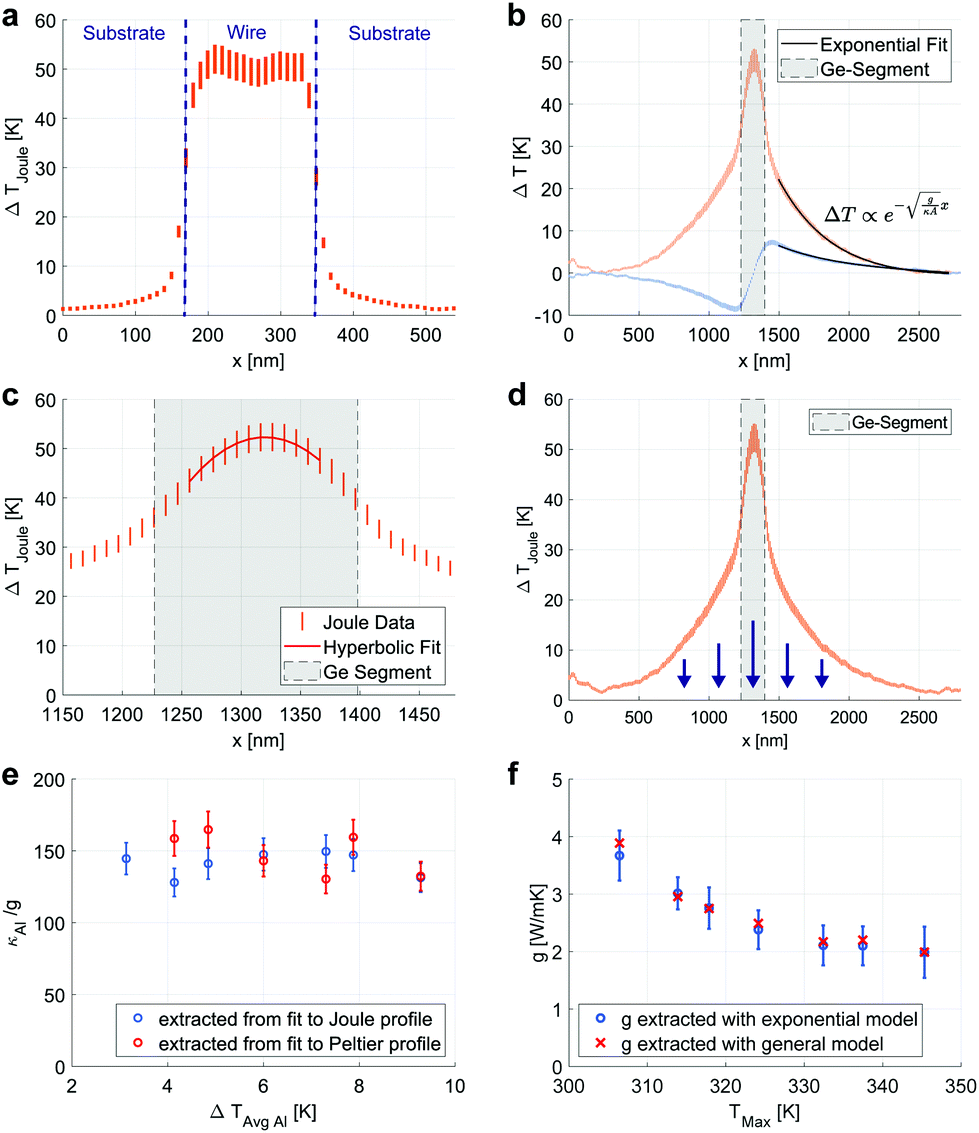 | ||
Fig. 4 Visualization of the parameter extraction. (a) The horizontal profile of the temperature change with respect to RT that caused by Joule heating ΔTJoule. The discontinuity in the temperature profile when going from wire to substrate justifies an analysis in one dimension. (b) The exponential fit in the Al-segment allows to extract the ratio between the thermal conductivity κ and the substrate coupling constant g. The thermal data is marked with the corresponding uncertainty. (c) The thermal conductivity in the Ge-segment is extracted from a hyperbolic fit to the measured temperature change caused by Joule heating in the nanowire. (d) Finally, the substrate coupling constant is calculated via the observation, that all heat dissipated in the wire is lost into the substrate. (e) Shows the values for 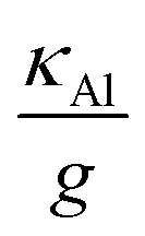 extracted from the exponential fit for the Peltier and Joule profile for different operating currents. (f) Presents the values for the thermal substrate coupling g extracted from the more general model as in (d) (in red) and the values extracted from the exponential fit (in blue). extracted from the exponential fit for the Peltier and Joule profile for different operating currents. (f) Presents the values for the thermal substrate coupling g extracted from the more general model as in (d) (in red) and the values extracted from the exponential fit (in blue). | ||
Thirdly, eqn (2) implies that the transport is essentially diffusive. This is a well established assumption for thermal transport in nanowires of these dimensions with one notable exception where reduced dimensions lead to a ballistic regime.9 However, in this study the observed temperature profiles within the segments are typical for diffusive transport and cannot be explained using ballistic effects. They can be observed only around the interfaces and boundaries, where the spatial resolution of the scan is higher than the carrier scattering length. Near the Ge–Al interfaces, the thermalization lengths of non-equilibrium charge carriers lead to a spatial distribution of the thermoelectric effect.7,15,23 The effective Peltier coefficient is then the integration over the spatial distribution of the local Peltier coefficient
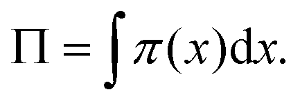 | (3) |
Finally, the AC-modulation period of the driving current is orders of magnitudes shorter than any thermal time constant of the system. Therefore, the scan is taken at steady state and the last term of eqn (2) is negligible.
For a system whose electric response is sufficiently linear, the total temperature distribution is disentangled to T(x,t) = Tambient + ΔTPeltier(x)sin(2πft) + ΔTJoule(x)sin(4πfmodt) for the current I(t) = I0 sin(2πfmodt). The respective thermal profiles are, then, described independently by
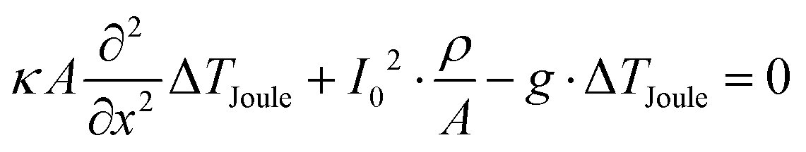 | (4) |
 | (5) |
An initial qualitative observation of the line profiles, shown in Fig. 3, already allows for important conclusions. The Ge and Al sections of the wire exhibit very different characteristics. In the Ge segment, the temperature profile is approximately parabolic, as expected for a diffusive 1D system with uniform Joule dissipation. A heat source term in eqn (2) generally leads to a concave temperature profile. In contrast, the profile in the Al sections is convex, indicative of a situation which is dominated by heat dissipation and loss to the substrate. Here, the approximately exponential decay is expected for a uniform wire without any local Joule dissipation. The Al–Ge interface marks the Joule profiles by a sudden change of slope. When extracting the points of maximum temperature gradient for the Joule signals, their relative distances coincides for all measurements exactly with the length of the Ge segment. Also, after the deflection points there is a transition length of about 40–50 nm in the Al-segments. This area corresponds to the phonon–electron thermalization length that is blurred by a combination of spatial resolution and parallel heat transport in the oxide shell (the figure is in the ESI†). In the Peltier profile we observe the maximum and the minimum of the temperatures some tens of nanometers next to the Al–Ge interface due the spatial distribution of the thermionic effect at the order of the carrier scattering length.
2.3. Analysis of the aluminium leads
We turn first to the sections of the line profiles, in which the core is single crystalline Al. In these sections, the heat diffusion equation has no source terms and therefore reduces to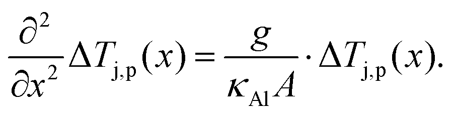 | (6) |
The indices j and p denote Joule and Peltier terms, respectively. As the temperature profile reaches room temperature before reaching the electrodes, the analytic solution to this differential equation is given by
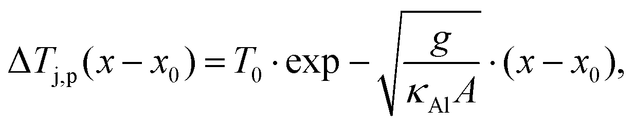 | (7) |
The analysis is pushed further by deriving κAl and g independently. It is observed, that the wire temperature of the Joule profiles decays to room temperature before reaching the electrodes. In other words, the entire heat that is generated over electric power dissipation in the wire (Pdis = I2ρLGe/Acore) is equal to the heat lost to the substrate. By making use of a finite element integral over all the measuring points on the nanowire, the substrate coupling is then the only unknown quantity. The conservation of heat requires
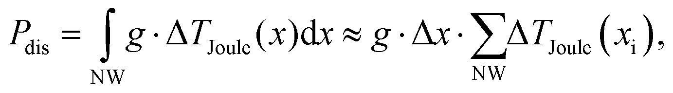 | (8) |
We note that one reaches the same result by considering continuity of heat flux at the Ge–Al interface in addition to the 1D heat diffusion equation. The heat transported into the Al segment is given by ![[Q with combining dot above]](https://www.rsc.org/images/entities/i_char_0051_0307.gif) Al = T(x0)·κAlAwire. The temperature gradient is then calculated from the exponential fit and extrapolated to the Al–Ge interface. Energy conservation implies:
Al = T(x0)·κAlAwire. The temperature gradient is then calculated from the exponential fit and extrapolated to the Al–Ge interface. Energy conservation implies:
| Pdis = 2Al + g·ΔTavgGe·LGe, | (9) |
Next, we turn to the thermal conductivity of the Al segment. Using the extracted values of g and the ratio κ/g, we arrive at a thermal conductivity for the Al segments. To interpret, we need to consider that the value from the fit is an average over the cross section of both the Al core and the Al2O3 shell which are weighed by the respective thermal conductivities and obtain for the core κAl ≈ 150 W (m K)−1. We use the measured cross-sectional areas from the STEM image and the tabulated values for Al2O3. To compare with expected values we apply the Wiedemann Franz law, which results in an electrical resistivity of ρAl ≈ 50 × 10−9 Ω m about twice as high than theoretical predictions for bulk c-Al25,26 which is expected due to increased surface scattering in nanostructures. Indeed, this value is three times lower than previously determined for pure c-Al wires.19 However, in an SThM scan of such an operating c-Al wire a dominant local heat source is identified in the center (see the temperature profiles in the ESI†). This may be expected according to the wire fabrication and indicates a grain boundary. Therefore, the expected values for the electrical conductivity of the c-Al segments without any grain boundary are significantly higher and in good agreement with our experimental value. This result is shows that the influence of grain boundary scattering on the electrical resistivity exceeds the impact of surface scattering in this device. This is typical for polycrystalline nanowires of these dimensions.27 Finally, we would like to mention the importance of taking into account the contribution of an oxide shell to the heat transport in a nanowire.
2.4. Analysis of the germanium section
Next, a value for the thermal conductivity in the Ge-segments is extracted. We note, that the conduction of electrons is limited by the area of the core, whereas the conduction of phonons occurs in both, the Ge and the Al2O3-shell. Eqn (4) becomes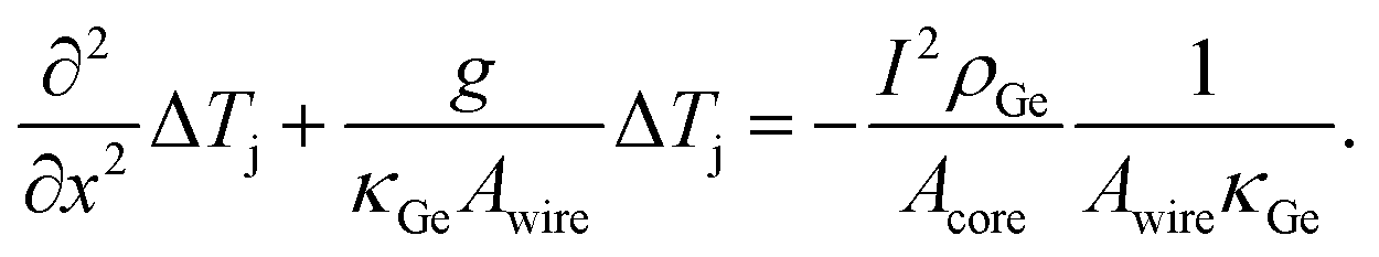 | (10) |
Here, κGe is an average value over core and shell in the Ge segment. This second order differential equation is analytically solved by
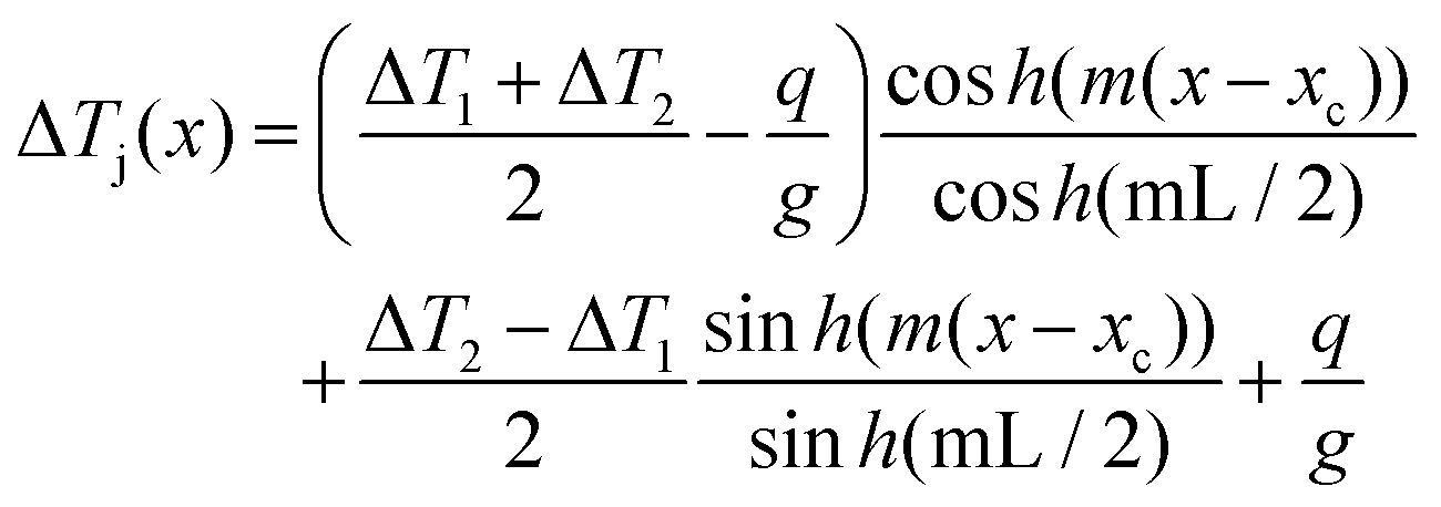 | (11) |
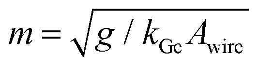 . This function is fitted to the temperature profile in the Ge-segment. In the Casimir result, the mean free path of phonons is limited by the diameter of the nanowire, although in this core–shell system the mean free path may be even smaller than that. The heat diffusion equation, eqn (2), is valid for problems on a larger length scale than the mean free path. Therefore, the points lying closer to the thermal interface than the diameter are excluded for the fitting. Furthermore, to reduce uncertainty of the fit, we fix g from the analysis above and use only κGe and the boundary conditions as a fitting parameter in eqn (11). The fit is shown in Fig. 4c, and the extracted value for the thermal conductivity κGe is 16.9 ± 2.5 W m−1 K−1 at a current of 26 μA.
It is interesting to note, that in this case of relatively small values of m, the temperature profile looks parabolic. For g = 0, supposing that the temperature profile is dominated by Joule heating and heat evacuation towards the electrodes, the solution to eqn (10) would indeed be a parabola. Such a fit seems to match the data well. However, the extracted value is given by κGe = 23.7 ± 3.3 W m−1 K−1 higher by 40% and we conclude that the hyperbolic model should not be simplified.
To interpret the result, we consider that the extracted value for κGe comprises the contributions of both oxide shell and Ge core. The area of the shell is double the area of the core, however, the exact values are measured on the STEM image. Both Al2O3 and Ge crystals have a larger conductivity in bulk, of about 30 and 50 to 60 W m−1 K−1, respectively.28,29 Both values, however, are expected to be significantly reduced, due to the boundary scattering of the phonons at reduced dimensions30 and the measured value is consistent with expectations.
2.5. Extraction of the Peltier coefficient and thermoelectric properties
At this length scale, the distinction between the Peltier effect and thermionic emission becomes blurry. Whereas the Peltier effect exists also in bulk materials, the thermionic effect is understood in a microscopic regime around an energy barrier present at the interface of a heterostructure.31 This region is marked by the thermalization length of the non-equilibrium charge carriers with the lattice. In this analysis, an effective Peltier coefficient is assigned to the thermionic cooling and heating by charge carriers transported over a potential barrier. The local Peltier coefficient is associated with a length scale λ through π(x) = (Π/λ)exp(−(x − x0)/λ). On the scale of λ the non-equilibrium charge carriers equilibrate with the lattice (i.e. the phonon system) after passing the metal–semiconductor interface. Indeed, we observe this distance to be larger than the scattering length of charge carriers for electron–phonon scattering of about 19 to 25 nm.32,33The extraction of the Peltier coefficient is based on the conservation of heat flux at steady state. In the Al wires and near the Al–Ge interfaces, there is either a heat sink or a heat source caused by the Peltier effect GeAl = Π·I or AlGe = −Π·I, respectively, where AlGe > 0 and GeAl < 0, and Π is the Peltier coefficient. An illustration is seen in Fig. 5b. The injected heat from these regions is then equal to the sum of the heat flux towards the Al-electrodes and the heat flux over the Ge-segment to the other heat source/sink. (We can again neglect on the short length scale λ, as discussed above.) By use of Fourier's law the relation is then written as
| = (−κAl∇TAl − κGe∇TGe)·Awire. | (12) |
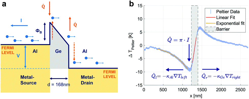 | ||
| Fig. 5 Illustration of the Peltier effect (a) The Fermi energy of electrons in a metal is lower than the average transport energy in a semiconductor. When electrons pass from a metal to a semiconductor they absorb energy from the lattice which creates a local heat sink. On the other side, when electrons pass from the semiconductor to the metal the higher energy electrons thermalize with the lattice which creates a local heat source. (b) The Peltier coefficient is extracted by considering, that the injected heat is equal to the heat flux to the left and the heat flux to the right. The temperature gradients are calculated by help of an exponential fit in the Al-segment and a linear fit in the Ge-barrier. | ||
In order to take into account the above described microscopic extension of the Peltier coefficient we consider the temperature profile beyond the length scale away from the Al–Ge interface. Then we can treat the temperature profiles as solutions to eqn (5) in sections without source terms. The temperature gradient in the Al-segment is the derivative with respect to the position x of the exponential fit to the Peltier profile evaluated at the junction as 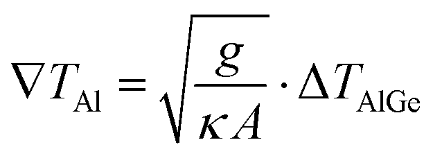 , see eqn (7). By extrapolating the exponential fit we conceptually concentrate the extended heat source in a point at the AlGe interface. The temperature gradient in the Ge-segment is obtained from a linear fit to the data between heat source and heat sink. The linearity of the temperature profile within the Ge section is a result from the strong temperature gradient and the κ/g ratio which justifies neglecting substrate loss g in this region. The effective Peltier coefficient is then calculated as Π = 267 ± 25 mW A−1, resulting in a Seebeck coefficient of S = 790 ± 95 μV K−1 for the temperature at the Al–Ge interface.
It is interesting to relate the effective Peltier coefficient to the Schottky barrier height to test the validity of the derived value. The cooling power by thermionic emission over a barrier is given by the total current times the average energy of the carriers over the barrier
 | (13) |
Hence, the barrier height may be calculated from our measurements. We find φc = 325 ± 45 meV, which is in agreement with previously determined barrier heights from gating experiments of similar devices.20 Independent of metal type and doping concentrations, metal–germanium junctions form Schottky contacts and exhibit very strong Fermi-level pinning close to the valence band.34,35 Finally, the thermoelectric figure of merit is calculated for the scan taken at a current of I = 26 μA to be ZT = 0.020 ± 0.005. This finalizes the thermoelectric characterization of the Al–Ge heterostructure nanowire with a segment length of 168 nm from a single measurement.
Lastly, we have a closer look at the Ge–Al interface regions. We acknowledge that extracting quantitative results is hampered by the oxide shell, which does not comprise an interface. However, important observations can nevertheless be made. The conjecture that the Peltier source term has an exponential spatial distribution has testable consequences. As a result of the distributed source term (eqn (3)), the point of maximum temperature should be shifted with respect to the Al–Ge interface. Using the differential equation with this source term and the material parameters extracted above, we calculate that the maximum temperature should be about 46 nm separated from the interface using an equilibration length of 22 nm. This shift is a good estimation with the position of maximum temperature extracted from the experimental temperature profile of 58 ± 10 nm.
3. Conclusion
This study demonstrates the capability to use thermal imaging by SThM for extracting relevant information on material properties and the dynamics of nanoscale devices and structures. Most notably, we were able to obtain the thermal and thermoelectric properties of a model heterostructure from a single measurement. By quantifying the thermal contact resistance between sample and substrate, its effect can be quantified and, in contrast to other techniques, does no longer hamper the measurements. The values are confirmed by independent measurements, such as the derivation of the substrate coupling with two different models and the comparison of the barrier height investigated thermally with previous electrical transport measurements. It appears, there is currently no other method available to extract this set of information from a sample of this size. For thermoelectric applications, the performance of short segments is interesting, and the results create a link between device design and materials properties.Conflicts of interest
There are no conflicts to declare.Acknowledgements
This project has received funding from the European Union's Horizon 2020 research and innovation programme under Grants 482 No. 766853 (EFINED) and No. 767187 (QuIET). The authors gratefully acknowledge financial support by the Austrian Science Fund (FWF): Project No. P29729-N27. The authors further thank the Center for Micro- and Nanostructures for providing the cleanroom facilities.Continuous support from Anna Fontcuberta i Morral, Ilaria Zardo, Marta De Luca, Kirsten Moselund, Heike Riel and Steffen Reidt is gratefully acknowledged.
References
- E. Pop, Nano Res., 2010, 3, 147–169 CrossRef CAS.
- L. Shi, Nanoscale Microscale Thermophys. Eng., 2012, 16, 79–116 CrossRef CAS.
- L. D. Hicks and M. S. Dresselhaus, Phys. Rev. B: Condens. Matter Mater. Phys., 1993, 47, 16631–16634 CrossRef CAS.
- M. Sistani, M. A. Luong, M. I. den Hertog, E. Robin, M. Spies, B. Fernandez, J. Yao, E. Bertagnolli and A. Lugstein, Nano Lett., 2018, 18, 7692–7697 CrossRef CAS.
- M. Y. Swinkels and I. Zardo, J. Phys. D: Appl. Phys., 2018, 51, 353001 CrossRef.
- X. L. Shi, J. Zou and Z. G. Chen, Chem. Rev., 2020, 120, 7399–7515 CrossRef CAS.
- A. Shakouri, E. Y. Lee, D. Smith, V. Narayanamurti and J. E. Bowers, Microscale Thermophys. Eng., 1998, 2, 37–47 CrossRef CAS.
- F. Menges, P. Mensch, H. Schmid, H. Riel, A. Stemmer and B. Gotsmann, Nat. Commun., 2016, 7, 10874 CrossRef CAS.
- D. Vakulov, S. Gireesan, M. Y. Swinkels, R. Chavez, T. Vogelaar, P. Torres, A. Campo, M. De Luca, M. A. Verheijen, S. Koelling, L. Gagliano, J. E. M. Haverkort, F. X. Alvarez, P. A. Bobbert, I. Zardo and E. P. A. M. Bakkers, Nano Lett., 2020, 20, 2703–2709 CrossRef CAS.
- J. Kim, E. Ou, D. P. Sellan and L. Shi, Rev. Sci. Instrum., 2015, 86, 44901 CrossRef.
- T. Wagner, F. Menges, H. Riel, B. Gotsmann and A. Stemmer, Beilstein J. Nanotechnol., 2018, 9, 129–136 CrossRef CAS.
- E. Nasr Esfahani, F. Ma, S. Wang, Y. Ou, J. Yang and J. Li, Natl. Sci. Rev., 2017, 5, 59–69 CrossRef.
- S. Gomès, A. Assy and P.-O. Chapuis, Phys. Status Solidi A, 2015, 212, 477–494 CrossRef.
- F. Könemann, M. Vollmann, T. Wagner, N. Mohd Ghazali, T. Yamaguchi, A. Stemmer, K. Ishibashi and B. Gotsmann, J. Phys. Chem. C, 2019, 123, 12460–12465 CrossRef.
- F. Könemann, I.-J. Chen, S. Lehmann, C. Thelander and B. Gotsmann, Phys. Rev. Appl., 2020, 13, 54035 CrossRef.
- L. Shi, J. Zhou, P. Kim, A. Bachtold, A. Majumdar and P. L. McEuen, J. Appl. Phys., 2009, 105, 104306 CrossRef.
- M. Sistani, P. Staudinger, J. Greil, M. Holzbauer, H. Detz, E. Bertagnolli and A. Lugstein, Nano Lett., 2017, 17, 4556–4561 CrossRef CAS.
- K. El hajraoui, M. A. Luong, E. Robin, F. Brunbauer, C. Zeiner, A. Lugstein, P. Gentile, J.-L. Rouvière and M. Den Hertog, Nano Lett., 2019, 19, 2897–2904 CrossRef CAS.
- F. M. Brunbauer, E. Bertagnolli, J. Majer and A. Lugstein, Nanotechnology, 2016, 27, 385704 CrossRef.
- S. Kral, C. Zeiner, M. Stöger-Pollach, E. Bertagnolli, M. I. den Hertog, M. Lopez-Haro, E. Robin, K. El Hajraoui and A. Lugstein, Nano Lett., 2015, 15, 4783–4787 CrossRef CAS.
- E. Lörtscher, D. Widmer and B. Gotsmann, Nanoscale, 2013, 5, 10542–10549 RSC.
- F. Menges, H. Riel, A. Stemmer and B. Gotsmann, Rev. Sci. Instrum., 2016, 87, 74902 CrossRef.
- R. Lake and S. Datta, Phys. Rev. B: Condens. Matter Mater. Phys., 1992, 46, 4757–4763 CrossRef.
- E. T. Swartz and R. O. Pohl, Rev. Mod. Phys., 1989, 61, 605–668 CrossRef.
- D. Gall, J. Appl. Phys., 2016, 119, 85101 CrossRef.
- A. Jain and A. J. H. McGaughey, Phys. Rev. B, 2016, 93, 81206 CrossRef.
- C. Durkan and M. E. Welland, Phys. Rev. B: Condens. Matter Mater. Phys., 2000, 61, 14215–14218 CrossRef CAS.
- A. M. Hofmeister, Phys. Chem. Miner., 2014, 41, 361–371 CrossRef CAS.
- C. J. Glassbrenner and G. A. Slack, Phys. Rev., 1964, 134, A1058–A1069 CrossRef.
- N. Mingo, L. Yang, D. Li and A. Majumdar, Nano Lett., 2003, 3, 1713–1716 CrossRef CAS.
- D. M. Rowe, Thermoelectrics handbook : macro to nano, Taylor & Francis, Boca Raton, 2006 Search PubMed.
- W. M. Haynes, CRC handbook of chemistry and physics, CRC press, 2014 Search PubMed.
- H. Kanter, Phys. Rev. B: Solid State, 1970, 1, 522–536 CrossRef.
- A. Thanailakis and D. C. Northrop, Solid-State Electron., 1973, 16, 1383–1389 CrossRef CAS.
- A. Dimoulas, P. Tsipas, A. Sotiropoulos and E. K. Evangelou, Appl. Phys. Lett., 2006, 89, 252110 CrossRef.
Footnote |
| † Electronic supplementary information (ESI) available. See DOI: 10.1039/D0NR05504B |
| This journal is © The Royal Society of Chemistry 2020 |