
 Open Access Article
 This Open Access Article is licensed under a
 Creative Commons Attribution 3.0 Unported Licence
Recent progress in hybrid perovskite solar cells through scanning tunneling microscopy and spectroscopy
Sanjay
Sahare
 ab,
Prachi
Ghoderao
c,
Sadaf Bashir
Khan
ab,
Yue
Chan
a and
Shern-Long
Lee
*a
ab,
Prachi
Ghoderao
c,
Sadaf Bashir
Khan
ab,
Yue
Chan
a and
Shern-Long
Lee
*a
aInstitute for Advanced Study, Shenzhen University, Shenzhen, Guangdong, 518060 China. E-mail: sllee@szu.edu.cn
bLaboratory of Optoelectronic Devices and Systems of Ministry of Education and Guangdong Province, College of Optoelectronics Engineering, Shenzhen University, Shenzhen, Guangdong, 518060 China
cDepartment of Applied Physics, Defence Institute of Advanced Technology, Pune, 411025 India
First published on 7th July 2020
Abstract
Currently, sustainable renewable energy sources are urgently required to fulfill the cumulative energy needs of the world's 7.8 billion population, since the conventional coal and fossil fuels will be exhausted soon. Photovoltaic devices are a direct and efficient means to produce a huge amount of energy to meet these energy targets. In particular, hybrid-perovskite-based photovoltaic devices merit special attention not only due to their exceptional efficiency for generating appreciable energy but also their tunable band gaps and the ease of device fabrication. However, the commercialization of such devices suffers from the instability of the compositional materials. The cause of instability is the perovskite's structure and its morphology at the sub-molecular level; thereby revealing and eliminating these instabilities are a striking challenge. To address this issue, scanning tunneling microscopy/spectroscopy (STM/STS) presents a comprehensive method to allow the visualization of the morphology and electronic structure of materials at atomic-level resolution. Here, we review the recent developments of perovskite-based solar cells (PSCs), the STM/STS analysis of photoactive halide/hybrid and oxide materials, and the real-time STM/STS investigation of electronic structures with defects and traps that are believed to mainly affect device performances. The detailed STM/STS analysis can facilitate a better understanding of the properties of materials at the nanoscale. This informative study may hold great promise to advance the development of stable PSCs under atmospheric conditions.
 Sanjay Sahare | Sanjay Sahare is a Post-Doctoral fellow at Institute for Advanced Study, Shenzhen University, China. He received his Master's and Ph.D. from RTMNU, Nagpur, and Defence Institute of Advanced Technology, Pune, India, respectively. His research interests include Scanning probe microscopy, Micro fabrication techniques and Hybrid solar cells. |
 Shern-Long Lee | Shern-Long Lee received his PhD in chemistry in 2009 from National Taiwan University. During his doctoral work, he studied supramolecular self-assembly via scanning probe microscopy (advisor: Prof. Chun-hsien Chen). In 2009–2012, he worked as a postdoc in the same group, after which he did his second postdoc (Marie Curie, 2012–2015) in Prof Steven De Feyter's group at KU Leuven in Belgium. He is now a researcher of IAS at Shenzhen University (China) where his research interests include materials and analytical chemistry. |
1. Introduction
Energy consumption is becoming an international issue faced by everyone throughout the world. Sustainable and renewable energy resources are playing a crucial role in fulfilling the cumulative energy needs of the world's population. In this aspect, photovoltaic (PV) devices are a straightforward and highly efficient means to produce an enormous amount of energy. In particular, perovskite solar cells (PSCs) belong to an emerging thin-film PV cell class that consists of perovskite structured compounds and exhibits high energy conversion efficiency. Therefore, PSCs have become a global research hotspot in the PV arena.1–4 The energy conversion efficiency of PSCs has shown the steepest growth, which has crossed 24.5% thus far.5 Besides, it has been predicted that perovskites play a critical role in next-generation lasers, sensors, electric vehicle batteries, etc.6–8 However, the lack of a comprehensive understanding of the morphology and photo-physics of perovskite-based materials along with their stability issues largely hamper their progression.9–11 The surface morphology and band energy levels directly influence the potential difference of a device, and thus the spatial transportation of charge carriers over time.12,13 Therefore, exploring the thin-film morphology and the electronic transport in perovskite materials is of key interest in this emergent field. The performance of perovskite-based optoelectronic devices is influenced by various electrical parameters, such as current–voltage (I–V) hysteresis, trap states, charge carrier recombination, and ion migration, which are commonly defined by the morphologies of the film.14–18 Even a minute variation in sample preparation can lead to huge discrepancies in the resulting thin films.19–21 Consequently, changes in the aforementioned electrical parameters could determine the PV efficiency. Therefore, a thorough study of thin films at the nanoscale level is essential to reveal such structural problems to fabricate more efficient PV devices.22,23Generally, X-ray diffraction (XRD), X-ray photoelectron spectroscopy (XPS), UV-Vis spectroscopy, photoluminescence, and I–V measurements are common techniques for the detailed analysis of perovskite thin films. Unfortunately, these traditional techniques cannot provide real spatial resolutions. In this regard, scanning probe microscopy (SPM) has been utilized to obtain detailed information down to the atomic-level resolution of organic and inorganic PV materials.24–28 Numerous SPM techniques including scanning tunneling microscopy (STM), non-contact atomic force microscopy (AFM), Kelvin probe force microscopy (KPFM), and conductive-AFM (c-AFM) have been proposed to unveil the heterogeneities in perovskite thin films.29–34 Among AFM techniques, KPFM and c-AFM have been widely used to probe the photo-voltages and photo-currents of perovskite grains and their boundaries. In particular, KPFM, a non-contact AFM technique has contributed significantly to the identification of the local work function of samples by real-time visualization.30 This unique technique can provide surface information, including the composition and electronic states. Such a technique has been used to investigate the charge-separation locations, trap states, and different phases in perovskite materials by tracing the potential fluctuations.35–39 Similarly, STM can provide information about the structure, electronic properties, and electronic states (e.g., concerning the Fermi level of the electrode, Fig. 1) with a high spatial resolution (0.1 nm).40,41 In contrast to c-AFM, the tunneling current between the STM tip and the sample surface is measured by moving the conductive tip without physical contact across the sample surface and thus no damage occurs to samples. According to the quantum mechanical phenomenon, the tunneling current between the STM tip and sample (∼1.0 nm) can occur once a voltage bias is applied.42 The tunneling current exponentially increases as the tip–sample distance reduces. This mechanism allows us to obtain high-resolution spatial images of surfaces of materials in real space (lateral resolution below 10 pm and a vertical resolution <1 pm). These defects at the atomic scale can strongly influence the behavior and performance of the photo-absorber layers and hence the efficiency of a device. One can see an overview of the STM measurement technique and its measurement ability (the type of sample analysis) at the atomic level in Fig. 1. This schematic depicts the formation of the tunneling junction between the sample and metallic tip, where electrons get tunneled from the sample to the tip or vice versa against the applied bias.43 Once the perfect topography is obtained at this particular location, the tunneling current can be measured. Furthermore, the measured current will be utilized to estimate the bandgap and density of states (DOS) of the materials. Also, the band alignment can be estimated for the appraisal of rapid charge transfer and its separation upon illumination at the heterojunction, which produces a photocurrent in the external circuit.44
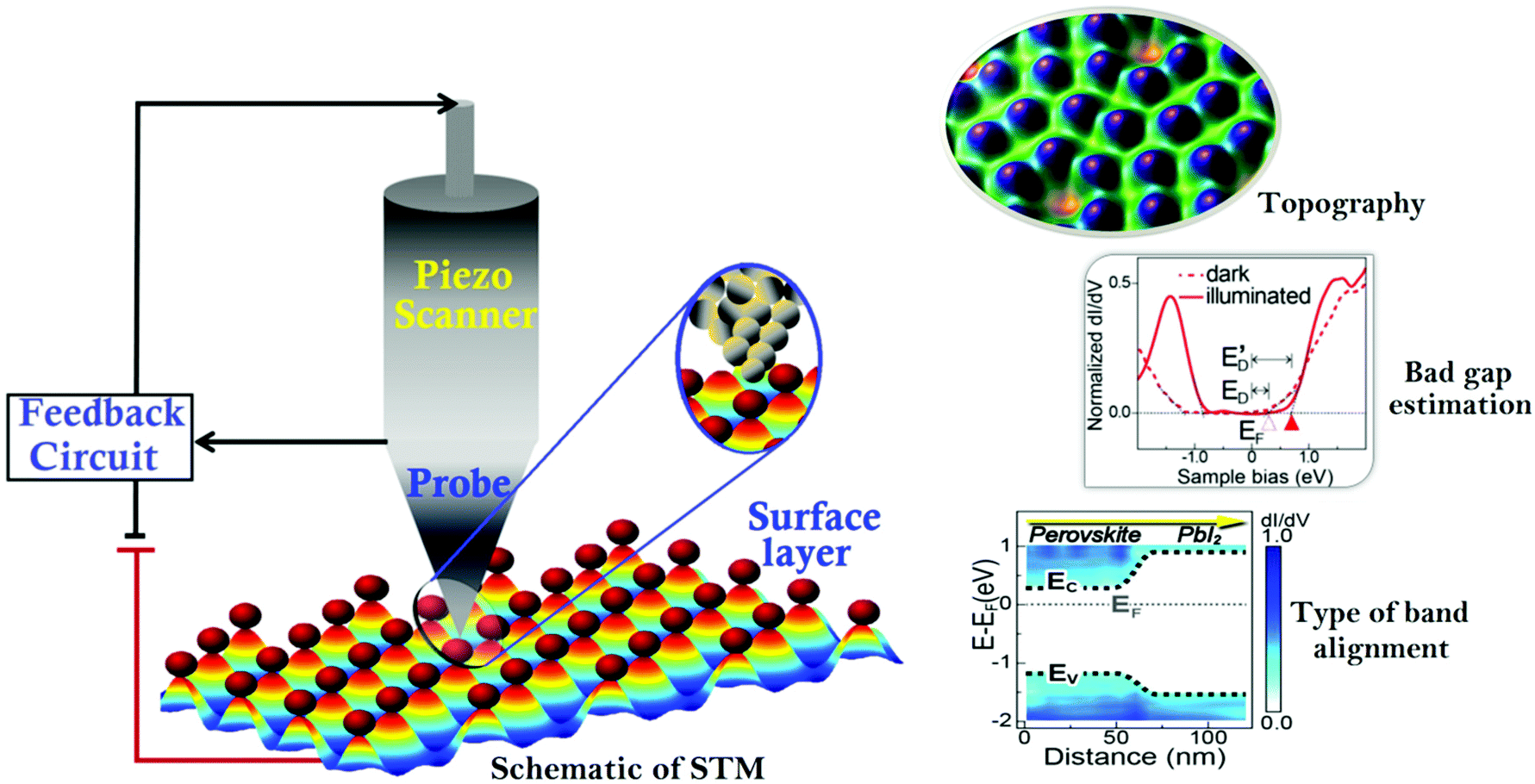 | ||
| Fig. 1 An overview of the STM measurement technique and types of analyses (band gap estimation and alignment. Reproduced with permission from ref. 48). | ||
To date, huge progress has been achieved in the performance enhancement of PSCs. Despite its significance, the analysis of PSCs via STM at the atomic scale has been rarely discussed. Abundantly existing literature reports have mentioned genuine hurdles regarding the issue of sample preparation; however the protocols to be followed for performing accurate STM measurements for PSCs remain elusive.45–47 So far, it remains a challenge to establish the specific sample-preparation methods for perovskite materials. Due to this limiting factor, the correlation of physical and chemical properties at the atomic level has not been thoroughly inspected in STM/STS analysis.
In this contribution, we present an overview of STM measurement techniques, where using a specific strategy, real-time electronic structures of the perovskite materials have been studied. Here, we discuss the STM analysis of two types of perovskite materials, namely, halide and oxide perovskite materials in the view of solar cell applications. In addition, we will discuss the sample preparation techniques/methods for STM investigations, which are crucial to obtain precise information regarding the interfacial properties of perovskite heterostructures. We anticipate that this review can offer substantial useful information, i.e. pros and cons of sample preparation that can extend toward atomic-level studies. These factors could be essential for researchers to assemble optimal materials in PV devices to enhance the stability and overall performance of hybrid PSCs.
2. Perovskite synthesis and sample preparation techniques
A specific sample-preparation procedure for better STM investigation is the most critical aspect to make a conclusive affirmation about the fundamental properties of perovskite materials. Technically, an immaculate and atomically flat surface is essential to obtain flawless STM images (morphology and structures), which are normally impossible to be obtained with perovskite materials.49 In this process, the substrate also plays an important role, since the morphology and topography of the film always depend upon the properties of the underlying substrate.50,51 Similarly, ITO/FTO coated glass, Au, Cr, and HOPG are commonly used as conducting substrates for electrical contacts in the process of STM sample preparation.52–54 Synthesis of a perovskite material is the first step towards the sample preparation for STM analysis. Researchers have used different methods to synthesize or prepare perovskite photon absorbing layers on different substrates. These synthesized samples can be used as it is, or sometimes we need to follow surface processing treatments (e.g. cutting and polishing) on it to make a more ideal sample for obtaining high-resolution STM images.47 The schematics of a few perovskite synthesis methods (e.g. solution process, vacuum, and chemical vapor deposition) and sample preparation techniques e.g. the cleaving method are shown in Fig. 2 and 3, respectively. The details of these techniques are given as follows.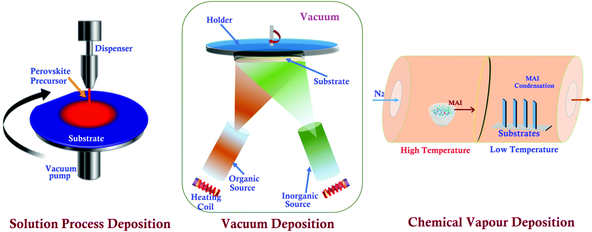 | ||
| Fig. 2 Perovskite synthesis/deposition methods. | ||
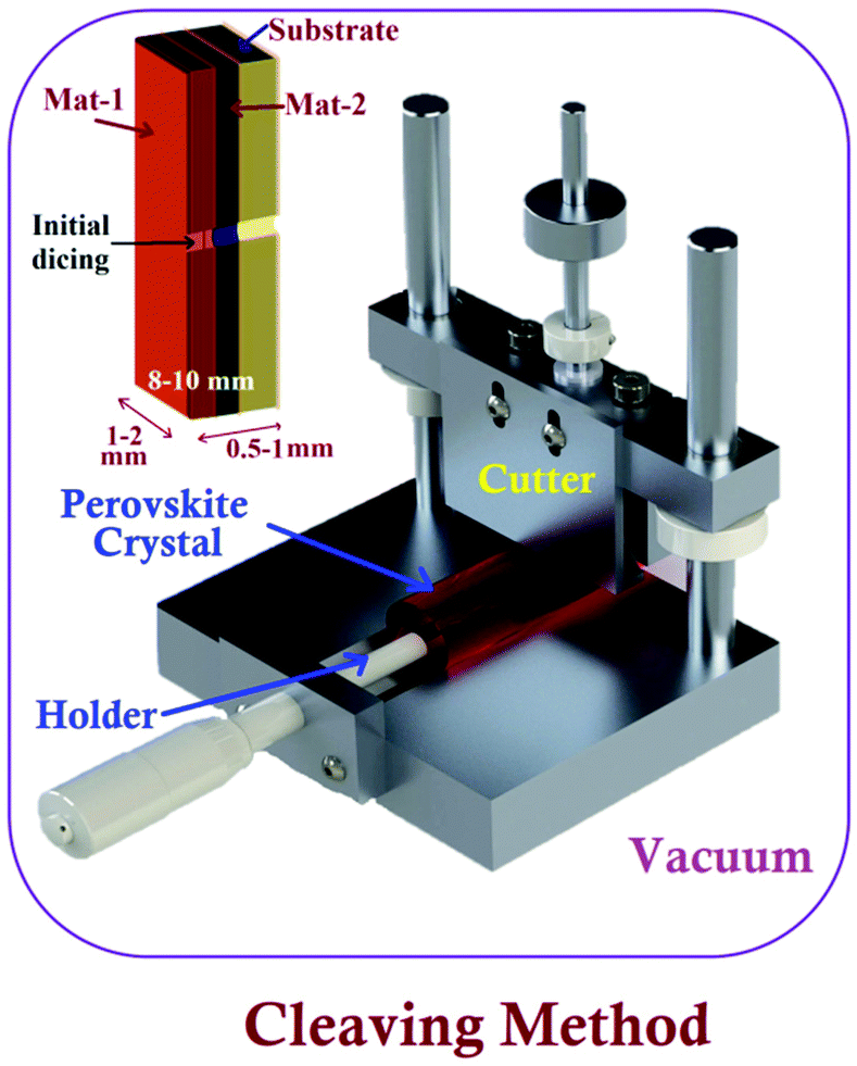 | ||
| Fig. 3 Experimental set-up of the cleaving method to prepare XSTM/S samples. Inset figure shows basic sample preparation using initial dicing. | ||
2.1. Perovskite synthesis methods
![[thin space (1/6-em)]](https://www.rsc.org/images/entities/char_2009.gif) :3 ratio of PbCl2/CH3NH3I in DMF) was spin-coated onto an As-doped Si (100) substrate at 1500 rpm, followed by annealing (90 °C for 2 h) under a nitrogen atmosphere.59 The deposited perovskite sample can be cleaved with the desired facet for carrying out an appropriate STM study.
:3 for CH3NH3I and PbI2. The film was ∼10.8 atomic layer thick and smoother for further STM measurements. Likewise, an MAPbBr3 thin film was grown on a Au (111) single crystal surface by dual-source vacuum co-evaporation of the MABr and PbBr2 species for 10 min at evaporation temperatures of 361 and 498 K, respectively.63 On the other hand, in such a sequential co-evaporation technique, since the MAI layer was deposited over a metal halide layer, the MAI diffusion depth was limited, leaving the bottom metal halide layer unreacted.64 The stoichiometry of precursors (e.g., MAI and PbI2) has been controlled using a well-established and compatible technique for temperature-sensitive devices having high throughput and reliability in the electronic industries. The oxide perovskite (LSMO) has been deposited using pulse-laser deposition (PLD) on a Si substrate by Joshi et al.65 The growth conditions for the deposited films were optimized (KrF excimer laser, 248 nm wavelength, and 30 ns pulse width) and images were taken from the top surface of the deposited film. S. Wang et al. have examined the local electronic structure of oxide (perovskite) thin films deposited with a pulsed laser deposition system in conjunction with low-temperature STM measurements. In addition, they have modified the vacuum-deposition and developed a hybrid deposition technique by facilitating advanced tools and accessories to obtain an extremely smooth surface with high crystallinity, and the maximum surface coverage with a uniform chemical composition throughout the whole film.60
:3 ratio of PbCl2/CH3NH3I in DMF) was spin-coated onto an As-doped Si (100) substrate at 1500 rpm, followed by annealing (90 °C for 2 h) under a nitrogen atmosphere.59 The deposited perovskite sample can be cleaved with the desired facet for carrying out an appropriate STM study.
:3 for CH3NH3I and PbI2. The film was ∼10.8 atomic layer thick and smoother for further STM measurements. Likewise, an MAPbBr3 thin film was grown on a Au (111) single crystal surface by dual-source vacuum co-evaporation of the MABr and PbBr2 species for 10 min at evaporation temperatures of 361 and 498 K, respectively.63 On the other hand, in such a sequential co-evaporation technique, since the MAI layer was deposited over a metal halide layer, the MAI diffusion depth was limited, leaving the bottom metal halide layer unreacted.64 The stoichiometry of precursors (e.g., MAI and PbI2) has been controlled using a well-established and compatible technique for temperature-sensitive devices having high throughput and reliability in the electronic industries. The oxide perovskite (LSMO) has been deposited using pulse-laser deposition (PLD) on a Si substrate by Joshi et al.65 The growth conditions for the deposited films were optimized (KrF excimer laser, 248 nm wavelength, and 30 ns pulse width) and images were taken from the top surface of the deposited film. S. Wang et al. have examined the local electronic structure of oxide (perovskite) thin films deposited with a pulsed laser deposition system in conjunction with low-temperature STM measurements. In addition, they have modified the vacuum-deposition and developed a hybrid deposition technique by facilitating advanced tools and accessories to obtain an extremely smooth surface with high crystallinity, and the maximum surface coverage with a uniform chemical composition throughout the whole film.60
2.2. Sample preparation techniques
The cross-sectional STM and STS (XSTM/S) are advanced techniques of STM, which can help achieve band mapping at heterojunction interfaces.80 This can be performed by creating a dirt-free surface of the cross-section by fracturing the material.76,81 For getting a sharp interface, the sample should be cut into long strips with the high precision dicing saw, where in situ fracture can be induced by applying steady force in a UHV environment.82 A schematic of the prepared strip is shown in the inset of Fig. 3. The success rate of XSTM/S sample preparation with an initial dicing process is about 70 to 80%. For performing such experiments, special attention should be paid to the following factors such as obtaining a flat and defect-free cross-sectional surface to pin the Fermi level at the surface and, also, maintaining a specific height of the metallic tip consistently over the precise location of interest on the cross-sectional surface.83 Murali et al. have demonstrated their sample preparation methods under ultra-high vacuum (5 × 10⁻¹⁰ mbar) with a sharp blade, fixed on another sample holder, supported with a linear-rotary-motion feedthrough.84 The facets of the single crystal perovskite were sharply cut down into parallel planes with a size of 2–3 mm, followed by in situ electron bombardment to achieve an atomic-scale surface reconstruction for STM imaging and measurements. In addition, hybrid perovskites were synthesized in the form of thin films using different methods. Therefore, these samples sometimes would not be suitable for interfacial/cross-sectional study due to their sizes, the underlying substrate, and other compatibility issues. In these circumstances, the samples need to be cleaved or fractured precisely in such a way that the desired facet can be viewed. Such an established system can be a potential platform for STM sample preparation and conducting studies to tune the surface properties at the atomic scale.
3. Perovskite analysis by STM and STS
STM and STS are the surface analytical techniques, capable of probing the DOS with a high spatial and energetic resolution.85,86 STM has contributed significantly to understand the sub-processes included in the fundamental phenomenon of PV. Notably, in organic solar cells, the exciton binding energy, electrostatic potential distribution, and charge transfer mechanism play an important role in intermolecular interactions of hybrid semiconductors.87,88 However, STM is a powerful technique to visualize the self-assembled monolayers at the atomic scale, from which one can correlate the performance of organic solar cells.89–91 When probing, a mechanically cut or chemically etched sharp tip is brought close to the sample surface (∼2–10 Å). A platinum–iridium (Pt–Ir) tip is commonly used to probe the sample due to its strength and stability.92,93 Electrons can tunnel into the empty states or accept it from the filled states depending on the applied bias (polarity) between the tip and the sample, deposited on the conductive substrate. This tunneling phenomenon occurs due to the energetic alignment between the work function of the tip and the sample energy levels with respect to the magnitude of the STM applied bias. Therefore, the level and location of conduction as well as the valence band (CB and VB) can be easily determined through the differential conductance (dI/dV) spectrum (STS). The images obtained by STS can illustrate energy level mapping over the scanned area, particularly to analyze local electronic properties along with the visualization of a few hundred atoms accurately.44 In the view of significant challenges in obtaining local properties, here we will discuss the microscopic and spectroscopic analyses in halide/hybrid and oxide perovskites for PV applications.3.1. Halide perovskites
As we discussed earlier, halide-perovskite-based solar cells are much more rapidly growing PVs. However, their commercialization is not yet possible because of their instability and toxicity. Various groups have analyzed thin-films and devices through different characterization techniques, and suggested fruitful solutions toward high-performance PVs, including the synthesis of defect-free perovskites, diverse deposition techniques, use of different transport layers and protective coatings, etc.94–99 The structural, morphological, and electro-optical characterization analyses provide an easy means to understand the behavior of perovskites, although as stated previously, atomic analysis is not yet fully explored due to sample constraints. Miyasaka et al. have used halide perovskites, e.g. MAPbI3, for the first time in dye-sensitized solar cells (DSSCs) as sensitizers in 2009.100 However, the sample preparation issues exist due to small crystal size and degradation, hence halide perovskite took a long duration to observe its atomic structures through STM. Until 2015, Ohmann et al. observed the atomic structure of MAPbBr3 with high spatial resolution by STM.45 These measurements were possible because of the bigger size single crystal that was easy to cleave and hence we can obtain a flat surface under ultra-high vacuum (UHV). One of the advantages of working under the UHV conditions is that one can obtain a superior control over the surface, which further makes it easier to study the single-molecule, sub-monolayer structures, and isolated clusters.101,102 | ||
| Fig. 4 (a) Atomic resolution of an MAPbBr3 resolved STM topography image of the perovskite surface. Height profile along the dashed line shown in the inset of (a); (b) simulated STM image of the (010) plane of the orthorhombic crystal with surface reconstruction. Br and MA ions are overlaid. The orientation of MA leads to different domains; (c) STM topographic image of another domain apart from that shown in (a). The arrows and dashed lines indicate the direction of the height profiles. (d) Corresponding calculated image of (c); (e) comparison of height profiles along perpendicular directions for two different observed domains and their corresponding models. Arrows indicate the rotational and positional changes of MA molecules and Br ions, respectively, between the ferroelectric and anti-ferroelectric domains. (a–e) Reproduced with permission from ref. 45. | ||
With regard to the electronic properties, DOS has been studied using STS, in which the tip gets stabilized at a fixed location above the surface with varying voltages. A typical STS spectrum (a derivative of I–V) and calculated DOS are shown in Fig. 5a and b. An interesting aspect arises, when only for a negative bias, it depicts a significant differential conductance (dI/dV), and reveals the occupied states of the surface. On the other hand, it does not show an appreciable tunneling current indicating unoccupied states against the applied positive bias. This result is surprisingly consistent with STM images, and it is difficult to obtain topographic images upon an applied positive bias (not shown here). The partial DOS has been calculated and it strongly supports this observation (Fig. 5b). The DOS clearly illustrates the characteristics of ferroelectric and anti-ferroelectric domains leading to different electronic structures. Similarly, the dissimilar electronic phases tend to favor domain orientations in the normal direction of the thin-film surface. These orientations can alter the electronic properties of the materials.
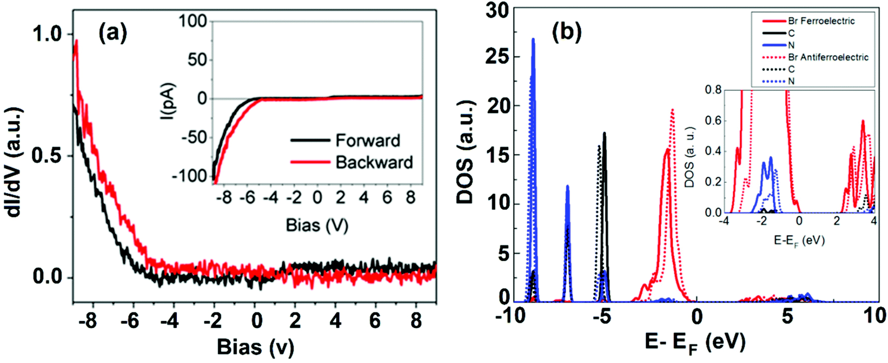 | ||
| Fig. 5 (a) Scanning tunneling spectroscopy (dI/dV) on the perovskite surface. Inset: Simultaneously acquired I–V curve. (b) Comparison of density of states calculations on two different domains: ferroelectric (solid line) and anti-ferroelectric (dotted line). Inset shows a zoom-in of the energy region close to the Fermi level. (a,b) Reproduced with permission from ref. 45. | ||
The origin of the MAPbI3 perovskite surface and the phase transition between two surfaces have been revealed by She and co-workers.46 The zigzag and the dimer phase structures were found at MA–I-terminated (001) surfaces by STM. The zigzag row follows the original structure of the (001) planes in the bulk, and later on it exhibits iodine dimer rows with a shortened I–I distance for each dimer. The authors explained such iodine dimerization subsequently by net charge distribution and surface polarization. Fig. 6a shows an atomically smooth large-scale STM image of MAPbI3 films with step edges on the Au (111) substrate. High-resolution STM images showed two types of surface structures, namely the zigzag phase (Fig. 6b) and the dimer phase (Fig. 6c). The structures consist of a quasi-square unit cell with two bright protrusions per unit cell. In the zigzag phase, the bright protrusion (green rectangles) slightly deviated from the center, and redirected toward both the corners of the unit cell resulting in zigzag rows (Fig. 6b). The dimer phase formation was due to the bright protrusions shifting toward a corner of the unit cell (Fig. 6c). In addition, both phases were observed in the same region, with a height difference of less than 10 pm (Fig. 6d). The obtained orthorhombic perovskite structure with a periodic stacking of two PbI6 octahedra along the c-axis (001) is terminated by MA–I or Pb–I. The prediction of MA–I or Pb–I termination is made based on the induction of the tunneling current during STM scanning, where zigzag and dimer phases can convert into each other (Fig. 6f-i, ii, iii). In the process of phase conversion, in both cases, the band gaps of around 1.7 eV remain intact for the structures. The band gaps were measured at different locations of zigzag and dimer structures. MA–I or Pb–I termination has also been verified through DFT calculations. The simulated STM image is quite similar to that of the experimental result (Fig. 6b), in which the iodine anions denote bright dots and the MA cations are invisible in the figure confirming the MA–I-terminated surface of MAPbI3 films. DFT calculations supported the formation of I dimers, ascribed to the electrostatic interactions with the re-oriented MA cations. Similarly, MAPbBr3 surface reconstruction through Rashba splitting has been discussed.103 Special attention has been paid to the surface relaxation and the changes in their electronic properties. In the computational studies, the surface reconstruction of the (001) oriented facets of MAPbBr3 occurs in its orthorhombic phase, where the collective orientations of MA cations generate the dimer and zigzag phases corroborating the structure provided by the previous STM experiments.46,63 Such analysis reveals the crucial role of MA cations as rotatable dipoles in the surface reconstruction and phase transition so that researchers can benefit from understanding the microscopic behavior of halide perovskites.
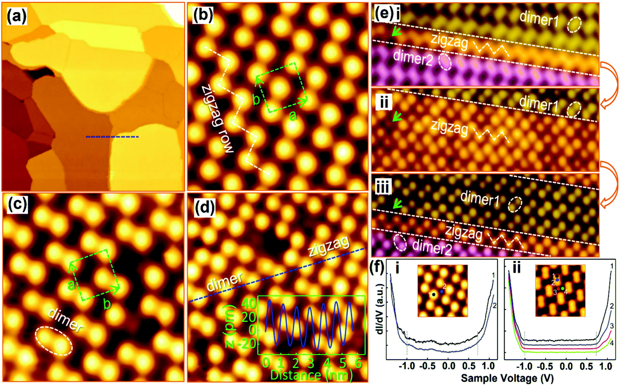 | ||
| Fig. 6 STM images of MAPb3 films deposited on Au(111). (a) Large-scale image (300 × 300 nm2) with atomically flat terraces; (b and c) high-resolution images of the zigzag and dimer structures (4.3 × 4.3 nm2). The unit cells are denoted by dashed rectangles. A zigzag row is indicated by the dashed line in (b), and an iodine dimer is denoted by a dashed ellipse in (c); (d) STM image of the two phases coexisting at the same region (5.6 × 5.6 nm2); (e-i, ii, iii) sequential STM images acquired at the same region showing the reversible transition between the dimer and zigzag structures (4.2 × 12.8 nm2); and (f-i, ii) dI/dV spectra acquired from different sites of the two surface structures: (i) zigzag and (ii) dimer. (a–f) Reproduced with permission from ref. 46. | ||
Furthermore, Stecker et al. have demonstrated the ion transport mechanisms at the surface, in the crystal direction, by both the theoretical and experimental approaches at the atomic level.63 They have further explored and confirmed the occurrence of vacancy-assisted transportation of the separate ions and vacancy defect clusters at the MAPbBr3 surface. In particular, the identification of intrinsic vacancies/defects on the surface of MAPbBr3 is shown in Fig. 7. The pristine surface ions of MAPbBr3 are also shown in Fig. 7a, where a bright protrusion depicts a Br− ion. The pairing took place due to the electrostatic interactions between two adjacent Br anions with positive nitrogen atoms (blue atoms, Fig. 7a), in which defect occurs. One can observe different types of intrinsic defects at the atomic scale from the STM image. An unpaired Br anion defect occurs because of the pair orientation mismatch in the same row (Fig. 7b). If some nearby vacancies occur, the adjacent unpaired Br defects can be observed (Fig. 7c). These vacancies are responsible for forming another type of defect, observed as dark depressions in the STM image (Fig. 7d). Subsequently, this leads to the formation of double and triple vacancies/defects (Fig. 7e and f). Theoretical calculations show that for a single MABr vacancy, there is a 90° rotation of the MA cation close to the defect with the nitrogen end of the dipole near the unpaired Br− (Fig. 7g, dashed black circle).
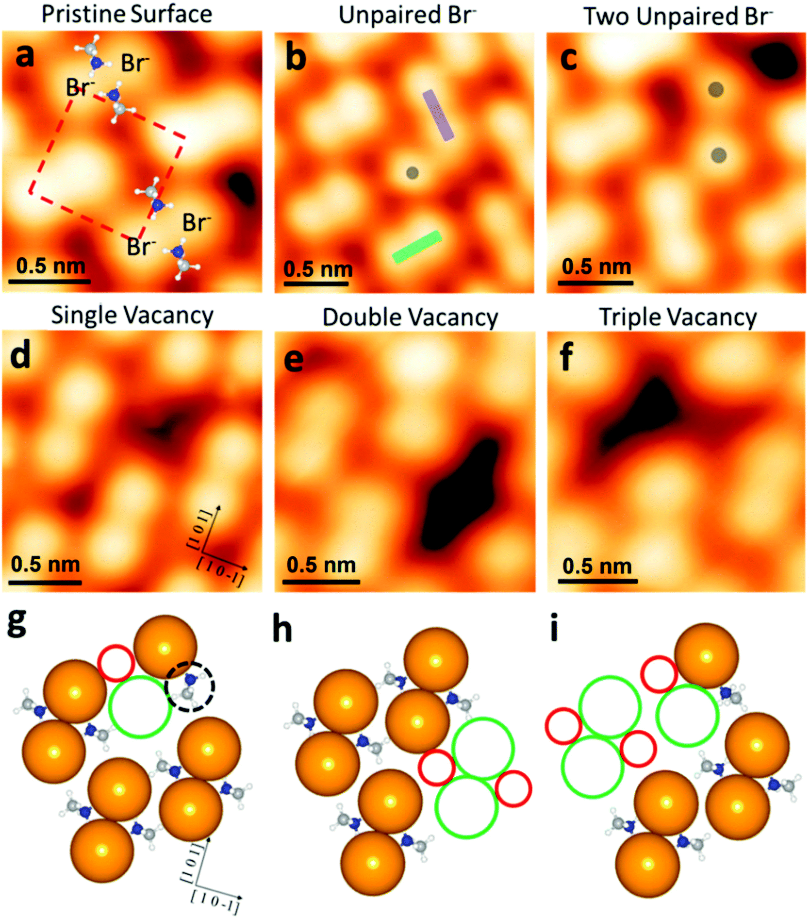 | ||
| Fig. 7 Intrinsic defects at the atomic scale on the surface of MAPbBr3. (a) STM image of the pristine MAPbBr3 surface, with MA+ molecules overlaid to show the relative position. The dashed red square denotes the unit cell of the MAPbBr3 (010) surface. (b) STM image of an unpaired Br− (gray dot) at the point where two Br-pair orientations (green and purple rectangles) meet. (c) STM image of two adjacent unpaired Br− (two gray dots), located near a vacancy. (d–f) STM images of single, double, and triple vacancy defects, respectively. (g–i) Top view of the model slab used for DFT defect formation energy calculations for the single, double, and triple vacancy defect cases, respectively. Solid green and red circles denote Br− and MA+ vacancy locations, respectively. The dashed black circle in (g) highlights a rotated MA+ molecule. (a–g) Reproduced with permission from ref. 63. | ||
The formation of double and triple MABr vacancies (Fig. 7h and i) was confirmed by the theoretical energy values. At the perovskite surface, the Br-pair reorientation is the main cause of the dynamics. The (010) surface was reconstructed by orienting the Br-pairs along either the (101) or (10−1) direction, which are orthogonal to each other (green and purple rectangles in Fig. 7b). Dissociation and re-association of the Br− pair with the neighboring Br ions might be the reason for this reconstruction. The MA+ rotation and Br− pair separation are also an important step for the occurrence of the Br− pair reorientation. This suggests that the reorientation event is more energetically favorable near a vacancy defect. An understanding of such defects at the perovskite surface or the heterojunction interface will enable direct utility in charge transport layers or electrodes of PV devices, since these have a direct impact on the charge carrier dynamics.
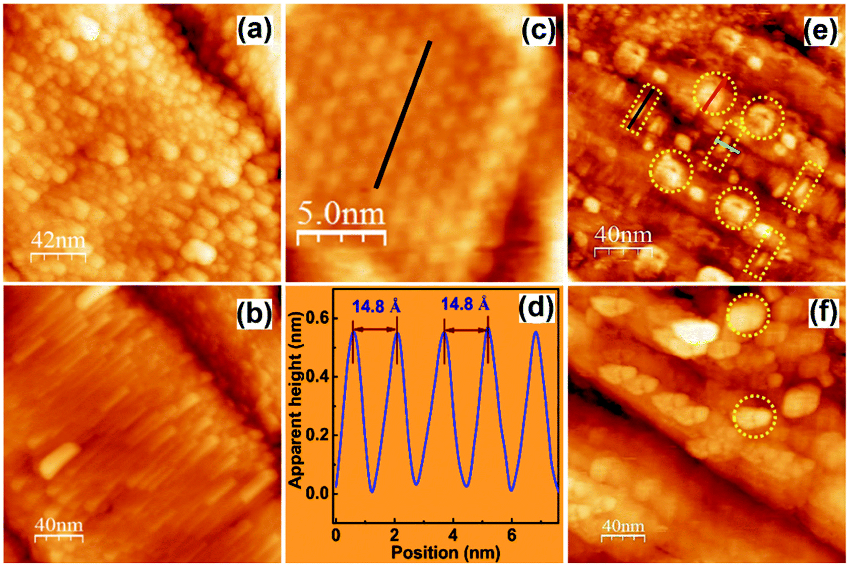 | ||
| Fig. 8 (a) Aged surfaces of an as-grown single crystal; (b) the pristine surfaces of a cleaved single crystal; (c) ordered structures of the pristine surface showing well-aligned stacked planes; (d) height profile of ‘c’ showing the Pb–Pb distance along the (110) plane; and (e and f) STM images of a pristine crystal showing the hydrate formation on the surface after overnight exposure to ambient air with ring-like protrusions (marked by circles) and the disunified 1D chains (marked by rectangles). (a–f) Reproduced with permission from ref. 84. | ||
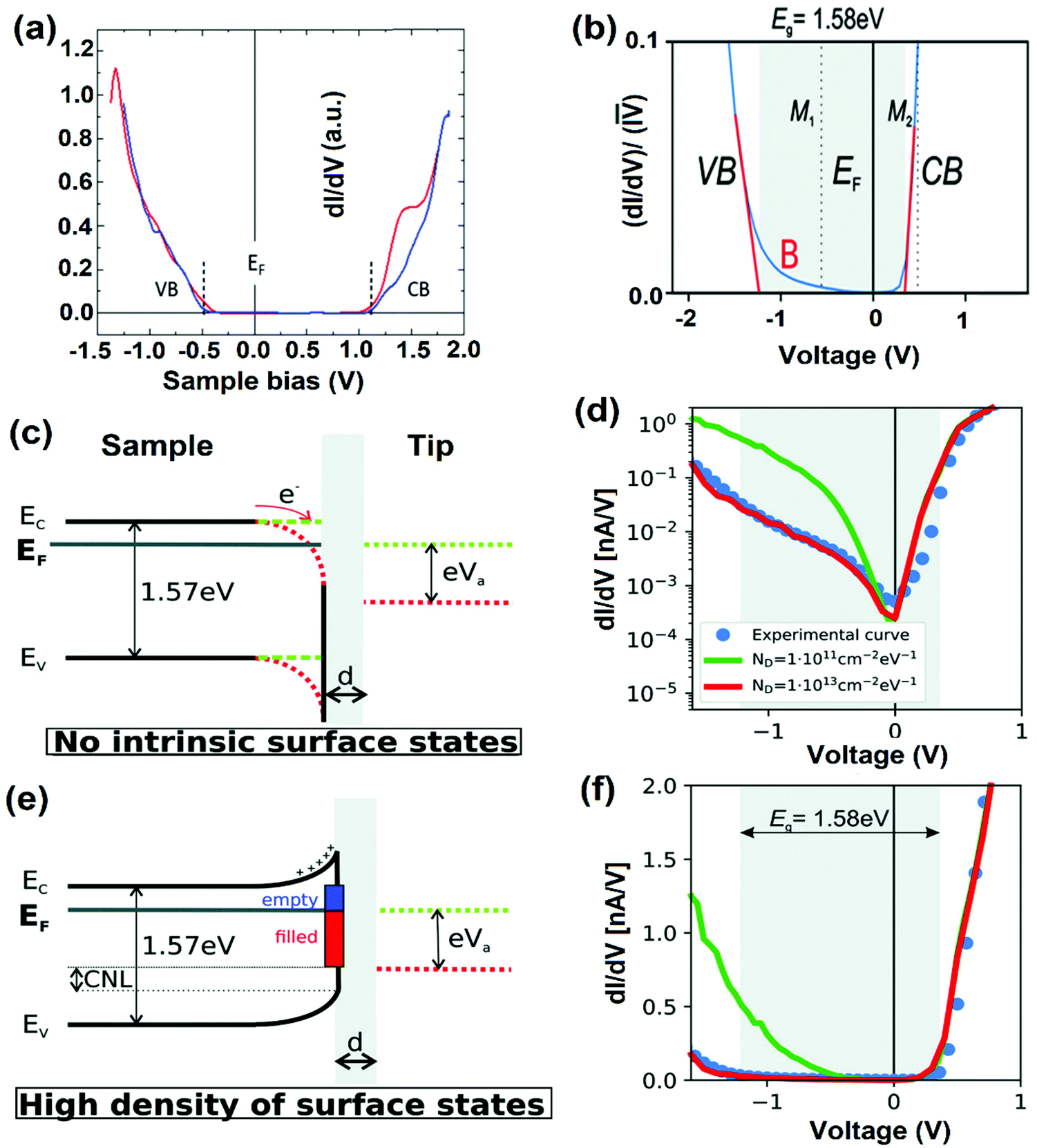 | ||
| Fig. 9 (a) STS of MAPbI3, where the dashed lines indicate the onset of the average conduction band (CB) and valence-band (VB). The STS shows that the material is a p-type semiconductor with an energy gap of 1.53 ± 0.05 eV. Reproduced with permission from ref. 58. (b) Averaged (dI/dV)/(I–V) curve. (c and e) The sketches of the tunneling junction between the surface and the tip without (c) and with high surface density states (e). (d and f) Simulated dI/dV curve on a logarithmic (d) and linear scale (f) for the two cases represented in (c) and (e), respectively. (b–f) Reproduced with permission from ref. 117. | ||
On the other hand, in the case of the high density of surface states, the charge neutrality level is lower than the EF level tending towards the negatively charged surface states, where upward band bending occurs (Fig. 9e). Under a positive bias, the tip-induced band bending does not occur due to the restrained EF level at the surface. Fig. 9d and f show the dI/dV spectra of two systems with no intrinsic surface state and with high surface density states on logarithmic and linear scales. At a small negative bias, tunneling conductance is low because of the high defect density of the surface leading to strong Fermi-level pinning. Tunneling can occur from the extended states of the VB, only when the applied bias is sufficiently negative. For these calculations, all-important parameters were considered to their highest accuracy. Such analyses are crucial, where different amounts of surface states occur due to the dissimilar surface terminations (due to exposure to air) or one type of facet that can dominate the band structure alterations.
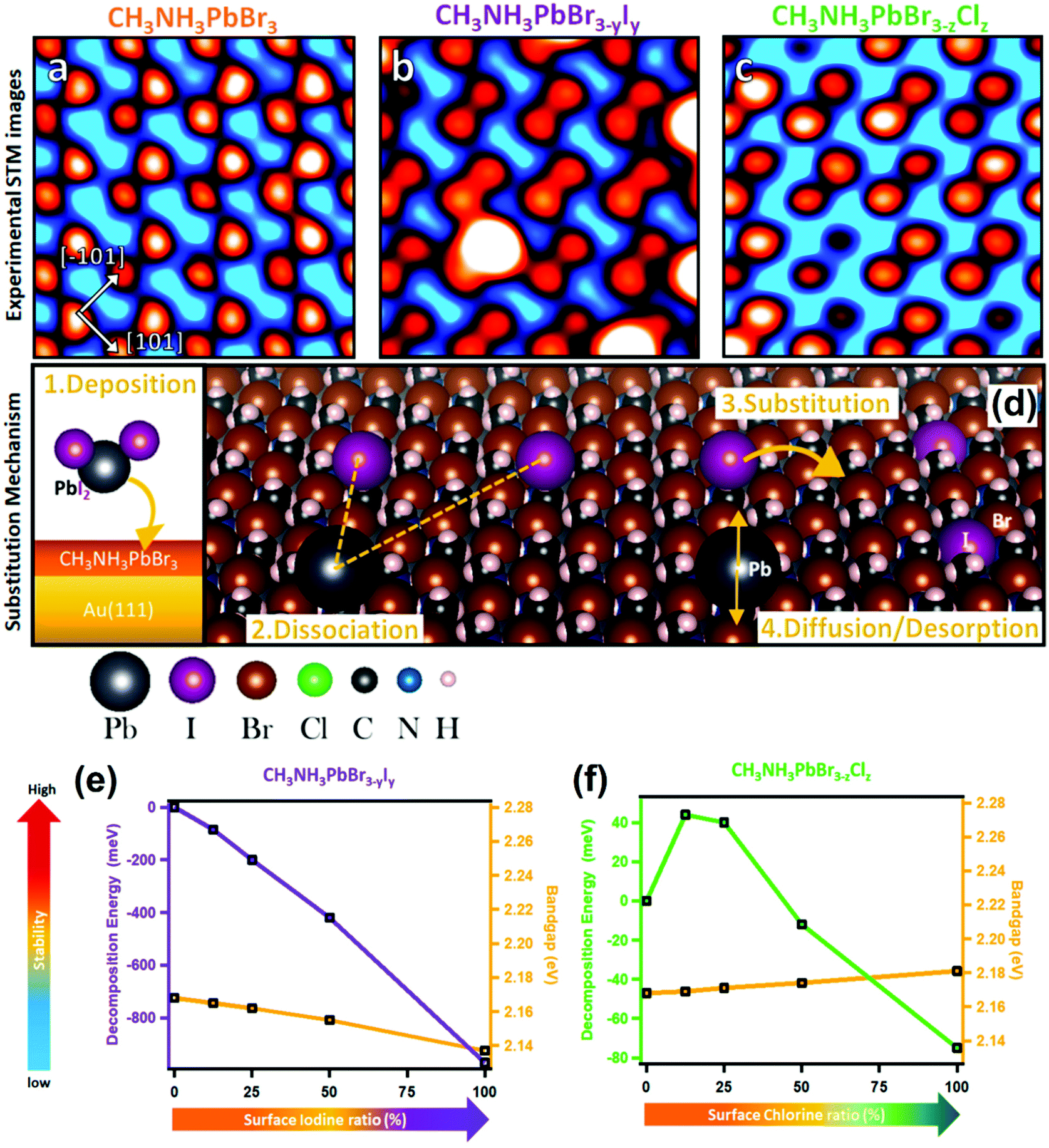 | ||
| Fig. 10 STM images of (a) MAPbBr3, (b) MAPbBr3−yIy, and (c) MAPbBr3−zClz with respect to halide substitution at the perovskite surface. (d) Scheme of the substitution mechanism occurring at the surface of the MAPbBr3 perovskite after deposition of PbI2 and PbCl2 molecules (only the PbI2 case is presented for clarity; however PbCl2 follows the same mechanism). Stability versus bandgap change in a mixed halide perovskite determined by DFT calculations: (e) MAPbBr3−yIy with increasing I content at the surface, and (f) MAPbBr3−zIz with increasing Cl content at the surface. (a–f) Reproduced with permission from ref. 125. | ||
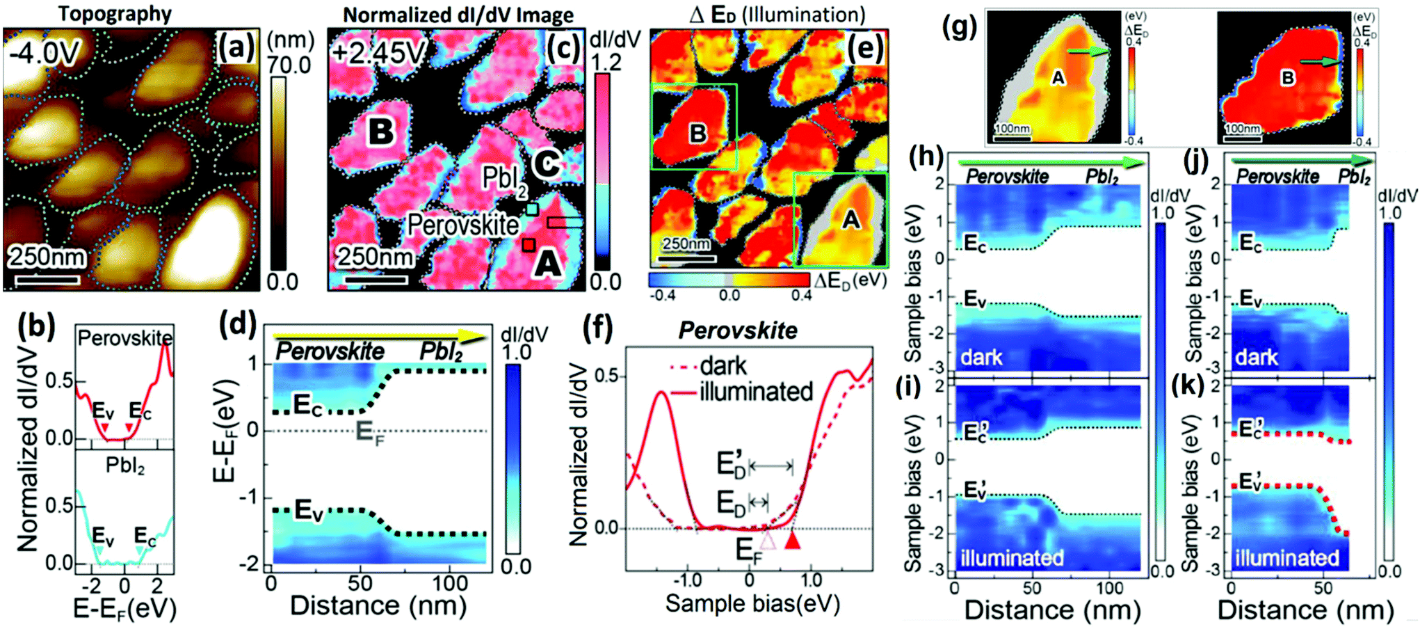 | ||
| Fig. 11 (a) Typical STM morphology image. (b) Two representative normalized dI/dV images of (c) (lower and upper panels) obtained at the outer part (blue square in grain A) and interior in the grain (red square in grain A), respectively. (c) A mapping image of the normalized dI/dV spectra of perovskite grains recorded at a sample bias of +2.45 V. (d) A mapping image of the band alignment across the MAPbI3/PbI2 hetero-interface in grain A by extracting the locations of the VB and CB edges. (e) A spatial distribution of ΔED values (ΔED = E′D − E) observed for the perovskite grains under light illumination. (f) Representative dI/dV curves of perovskites in the dark (dashed curve) and under light illumination (solid curve) conditions. (g) ΔED mapping of perovskite grains ‘A’ and ‘B’. (h) and (i) correspond to the band alignments across the heterojunctions of grain ‘A’ consisting of a thick (∼45 nm) PbI2 layer under darkness and light illumination, respectively. (j) and (k) correspond to the band alignments across the heterojunctions of grain ‘B’ consisting of a thin (∼8 nm) PbI2 layer under darkness and light illumination, respectively. (a–h) Reproduced with permission from ref. 48. | ||
The mapping image of the band alignment across the perovskite/PbI2 heterointerface in the grain is shown in Fig. 11d. The VB and CB edges for MAPbI3 and PbI2 were observed around 0.3 and 0.6 eV, respectively, which subsequently proves that the band alignment is of type I heterojunction at the perovskite/PbI2 interface. Additionally, the interior part of the MAPbI3 grain and PbI2 at the outer part of the grain behave as an intrinsic n-type semiconductor. Such STM/STS studies can directly help visualize spatially resolved band alignment characteristics and electronic configurations. Furthermore, under illumination, photoinduced charge transfer and band bending were observed at the heterostructure. The shift of the energy difference between the CB edge (EC) and the Fermi level (EF), denoted as ED = EC − EF, can be used to study the photoinduced characteristics of the material. Fig. 11f exhibits the difference between the CB edges (EC or E′C) and the Fermi level (EF) in a dark environment and under illumination, respectively. Under light illumination, the CB edge (EC, open red triangles) of the MAPbI3 part was shifted toward the higher energy (E′C, solid red triangular symbol). Also, light illumination effects cause an increase in LDOS, as observed in the dI/dV curve at a negative sample bias. This improved LDOS effect can be seen due to the increased tunneling current from the VB to the tip, which exhibits the carrier density enhancement of photoinduced holes in the MAPbI3 parts of the perovskite grains. Fig. 11e represents a light illuminated mapping image of the spatial distribution of ΔED observed for the perovskite grains, where ΔED values are obtained from the variation of ED and E′D. This variation is observed when photoexcited carriers are generated and are separated in the perovskite crystals under illumination. ΔED values in grain interiors were mostly positive (red or orange) and were either negative (blue) or nearly zero (gray) at the outer parts. This image typically shows the compositional distributions of MAPbI3 and PbI2 as shown in Fig. 11b. This study concludes that the chemical composition of perovskite grains plays a crucial role in the shifting of ΔED values and the charge transfer behaviors. In addition, the STS measurements show the consequences of the thin PbI2 layers on photocarrier generation and the separation at the heterointerface of perovskite crystal grains. Fig. 11g shows the ΔED band mapping across the perovskite/PbI2 heterojunctions of grains ‘A’ and ‘B’, and pointed with green colored arrows. The interfacial band alignments at grains A and B are shown in Fig. 11h–k. These band mapping was derived from the characteristic curves of the point-to-point STS data under the dark and illumination at both grains. In grain ‘B’, the PbI2 region showed a significant downward band bending, under illumination, whereas the energy shifts that occurred in the PbI2 region of grain A were not noteworthy. This result indicates that the transportation of photogenerated electrons was more efficient in the thinner layer of the PbI2 region of grain ‘B’. On the other hand, the thick PbI2 layer in grain ‘A’ affects the photoinduced charge transfer and probability of carrier recombination. Consequently, under light illumination, the hole concentration increases in the inner area of grain ‘A’ compared to that of grain ‘B’. Grain ‘A’ exhibited shifting of VB and CB edges by ∼ 0.25 eV toward high energy (Fig. 11i); and an ∼0.40 eV shift occurred in the perovskite region of grain ‘B’ (Fig. 11k). This thickness dependent variation in the energy level shift may be due to the non-uniform decomposition of MAPbI3 during thermal annealing.131 This study reveals the important role of the PbI2 passivation layers in the perovskite crystal grains. The unique LM-STM technique enables us to study photocarrier generation and interfacial electronic structures under the spatially resolved conditions offering great potential for exploration in PV and photochemical cells.
3.2. Cesium based halide perovskites
As the hybrid perovskite materials were developed for PV applications, atoms of cesium (Cs), Rb+, europium (Eu), etc. have also been introduced as cations in perovskite structures.132–135 The main goal of incorporating such metals into solar cells is not only to improve the efficiency, but also to increase the stability of the materials/device. Many groups have carried out numerous experiments on inorganic perovskites such as CsPbBr3,136,137 Cs2InAgCl6,138 Cs2AgBiBr6,139 and Cs2TiBr6.140 Among them, CsPbBr3 is known as a highly defect tolerant material in terms of its electronic structure, and the secret of perovskite stability lies in the structure.141 Most of the inherent defects lead to shallow transition levels, though a few of them may create deep transition levels with greater formation energies. Hence, CsPbBr3 can maintain its good electronic quality despite the presence of defects.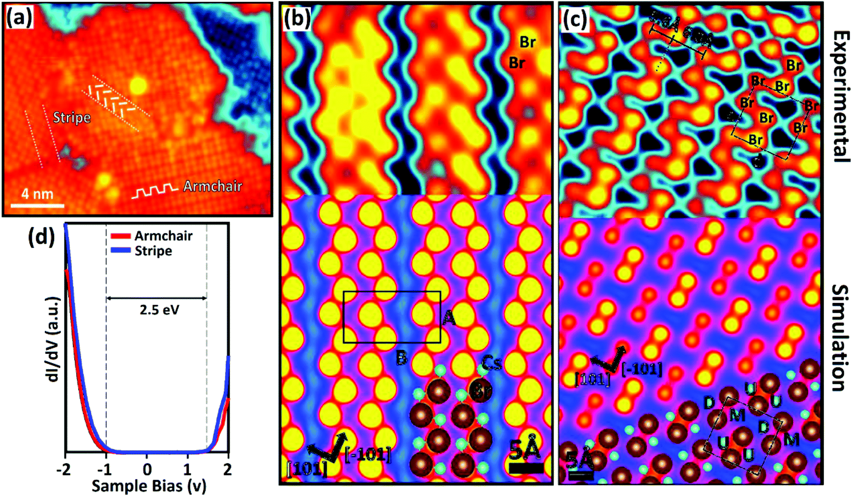 | ||
| Fig. 12 (a) Topographic image of the CsPbBr3 film obtained by STM: a “stripe” domain and an “armchair” domain indicated by the white segments; experimental image and simulated model of STM. (b) The stripe reconstruction of CsPbBr3 and (c) the armchair reconstruction of CsPbBr3. The black rectangle in ‘b’ indicates the unit-cell of the stripe structure. The black square in ‘c’ represents the unit-cell of the armchair structure. (d) Local band structure determination of the CsPbBr3 perovskite for the stripe and armchair domains. (a–d) Reproduced with permission from ref. 142. | ||
The DFT model shows the evaluation of the CsPbBr3 stripe domain reconstruction, which occurred due to the alternation of the short (6.2 Å) and long (7.8 Å) spacing between the Br pairs (Fig. 12b). These calculations have disclosed the formation of Br pairs due to the coulombic interaction between the Br ion and two nearby Cs cations. In contrast, the reconstruction of the armchair domain (Fig. 12c) arises from the alternation of bright and dark Br pair rows that originates from a change in the vertical position of surface ions. The armchair unit cell consists of four Br anions and four Cs cations, and is similar to the stripe domain shown in Fig. 12c (black square). Furthermore, it demonstrated that the armchair domain is less energetically favorable than the stripe domain that has a more compact nature. For both cases, DFT calculation results matched well with the experimental results. The electronic properties (STS) of the CsPbBr3 perovskite were determined independently in the stripe and armchair domains, as shown in Fig. 12d. Interestingly, the electronic properties for the stripe and armchair domains are quite similar irrespective of their significant structural differences. The evaluation of two surface structures due to the complex coulombic interactions between Cs and Br in CsPbBr3 could pave the way for understanding the stability deeply. Similarly, accurate band structure resolution could allow better prediction of interfacial properties.
3.3. Oxide perovskites
Oxide perovskite materials exhibit a wide range of attractive properties including superconducting, ferroelectric, magneto-resistive, and PV properties due to their structural and compositional flexibility.100,143 This section is constructed within the scope of local morphological and spectroscopic information of oxide perovskite materials such as BaTiO3, BiFeO3, Pb(Zr,Ti)O3, etc., which are actually being used as a photo-active or charge-transport layer in PV devices.144–149 Such perovskite materials possess peculiar ferroelectric properties, which can provide an effective driving force for charge generation and separation due to the strong intrinsic dipoles. Numerous theories have been proposed for probing the origin of this intriguing phenomenon. However, as far as the PV effect is concerned, it is difficult to figure out a single unified theory that can explain oxide perovskites with various forms.150,151Recently, Bi2FeCrO6-based heterojunction devices have been demonstrated to reach 2% photoconversion efficiency (PCE).152 Similarly, several groups have performed numerous experiments on solar cells based on oxide perovskites such as BiFeO3,153 Pb(Zr,Ti)O3 (PZT),154 and BaTiO3155; however, all of them have shown very low PCE. Low PCEs are presumably due to the very low short-circuit current-density (Jsc) in the range of μA–mA cm−2, which cannot be determined by the large bandgap of absorbers. For instance, BiFeO3 has a relatively small bandgap, and shows absorption only in the visible region.156 However, other BiFeO3-based perovskite devices possess a relatively larger bandgap, exhibiting Jsc in the range of 1–1.5 mAcm−2.147 Therefore, the efficiency enhancement in oxide perovskite-based devices is a difficult and challenging arena to work upon. Furthermore, researchers are still sorting out challenges by analyzing local energy levels along with the charge transfer phenomenon and morphology. The electronic structure of a SrTiO3 perovskite has been visualized by Hitosugi et al.,157 and its PV performance is demonstrated by Wu et al.158 The defect states owing to oxygen vacancies have been observed in the synthesized perovskite through the spatial distribution in electronic structures. These results can be useful to predict the performance of the device, since mostly defect states are responsible for hysteresis generation in the I–V characteristics of solar cells that affect its overall performance. Cai et al. have identified the temperature-dependent properties in a La0.8Sr0.2CoO3 (LSCO) perovskite from surface electronic structures, where the transition occurred from the semiconducting to metallic states.159 In brief, they explored the influence of temperature and lattice strain on the surface electronic structure. Both the tensile and compressive strained LSCO (on SrTiO3 crystal) surfaces can alter a semiconducting state (at room temperature) to a metal-like state (at elevated temperatures) captured by in situ STS.
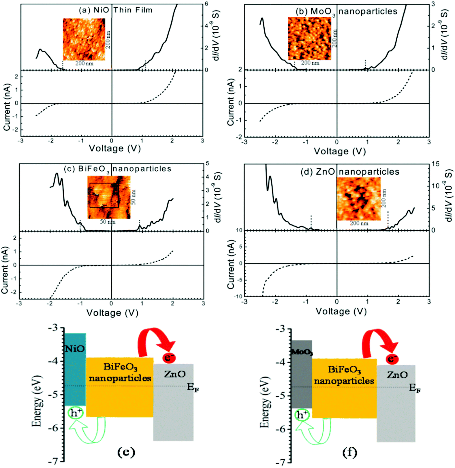 | ||
| Fig. 13 Current–voltage and density of states (dI/dV) plots of (a) a NiO thin film and (b) MoO3 (c) BiFeO3 and (d) ZnO nanoparticles. STM topography of the active layer is shown in the inset of each figure. Schematic description of the energy level diagrams of (e) NiO–BiFeO3–ZnO and (f) MoO3–BiFeO3–ZnO heterojunctions. (a–f) Reproduced with permission from ref. 160. | ||
In the DOS spectra, the valence band's position with respect to Fermi energy decided the p-type nature of NiO and MoO3 (Fig. 13a and b), and the n-type nature of ZnO (Fig. 13d) nanocrystal semiconductors. The DOS spectrum of BiFeO3 NPs showed an intrinsic semiconductor characteristic (Fig. 13c). The detailed analysis of the band edges of NiO, MoO3, BiFeO3, and ZnO NPs showed both the developed structures, i.e. NiO–BiFeO3–ZnO and MoO3–BiFeO3–ZnO heterojunctions would form p–i–n structures with a type-II band alignment at both the interfaces (Fig. 13e and f). These kinds of heterojunctions can further be very efficient at quick charge separation within their charge carrier lifetime when used in PV materials. Subsequently, these materials can become proficient in the PV arena.
Fig. 14a and b exhibit the surface morphological view of sample-I and sample-II. Sample-I showed spherical and densely packed individual grains; whereas sample-II showed continuous film formation with irregular grains and their broad size distribution. Fig. 14c and d depict comparative dI/dV curves of sample-I and sample-II on the grain and grain boundaries that generate a picture of LDOS near the Fermi energy of the samples. The difference in dI/dV curves at two different locations (i.e. on the grain and at the grain boundaries) reflected the coexistence of conducting and insulating regions. This difference typically depended upon the position of the grain boundary and it was more prominent in sample-II than in sample-I. Sample-I showed a firm morphology and hence the presence of more systematic semiconducting regions. In this finding, two types of typical characteristics of both films were studied. Firstly, a linear region at the Fermi energy, corresponding to the metallic phase, and other plateau regions that signify the presence of a semiconducting gap in both samples were observed. Sample-II showed a small shift in the pseudogap as compared to sample-I. However, the grain boundary defines the presence of a semiconducting gap. In comparison with sample-I, the gap increases in sample-II. Sample-I showed more prominent grain boundary distribution, where this kind of semiconducting grain boundary can be well situated for device applications.
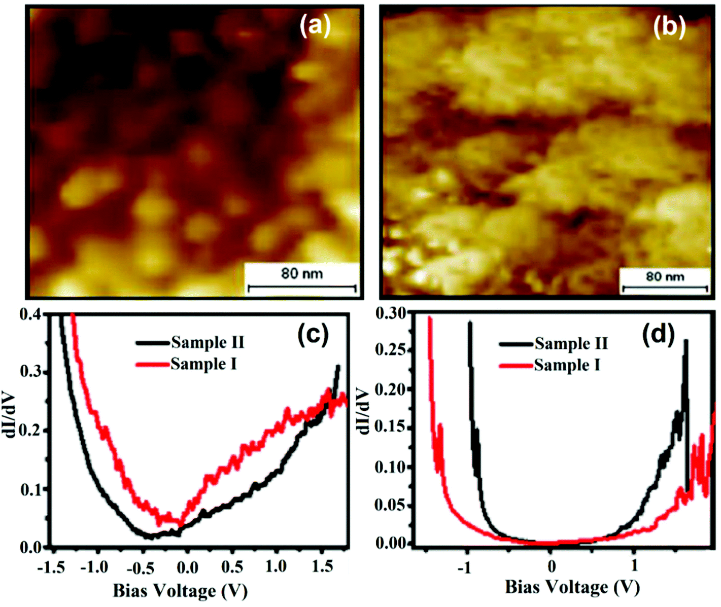 | ||
| Fig. 14 Recorded topographic STM images of (a) sample-I: La0.7Sr0.3MnO with a packed-island and (b) sample-II: La0.7Sr0.3MnO with a smooth morphology; comparison of dI/dV of sample-I and sample-II (c) on the grain and (d) on the grain boundary. (a–d) Reproduced with permission from ref. 65. | ||
LCMO (LaxCa1−xMnO3) also presents some PV properties with different heterostructures studied by various groups.167–170 Wei et al. have demonstrated the PV effect in La0.67Ca0.33MnO3/LaMnO3/Nb:SrTiO3 hetero-junctions, where the PV response has been observed to improve significantly as the film thickness increases from 5 to 50 nm (saturates above 50 nm), and Ni et al. investigated the transient PV properties of La0.4Ca0.6MnO3/Nb:SrTiO3 hetero-junctions for a wide range of temperatures from 293 to 723 K.168 They observed that the oxygen vacancies may exist in LCMO thin films during deposition at different temperatures, leading to the variation in the I–V characteristics. Furthermore, they have explained the transient photo-response with the help of an LCMO/NSTO junction under applied biases. Upon applying a positive bias to the LCMO thin films, positively charged oxygen vacancies transfer from LCMO to the LCMO/NSTO interface and form an interface barrier. Near the interface, highly oxygen-deficient LCMO experiences a wide bandgap that can be an effective barrier for the conduction of charge carriers. The surface oxygen stoichiometry in LCMO has been studied in detail via STM/STS to obtain more insights into both chemical (e.g. surface electrochemistry) and physical (e.g. LDOS, band structure, etc.) properties.171 La0.625Ca0.375MnO3 thin films on SrTiO (001) have also been investigated through in situ STM, in a real-time fashion. They demonstrated the ability to form oxygen vacancies along with the removal and deposition of individual atomic units under different potential stresses. These studies can help us understand the surface reactions in perovskite systems.
4. Conclusion and outlook
The morphology and local electronic properties of the materials are highly correlated with their relevant physical, chemical, and electronic parameters, which in turn affect the device performance, for example of solar cells. While traditional imaging techniques such as SEM, AFM, and TEM can offer excellent information about the quality, roughness, and thickness of thin films, all of them lack the ability to identify different materials that in general are binary components in solar cells. In this regard, STM/STS based on its unique operation principle presents the powerful ability in terms of many aspects. With STS/STS, the electronic states of materials can be readily analyzed at nanoscale precision. For example: (i) the band diagram of solar cells can be drawn based on the aspect of charge carriers in a device; (ii) the band alignment in a junction of a PV device can be drawn before actually incorporating into a device; and (iii) the dI/dV function in STM/STS can reveal the energetic mapping domains of the heterojunction of the energy maps of different materials. KPFM is basically an AFM mode, and functions in the similar way of STM/STS. However, STM/STS obtains electronic spectroscopy from the LDOS for the target materials presenting a relatively much more straightforward manner in analytical propose. Besides it, the tips of STM are easier to prepare compared with those of AFM (e.g., by just mechanically cutting a metal wire, typically either Pt/Ir or tungsten).As mentioned earlier, we have witnessed the unprecedented power of STM/STS in analyses of energy materials. We have thus reviewed recent examples to strengthen the basic understanding of the structural studies of both oxide and halide perovskite materials by using the STM/STS technique in conjunction with their related applications in solar cells. In particular, STM/STS among other analytical tools stands out as a complementary means to unveil the unique information of materials at the atomic and electronic levels. It allows in situ measurements capable of real-time monitoring of the growth and evolution of materials-formation processes. A sample with an atomically flat surface is a requirement in STM analysis, facilitating in-depth and clear electronic information. Different deposition techniques lead to the formation of surface defects in a crystal or during thin-film formation. As reviewed, the cleaving method is also known as X-STM, which has been used for sample preparation from single-crystals for STM observations. In addition, samples can also be deposited through spin coating and CVD techniques. Sometimes, the samples prepared by spin coating and CVD techniques may need further processes using a cleaving method, subject to the requirement of the sample for the cross-sectional interfacial study.
The STM/STS techniques can provide an in-depth understanding of the stability, charge carrier dynamics, and other optoelectronic conversion-related properties at heterojunction interfaces of materials. For the halide perovskites, STM/STS studies of the MAPbBr3 electronic structure reveal the contribution of Br and MA orbitals for the electron density states on the perovskite surface along with the real-time view of dislocation and intrinsic defects in a single crystal. Such results are crucial for understanding the behavior of the halide perovskite surfaces at the atomic scale, where the orientation of MA modifies the dipole strength and hence the stability of the structure. The various kinds of defects such as, cationic, anionic, excess halide, and antisite defects on the perovskite surface affect the band structure and the local work function, which will further alter the charge carrier dynamics, lifetime and subsequent recombination at the interface of the heterojunctions. Such surface and energy levels related to systematic STM/STS analysis can directly correlate the atomic interface phenomenon with the device performance from the perspective of defects and interface engineering.
The mixing of halides provides stability to the hybrid perovskites under specific moisture, temperature, and light conditions. For example, the amount of variation in I and Cl concentrations as a part of MAPbBr3 depicts the stability without a destructive band gap alteration, which further provides a conclusive direction for the fabrication of stable and efficient hybrid perovskite PV devices. These studies offer convincing responses to the current discussion in the world energy forum on halide variation or incorporation in hybrid perovskites for durable large-scale devices. CsPbBr3 has become a novel halide perovskite material in the PV domain due to its nearly defect-free nature and improved stability. Even structurally different forms of CsPbBr3 also show quite similar electronic properties. Furthermore, this tool has been used to explore oxide perovskites that bear ferroelectric properties, believed to carry dynamic force for the charge carrier generation and extraction mechanism due to the strong intrinsic dipole interactions. The rapid movement of charges enhances the open-circuit voltage in the PV devices, and hence the overall performance. These literature reports provide important information regarding the stability improvement of the materials and the efficiency enhancement of the corresponding devices, based on their structural properties such as compositions, defects, vacancies, and terminations of the structure. Upon studying these structural properties, one can follow a similar theoretical approach for studying an atom experimentally to its utmost depth. To this end, STM stands out as the best technique. Along this direction, further research efforts should focus on defect tolerance and its origins, which will help researchers design new materials with better defect tolerance, higher stability, and minimal toxicity. We expect that the in situ atomic and electronic visualizations of the real-time sample preparation and their time-dependent evolution through STM works will pave the way for uncovering numerous crucial and puzzling phenomena in oxide and halide perovskites, such as ion/charge carrier migration, hysteresis, and the stability mechanism, eventually enabling commercialization of PVs soon.
Conflicts of interest
There are no conflicts to declare.Acknowledgements
The authors thank NSFC (21972095), Shenzhen University, Guangdong government (2018A030313467), Shenzhen city (1. the overseas talent set-up funding; 2. exploring multicomponent supramolecular systems, JCYJ20180305124732178; and 3. Shenzhen University and National Taipei University of Technology joint funding (2019008)). China's Postdoctoral Science Foundation (65th Batch-2019M653033). The authors thank Prof. Steven De Feyter (K. U. Leuven) for his grateful discussion with us in this review.References
- W. Q. Wu, Q. Wang, Y. Fang, Y. Shao, S. Tang, Y. Deng, H. Lu, Y. Liu, T. Li, Z. Yang and A. Gruverman, Nat. Commun., 2018, 9, 1625 CrossRef PubMed.
- D. Zhao, C. Wang, Z. Song, Y. Yu, C. Chen, X. Zhao, K. Zhu and Y. Yan, ACS Energy Lett., 2018, 3, 305 CrossRef CAS.
- D. W. De Quilettes, K. Frohna, D. Emin, T. Kirchartz, V. Bulovic, D. S. Ginger and S. D. Stranks, Chem. Rev., 2019, 119, 11007 CrossRef CAS PubMed.
- J. Shi, Y. Wang and Y. Zhao, Energy Environ. Mater., 2019, 2, 73 CrossRef CAS.
- R. Lin, K. Xiao, Z. Qin, Q. Han, C. Zhang, M. Wei, M. I. Saidaminov, Y. Gao, J. Xu, M. Xiao and A. Li, Nat. Energy, 2019, 4, 864 CrossRef CAS.
- S. A. Veldhuis, P. P. Boix, N. Yantara, M. Li, T. C. Sum, N. Mathews and S. G. Mhaisalkar, Adv. Mater., 2016, 28, 6804 CrossRef CAS PubMed.
- C. Li, S. Cong, Z. Tian, Y. Song, L. Yu, C. Lu, Y. Shao, J. Li, G. Zou, M. H. Rümmeli and S. Dou, Nano Energy, 2019, 60, 247 CrossRef CAS.
- X. Yang, L. F. Ma and D. Yan, Chem. Sci., 2019, 10, 4567 RSC.
- J. Lu, X. Lin, X. Jiao, T. Gengenbach, A. D. Scully, L. Jiang, B. Tan, J. Sun, B. Li, N. Pai and U. Bach, Energy Environ. Sci., 2018, 11, 1880 RSC.
- B. Parida, S. Yoon, S. M. Jeong, J. S. Cho, J. K. Kim and D. W. Kang, Sol. Energy Mater. Sol. Cells, 2020, 204, 110212 CrossRef CAS.
- Q. Wali, F. J. Iftikhar, N. K. Elumalai, Y. Iqbal, S. Yousaf, S. Iqbal and R. Jose, Curr. Appl. Phys., 2020, 20, 720 CrossRef.
- Z. Wang, Y. Gu, J. Qi, S. Lu, P. Li, P. Lin and Y. Zhang, RSC Adv., 2015, 5, 42075 RSC.
- P. L. Qin, H. W. Lei, X. L. Zheng, Q. Liu, H. Tao, G. Yang, W. J. Ke, L. B. Xiong, M. C. Qin, X. Z. Zhao and G. J. Fang, Adv. Mater. Interfaces, 2016, 3, 1500799 CrossRef.
- B. Yang, C. C. Brown, J. Huang, L. Collins, X. Sang, R. R. Unocic, S. Jesse, S. V. Kalinin, A. Belianinov, J. Jakowski and D. B. Geohegan, Adv. Funct. Mater., 2017, 27, 1700749 CrossRef.
- T. Bu, X. Liu, Y. Zhou, J. Yi, X. Huang, L. Luo, J. Xiao, Z. Ku, Y. Peng, F. Huang and Y. B. Cheng, Energy Environ. Sci., 2017, 10, 2509 RSC.
- C. Li, S. Tscheuschner, F. Paulus, P. E. Hopkinson, J. Kießling, A. Köhler, Y. Vaynzof and S. Huettner, Iodine migration and its effect on hysteresis in perovskite solar cells, Adv. Mater., 2016, 28, 2446 CrossRef CAS PubMed.
- T. S. Sherkar, C. Momblona, L. Gil-Escrig, J. ávila, M. Sessolo, H. J. Bolink and L. J. A. Koster, ACS Energy Lett., 2017, 2, 1214 CrossRef CAS PubMed.
- J. H. Lee, J. Kim, G. Kim, D. Shin, S. Y. Jeong, J. Lee, S. Hong, J. W. Choi, C. L. Lee, H. Kim and Y. Yi, Energy Environ. Sci., 2018, 11, 1742 RSC.
- J. Kim, B. W. Park, J. Baek, J. S. Yun, H. W. Kwon, J. Seidel, H. Min, S. Coelho, S. Lim, S. Huang and K. Gaus, J. Am. Chem. Soc., 2020, 142, 6251 CrossRef CAS PubMed.
- S. A. Kulkarni, S. G. Mhaisalkar, N. Mathews and P. P. Boix, Small, 2019, 3, 1800231 CrossRef.
- M. Saliba, J. P. Correa-Baena, M. Grätzel, A. Hagfeldt and A. Abate, Angew. Chem., Int. Ed., 2018, 57, 2554 CrossRef CAS PubMed.
- M. Long, T. Zhang, M. Liu, Z. Chen, C. Wang, W. Xie, F. Xie, J. Chen, G. Li and J. Xu, Adv. Mater., 2018, 30, 1801562 CrossRef PubMed.
- X. Zhu, J. Lee and W. D. Lu, Adv. Mater., 2017, 29, 1700527 CrossRef PubMed.
- X. Zheng, Y. Deng, B. Chen, H. Wei, X. Xiao, Y. Fang, Y. Lin, Z. Yu, Y. Liu, Q. Wang and J. Huang, Adv. Mater., 2018, 30, 1803428 CrossRef PubMed.
- M. Chen, M. G. Ju, H. F. Garces, A. D. Carl, L. K. Ono, Z. Hawash, Y. Zhang, T. Shen, Y. Qi, R. L. Grimm and D. Pacifici, Nat. Commun., 2019, 10, 16 CrossRef CAS PubMed.
- M. B. Islam, M. Yanagida, Y. Shirai, Y. Nabetani and K. Miyano, Sol. Energy Mater. Sol. Cells, 2019, 195, 323 CrossRef CAS.
- Y. J. Chen, M. J. Zhang, S. Yuan, Y. Qiu, X. B. Wang, X. Jiang, Z. Gao, Y. Lin and F. Pan, Nano Energy, 2017, 36, 303 CrossRef CAS.
- C. S. Kley, C. Dette, G. Rinke, C. E. Patrick, J. Čechal, S. J. Jung, M. Baur, M. Dürr, S. Rauschenbach, F. Giustino and S. Stepanow, Nano Lett., 2014, 14, 563 CrossRef CAS PubMed.
- S. Rößler, B. Padmanabhan, S. Elizabeth, H. L. Bhat, F. Steglich and S. Wirth, Appl. Phys. Lett., 2010, 96, 202512 CrossRef.
- Y. Almadori, D. Moerman, J. L. Martinez, P. Leclère and B. Grévin, Beilstein J. Nanotechnol., 2018, 9, 1695 CrossRef CAS PubMed.
- C. Wang, C. Zhang, S. Tong, J. Shen, C. Wang, Y. Li, S. Xiao, J. He, J. Zhang, Y. Gao and J. Yang, J. Phys. Chem. C, 2017, 121, 6575 CrossRef CAS.
- J. J. Li, J. Y. Ma, Q. Q. Ge, J. S. Hu, D. Wang and L. J. Wan, ACS Appl. Mater. Interfaces, 2015, 7, 28518 CrossRef CAS PubMed.
- R. Kumar, D. Varandani and B. R. Mehta, Carbon, 2016, 98, 41 CrossRef CAS.
- B. Huang, G. Kong, E. N. Esfahani, S. Chen, Q. Li, J. Yu, N. Xu, Y. Zhang, S. Xie, H. Wen and P. Gao, npj Quantum Mater., 2018, 3, 30 CrossRef.
- M. Cai, N. Ishida, X. Li, X. Yang, T. Noda, Y. Wu, F. Xie, H. Naito, D. Fujita and L. Han, Joule, 2018, 2, 296 CrossRef CAS.
- T. Glatzel, S. Sadewasser and M. C. Lux-Steiner, Appl. Surf. Sci., 2003, 210, 84 CrossRef CAS.
- W. Li, M. U. Rothmann, A. Liu, Z. Wang, Y. Zhang, A. R. Pascoe, J. Lu, L. Jiang, Y. Chen, F. Huang and Y. Peng, Adv. Energy Mater., 2017, 7, 1700946 CrossRef.
- M. M. Tavakoli, M. Saliba, P. Yadav, P. Holzhey, A. Hagfeldt, S. M. Zakeeruddin and M. Grätzel, Adv. Energy Mater., 2019, 9, 1802646 CrossRef.
- D. Kim, J. H. Yun, M. Lyu, J. Kim, S. Lim, J. S. Yun, L. Wang and J. Seidel, J. Phys. Chem. C, 2019, 23, 14144 CrossRef.
- S.-L. Lee, N.-T. Lin, C.-H. Chen, H.-C. Yang and T.-Y. Luh, Chem. – Eur. J., 2009, 15, 11594 CrossRef CAS PubMed.
- J. R. O'Dea, L. M. Brown, N. Hoepker, J. A. Marohn and S. Sadewasser, MRS Bull., 2012, 37, 642 CrossRef.
- G. Binnig, H. Rohrer, C. Gerber and E. Weibel, Phys. Rev. Lett., 1982, 49, 57 CrossRef.
- M. Saeed, A. Mahmood, A. S. Saleemi, X. Zeng and S. L. Lee, J. Phys. Chem. C, 2020, 124, 829 CrossRef CAS.
- U. Dasgupta, A. Bera and A. J. Pal, ACS Energy Lett., 2017, 2, 582 CrossRef CAS.
- R. Ohmann, L. K. Ono, H. S. Kim, H. Lin, M. V. Lee, Y. Li, N. G. Park and Y. Qi, J. Am. Chem. Soc., 2015, 137, 16049 CrossRef CAS PubMed.
- L. She, M. Liu and D. Zhong, Atomic structures of CH3NH3PbI3 (001) surfaces, ACS Nano, 2015, 10, 1126 CrossRef PubMed.
- T. Hitosugi, R. Shimizu and T. Ohsawa, et al. , Chem. Rec., 2014, 14, 935 CrossRef CAS PubMed.
- M. C. Shih, S. S. Li, C. H. Hsieh, Y. C. Wang, H. D. Yang, Y. P. Chiu, C. S. Chang and C. W. Chen, Nano Lett., 2017, 17, 1154 CrossRef CAS PubMed.
- C. Renner, G. Aeppli and H. M. Ronnow, Mater. Sci. Eng., C, 2005, 25, 775 CrossRef.
- N. D. Desai, V. B. Ghanwat, K. V. Khot, S. S. Mali, C. K. Hong and P. N. Bhosale, J. Mater. Sci.: Mater. Electron., 2016, 27, 2385 CrossRef CAS.
- T. Dimopoulos, M. Bauch, R. A. Wibowo, N. Bansal, R. Hamid, M. Auer, M. Jäger and E. J. W. List-Kratochvil, Mater. Sci. Eng., B, 2015, 200, 84 CrossRef CAS.
- A. Fujiki, Y. Miyake, Y. Oshikane, M. Akai-Kasaya, A. Saito and Y. Kuwahara, Nanoscale Res. Lett., 2011, 6, 1 CrossRef PubMed.
- A. Sasaki, F. Iwata, A. Katsumata, T. Akiyama and H. Fujiyasu, Rev. Sci. Instrum., 1997, 68, 1296 CrossRef CAS.
- L. She, M. Liu, X. Li, Z. Cai and D. Zhong, Surf. Sci., 2017, 656, 17 CrossRef CAS.
- M. Graetzel, R. A. Janssen, D. B. Mitzi and E. H. Sargent, Nature, 2012, 488, 304 CrossRef CAS PubMed.
- H. L. Hsu, C. P. Chen, J. Y. Chang, Y. Y. Yu and Y. K. Shen, Nanoscale, 2014, 6, 10281 RSC.
- L. Dou, A. B. Wong, Y. Yu, M. Lai, N. Kornienko, S. W. Eaton, A. Fu, C. G. Bischak, J. Ma, T. Ding and N. S. Ginsberg, Science, 2015, 349, 1518 CrossRef CAS PubMed.
- D. Azulay, I. Levine, S. Gupta, E. Barak-Kulbak, A. Bera, G. San, S. Simha, D. Cahen, O. Millo, G. Hodes and I. Balberg, Phys. Chem. Chem. Phys., 2018, 20, 24444 RSC.
- A. J. Yost, A. Pimachev, C. C. Ho, S. B. Darling, L. Wang, W. F. Su, Y. Dahnovsky and T. Chien, ACS Appl. Mater. Interfaces, 2016, 8, 29110 CrossRef CAS PubMed.
- S. Wang, L. K. Ono, M. R. Leyden, Y. Kato, S. R. Raga, M. V. Lee and Y. Qi, J. Mater. Chem. A, 2015, 3, 14631 RSC.
- M. Liu, M. B. Johnston and H. J. Snaith, Nature, 2013, 501, 395 CrossRef CAS PubMed.
- O. Malinkiewicz, A. Yella, Y. H. Lee, G. M. Espallargas, M. Graetzel, M. K. Nazeeruddin and H. J. Bolink, Nat. Photonics, 2014, 8, 128 CrossRef CAS.
- C. Stecker, K. Liu, J. Hieulle, R. Ohmann, Z. Liu, L. K. Ono, G. Wang and Y. Qi, ACS Nano, 2019, 13, 12127 CrossRef CAS PubMed.
- C. W. Chen, H. W. Kang, S. Y. Hsiao, P. F. Yang, K. M. Chiang and H. W. Lin, Adv. Mater., 2014, 26, 6647 CrossRef CAS PubMed.
- A. Joshi, R. Nori, S. Dhobale, V. R. Rao, S. N. Kale and S. Datar, Phys. B, 2014, 448, 85 CrossRef CAS.
- M. M. Tavakoli, L. L. Gu, Y. Gao, C. Reckmeier, J. He, A. L. Rogach, Y. Yao and Z. Y. Fan, Fabrication of efficient planar perovskite solar cells using a one-step chemical vapor deposition method, Sci. Rep., 2015, 5, 1408 Search PubMed.
- M. R. Leyden, M. V. Lee, S. R. Raga and Y. B. Qi, J. Mater. Chem. A, 2015, 3, 16097 RSC.
- J. Ávila, C. Momblona, P. P. Boix, M. Sessolo and H. J. Bolink, Joule, 2017, 1, 431 CrossRef.
- G. Q. Tong, X. Z. Lan, Z. H. Song, G. P. Li, H. Li, L. W. Yu, J. Xu, Y. Jiang, Y. Sheng and Y. Shi, et al. , Mater. Today Energy, 2017, 5, 173 CrossRef.
- A. Babaei, W. Soltanpoor, M. A. Tesa-Serrate, S. Yerci, M. Sessolo and H. J. Bolink, Energy Technol., 2019, 1900784 Search PubMed.
- L. Yang, W. L. Tsai, C. S. Li, B. W. Hsu, C. Y. Chen, C. I. Wu and H. W. Lin, ACS Appl. Mater. Interfaces, 2019, 50, 47054 CrossRef PubMed.
- I. Tanaka, T. Kato, S. Ohkouchi and F. Osaka, J. Vac. Sci. Technol., A, 1990, 8, 567 CrossRef CAS.
- J. M. Gómez-Rodríguez, A. M. Baro, J. P. Silveira, M. Vazquez, Y. Gonzalez and F. Briones, Appl. Phys. Lett., 1990, 56, 36 CrossRef.
- M. Kollár, L. Ćirić, J. H. Dil, A. Weber, S. Muff, H. M. Ronnow, B. Náfrádi, B. P. Monnier, J. S. Luterbacher, L. Forró and E. Horváth, Sci. Rep., 2017, 7, 1 CrossRef PubMed.
- T. Chien, N. P. Guisinger and J. W. Freeland, J. Vac. Sci. Technol., B: Nanotechnol. Microelectron.: Mater., Process., Meas., Phenom., 2010, 28, C5A11 CAS.
- A. Wang and T. Chien, Phys. Lett. A, 2018, 382, 739 CrossRef CAS.
- N. P. Guisinger, T. S. Santos, J. R. Guest, T. Y. Chien, A. Bhattacharya, J. W. Freeland and M. Bode, ACS Nano, 2009, 3, 4132 CrossRef CAS PubMed.
- F. Massee, S. de Jong, Y. Huang, J. Kaas, E. Van Heumen, J. B. Goedkoop and M. S. Golden, Phys. Rev. B: Condens. Matter Mater. Phys., 2009, 80, 140507 CrossRef.
- Y. S. Hor, P. Roushan, H. Beidenkopf, J. Seo, D. Qu, J. G. Checkelsky, L. A. Wray, D. Hsieh, Y. Xia, S. Y. Xu and D. Qian, Phys. Rev. B: Condens. Matter Mater. Phys., 2010, 81, 195203 CrossRef.
- M. C. Shih, B. C. Huang, C. C. Lin, S. S. Li, H. A. Chen, Y. P. Chiu and C. W. Chen, Nano Lett., 2013, 13, 2387 CrossRef CAS PubMed.
- L. F. Kourkoutis, J. Chakhalian, B. Gray, M. Kareev, N. P. Guisinger, D. A. Muller and J. W. Freeland, Nat. Commun., 2013, 4, 1 Search PubMed.
- T. Chien, J. Liu, A. J. Yost, J. Chakhalian, J. W. Freeland and N. P. Guisinger, Sci. Rep., 2016, 6, 19017 CrossRef CAS PubMed.
- E. T. Yu, Chem. Rev., 1997, 97, 1017 CrossRef CAS PubMed.
- B. Murali, S. Dey, A. L. Abdelhady, W. Peng, E. Alarousu, A. R. Kirmani, N. Cho, S. P. Sarmah, M. R. Parida, M. I. Saidaminov and A. A. Zhumekenov, ACS Energy Lett., 2016, 1, 1119 CrossRef CAS.
- S.-L. Lee, Y. Fang, G. Velpula, F.-P. Cometto, M. Lingenfelder, K. Müllen, K.-S. Mali and S. De Feyter, ACS Nano, 2015, 9, 11608 CrossRef CAS PubMed.
- S.-L. Lee, H.-J. Wu, Y.-J. Hsu, H.-H. Chen, H.-F. Hsu and C.-H. Chen, Chem. Commun., 2014, 50, 14093 RSC.
- M. Kemerink, S. F. Alvarado, P. Müller, P. M. Koenraad, H. W. M. Salemink, J. H. Wolter and R. A. J. Janssen, Phys. Rev. B: Condens. Matter Mater. Phys., 2004, 70, 045202 CrossRef.
- I. Caballero-Quintana, J. L. Maldonado, M. A. Meneses-Nava, O. Barbosa-García, J. Valenzuela-Benavides and A. Bousseksou, Adv. Electron. Mater., 2019, 5, 1800499 Search PubMed.
- B. Grévin, P. Rannou, R. Payerne, A. Pron and J. P. Travers, Adv. Mater., 2003, 15, 881 CrossRef.
- Y. F. Liu, K. Krug and Y. L. Lee, Nanoscale, 2013, 5, 7936 RSC.
- O. Amargós-Reyes, J. L. Maldonado, D. Romero-Borja, D. Barreiro-Argüelles, I. Caballero-Quintana, O. Barbosa-García and J. A. Gaspar, J. Mater. Sci., 2019, 54, 2427 CrossRef.
- S.-L. Lee, Z. Yuan, L. Chen, K.-S. Mali, K. Müllen and S. De Feyter, J. Am. Chem. Soc., 2014, 136, 4117 CrossRef CAS PubMed.
- S.-L. Lee, J. Adisoejoso, Y. Fang, K. Tahara, Y. Tobe, K.-S. Mali and S. De Feyter, Nanoscale, 2015, 7, 5344 RSC.
- L. K. Ono, E. J. Juarez-Perez and Y. Qi, ACS Appl. Mater. Interfaces, 2017, 9, 30197 CrossRef CAS PubMed.
- A. H. Slavney, R. W. Smaha, I. C. Smith, A. Jaffe, D. Umeyama and H. I. Karunadasa, Inorg. Chem., 2017, 56, 46e55 CrossRef PubMed.
- F. Huang, M. Li, P. Siffalovic, G. Cao and J. Tian, From scalable solution fabrication of perovskite films towards commercialization of solar cells, Energy Environ. Sci., 2019, 12, 518 RSC.
- J. Mohanraj, M. Stihl, E. Simon, O. Sicard, G. Schmidt, M. Fleischer, C. Neuber and M. Thelakkat, ACS Appl. Energy Mater., 2019, 2, 3469 CrossRef CAS.
- F. Matteocci, L. Cina, E. Lamanna, S. Cacovich, G. Divitini, P. A. Midgley, C. Ducati and A. Di Carlo, Nano Energy, 2016, 30, 162 CrossRef CAS.
- L. K. Ono, N. G. Park, K. Zhu, W. Huang and Y. Qi, ACS Energy Lett., 2017, 2, 1749 CrossRef CAS.
- A. Kojima, K. Teshima, Y. Shirai and T. Miyasaka, J. Am. Chem. Soc., 2009, 131, 6050 CrossRef CAS PubMed.
- N. P. Guisinger, N. L. Yoder and M. C. Hersam, Proc. Natl. Acad. Sci. U. S. A., 2005, 102, 8838 CrossRef CAS.
- G. Franc and A. Gourdon, Phys. Chem. Chem. Phys., 2011, 13, 14283 RSC.
- X. Che, B. Traore, C. Katan, M. Kepenekian and J. Even, Phys. Chem. Chem. Phys., 2018, 20, 9638 RSC.
- S. Y. Leblebici, L. Leppert, Y. Li, S. E. Reyes-Lillo, S. Wickenburg, E. Wong, J. Lee, M. Melli, D. Ziegler, D. K. Angell and D. F. Ogletree, Nat. Energy, 2016, 1, 16093 CrossRef CAS.
- G. Niu, X. Guo and L. Wang, J. Mater. Chem. A, 2015, 3, 8970 RSC.
- M. Shirayama, M. Kato, T. Miyadera, T. Sugita, T. Fujiseki, S. Hara, H. Kadowaki, D. Murata, M. Chikamatsu and H. Fujiwara, J. Appl. Phys., 2016, 119, 115501 CrossRef.
- B. Philippe, B. W. Park, R. Lindblad, J. Oscarsson, S. Ahmadi, E. M. Johansson and H. Rensmo, Chem. Mater., 2015, 27, 1720 CrossRef CAS.
- K. Qin, B. Dong and S. Wang, J. Energy Chem., 2019, 33, 90 CrossRef.
- A. R. Bowman, M. T. Klug, T. A. Doherty, M. D. Farrar, S. P. Senanayak, B. Wenger, G. Divitini, E. P. Booker, Z. Andaji-Garmaroudi, S. Macpherson and E. Ruggeri, ACS Energy Lett., 2019, 4, 2301 CrossRef CAS PubMed.
- K. H. Wang, L. C. Li, M. Shellaiah and K. W. Sun, Sci. Rep., 2017, 7, 1 CrossRef.
- C. Wang, B. R. Ecker, H. Wei, J. Huang and Y. Gao, J. Mater. Chem. C, 2018, 122, 3513 CAS.
- R. Comin, G. Walters, E. S. Thibau, O. Voznyy, Z. H. Lu and E. H. Sargent, J. Mater. Chem. C, 2015, 3, 8839 RSC.
- A. M. A. Leguy, Y. Hu, M. Campoy-Quiles, M. I. Alonso, O. J. Weber, P. Azarhoosh, M. van Schilfgaarde, M. T. Weller, T. Bein and J. Nelson, et al. , Chem. Mater., 2015, 27, 3397 CrossRef CAS.
- D. Ghosh, D. Acharya, L. Zhou, W. Nie, O. V. Prezhdo, S. Tretiak and A. J. Neukirch, J. Phys. Chem. Lett., 2019, 10, 5000 CrossRef CAS PubMed.
- F. Zu, P. Amsalem, M. Ralaiarisoa, T. Schultz, R. Schlesinger and N. Koch, ACS Appl. Mater. Interfaces, 2017, 9, 41546 CrossRef CAS PubMed.
- J. Kim, S.-H. Lee, C.-H. Chung and K.-H. Hong, Phys. Chem. Chem. Phys., 2016, 18, 4423 RSC.
- T. Gallet, D. Grabowski, T. Kirchartz and A. Redinger, Nanoscale, 2019, 11, 16828 RSC.
- J. Endres, D. A. Egger, M. Kulbak, R. A. Kerner, L. Zhao, S. H. Silver, G. Hodes, B. P. Rand, D. Cahen, L. Kronik and A. Kahn, J. Phys. Chem. Lett., 2016, 7, 2722 CrossRef CAS PubMed.
- P. Schulz, E. Edri, S. Kirmayer, G. Hodes, D. Cahen and A. Kahn, Energy Environ. Sci., 2014, 7, 1377 RSC.
- J. Bardeen, Phys. Rev. Lett., 1961, 6, 57 CrossRef CAS.
- C. Quarti, E. Mosconi, P. Umari and F. De Angelis, Inorg. Chem., 2017, 56, 74 CrossRef CAS PubMed.
- M. Zhang, H. Yu, M. Lyu, Q. Wang, J.-H. Yun and L. Wang, Chem. Commun., 2014, 50, 11727 RSC.
- S. Luo and W. A. Daoud, Materials, 2016, 9, 123 CrossRef PubMed.
- M. Ye, X. Hong, F. Zhang and X. Liu, J. Mater. Chem. A, 2016, 4, 6755 RSC.
- J. Hieulle, X. Wang, C. Stecker, D. Y. Son, L. Qiu, R. Ohmann, L. K. Ono, A. Mugarza, Y. Yan and Y. Qi, J. Am. Chem. Soc., 2019, 141, 3515 CrossRef CAS PubMed.
- T. L. Cottrell, The Strengths of Chemical Bonds, Butterworth, London, 2nd edn, 1958 Search PubMed.
- J. J. Li, J. Y. Ma, Q. Q. Ge, J. S. Hu, D. Wang and L. J. Wan, ACS Appl. Mater. Interfaces, 2015, 7, 28518 CrossRef CAS PubMed.
- J. Hieulle, C. Stecker, R. Ohmann, L. K. Ono and Y. Qi, Small, 2018, 2, 1700295 CrossRef.
- J. Li, B. Huang, E. N. Esfahani, L. Wei, J. Yao, J. Zhao and W. Chen, npj Quantum Mater., 2017, 2, 1 CrossRef CAS.
- M. Kratzer, O. P. Dimitriev, A. N. Fedoryak, N. M. Osipyonok, P. Balaz, M. Balaz, M. Tesinsky and C. Teichert, J. Appl. Phys., 2019, 125, 185305 CrossRef.
- T. Supasai, N. Rujisamphan, K. Ullrich, A. Chemseddine and T. Dittrich, Appl. Phys. Lett., 2013, 103, 183906 CrossRef.
- G. E. Eperon, T. Leijtens, K. A. Bush, R. Prasanna, T. Green, J. T. W. Wang, D. P. McMeekin, G. Volonakis, R. L. Milot, R. May and A. Palmstrom, Science, 2016, 354, 861 CrossRef CAS PubMed.
- M. Saliba, T. Matsui, K. Domanski, J. Y. Seo, A. Ummadisingu, S. M. Zakeeruddin, J. P. Correa-Baena, W. R. Tress, A. Abate, A. Hagfeldt and M. Grätzel, Science, 2016, 354, 206 CrossRef CAS PubMed.
- W. Xiang, Z. Wang, D. J. Kubicki, W. Tress, J. Luo, D. Prochowicz, S. Akin, L. Emsley, J. Zhou, G. Dietler and M. Grätzel, Joule, 2019, 3, 205 CrossRef CAS.
- L. Zhang, W. Cui, Z. Zang, F. Tian, X. Li and G. Qin, Sol. Energy, 2019, 188, 224 CrossRef CAS.
- T. Xiang, Y. Zhang, H. Wu, J. Li, L. Yang, K. Wang, J. Xia, Z. Deng, J. Xiao, W. Li and Z. Ku, Sol. Energy Mater. Sol. Cells, 2020, 206, 110317 CrossRef CAS.
- J. Duan, Y. Zhao, B. He and Q. Tang, Small, 2018, 14, 1704443 CrossRef PubMed.
- G. Volonakis, A. A. Haghighirad, R. L. Milot, W. H. Sio, M. R. Filip, B. Wenger, M. B. Johnston, L. M. Herz, H. J. Snaith and F. Giustino, J. Phys. Chem. Lett., 2017, 8, 772 CrossRef CAS PubMed.
- B. A. Connor, L. Leppert, M. D. Smith, J. B. Neaton and H. I. Karunadasa, J. Am. Chem. Soc., 2018, 140, 5235 CrossRef CAS PubMed.
- M. Chen, M. G. Ju, A. D. Carl, Y. Zong, R. L. Grimm, J. Gu, X. C. Zeng, Y. Zhou and N. P. Padture, Joule, 2018, 2, 558 CrossRef CAS.
- J. Kang and L. W. Wang, J. Phys. Chem. Lett., 2017, 8, 489 CrossRef CAS PubMed.
- J. Hieulle, S. Luo, D. Y. Son, A. Jamshaid, C. Stecker, Z. Liu, G. Na, D. Yang, R. Ohmann, L. K. Ono and L. Zhang, J. Phys. Chem. Lett., 2020, 11, 818 CrossRef CAS PubMed.
- M. A. Pena and J. L. G. Fierro, Chem. Rev., 2001, 101, 1981 CrossRef CAS PubMed.
- C. J. Won, Y. A. Park, K. D. Lee, H. Y. Ryu and N. Hur, J. Appl. Phys., 2011, 109, 084108 CrossRef.
- F. Zheng, Y. Xin, W. Huang, J. Zhang, X. Wang, M. Shen, W. Dong, L. Fang, Y. Bai, X. Shen and J. Hao, J. Mater. Chem. A, 2014, 2, 1363 RSC.
- K. P. Marshall, M. Walker, R. I. Walton and R. A. Hatton, Nat. Energy, 2016, 1, 16178 CrossRef CAS.
- S. Y. Yang, L. W. Martin, S. J. Byrnes, T. E. Conry, S. R. Basu, D. Paran, L. Reichertz, J. Ihlefeld, C. Adamo, A. Melville and Y. H. Chu, Appl. Phys. Lett., 2009, 95, 062909 CrossRef.
- Y. Wang, J. Tu, T. Li, C. Tao, X. Deng and Z. Li, J. Mater. Chem. A, 2019, 7, 7683 RSC.
- Z. Zhao, J. Wu, F. Fang, T. Li, Y. Zhou and J. Wang, Mater. Res. Express, 2019, 6, 125534 CrossRef CAS.
- W. Ji, K. Yao and Y. C. Liang, Adv. Mater., 2010, 22, 1763 CrossRef CAS PubMed.
- Z. Fan, J. Xiao, K. Yao, K. Zeng and J. Wang, Appl. Phys. Lett., 2015, 106, 102902 CrossRef.
- W. Huang, C. Harnagea, D. Benetti, M. Chaker, F. Rosei and R. Nechache, J. Mater. Chem. A, 2017, 5, 10355 RSC.
- Z. Fan, K. Yao and J. Wang, Appl. Phys. Lett., 2014, 105, 162903 CrossRef.
- F. Zheng, Y. Xin, W. Huang, J. Zhang, X. Wang, M. Shen, W. Dong, L. Fang, Y. Bai, X. Shen and J. Hao, J. Mater. Chem. A, 2014, 2, 1363 RSC.
- S. Sharma, M. Tomar, A. Kumar, N. K. Puri and V. Gupta, J. Appl. Phys., 2015, 118, 074103 CrossRef.
- J. F. Ihlefeld, N. J. Podraza, Z. K. Liu, R. C. Rai, X. Xu, T. Heeg, Y. B. Chen, J. Li, R. W. Collins, J. L. Musfeldt and X. Q. Pan, Appl. Phys. Lett., 2008, 92, 142908 CrossRef.
- T. Ohsawa, K. Iwaya, Y. Okada, R. Shimizu, S. Shiraki and T. Hitosugi, in Oxide-based Materials and Devices VI: Int. Soc. Optics Phot, 2015, vol. 9364, p. 936407 Search PubMed.
- K. X. Jin, Y. F. Li, Z. L. Wang, H. Y. Peng, W. N. Lin, A. K. K. Kyaw, Y. L. Jin, K. J. Jin, X. W. Sun, C. Soci and T. Wu, AIP Adv., 2012, 2, 042131 CrossRef.
- Z. Cai, Y. Kuru, J. W. Han, Y. Chen and B. Yildiz, J. Am. Chem. Soc., 2011, 133, 17696 CrossRef CAS PubMed.
- S. Chatterjee, A. Bera and A. J. Pal, ACS Appl. Mater. Interfaces, 2014, 6, 20479 CrossRef CAS PubMed.
- M. Ghiasi and A. Malekzadeh, Sep. Purif. Technol., 2014, 134, 12 CrossRef CAS.
- K. A. Stoerzinger, W. T. Hong, X. R. Wang, R. R. Rao, S. Bengaluru Subramanyam, C. Li, T. Venkatesan, Q. Liu, E. J. Crumlin, K. K. Varanasi and Y. Shao-Horn, Chem. Mater., 2017, 29, 9990 CrossRef CAS.
- N. Khellaf, A. Kahoul, F. Naamoune and N. Alonso-Vante, Electrocatalysis, 2017, 8, 450 CrossRef CAS.
- S. H. Hwang, S. Unithrattil, H. J. Lee, J. Song, H. J. Lee, G. Anoop, S. Lee and J. Y. Jo, Curr. Appl. Phys., 2019, 19, 950 CrossRef.
- Y. Zhong, P. Chen, B. Yang, X. Zuo, L. Zhou, X. Yang and G. Li, Appl. Phys. Lett., 2015, 106, 263903 CrossRef.
- J. S. Yun, A. Ho-Baillie, S. Huang, S. H. Woo, Y. Heo, J. Seidel, F. Huang, Y. B. Cheng and M. A. Green, J. Phys. Chem. Lett., 2015, 6, 875 CrossRef CAS PubMed.
- D. J. Wang, J. R. Sun, Y. W. Xie, Y. B. Li, L. G. Zhang, R. W. Wang and B. G. Shen, Appl. Phys. Lett., 2010, 97, 192503 CrossRef.
- H. Ni, S. Da, K. Zhao, Y. C. Kong, H. K. Wong and S. Zhao, Appl. Phys. A, 2012, 108, 645 CrossRef CAS.
- Z. Q. Lu, H. Ni, K. Zhao, W. X. Leng, Y. C. Kong and H. K. Wong, Appl. Opt., 2011, 50, G23 CrossRef CAS PubMed.
- Q. Yang, X. Zuo, J. Yao, K. Zhang, H. Zhang, M. W. Khan, W. Wang, H. Tang, M. Wu, G. Li and S. Jin, J. Electroanal. Chem., 2019, 844, 34 CrossRef CAS.
- R. K. Vasudevan, A. Tselev, A. G. Gianfrancesco, A. P. Baddorf and S. V. Kalinin, Appl. Phys. Lett., 2015, 106, 143107 CrossRef.
| This journal is © The Royal Society of Chemistry 2020 |