
 Open Access Article
 This Open Access Article is licensed under a Creative Commons Attribution-Non Commercial 3.0 Unported Licence
Two-dimensional layered materials: from mechanical and coupling properties towards applications in electronics
Hao
Zhan
 ,
Dan
Guo
* and
GuoXin
Xie
*
,
Dan
Guo
* and
GuoXin
Xie
*
State Key Laboratory of Tribology, Tsinghua University, Beijing, 100084, China. E-mail: guodan26@tsinghua.edu.cn; xgx2014@tsinghua.edu.cn
First published on 9th July 2019
Abstract
With the increasing interest in nanodevices based on two-dimensional layered materials (2DLMs) after the birth of graphene, the mechanical and coupling properties of these materials, which play an important role in determining the performance and life of nanodevices, have drawn increasingly more attention. In this review, both experimental and simulation methods investigating the mechanical properties and behaviour of 2DLMs have been summarized, which is followed by the discussion of their elastic properties and failure mechanisms. For further understanding and tuning of their mechanical properties and behaviour, the influence factors on the mechanical properties and behaviour have been taken into consideration. In addition, the coupling properties between mechanical properties and other physical properties are summarized to help set up the theoretical blocks for their novel applications. Thus, the understanding of the mechanical and coupling properties paves the way to their applications in flexible electronics and novel electronics, which is demonstrated in the last part. This review is expected to provide in-depth and comprehensive understanding of mechanical and coupling properties of 2DLMs as well as direct guidance for obtaining satisfactory nanodevices from the aspects of material selection, fabrication processes and device design.
 Hao Zhan | Hao Zhan obtained his B. S. from Huazhong University of Science and Technology in 2017. He is currently a PhD candidate in State Key Laboratory of Tribology of Tsinghua University, and his research interest is in the mechanical and coupling properties of 2D materials. |
 Dan Guo | Dan Guo received the master and Ph.D. degrees in Engineering Mechanics, from Xi'an Jiaotong University and Tsinghua University in China. Now she is a professor in State Key Laboratory of Tribology of Tsinghua University. Her present research interests are mainly focused on the mechanical properties of nanomaterials, interface behavior of nanoparticles. She has been an author of more than 150 papers. She awarded the First Class, the Second Class of Award for Natural Science in Ministry of Education of China, and the second Class of Award for National Natural Science of China in 2011, 2014 and 2018, respectively. |
 GuoXin Xie | Guoxin Xie received his doctoral degree at Tsinghua University, China, in 2010. After that, he worked at State Key Laboratory of Tribology, Tsinghua University, China and Royal Institute of Technology, Sweden for postdoctoral research from 2010 to 2014. Since 2014, he has worked at Tsinghua University as an Associate Professor. His research interests include solid lubrication, electric contact lubrication, thin film lubrication, etc. He has published more than 60 papers in international journals. He won several important academic awards, such as Chinese Thousands of Young Talents, the Excellent Doctoral Dissertation Award of China, and Ragnar Holm Plaque from KTH, Sweden. |
1. Introduction
2DLMs refer to ultrathin nanofilms (thickness <100 nm) consisting of atomic layers linked by weak van der Waals interaction. Graphene is a typical single-layer material with carbon atoms arranged in a honeycomb lattice.1 Due to the unique physical properties such as quantum Hall effect,2 quantum confinement,3 ultrahigh Young's modulus,4 extremely high mobility5 and large specific surface area,6 significant progress has been made to enable its applications in electronics,7–11 nanomechanical systems,12–15 energy systems,16–18 reinforced composites19–27 and environmental protection.28 However, the absence of a bandgap in graphene hinders its applications in some fields. Even though functionalization of hydrogen,29,30 an electrical field31 and external deformation32,33 have been reported to modulate the graphene bandgap from zero to a limited value, the opened bandgap is so small that graphene still cannot be used as electrical switches for digital transistors.Inspired by graphene, more attentions are turned to other 2DLMs (shown in Fig. 1). Graphene-derived materials are obtained from graphene by introducing functional groups34,35 or sp hybridized carbon atoms,36,37 including graphene oxide (GO), graphane and graphyne family. On the other hand, graphene-like materials are novel 2D materials that have a similar honeycomb structure, such as silicene, phosphorene, hexagonal boron nitride (h-BN), transition metal dichalcogenides (TMDs) and transition metal carbides (TMCs). Significantly, the weaker out-of-plane van der Waals interaction than in-plane covalent bonding induces the direct exfoliation of single-layer nanosheet and mechanical stacking of their heterostructures,38 thus providing another direction for designing novel nanodevices with excellent performances. Recent advances39–47 in these materials and their heterostructures have also confirmed their excellent properties comparable to graphene.
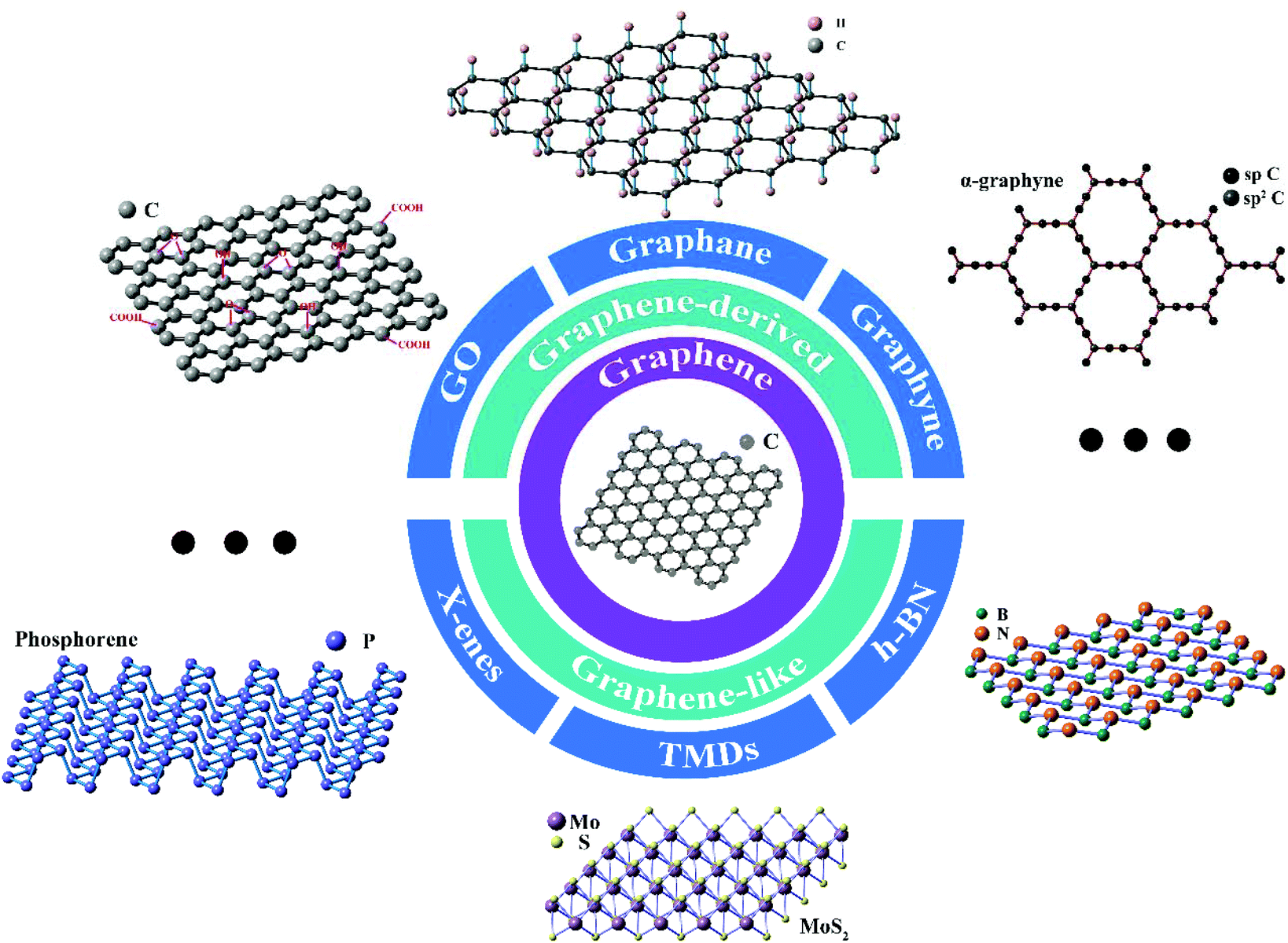 | ||
| Fig. 1 Types and structures of 2DLMs. | ||
However, the rise of 2DLMs is no doubt attributed to the excellent mechanical properties absent in their corresponding bulk materials. Since external loads are inevitable in the process of manufacture and use,48–50 2DLMs with a higher strength and flexibility will be more preferable for nanodevices. Even sometimes there is a need to design devices with specific and controllable mechanical properties by defect engineering51,52 or functionalization.53 Besides, the electronic properties of 2DLMs often vary with different external load types and load sizes,54–60 making it possible to tune the electronic properties for suitable applications. 2DLMs can also be used as ideal testbeds for fundamental studies of mechanics under extreme strains with the help of molecular dynamics (MD) and density functional theory (DFT).4,61,62 Therefore, the understanding of mechanical properties and behaviour of 2DLMs is urgently required for not only helping design nanodevices with satisfactory performance and service life, but also comprehending fundamental mechanics. On the other hand, the coupling properties between mechanical and other physical properties are not only helpful to tailor the mechanical properties of 2DLMs, but also intriguing for potential novel applications in electronics.
In this review, experimental and simulation methods exploring the mechanical properties and behaviour of 2DLMs are firstly summarized. Then, the elastic properties and failure mechanisms of 2DLMs are discussed and summarized for deeper understandings of the reasons for their unique mechanical properties and behaviour. For further tuning of the mechanical properties of 2DLMs, the factors that can greatly influence the mechanical properties and behaviour are deeply analyzed in the third part. Then, recent progresses of the coupling properties between mechanical and other physical properties (electrical, optical, thermal and structural) are covered. At last, flexible electronics based on mechanical properties and novel electronics based on coupling properties are demonstrated. The basic framework of this review is schematically shown in Fig. 2. Though some other reviews63–68 on similar topics are available, there are some apparent differences between the present review and those reviews. Castellanos-Gomez et al.63 mainly focused on the static mechanical properties of 2DLMs and the dynamics of mechanical resonators based on 2DLMs. Liu et al.64 summarized the mechanical properties of different 2DLMs and their heterostructures and discussed their applications as resonators. Papageorgiou et al.67 reviewed the mechanical properties of graphene and graphene-based nanocomposites. Androulidakis et al.68 systematically analysed the nanoindentation method and the mechanical properties of 2DLMs and heterostructures as well as their interfaces. However, it is insufficient to merely study the mechanical properties of 2DLM for their practical applications, especially in electronics where the relationship between the mechanical properties and other physical properties (e.g., electrical, optical and thermal) should be taken into consideration. Recently, Akinwande et al.65 introduced the basic progress of the thermomechanical and electromechanical properties of 2DLMs. Kim et al.66 listed some applications of the coupling properties, including strain engineering, piezoelectricity and strain sensors. The differences of the specific arrangements between this review and the two reviews in ref. 65 and 66 can be summarized as the following points. Firstly, the experimental and theoretical characterization methods are well categorized (such as the development history of various experimental methods and the main calculation formula) with their different properties from each other, which is very helpful for the readers to understand, choose and use these methods in a fast and simple way. Secondly, the elastic properties and the failure mechanisms of a wide range of 2DLMs are all deeply analyzed from the basic structures (chirality, bond types, bond strength and buckled structures) and influence factors (defects and others), offering a systematic and profound insight into their mechanical properties and behaviour. Thirdly, recent developments in both theories (electromechanical properties, optomechanical properties, themomechanical properties and strain-induced phase transition) and applications (electronics based on piezoresistive property, piezoelectric property and strain-enhanced photoabsorption) are all discussed, which will provide coherent inspiration for the readers interested in the electronics based on 2DLMs.
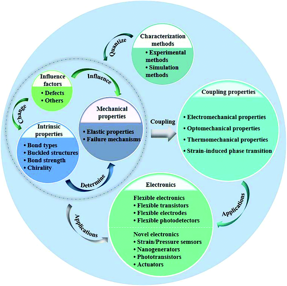 | ||
| Fig. 2 Schematic diagram of the framework of this review. | ||
2. Characterization methods
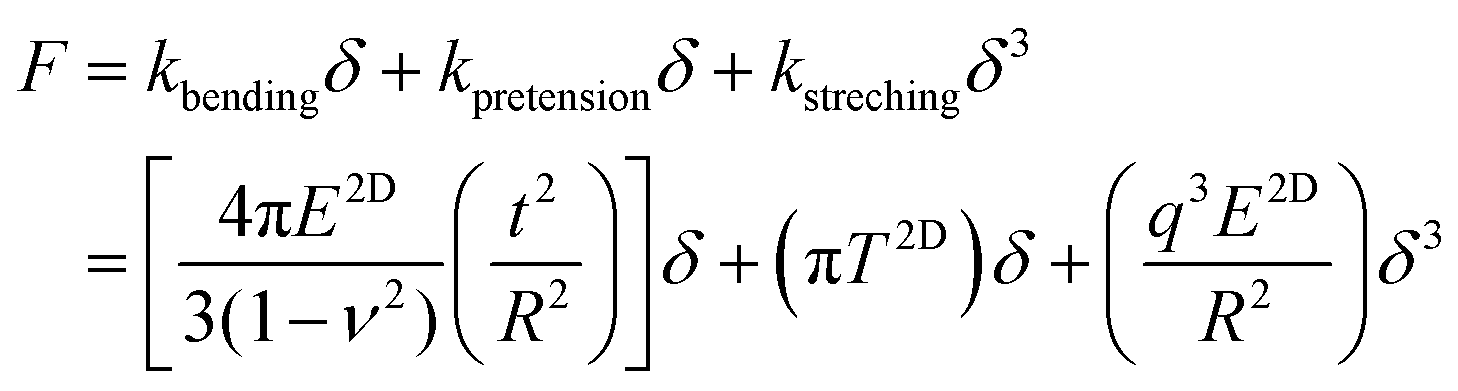
In recent years, huge efforts have been made to develop effective mechanical characterization methods based on experiments or computational simulations. Two strategies (shown in Fig. 3) have been adopted in experimental methods: indirect testing and direct testing. Indirect testing denotes that mechanical parameters can be extracted from static or dynamic deformation of 2D beams or membranes on the basis of continuum theory. Thus, the mechanical properties of 2DLMs can be extracted from the elastic stiffness. Indirect testing can be divided into resonator-based methods where the load is uniform pressure12,69 and AFM-based methods where the load is a point load.4 On the other hand, direct testing gives the opportunity for direct measurement of mechanical properties and observation of mechanical behaviour within scanning electron microscopy (SEM) or transmission electron microscopy (TEM).70–75 Besides, Raman spectroscopy can be utilized to directly map the relationship of lattice deformation and external strain in a non-destructive manner, which is very useful in the experiments of strain engineering and related applications. As for the simulation methods, though some simple and multi-scale issues can be solved by finite element model (FEM), the continuum mechanics hinder its further application at the nanoscale. Since MD and DFT have the ability of accurately simulating the mechanical behaviour during deformation from the atomic scale, these methods are effective routes for predicting the mechanical properties and investigating the nature behind mechanical behaviour. Since the strain energy density is normalized by the area of quasi 2D materials, it is more suitable to describe the mechanical properties by 2D constants (2D modulus and strength) instead of 3D constants (3D modulus and strength).4 However, 3D constants obtained by dividing 2D constants with the interlayer spacing or thickness are still indispensable for the comparison to corresponding bulk materials or other materials.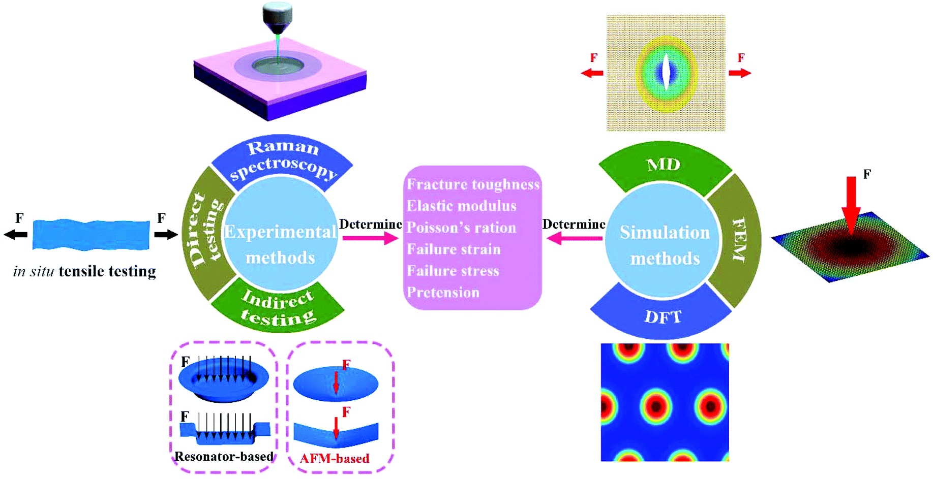 | ||
| Fig. 3 Schematic illustration of mechanical characterization methods for investigating the mechanical properties and behaviour of 2DLMs. | ||
2.1 Experimental methods
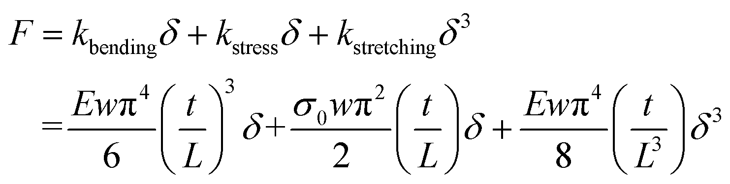
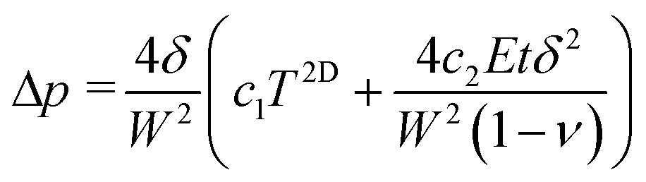
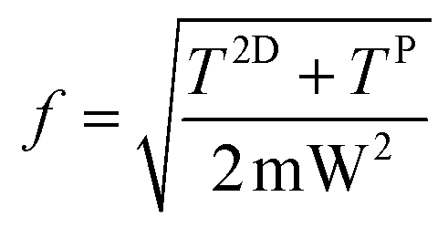
In 2007, McEuen et al.12 systematically studied the vibrations of resonators based on single- and multilayer graphene and developed the beam dynamic method. However, they76 thought it was nontrivial to determine the absolute amplitude of the motion, thus developing the beam bending method. In 2008, a pressurized blister method was further developed when they found that a monolayer graphene membrane was impermeable to standard gases.69 Meantime, Lee et al.4 established the circular membrane indentation method and found graphene was the strongest material ever measured. While in 2010, Wong et al.77 modelled the electrostatic deflection behaviour by combining analytical formulations and FEM, thus proposing the electrostatic deflection method. Based on the pressurized blister method, Lee et al.78 further developed a rapid and non-destructive method by using Raman spectroscopy. Though in situ tensile testing was originally used for measuring the mechanical properties of carbon nanotubes,79,80 it has been also reported for 2DLMs including graphene,70,71,73 h-BN,71 GO nanosheets,72,75 MoS2![[thin space (1/6-em)]](https://www.rsc.org/images/entities/char_2009.gif) 73 and MoSe274 since 2014. Very recently, Davidovikj et al.81 developed a nonlinear dynamic characterization method (or called circular membrane dynamic method) on the basis of the exact relation between the nonlinear response and the resonator's material properties.
73 and MoSe274 since 2014. Very recently, Davidovikj et al.81 developed a nonlinear dynamic characterization method (or called circular membrane dynamic method) on the basis of the exact relation between the nonlinear response and the resonator's material properties.
Even though these experimental methods have been widely used in determining the mechanical properties of 2DLMs, every method has its own advantages and disadvantages to be distinguished. In the beam dynamic method, E and T significantly depend on the effective spring constant k, and thus the measurement of resonance frequencies and amplitudes of the motions become critical. The beam bending method enables the measurements of E along arbitrary crystal orientations, which is very practical for anisotropic 2D materials.82,83 While circular membrane indentation method measures the average mechanical parameters of all orientations. Thus, this method is more suitable for isotropic 2DLMs, such as graphene,4,50 MoS284,85 and WS2.84 As for the pressurized blister method, it has only been used for the measurement of Young's modulus and pretension of graphene. Whether it could be suitable for other 2DLMs is unclear. Though no disturbances to the morphology of nanosheets will occur via a non-contact process in electrostatic deflection method, this method cannot be used to determine the breaking strength of nanosheets because of the limit of low applied pressure.86 Circular membrane dynamic method provides access to Young's modulus and pretension from high-frequency resonance measurements, allowing for the usage of very small actuation forces. The results of in situ tensile testing highly depend on the resolution and precision of nanomechanical testing device. Raman spectroscopy is mainly employed to determine the deformation of crystal lattice. Though the AFM-based methods yield stress concentration near the AFM tip, suitable for all 2D materials as well as relatively simple experiments and data processing make them more popular than the resonator-based methods. But the AFM-based methods are all operated under relative large static loading which trends to destroy 2D materials, while the resonator-based methods allow for the dynamic measurements under small driving force. In situ tensile testing is mainly used to investigate mechanical behaviour during deformation. All these experimental methods mentioned above will be discussed in chronological order of development and the summary of these methods can be obtained in Table 1.
| Loading features | Determinable mechanical properties | Method | Applicable conditions | Expressions of stiffness | Ref. | ||
|---|---|---|---|---|---|---|---|
| Bending | Pretension | Stretching | |||||
| Note: (1) denotes beam bending method; (2) denotes circular membrane indentation method; (3) denotes beam dynamic method; (4) denotes circular membrane dynamic method; (5) denotes electrostatic deflection method; (6) denotes in situ tensile testing; (7) denotes pressurized blister method. KIC is critical stress intensity factor, εm is failure strain. | |||||||
| Static point loading | E 2D, T2D | (1) | 2D beam |
|
|
|
76, 82, 83, 87 and 88 |
| E 2D, T2D, σm2D | (2) | 2D circular membrane |
|
πT2D |
|
4, 50, 85, 91–93 | |
| Dynamic uniform loading | E 2D, T2D | (3) | Conductive beam |
|
|
— | 12 and 76 |
| E 2D, T2D | (4) | Conductive circular membrane | — | 1.56πT2D |
|
81 | |
| Static uniform loading | E 2D, T2D | (5) | Conductive circular membrane | — | 4πT2D |
|
81 and 86 |
| K IC, E2D, σm2D, εm | (6) | 2D beam | — | — | — | 71–75 | |
| Static and dynamic uniform loading | E 2D, T2D | (7) | Square/circular membrane of graphene | — | 4c1T2D (square); 4πT2D (circular) |
 (square); (square);  (circular) (circular) |
69, 89 and 90 |
 | (1) |
 | (2) |
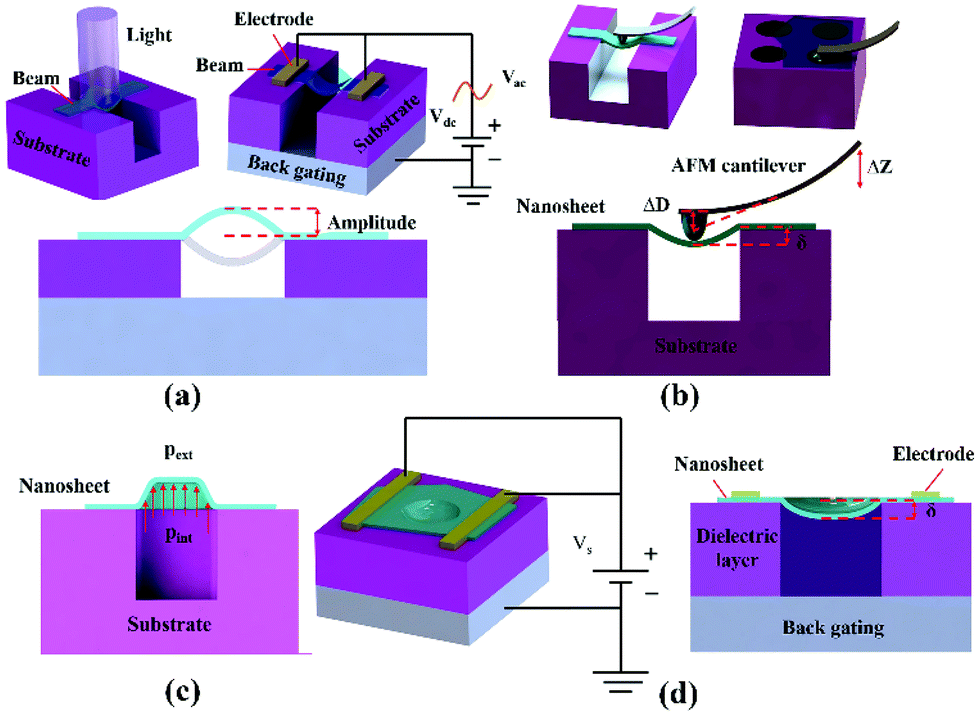 | ||
| Fig. 4 (a) Schematic of beam dynamic method. (Left inset) Light-actuated motions. (Right inset) Electric-actuated motions. (b) Schematic of AFM-based methods, including beam bending method (left inset) and circular membrane indentation method (right inset). Resulting deflection δ is determined by subtracting AFM cantilever deflection ΔD from scanning piezo displacement ΔZ. (c) Schematic of pressurized blister method. (d) Schematic of electrostatic deflection method. | ||
Apparently, beam dynamic method is a non-contact method where both E and T can be derived by a curve fit of eqn (2).
 | (3) |
Thus the Young's modulus and intrinsic stress σ0 of 2D beams can be extracted from the fits of eqn (3). Significantly, pretension T (T = σ0wt) was used instead of intrinsic stress σ0 in some studies,76,82,83,87 then the effective spring constant of beam within the linear elastic response can be used for the extraction of E and T.76,87,88
 | (4) |
 | (5) |
 | (6) |
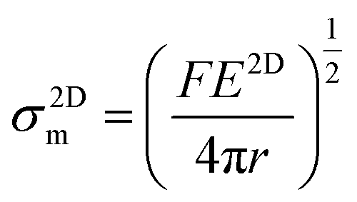
In addition to Young's modulus and pretension, breaking strength can also be derived from the model of a clamped circular membrane under a point load. Thus, the maximum stress can be derived by4
 | (7) |
 | (8) |
98 and black phosphorus.99 By combining Raman spectroscopy and numerical simulation (shown in Fig. 5(a)), the Young's modulus of graphene even has been measured.78 Since the applied strain can be accurately detected in Raman shifts, some studies100–102 have further employed Raman spectroscopy to investigate the relationship between external stain and intrinsic physical properties of 2DLMs in strain engineering.
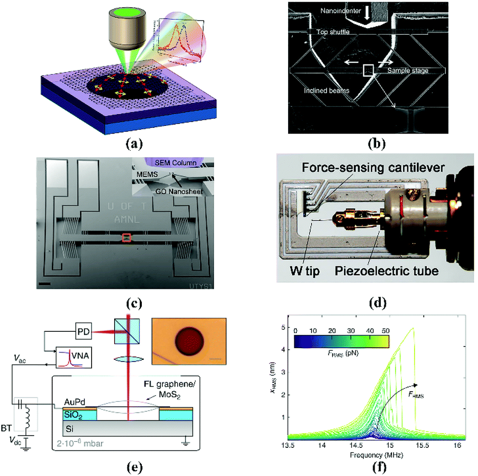 | ||
| Fig. 5 (a) Raman spectroscopy for determining the Young's modulus of pressurized graphene. (b) SEM image showing the in situ tensile testing with a nanomechanical testing device. (c) SEM image of the integrated nanomechanical testing device possessing two symmetrical thermal actuators (scale bar: 200 μm). (d) Nanomechanical testing device combining a force-measuring system and a high-precision piezoelectric tube-driven nanomanipulating system. (e) Schematic of the measurement setup. Inset: An optical image of a few-layer graphene nanodrum (scale bar: 2 μm). (f) Frequency response curves of the calibrated root-mean-square (RMS) motion amplitude for increasing electrostatic driving force. Reprinted with permission from ref. 78. Copyright 2012 American Chemical Society. Reprinted with permission from ref. 70. Copyright 2014 Springer Nature. Reprinted with permission from ref. 72. Copyright 2015 American Chemical Society. Reprinted with permission from ref. 71. Copyright 2015 American Chemical Society. Reprinted with permission from ref. 81. Copyright 2017 Springer Nature. | ||
 | (9) |
 | (10) |
2.2 Simulation methods
Simulation methods are of great importance to the study of not only determining the mechanical properties of 2DLMs, but also simulating their mechanical behaviour that cannot be realized by experimental methods above. Typically, these simulation methods can be classified as conventional modelling based on continuum mechanics (such as FEM) and atomic modelling (such as MD and DFT). Though FEM has been employed to probe the mechanical properties of 2DLMs in some studies,62,71,103–106 there is still a doubt whether continuum mechanics are suitable for atomically-thin membranes. In contrast, MD and DFT are more effective and applicable methods in this area. But it should be noted that the numbers of atoms handled in DFT is much less than that in MD. In other words, more computational costs will be necessary to investigate some complicated mechanical problems involving more atoms via the DFT calculations. On the other hand, the ability to depict energy band structure makes DFT widely adopted to study the relationship between external loading and internal band structure changes, which promotes great development of strain engineering in the 2D materials. The basic properties of these simulation methods are summarized in Table 2.| Method | Principle | Simulation size | Applicable condition | Bandgap description | Determinable parameters |
|---|---|---|---|---|---|
| FEM | Continuum mechanics | Macro scale | Simple/Multi-scale issues | no | σ, ε |
| MD | Newton's motion equations | Thousands of atoms | Complicated issues | no | E, ν, σ, ε |
| DFT | Quantum mechanics | Hundreds of atoms | Simple issues | Yes |
Usually, FEM is combined with experiments to estimate the mechanical properties of 2DLMs. During simulation, the modelling of 2DLMs in FEM based micromechanical approach is critical in guaranteeing the validity of the results. For example, atomic layer of 2DLMs is modelled as isotropic membrane under external load or pressure,105,106 but this is only applicable in some axisymmetric materials. Sometimes multiscale modelling should be considered in a more complicated system, thus a space frame modelling, where atoms and bonds are modelled as nodes and straight springs, may be more effective in accurately predicting the results.104
MD based on the integration of Newton's motion equations is an effective method for probing into the mechanical properties and behaviour of 2D nanosheets. Firstly, a simulation cell containing hundreds to tens of thousands of atoms is relaxed at a preset temperature to reach an equilibrium state through an energy minimization process. Then, loading controlled by strain rate is applied to the nanosheet along different directions. In order to obtain Young's modulus, an atomic stress method107–109 and an energy method53 are usually used in MD. Since stress–strain curve can be obtained by MD calculations, corresponding fracture stress and fracture strain are typically defined at the peak point of the curve. Additionally, the simulation process combined with stress–strain curves can give access to the mechanical behaviour of 2D nanosheets. However, it is worth noting that the accuracy of atomistic simulation highly depends on the selected models and parameters such as interaction potential, boundary conditions, cutoff distance and step time. As a consequence, a validation is necessary prior to the effective simulations.
DFT is a computational quantum mechanical modelling method that have been widely used in this area. There are similar procedures of minimization and loading as that of MD, allowing for further determination of Young's modulus (or in-plane stiffness) and Poisson's ratio by strain energy method. For homogeneous and isotropic materials, elastic constants can be derived from strain energy of the elastic deformation in the harmonic range.54,110,111 When at large strains, calculations based on nonlinear elastic theory are indispensable for describing anharmonic behaviour.62,112,113 Since some 2DLMs (WTe2,114 phosphorene,115 graphyne,116etc.) are mechanically anisotropic, a general model115 has been further developed to calculate Young's modulus along different directions.
3. Mechanical properties and behaviour
Theoretically, the mechanical properties and behaviour of 2DLMs can be understood from the variation of strain energy during their deformation as shown in Fig. 6(a). There are two regions respectively named elastic region and plastic region during deformation. In the elastic region, the strain energy monotonically increases without bonds breaking. According to the relationship between the derivative of strain energy and strain, the elastic region can be divided into harmonic region for linear relationship and anharmonic region for nonlinear relationship. Higher order terms should be considered for extracting elastic constants from the anharmonic region. When the applied strain reaches the plastic region, an irreversible structural change will occur and result in phase transitions or failure.117 The critical strain corresponding to the peak of the derivative shown in Fig. 6(a) was reported to be related to the phonon instability.111 Therefore, elastic instability and phonon instability are the two failure mechanisms of perfect 2DLMs. But some 2DLMs may exhibit ductile failure due to defects73,118,119 or interfaces.120 In this part, recent progress of both the elastic properties and failure mechanisms of different 2DLMs will be analyzed. The critical mechanical constants4,53,54,61,62,72,74,76,81–85,87,89,92,93,103,108,109,111–113,116,117,119,120,122,125,126,128,132,134,135,141,142,144–146,148,152–173 have been summarized in Fig. 14.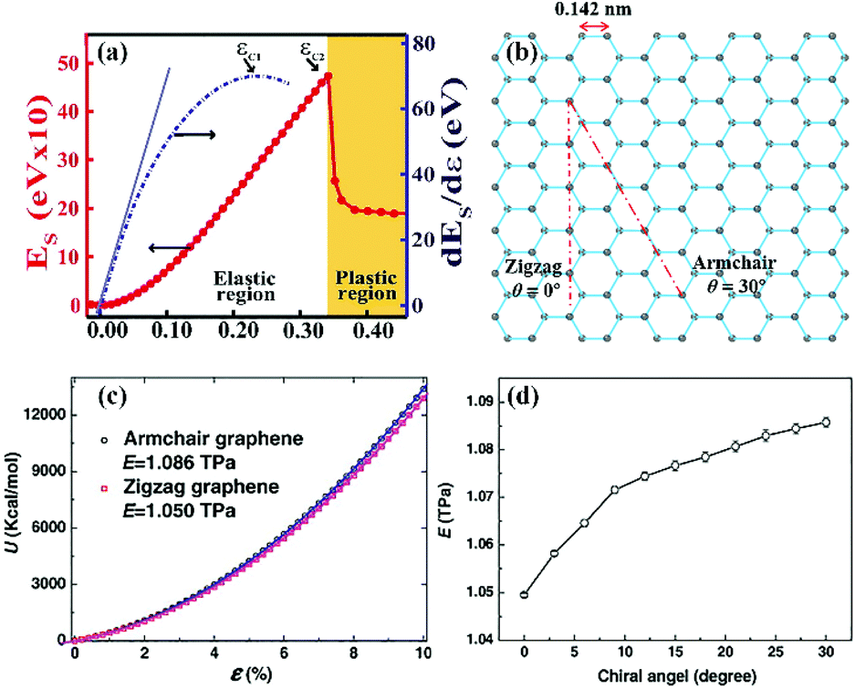 | ||
| Fig. 6 (a) The variation of strain energy ES of graphane with respect to strain ε and its derivative. (b) Chirality structure of graphene: zigzag direction for θ = 0°, and armchair direction for θ = 30°, where θ is the chiral angle. (c) U (strain energy)–ε (strain) curve of armchair and zigzag graphene sheets (GSs) (solid lines represent polynomial fitting). (d) Young's modulus of GSs for different chiral angles. Reprinted with permission from ref. 111. Copyright 2010 AIP Publishing. Reprinted with permission from ref. 53. Copyright 2010 Elsevier. | ||
3.1 Elastic properties
In 2DLMs, in-plane stiffness and Poisson's ratio play a critical role in the applications of flexible and stretchable nanodevices. Additionally, pretension is also an important parameter that should be considered in nanomechanical systems for determining deformation, resonant frequency and quality factor.103 Since in-plane stiffness and Poisson's ratio are the intrinsic properties that are highly dependent on their crystal structures, chirality, bond types, bond strength and buckled structures are very critical in determining the elastic properties of 2DLMs. Instead, pretension of 2DLMs that can only be acquired by experimental methods is susceptible to external conditions such as preparation methods, characterization methods and the environments. In order to clearly show the structural and mechanical differences of 2DLMs, these materials are classified as planar structure (graphene), sp-hybridized structures (graphyne family), buckled structures (graphane, silicene and phosphorene), honeycomb structures (h-BN, TMDs and TMCs) and heterostructures (in-plane heterostructures and out-of-plane heterostructures), and their intrinsic elastic properties will be discussed in detail.As Fig. 6(b) shows, graphene consists of in-plane hex rings where neighbour carbon atoms are separated by 0.142 nm.121 The chirality of graphene can be characterized by chiral angle θ (zigzag for θ = 0°, armchair for θ = 30°). Generally, corresponding armchair and zigzag edges can also be found in other graphene-derived and graphene-like materials. Previous AFM-based indentation experiments have demonstrated that graphene is by far the strongest material with an in-plane stiffness of 250–360 N m−1 and a pretension of 0.05–0.8 N m−1.4,122 Assuming the effective thickness is 0.335 nm, the corresponding Young's modulus is 0.75–1.07 TPa. Such a strong Young's modulus should be attributed to the extremely strong sp2 hybridization of C–C bonds and its high-quality of no defects. In addition, the elastic modulus obtained from experiments are in good agreement with that from MD108,120,123 and DFT.111 However, graphene grown by chemical methods is much weaker than pristine graphene due to the surface ripples.50 This weaker property also exists in reduced graphene oxide (rGO) monolayers whose mean Young's modulus and pretension are ∼0.25 TPa and ∼4 nN, respectively.87 Since graphene has a hexagonal structure with six-fold symmetry, its Young's modulus has been theoretically proved to be independent of the chirality as shown in Fig. 6(c) and (d). While the Poisson's ratio of graphene is around 0.16–0.17.
The structure of graphyne family (shown in Fig. 7(a)–(d)) can be formally viewed as resulting from the replacement of aromatic C–C bonds in graphene by acetylenic chains.124,125 The mechanical properties of graphyne family have been confirmed to be greatly reduced compared to graphene by simulation calculations and theoretical analysis due to the introduction of sp-hybridized acetylenic bonds.112,116,125–127 By MD simulations, the calculated 2D moduli of α- and γ-graphyne were 44 N m−1 and 174 N m−1 along zigzag direction, and 45 N m−1 and 182 N m−1 along armchair direction.116 Besides, the Poisson's ratios of γ-graphyne and graphene were much smaller than that of α-graphyne. These results were thought to be closely related to their area densities (0.1159 Å−2 for α-graphyne, 0.2902 Å−2 for γ-graphyne, and 0.3818 Å−2 for graphene), because lower area densities indicated less energy will be needed to stretch and rotate bonds. While average coordination number, in-plane atomic mass and electronic charge density were considered as the reasons for lower in-plane stiffness and higher Poisson's ratio of γ-graphyne compared to graphene through DFT calculations.112 Thus, it is not difficult to understand that the Young's modulus of the graphyne family follows a certain order: Eα < Eβ < E6,6,12 < Eγ.128 Moreover, it has been demonstrated that the in-stiffness of α-, β- and γ-graphyne decreased while the Poisson's ratio increased as the length of acetylenic chains increased (shown in Fig. 7(e) and (f)).125–127 The degradation of in-plane stiffness was a result of the reduced effective bond density, while the enhancement of Poisson's ratio was due to the weakened bending resistance of acetylenic chains.
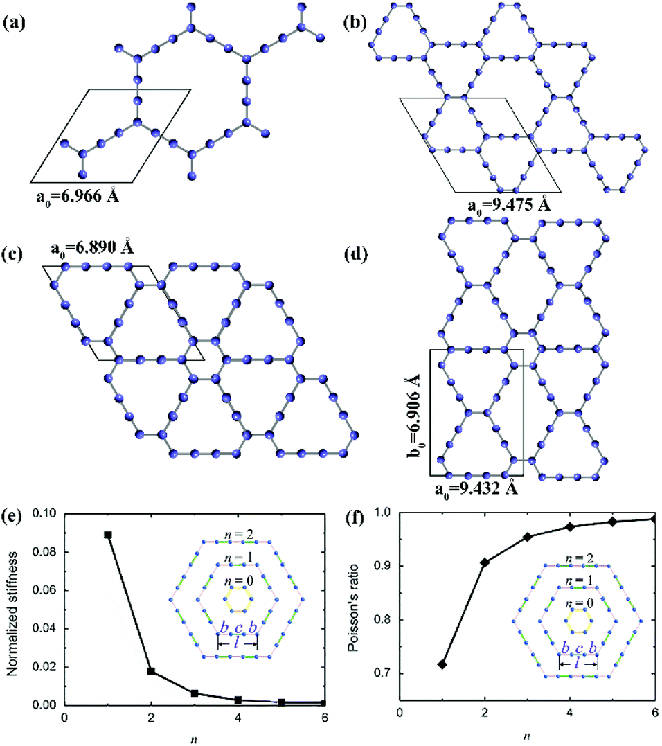 | ||
| Fig. 7 Schematic of (a) α-, (b) β-, (c) γ-, and (d) 6,6,12-graphyne. Quadrangles indicate unit cells. (e), (f) In-plane stiffness (normalized by the corresponding values for graphene) and Poisson's ratio of α-graphyne with respect to the index number n. Inset in (e) and (f) is the schematic of extended α-graphyne. Reprinted with permission from ref. 125. Copyright 2016 Springer Nature. | ||
Graphane with similar honeycomb structure has been theoretically predicted by first-principles total energy calculations129 and experimentally synthesized by exposing graphene to hydrogen plasma discharge.35 As shown in Fig. 8(a), a chair-like buckled structure in graphane is formed due to the hydrogenation of carbon atoms on both sides of the plane. According to the theoretical results, the buckling distance between the alternating carbon atoms is 0.46 Å, and the bond length of C–C and C–H are 1.52 Å and 1.11 Å, respectively.111,129 Consequently, the change of bonding type from sp2 to sp3 and the buckled structure softened the elastic properties of graphane with an in-plane stiffness of 243 N m−1.111 Besides, the Poisson's ratio of 0.07 was much smaller than that of graphene due to the reduced transverse contraction of the buckled structure.
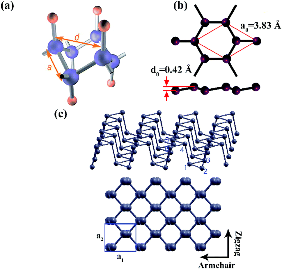 | ||
| Fig. 8 (a) Structure of buckled graphane. (b) Top (top inset) and side (bottom inset) views of buckled silicene. The lattice constant a0, buckling distance d0 and Si–Si bond length are 3.83, 0.42 and 2.25 Å, respectively. (c) Perspective (top inset) and top (bottom inset) views of buckled phosphorene. Bond lengths: d12 = d13 = 2.4244 Å, and d14 = 2.3827 Å. Bond angles: θ214 = θ314 = 97.640°, and θ213 = 98.213°. The blue box represents the basic unit cell for phosphorene with two lattice constants of a1 = 4.1319 Å and a2 = 3.6616 Å. Reprinted with permission from ref. 35. Copyright 2009 The American Association for the Advancement of science. Reprinted with permission from ref. 134. Copyright 2014 Springer Nature. | ||
Silicene is expected to have a buckled honeycomb structure (shown in Fig. 8(b)) arranged by Si atoms with an electronic dispersion resembling that of relativistic Dirac fermions.54,130 Si–Si bond is longer than C–C bond, thus the structure of silicene has to pucker to form sp3-like orbitals which can help stabilize the honeycomb structure. The results of MD131 and DFT54 calculations yielded an in-plane stiffness of 60.5–68.7 N m−1, both indicating that silicene was much less stiff than graphene because the bonding between adjacent sp3-like orbitals was much weaker than π bond in graphene. But the Poisson's ratio was found to be greater than that of graphene, which could be explained by longer Si–Si bond length and its low buckled structure.
Phosphorene has a highly puckered structure where each P atom is connected to three neighbouring P atoms as shown in Fig. 8(c). It is obvious that the armchair direction is perpendicular to the pucker and the zigzag direction is parallel to the pucker. According to the results from experiments and simulations,83,115,132 phosphorene exhibited highly chirality-dependent mechanical properties where the Young's modulus in the zigzag direction was much larger than that in the armchair direction, even reaching 3.8 times at 0 K. The reason behind was that the tensile strain in armchair direction effectively flattened the pucker rather than extensively extending the P–P bond lengths and opening the bond angles.115 When compared to other 2DLMs with similar honeycomb structures, such as graphene,4 graphane,111 WS2,84 MoS269 and h-BN,133 the weaker P–P bond strength and compromised dihedral angles made the ideal Young's modulus of phosphorene (0.166 TPa in the zigzag direction and 0.044 TPa in the armchair direction) at 0 K much smaller. Besides, the pretension of few-layer black phosphorus was determined experimentally to be in the range of 0.05–0.44 N m−1,83,93 and thicker nanosheets had smaller values because of their stronger structural stiffness. Interestingly, phosphorene has a negative Poisson's ratio of −0.027 in the out-of-plane direction when the strain is applied in the zigzag direction due to the coupling hinge mechanism where the hinge θ546 and θ214 in Fig. 8(c) are opened and closed, respectively.134 This kind of 2D auxetic material will be very desirable in the nanoscale electromechanical devices with special functions.
h-BN is a promising dielectric with a large band gap of ∼5.5 eV.133 Alternating boron and nitrogen atoms bound by strong covalent bonds arrange in a honeycomb structure as shown in Fig. 9(a). Due to the better maintained hexagonal structure and preservation of sp2-hybridized state, the theoretical Young's modulus of pristine h-BN was in the range of 716–977 GPa,135 which was very close to pristine graphene mentioned earlier. Further AFM-based indentation on 1–2 nm thick h-BN indicated that its in-plane stiffness was 220–510 N m−1.133 This may be attributed to the layer distribution of stacking faults in the CVD grown films or the error during the experimental processes. While the corresponding Poisson's ratio of h-BN (0.21–0.41136) was a little larger than that of graphene.
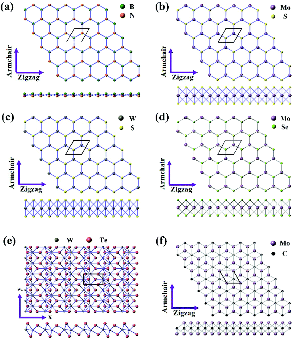 | ||
| Fig. 9 Top and side views of the atomic structure of monolayer (a) h-BN, (b) MoS2, (c) WS2, (d) MoSe2, (e) Td-WTe2, and (f) Mo2C. Black rhombus or rectangular represents a unit cell. Lattice constants: (a) a = b = 2.498 Å, c = 15 Å, α = β = 90° and γ = 120°, (b) a = b = 3.15 Å, c = 12.3 Å, α = β = 90° and γ = 120°, (c) a = b = 3.18 Å, c = 12.5 Å, α = β = 90° and γ = 120°, (d) a = b = 3.288 Å, c = 12.9 Å, α = β = 90° and γ = 120°. (e) The x direction is parallel to the W–W dimer direction, while the y direction is perpendicular to the W–W dimer direction. Lattice constants: a = 6.282 Å, b = 3.496 Å, c = 14.07 Å, α = β = γ = 90°. (f) Lattice constants: a = b = 2.994 Å, c = 4.722 Å, α = β = 90° and γ = 120°. | ||
TMDs and TMCs with similar sandwich structures consisting of three atomic layers (shown in Fig. 9(b)–(f)) have been proven to possess great potential in many practical applications.44,137–140 Previous calculations62,117,141 have demonstrated that the Young's modulus of MoS2 is about one fifth of the Young's modulus of graphene, but DFT calculations trend to underestimate the values when compared to the results from experiments.81,84,85,142 Assuming an effective monolayer thickness of 0.65 nm, the Young's moduli of single-layer and bilayer MoS2 were determined to be 270 ± 100 GPa and 200 ± 60 GPa respectively, while the pretension of single-layer MoS2 was in the range of 0.02 to 0.1 N m−1.142 Besides, the Young's modulus and pretension of MoS2 with layers of 5–25 were measured to be 0.21–0.37 TPa and 0.03–0.23 N m−1, respectively.85 Both single layer and few layers MoS2 behaved stiffer than bulk MoS2 (0.24 TPa (ref. 143)), which was attributed to the lower stacking faults in nanosheets. Due to the similar lattice constants of WS2 and MoS2, the Young's modulus and pretension of WS2 are very close to that of MoS2.84 However, the average elastic modulus (177.2 GPa (ref. 74)) of single-layer and bilayer MoSe2 measured by in situ tensile testing was a little lower than MoS2 and WS2, which may be the result of different methods of sample fabrication and characterization. Unlike isotropic 2H-MoS2, 2H-WS2 and 2H-MoSe2 discussed above, Td-WTe2 (shown in Fig. 9(c)) is a typical anisotropic 2D material whose symmetry is broken by the dimerization of the W atoms along the x direction. The direction-dependent in-plane stiffness acquired by DFT calculations144 were 4.45 eV Å−2 along x direction and 6.56 eV Å−2 along y direction respectively, while the corresponding Poisson's ratio were 0.26 and 0.38 respectively. Though there are many researches exploring the mechanical properties of TMDs, works on the mechanical properties of TMCs relatively lack. Recently, DFT calculations indicated that the Poisson's ratio of Mo2C along armchair and zigzag directions were both ∼−0.15, but the negative Poisson's ratio was valid only at strain levels below the half of the ultimate strain.144
2D heterostructures can be defined as in-plane heterostructures linked by covalent bonds in the same layer and out-of-plane heterostructures linked by weak van der Waals interaction between vertical layers. Both of them exhibit a compromised Young's modulus.84,120,145,146 Research120 on the mechanical properties of in-plane graphene-BN heterostructure revealed that Young's modulus along both armchair and zigzag directions decreased with increasing concentration of BN. Additionally, Liu et al.84 qualitatively probed into the interaction of bilayer vertical hetero- or homostructures (shown in Fig. 10(a) and (b)). Since the bottom layer was firmly clamped onto the substrate, the measured modulus of bilayer structures was mainly dependent on the contribution of the top layer which was possible to slide during the indentation tests. Further analysis indicated that interaction factor α could be employed as a parameter to compare the interlayer coupling in different bilayer hetero- or homostructures, thus determining the interaction coefficients of MoS2/MoS2, MoS2/WS2, MoS2/graphene, and graphene/graphene to be 0.75, 0.80, 0.69 and 1.0, respectively. The similar values of interaction coefficient of MoS2/MoS2 and MoS2/WS2 suggested that the interaction between MoS2 and WS2 was comparable to that in bilayer MoS2. While there was a relatively strong interaction between graphene homolayers. Besides, the mechanical properties of a kind of sandwich structure heterostructures have been theoretically studied, including graphene/MoS2/graphene145 and graphene/silicene/graphene.146 In these studies, an empirical formula has been used to predict the Young's modulus.145,146 The predicted results were 511.76 GPa for graphene/MoS2/graphene and 620 GPa for graphene/silicene/graphene, which were basically consistent with the results from MD calculations.
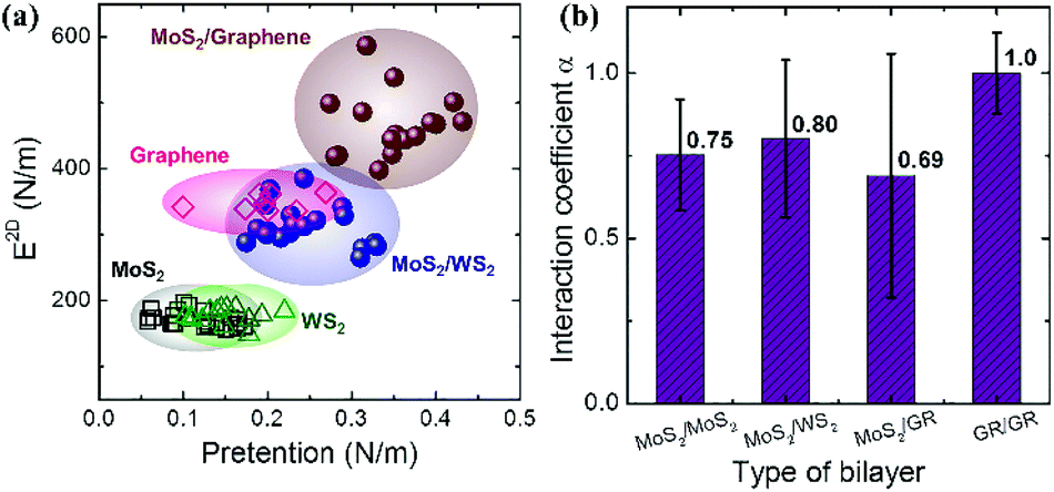 | ||
| Fig. 10 (a) Experimental data of 2D modulus and pretension for various 2D layers and heterostructures. (b) Interaction coefficients for different types of bilayers. Reprinted with permission from ref. 84. Copyright 2014 American Chemical Society. | ||
3.2 Failure mechanisms
A failure will occur when 2DLMs are strained to their limits. To avoid the failure of nanodevices based on 2DLMs, the applied stress and strain should be strictly controlled under the limit values. Herein, three failure mechanisms related to 2DLMs are discussed and summarized as shown in Table 3.| Failure mechanism | Characteristic | Conditions | Ref |
|---|---|---|---|
| Brittle failure | Failing by propagation of cracks | Materials free of defects | 71, 73 and 74 |
| Ductile failure | Plastic deformation by generation of reformed bonds or dislocations at crack-tips | Highly defected graphene | 118 and 119 |
| Highly vacancy-defected MoS2 | 73 | ||
| In-plane heterostructure graphene-BN (loading along armchair direction) | 120 | ||
| Phonon instability | Imaginary frequencies appearing before elastic instability | Graphene under equibiaxial strain | 151 |
| Graphane under uniform expansion | 111 | ||
| Silicene under uniform expansion | 54 | ||
| MoS2 subjected to biaxial strain or uniaxial strain along the armchair direction | 141 | ||
62,142 were in excellent agreement with the predicted values, further demonstrating that brittle failure may be the inherent behaviour of 2DLMs at room temperature. But the strengths of different 2DLMs exhibit huge differences because of different structures and bond strengths. With the increase of acetylenic chains introduced in γ-graphyne, 6, 6, 12-graphyne, β-graphyne and α-graphyne, their corresponding strengths were significantly reduced in turn.128 While the failure stress and strain of γ-graphyne heavily depended on the direction of the applied strain and the alignment with acetylenic chains.148 The buckled structures in graphane,111 silicene131 and phosphorene115 also lead to a greatly weakened strength compared to graphene. For vertical heterostructures, the failure is defined as the failure of any layer. Thus, their strength is expected to be limited by the layer with lower failure strain, which is the case with graphene/silicene/graphene heterostructure.146
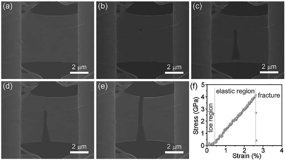 | ||
| Fig. 11 (a) SEM image of MoSe2 before tensile testing. (b)–(e) SEM images showing the fracture process. (f) Measured stress–strain curve. Reprinted with permission from ref. 74. Copyright 2016 John Wiley and Sons. | ||
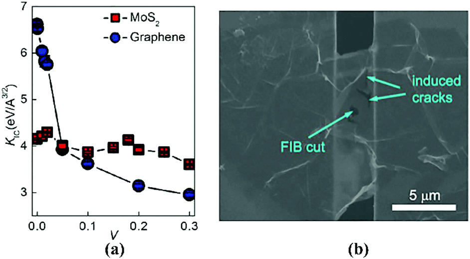
Though the intrinsic strength of these perfect 2DLMs discussed above is critical in determining the life and performance of nanodevices, it's of more practical significance to study their fracture toughness. Zhang et al.70 operated an in situ tensile testing of suspended bilayer graphene, revealing that the failure of pre-cracked graphene was due to the brittle fracture. Theoretical stress intensity factor and critical strain energy release rate were experimentally determined to be 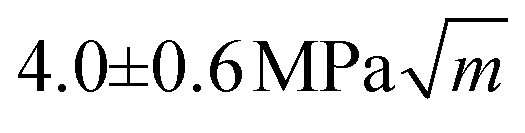 and 15.9 J m−2, respectively. While the critical stress intensity factor of multilayer graphene and h-BN was measured to be 12.0 ± 3.9 and
 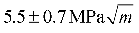 respectively by Wei et al.71 The difference between Zhang's results and Wei's results should be ascribed to the different fracture mechanisms that exist in bilayer graphene and multilayer graphene. Bilayer graphene fractured along a smooth edge while multilayer graphene and h-BN exhibited rough fracture edges caused by crack meandering and branching which could increase the energy required for a crack to propagate. Recently, MD calculations149 revealed that the failure stress and strain for armchair and zigzag directions trended to decrease with the increase of pre-crack size in graphene. The critical stress intensity factors of pre-cracked graphene at 0 K and 300 K were calculated to be
 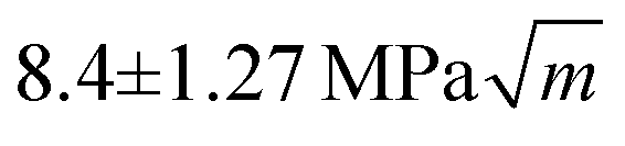 and
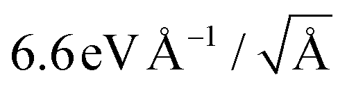
and  , respectively. However, the fracture toughness of graphene obtained above is relatively low compared to conventional bulk materials,75 which will induce reliability issues in their further applications as nanodevices. To improve the fracture toughness of graphene, high fracture toughness of ∼39 J m−2 was realized by chemical functionalization.75 MD simulations indicated that the interactions among functionalized atoms in constituent layers and distinct fracture pathways in individual layer resulted in the huge enhancement of fracture toughness. As for TMDs, it was found that the crack propagation of CVD-grown monolayer MoS2 preferentially occurred along the zigzag direction during brittle fracture,73 differing from graphene for fracturing along both armchair and zigzag directions.150 With the increase of vacancy density, a gentle reduction of fracture toughness of MoS2 was observed while graphene has a more dramatic change in fracture toughness (shown in Fig. 12(a)). Though Yang et al.74 have attempted to measure the fracture toughness of MoSe2, catastrophic fracture (shown in Fig. 12(b)) is unavoidable during the introduction of pre-crack by focus ion beam (FIB). Therefore, how to fabricate the samples of 2DLMs with great brittleness for fracture toughness measurement is a big challenge for future exploration of their mechanical properties. The fracture toughness mentioned above is summarized in Table 4.
 | ||
| Fig. 12 (a) Comparison of fracture toughness as a function of vacancy density for MoS2 and graphene. (b) Catastrophic fracture of MoSe2 during FIB cutting. Reprinted with permission from ref. 73. Copyright 2016 American Chemical Society. Reprinted with permission from ref. 74. Copyright 2016 John Wiley and Sons. | ||
| Materials | Synthetic method | Layers | Fracture toughness | Ref. | |
|---|---|---|---|---|---|
|
|
G C (J m−2) | ||||
| Graphene | — | 1 |
|
2.3 eV Å−1 | 73 |
| Graphene | CVD | 2 | 4.0 ± 0.6 | 15.9 | 70 |
| Graphene | Arc-discharge | 6–20 | 12.0 ± 3.9 | — | 71 |
| h-BN | Induction heating | 10–12 | 5.5 ± 0.7 | — | 71 |
| MoS2 | CVD | 1 |
|
2.5 eV Å−1 | 73 |
| GO | Chemical functionalization | ∼21 | — | 34–39 | 75 |
| GO | Chemical functionalization | ∼30 | — | 81 | 75 |
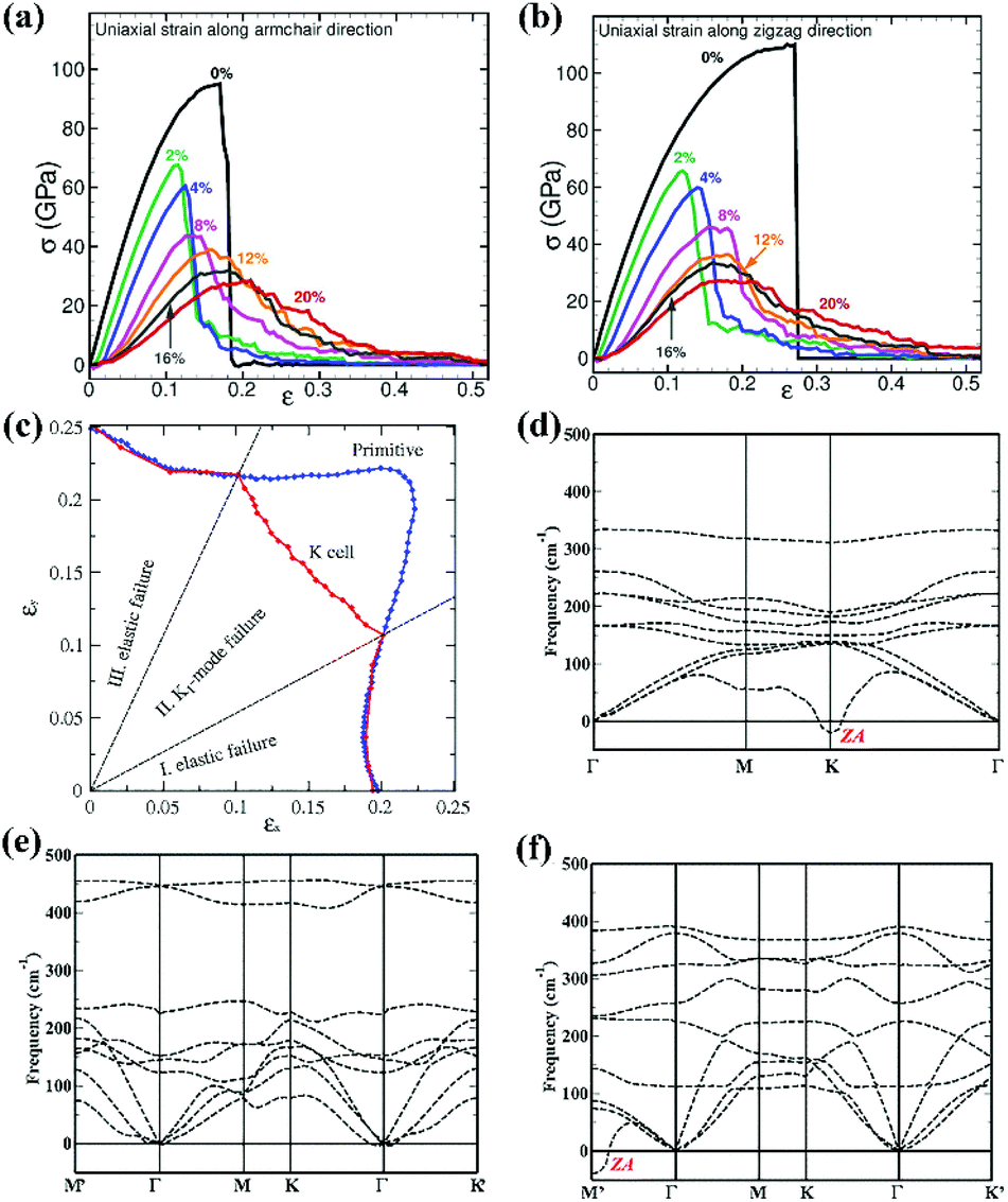 | ||
| Fig. 13 Stress–strain response of defective single-layer graphene (vacancy concentrations are indicated in the figure) subjected to uniaxial tensile strain along armchair (a) and zigzag (b) directions. (c) The maximum stable strain for the primitive unit cell (blue curve) and the K cell (red curve) as a function of all possible linear combinations of zigzag and armchair uniaxial tensile strains. Calculated phonon dispersion for single layer MoS2 at (d) biaxial tension with ε = 0.195, (e) uniaxial tension along zigzag direction with ε = 0.36 and (f) uniaxial tension along armchair direction with ε = 0.28. Reprinted with permission from ref. 119. Copyright 2013 AIP Publishing. Reprinted with permission from ref. 151. Copyright 2010 American Physical Society. Reprinted with permission from ref. 141. Copyright 2012 American Physical Society. | ||
Even though previous phonon calculations have demonstrated that elastic instability is the failure mechanism of graphene under uniaxial strain in armchair and zigzag directions,152 further summarizations151 of all possible failure mechanisms of pure graphene at 0 K (shown in Fig. 13(c)) indicated that the strength of graphene was limited by the phonon instability under equibiaxial strain. However, the calculated failure strain of 0.151 caused by the K1 mode was much smaller than the experimental results of 0.225,4 which may be attributed to the differences in temperature and the reaction between tip and graphene. Phonon instability has also been proven to be the failure mechanism in graphane and silicene under uniform expansion, yielding a failure strain of ∼0.23111 and ∼0.18,54 respectively. Besides, DFT calculations have found that the tensile strength was dictated by phonon instability when MoS2 was subjected to biaxial strain (shown in Fig. 13(d)) or uniaxial strain along the armchair direction (shown in Fig. 13(e)), while limited by elastic instability for the zigzag direction (shown in Fig. 13(f)).141 The predicted ideal strengths are in great agreement with the experimental results,85,142 further verifying the validity of the calculation results. But this phonon instability present in MoS2 is due to the out-of-plane atomic relaxation upon in-plane strain which is different from that of the truly 2D graphene.
4. Influence factors on the mechanical properties
During the process of growth, transfer, design, fabrication and usage, the factors of great influence on intrinsic mechanical properties of perfect 2DLMs should be taken into consideration for practical applications. In turn, the mechanisms of these factors provide effective means for accurately tailoring their mechanical properties.4.1 Defects
Noted that the difference of mechanical properties of 2DLMs fabricated by different methods could be attributed to the influence of produced defects, and thus it is possible to tailor the mechanical properties during their fabrications.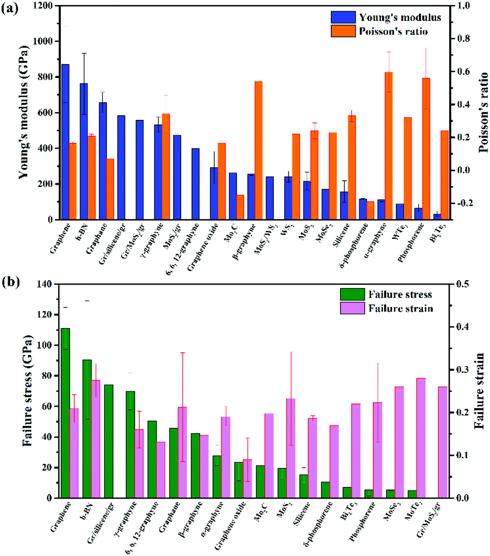 | ||
| Fig. 14 (a) Young's modulus and Poisson's ratio with standard deviations of 2DLMs. (b) Failure stress and strain with standard deviations of 2DLMs. | ||
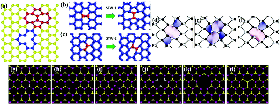 | ||
| Fig. 15 Point defects in 2DLMs. (a)–(c) Vacancy and SW defects in graphene. Red C–C bond rotates by 90° to the SW-1 defect (b) and red C–C bond rotates by 90° to the SW-2 defect (c). (d)–(f) Vacancy and SW defects in phosphorene, including divacancy (d), SW (e) and monovacancy (f). (g)–(l) Six types of point defects in MoS2 observed in experiments. From left to right: monosulfur vacancy (g), disulfur vacancy (h), antisite defects where a Mo atom substituting a S2 column (i), vacancy complex of Mo and nearby three sulfur (j), vacancy complex of Mo nearby three disulfur pairs (k) and antisite defects where a S2 column substituting a Mo atom (l). Reprinted with permission from ref. 123. Copyright 2011 AIP Publishing. Reprinted with permission from ref. 174. Copyright 2014 Elsevier. Reprinted with permission from ref. 175. Copyright 2014 American Chemical Society. Reprinted with permission from ref. 176. Copyright 2013 American Chemical Society. | ||
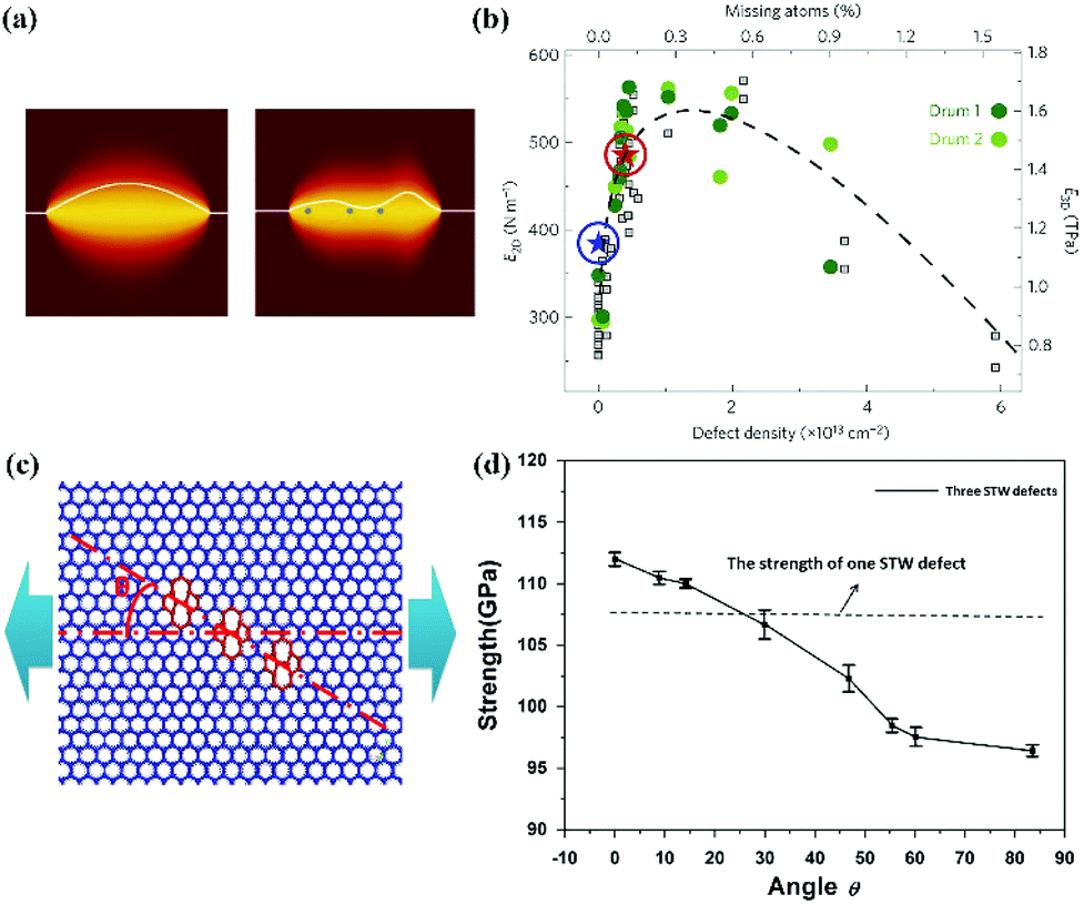 | ||
| Fig. 16 (a, b) Experimentally determined 2D Young's modulus (E2D) of graphene with various defect densities. Left picture in (a) depicts the thermal fluctuation of a suspended graphene membrane, while right picture indicates that long-wavelength fluctuations are quenched in the presence of defects. (c, d) Strength of defective graphene with SW defects. The strength represented by the dashed line in (d) is 107.60 GPa, corresponding to the strength of graphene with a single SW-1 defect stretched along the zigzag direction. Reprinted with permission from ref. 122. Copyright 2014 Springer Nature. Reprinted with permission from ref. 174. Copyright 2014 Elsevier. | ||
Meanwhile, the mechanical behaviour of 2DLMs can also be influenced by vacancies and SW defects. The failure behaviour of highly defective graphene with vacancies and SW defects can be transformed from brittle rupture to ductile fracture due to the combined results of crack trapping, crack-tip blunting and crystalline-to-amorphous transition.118,119 In addition, in situ observation of the fracture of monolayer MoS2 with high S vacancies confirmed that the line defects formed by the aggregation of S vacancies could help to guide and deflect the crack in propagation, thus inducing the brittle-to-ductile transformation.73 Besides, by MD simulations, the nucleation and evolution of a fracture induced by vacancies and SW defects in h-BN were even directional.167
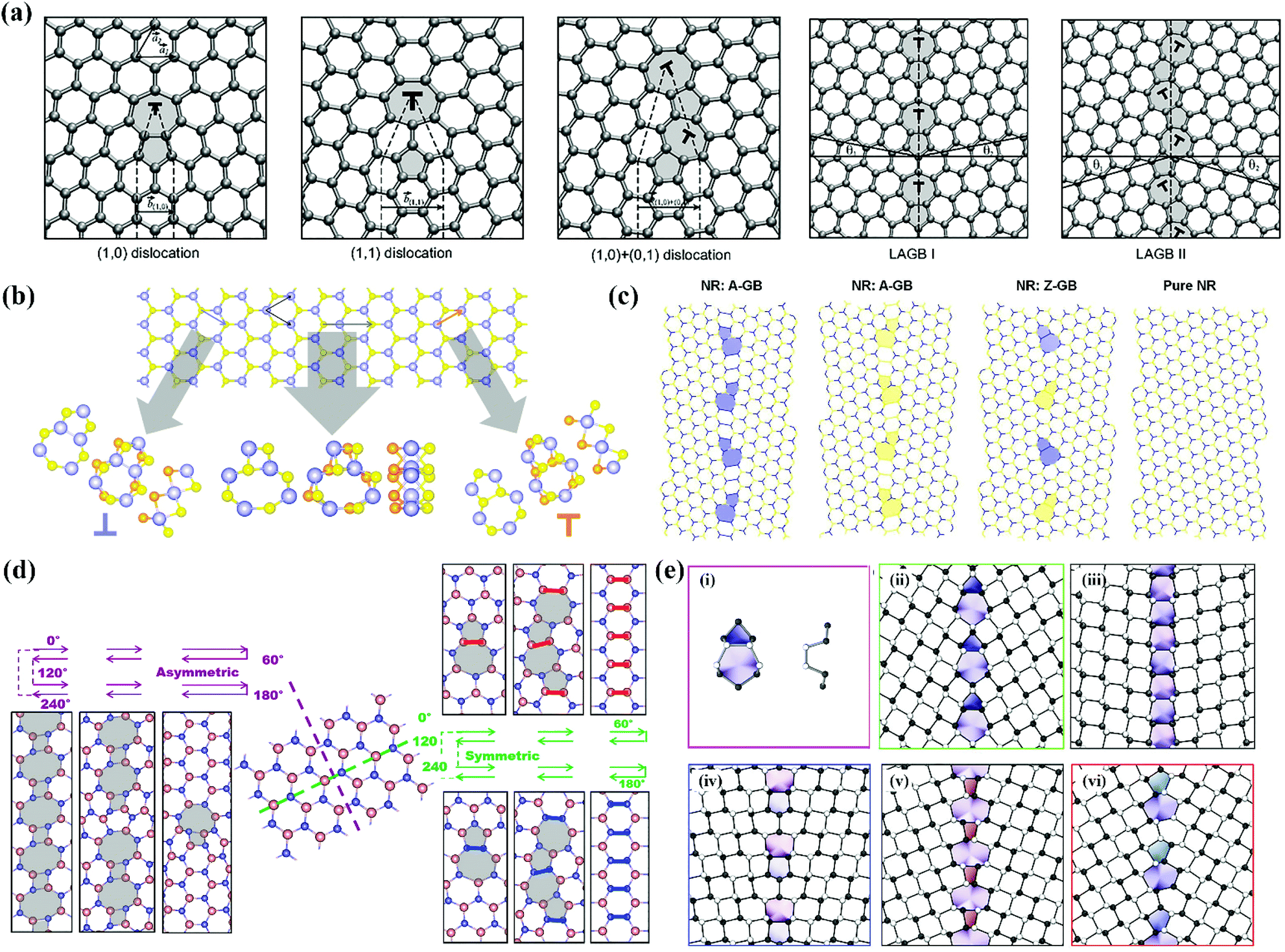 | ||
| Fig. 17 (a) Atomic structures of (1, 0), (1, 1) and (1,0) + (0,1) dislocations as well as the θ = 21.8° (LAGB I) and the θ = 32.2° (LAGB II) symmetric large-angle grain boundaries in graphene. (b) Basic edge dislocations formed by removal of shaded atoms from the MS2 (M = Mo or W) lattice. Each atomic structure is shown in front, isometric, and side (along the layer) views, with atoms colored blue (metal, M), yellow (front/top layer sulfur, S) and orange (back/bottom layer sulfur, S′). (c) Atomic structures of grain boundaries for mirror-symmetric armchair A-GB and asymmetric zigzag Z-GB in MS2 (M = Mo or W). (d) Ground state structures of grain boundaries as a function of tilt angle in h-BN. (e) Top and side view (i) of the core structure of the primary dislocation with a Burgers vector (0, 1) and structure of grain boundaries at various misorientation angles in phosphorene (26.8° for (ii), 71.1° for (iii), 110° for (iv), 130° for (v) and 149° for (vi)). Reprinted with permission from ref. 177. Copyright 2010 American Physical Society. Reprinted with permission from ref. 178. Copyright 2013 American Chemical Society. Reprinted with permission from ref. 179. Copyright 2012 American Chemical Society. Reprinted with permission from ref. 175. Copyright 2014 American Chemical Society. | ||
It is natural to believe that grain boundaries can reduce the mechanical properties of 2DLMs according to continuum mechanics theory. This weakening effect has been confirmed in graphene180,181 and MoS2.182 But this point is proved to be unreliable to a certain extent by simulations107 and experiments.155 By MD and DFT calculations, it was suggested that the failure stress and strain would increase when the grain boundary angle increased.107 This was ascribed to the fact that graphene with higher grain boundary angle had a bond length closer to that of the pristine graphene. However, the upper bound of in-plane breaking stress of graphene determined by AFM indentations50 was lower than the theoretically predicted values,107 which could be understood by the combined weakening effects of voids near boundary and the shear of boundaries under indentations. While in another study, the difference between the theoretical predictions and AFM indentation values was attributed to the fabrication methods of samples.155 As a result, a new method for sample fabrication was developed by using ammonium persulfate for copper etching and polydimethylsiloxane for dry transfer. It was interesting to note that the grain boundary angle had no obvious effect on the strength of graphene in this study. This arose from the energy-minimizing structure of random asymmetric grain boundaries that could result in a smaller misfit “prestrain” of the critical bonds in boundaries. On the other hand, it was indicated that the combination of the defect densities and the detailed arrangements of grain boundaries deeply affected the mechanical properties since the strength of grain boundaries could either increase for evenly spaced pentagon–heptagon defects or decrease for other cases.180
For graphene, functionalization can be considered as the introduction of sp3 bonds, thus resulting in the rise of carbon atoms with functional groups from the original plane. By MD and MM simulations,53 the Young's modulus of graphene was reported to decrease linearly with the increasing coverage of hydroxyl groups because off-plane sp3 bond was much easier to be bent and broke the local bond. Besides, functional group with higher binding energy had a more adverse effect on the Young's modulus, accounting for the reduction degree of graphene with carboxyl groups was bigger than that of graphene with propyl and methyl hydroperoxide groups. On the contrary, molecular weights of functional groups may have no obvious effect on the Young's modulus of graphene. The failure stress and strain trend to have a stronger sensitivity to functionalization than Young's modulus.108,109 For example, functionalization of even one H atom in graphene can lead to a relative different drop in Young's modulus, failure stress and strain by 0.1%, 13% and 30%, respectively.108 This can be understood from two aspects: (1) Young's modulus is a measure of average deformation of the whole system in the small strain regime while failure stress and strain are limited by the breakage of the weakest bonds; (2) sp3 hybridized bonds are weaker than sp2 hybridized bonds and will result in local stress concentration. Moreover, the location and distribution of introduced groups could also influence the strength of graphene.109 Results showed that surface functionalization had a stronger effect than edge functionalization because edge functionalization only terminated the dangling bonds of graphene edges without the formation of sp3 bonds. For different distributions, methyl groups arranged in line perpendicular to the tension direction led to a greater drop of failure stress and strain than that parallel to the tension direction. If the sp3 bonds are viewed as weaker phase in graphene, it is not difficult to understand that the strong sp2 bond network will be destroyed to the largest extent when the sp3 bonds are arranged in line perpendicular to the tension direction. Even though the introduction of sp3 bonds will degrade the mechanical properties of graphene, a relative small number of sp3 bonds between bilayer graphene can achieve optimal load transfer rate and stability.156
Graphene oxides (GO) (shown in Fig. 18(a)) can be considered as graphene functionalized by oxygen-containing groups, such as hydroxyl (–OH) and epoxy (–O–) groups on the basal plane and carboxyl groups on the edge.34,187 The functionalization of oxygen-containing groups breaking the sp2 bond network is the reason for the weaker mechanical properties103,160,161 than graphene. DFT calculations of the Young's modulus and strength of single-layer GO revealed that the increasing coverage of groups could further weaken its mechanical properties because of the breakage of sp2 bond network.161 But OH/O ratio had little effect on the mechanical properties of GO when the coverage maintained constant, indicating the coverage instead of the types of functional groups was the main factor in reducing the mechanical properties of GO. The weakening effect of coverage was further confirmed by AFM indentations where the obtained Young's moduli of monolayer GO with ∼20% functionalization and ∼40% functionalization were 269 ± 21 N m−1 (ref. 160) and 145.3 ± 16.4 N m−1,103 respectively. Besides, the active oxygen-containing groups attached on GO makes it possible to synthesize composite materials with enhanced mechanical properties.34 Due to different fracture mechanisms among monolayer GO, GO nanosheets and GO papers, the failure behaviour transforms from interlayer fracture for GO papers (or bulk GO) to absolute intraplanar fracture for monolayer GO,72 accounting for the orders of magnitude discrepancy in strength (24.7 GPa for monolayer GO,160 12 GPa for GO nanosheets72 and ∼100 MPa for GO papers34,188).
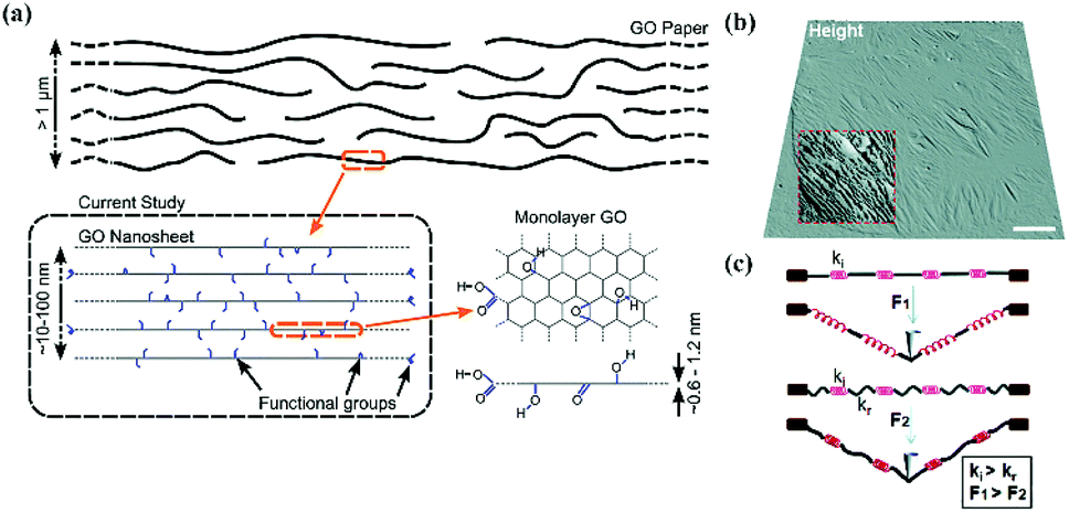 | ||
| Fig. 18 (a) Schematic of the hierarchical units forming the basis of GO materials. (b) AFM height tapping mode image of graphene. The region in the red box is enlarged in the z direction. (c) Model illustrating a flat and a rippled graphene cross section. The springs have a spring constant ki representing graphene's intrinsic elastic modulus. While flattening ripples have a much smaller spring constant kr. Reprinted with permission from ref. 72. Copyright 2015 American Chemical Society. Reprinted with permission from ref. 50. Copyright 2011 American Chemical Society. | ||
189 and h-BN.190 The softening effect of these ripples could be understood from the models of a rippled membrane and a flat membrane with negligible bending stiffness as shown in Fig. 18(b). Thus, less force will be required to flatten the rippled membrane than to stretch the flat membrane, perfectly accounting for the softened Young's modulus of CVD grown graphene with sizable ripples.50
4.2 Others
Other researches have demonstrated that strain rate and substrate roughness have great influence on the mechanical properties and behaviour. While for material like phosphorene with chemical instability in the atmosphere, the exposure in the atmosphere will further reduce its mechanical properties.5. Coupling properties
5.1 Electromechanical properties
With the increasing applications of 2DLMs for electronic devices, the influence of electromechanical coupling behaviour on device performance becomes more and more prominent. Not only external electric fields show great influence on mechanical properties of 2DLMs, but also the intrinsic electrical properties of 2DLMs can be tailored by external strain or pressure.Actually, when a thin nanostructure is exposed to an external electric field, a moment of force arising from the electric polarization effect will be generated and further evoke the nanostructure's deformation as shown in Fig. 19.199,200 Besides, it has been experimentally observed that the field-induced ripples of graphene can be enhanced by the increase of the transverse electric field.201 The novel electro-mechanical coupling behaviour stimulates the systematic studies of the effect of electric field on the mechanical properties of 2DLMs. MD calculations revealed that the Young's modulus and fracture stress of graphene under uniaxial tension decreased with the rise of vertical electric potential and net charges.202 Fracture always originated at the edge of graphene because the increased bond length at the edge of graphene made the edge weaker than the center, which was very different from the case of no fields and charges.203 Recently, AFM indentation experiments demonstrated that the Young's modulus and fracture strength of suspended graphene with various thicknesses would remain approximately constant until the normalized electric field strength of 0.18 ± 0.03 V nm−1 was reached.204Fig. 19(e)–(j) show the fracture processes of graphene under different electric field strengths. The excessively regional Joule heating may be the main reason for the fracture of graphene.
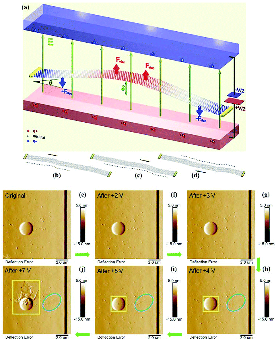 | ||
| Fig. 19 (a) Topographic diagram of charge distribution on a suspended graphene nanoribbon (GNR) in a transverse electric field E from molecular simulations. (b–d) Representative atomic configurations of the graphene at room temperature from MD simulations before the field is applied. (e)–(j) Deflection error maps of graphene nanosheet before and after the conductive AFM nanoindentation process with increasing bias voltages. Reprinted with permission from ref. 199. Copyright 2010 American Physical Society. Reprinted with permission from ref. 204. Copyright 2017 American Chemical Society. | ||
Since the electronic properties mainly depend on the band structure, most studies focus on the variation of band structures of 2DLMs during the deformation. Though the carrier mobility of semimetal graphene is ultrahigh,49 graphene seemed to be less sensitive to applied strains,56 resulting in that the opened bandgap was too small to significantly promote its applications in semiconductor devices. On the contrary, a wide range of 2DLMs have been reported to possess a tunable electronic and optoelectronic properties with the variation of external strain and show a sizable sensitivity to the applied strain.54–60,110,111,114,141,161,205–207 DFT calculations revealed that the unstrained TMDs (MX2; M = Mo, W and X = S, Se, Te) possessed semiconducting bandgaps of 1.06–1.81 eV.56 All these TMDs were very sensitive to the external strains as shown in Fig. 20(a), resulting in the transition of direct-to-indirect band gap and semiconductor-to-metal. The reduction in bandgaps of TMDs was further confirmed by the very recent experiments.59 Under a three-dimensional pressure, a pressure-induced semiconducting to metallic transition in multilayered MoS2 was observed at ∼19 GPa owing to the enhanced sulphur–sulphur interactions as the interlayer spacing reduced (shown in Fig. 20(b) and (c)).208 However, in contrast to the decrease in the bandgaps of TMDs with the increasing strain, the bandgap of γ-graphdiyne kept increasing from 0.28 to 0.71 eV with the character of direct bandgap within the uniform strain ranging from −0.05 to 0.06.110 Even more complicated variation of bandgaps instead of monotonous changes with external strains have been found in other 2DLMs,58,111 suggesting that the mechanisms behind vary with the structures of studied materials. While for highly anisotropic materials, the variation of band structures and electronic properties with external strains are also highly anisotropic, such as phosphorene,57 TiS360 and Td-WTe2.114
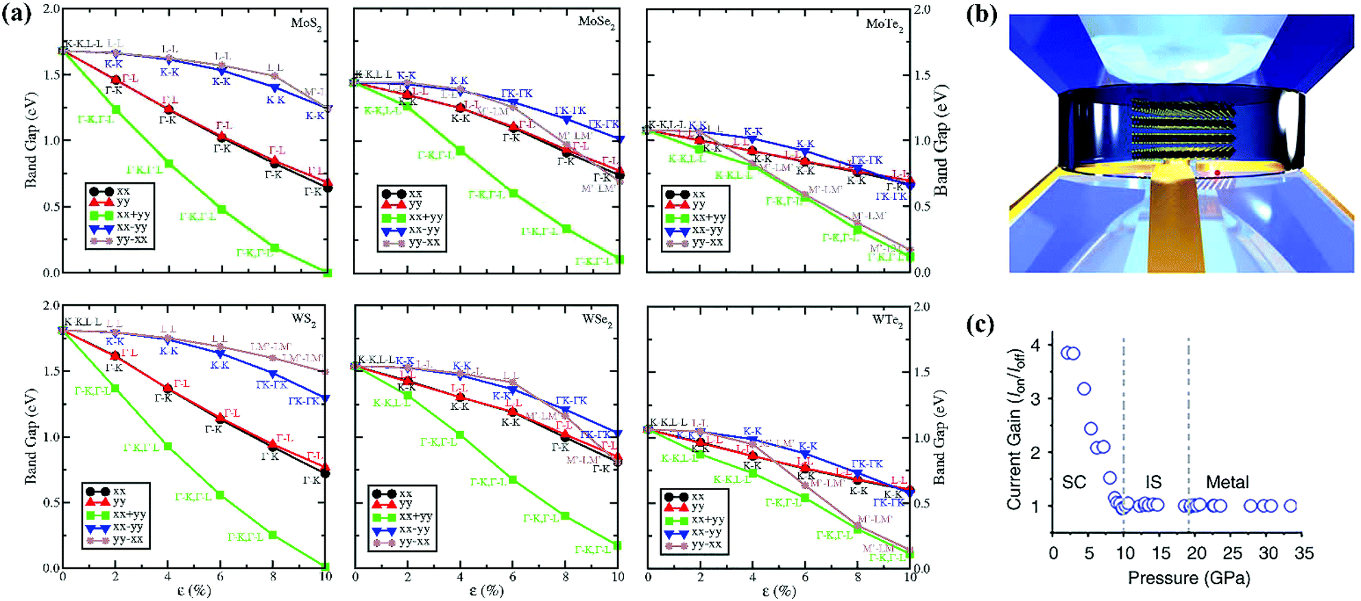 | ||
| Fig. 20 (a) Band gap of monolayer TMDs with respect to strain, ε. (b) A 3D illustration of multilayered MoS2 in a high-pressure diamond anvil cell (DAC) for compression experiments. (c) Current gain (defined as Ion/Ioff ratio) as a function of pressure when exposed to a 532 nm (2.3 eV) laser light with an intensity of 40 W m−2. Reprinted with permission from ref. 56. Copyright 2012 American Chemical Society. Reprinted with permission from ref. 208. Copyright 2014 Springer Nature. | ||
Except for the band structure, the modulation of the magnetic properties tightly related to lattice structure can also be realized by local strain. By combining experiments with calculations, strain-induced magnetization was confirmed on wrinkle of ReS2 due to the spin polarization.102 Besides, the tensile strain can also alter the redistribution of spin-polarized electrons induced by lattice distortion.209 It was revealed that the local magnetic moments and ferromagnetic stability in graphene with topological line defect were enhanced under tensile strain along the zigzag direction, while diminished under tensile strain along the armchair direction. Moreover, half-fluorinated BN and GaN exhibited intriguing magnetic transitions between ferromagnetism and antiferromagnetism by strain regulation due to the combined effects of both through-bond and p–p direct interactions.210 DFT calculations disclosed that pristine VX2 (X = S, Se) monolayers exhibited a variable exciting ferromagnetic behaviour tuned by isotropic strains, which could be utilized for the design of mechanical switch for spin-polarized transport.211
The piezoresistive effect of 2DLMs is an important property that pave the way to nano-scale piezoresistive sensors with high sensitivity. Basically, the piezoresistive behaviour is believed to be a superposition of carrier density and carrier mobility modification.212 Experiments and simulations on graphene showed that its piezoresistive property depended on whether it was strained uniaxially or biaxially, but was independent of crystallographic orientation and doping concentration.212,213 Interestingly, the experiments on CVD-grown graphene even reported a strain-dependent resistance where the conductance slightly increased, dramatically decreased and suddenly dropped with the gradual increase of uniaxial strain. This unique behaviour should be attributed to three stages of the relaxation of pre-existing winkles, the elastic deformation and the plastic deformation, respectively.214 In contrast to graphene, MoS2 exhibited a negative piezoresistive behaviour, indicating its decreasing resistance with the increasing strain.215 Furthermore, the piezoresistive property of MoS2 was suggested to be highly related to the layer number. The studies on black phosphorus indicated the gate doping could also induce huge influence on the piezoresistive response owing to the modulated bandgap.216 While for highly-anisotropic material like ReS2, the strain induced broadening and narrowing of the bandgap along two principle directions, resulting in completely opposite piezoresistances (positive and negative).217
Piezoelectric effect is of great importance in the applications of sensors218 and power generation.219 Specially, when materials with polarization domains or non-centrosymmetric structures are strained along a certain direction, internal polarization will induce heterogeneous charges on opposite surfaces. Due to the absence of an inversion center, single-layer h-BN, group VI TMDs (MX2, M = Mo, W, Cr and X = S, Se), group IV monochalcogenides (MX, M = Sn, Ge and X = S, Se) are theoretically proposed to exhibit piezoelectricity.220–224 Though intrinsic graphene was believed to be devoid of piezoelectricity, DFT calculations predicted that doping graphene on one side was a feasible route for gaining piezoelectricity.225 Experimentally, in-plane piezoelectric effect and out-of-plane piezoelectric effect were obtained in strained/unstrained graphene junction226 and supported graphene on SiO2,227 respectively. It was worth noting that the first experimental observation of piezoelectricity in 2DLMs was in single-layer MoS2228 rather than graphene. With the presence of piezoelectric charge, the current–voltage curve of single-layer MoS2 device shifted leftwards or rightwards under tensile strain or compressive strain, respectively. The detectable piezoelectric effect could only be observed in MoS2 with an odd number of layers, because flakes with even atomic layers were centrosymmetric owing to the opposite orientation of alternating layers. Further studies229,230 confirmed this piezoelectric response in monolayer MoS2, and the piezoelectric polarization was reported to highly depend on its crystal orientation.230 Similarly, strong piezoresponse was found in WSe2 odd-layers via laterally excited scanning probe microscopy.231 Though the piezoelectric behaviour in WSe2 even-layers was negligible,231 it was interesting that reliable piezoelectric property was obtained from WSe2 bilayers fabricated by turbostratic stacking.232
Since the piezoresistive and piezoelectric effects are critical in tailoring the electromechanical properties of 2DLMs towards applications in electronics, the results of recent simulation and experiments on the piezoresistive and piezoelectric properties are summarized as shown in Table 5.
| Material | Fabrication method | Gauge factor | Strain type | Method | Ref. |
|---|---|---|---|---|---|
| Piezoresistive properties | |||||
| Graphene | — | 2.2 | Uniaxial | Simulation | 212 |
| Graphene | — | 1.25 | Biaxial | Simulation | 212 |
| Graphene | CVD | 3.91 | Uniaxial | Experiment | 212 |
| Graphene | CVD | 6.73 | Biaxial | Experiment | 212 |
| Graphene | CVD | 2.92 | Pressure | Experiment and simulation | 213 |
| MoS2 | — | −43.5 to −224 | Uniaxial | Simulation | 215 |
| Black phosphorus | — | 185 | Uniaxial | Experiment | 216 |
| ReS2 | Mechanical isolation | 50.14 | A-Axis | Experiment and simulation | 217 |
| ReS2 | Mechanical isolation | −60.49 | B-Axis | Experiment and simulation | 217 |
| Material | Fabrication method | Piezoelectric coefficient | Strain type | Method | Ref. | |
|---|---|---|---|---|---|---|
| e 11 (10−10 C m−1) | d 11 (pm V−1) | |||||
| Piezoelectric properties | ||||||
| Strained/unstrained graphene junction | Mechanical isolation | — | 37000 |
Biaxial | Experiment | 226 |
| Graphene on SiO2 calibration grafting substrates | CVD | — | 1400 | — | Experiment | 227 |
| h-BN | — | −1.19 | — | — | Simulation | 220 |
| h-BN | — | 1.38 | 0.60 | Uniaxial | Simulation | 221 |
| MoS2 | — | 3.64 | 3.73 | Uniaxial | Simulation | 221 |
| MoS2 | — | 3.62 | 3.65 | Uniaxial | Simulation | 224 |
| MoS2 | Mechanical isolation | 2.9 | — | Uniaxial | Experiment | 229 |
| MoS2 | CVD | — | 3.78 | Armchair | Experiment | 230 |
| MoS2 | CVD | — | 1.38 | Zigzag | Experiment | 230 |
| MoSe2 | — | 3.92 | 4.72 | Uniaxial | Simulation | 221 |
| MoSe2 | — | 3.83 | 4.55 | Uniaxial | Simulation | 224 |
| MoTe2 | — | 5.43 | 9.13 | Uniaxial | Simulation | 221 |
| MoTe2 | 4.67 | 7.39 | Uniaxial | Simulation | 224 | |
| WS2 | — | 2.47 | 2.19 | Uniaxial | Simulation | 221 |
| WS2 | — | 2.43 | 2.12 | Uniaxial | Simulation | 224 |
| WSe2 | — | 2.71 | 2.79 | Uniaxial | Simulation | 221 |
| WSe2 | — | 2.57 | 2.64 | Uniaxial | Simulation | 224 |
| WSe2 | Mechanical isolation | — | 5.2 | — | Experiment | 231 |
| WSe2 | CVD | — | 3.26 | — | Experiment | 232 |
| Turbostratic stacking WSe2 | CVD | 1.79–1.93 | 1.08–1.19 | — | Experiment and simulation | 232 |
| WTe2 | — | 3.40 | 4.60 | Uniaxial | Simulation | 221 |
| WTe2 | — | 3.23 | 4.39 | Uniaxial | Simulation | 224 |
| GeS | — | 4.6 | 75.43 | Armchair | Simulation | 222 |
| GeS | — | −10.1 | −50.42 | Zigzag | Simulation | 222 |
| GeSe | — | 12.3 | 212.13 | Armchair | Simulation | 222 |
| GeSe | — | −8.2 | −97.17 | Zigzag | Simulation | 222 |
| SnS | — | 18.1 | 144.76 | Armchair | Simulation | 222 |
| SnS | — | 13.8 | −22.89 | Zigzag | Simulation | 222 |
| SnSe | — | 34.9 | 250.58 | Armchair | Simulation | 222 |
| SnSe | — | 10.8 | −80.31 | Zigzag | Simulation | 222 |
| CrS2 | — | 4.72 | 5.36 | Uniaxial | Simulation | 223 |
| CrS2 | — | 5.43 | 6.15 | Uniaxial | Simulation | 224 |
| CrSe2 | — | 5.75 | 8.25 | Uniaxial | Simulation | 224 |
| CrTe2 | — | 6.54 | 13.45 | Uniaxial | Simulation | 224 |
| NbS2 | — | 2.11 | 3.12 | Uniaxial | Simulation | 224 |
| NbSe2 | — | 2.22 | 3.87 | Uniaxial | Simulation | 224 |
| NbTe2 | — | 1.84 | 4.45 | Uniaxial | Simulation | 224 |
| TaS2 | — | 2.67 | 3.44 | Uniaxial | Simulation | 224 |
| TaSe2 | — | 2.50 | 3.94 | Uniaxial | Simulation | 224 |
| TaTe2 | — | 2.07 | 4.72 | Uniaxial | Simulation | 224 |
5.2 Optomechanical properties
Strain-induced modulation of optical properties of 2DLMs provides an effective tool to improve the performance of optoelectronic nanodevices. Herein, the relationship between strain and optical absorption as well as Raman spectroscopy will be discussed.Experiments on the optical response of graphene showed a constant and universal optical absorption (a transparency of ∼97.7%) over a broad range of frequencies from far-infrared to visible range.233 When considering the strain-induced anisotropy of the optical conductivity, both experimental and theoretical efforts confirmed the anisotropy of optical absorption in graphene.234–236 This finding indicated that dichroism and transmittance of graphene were all tunable by external strain, and the applied strain field could be further mapped by two transmittance measurements.236 By DFT with generalized gradient approximation, anisotropic optical behaviour were observed in monolayer MoS2, whose reflectivity in the visible region could be modulated from 4% to 10% by compressive and tensile strain.237 Moreover, external strain could also be employed to tune the optical properties of twisted heterostructures. It was reported that the absorption band of MoS2/PtS2 had a red-shift and a broadening effect by ∼350 nm under 5% tensile strain.238
The Raman spectroscopy of pristine graphene without defects is mainly characterized by two peaks: G peaks and 2D peaks. The G peak (∼1580 cm−1) originates from the first order signal of in-plane vibrations of carbon atoms, while the 2D peak (∼2700 cm−1) come from the second order double resonance processes.239 Generally, tensile strain and compressive strain could lead to phonon softening (red shift) and phonon hardening (blue shift), respectively.240 Besides, both tensile strain and compressive strain were suggested to induce the splitting of G peak into two parts which were typically called G+ and G− peak.32,240–243 Typical strain-induced phonon softening of G peak and 2D peak can be obtained in Fig. 21. Due to the similar hexagonally packed structures of TMDs (MoS2, MoSe2, WS2 and WSe2), theoretical analysis indicated that they have similar optical phonon modes.244 Here MoS2 is introduced as an example. There are four first-order Raman-active modes in bulk MoS2 at frequencies of 32 cm−1 (E2g2), 286 cm−1 (E1g), 383 cm−1 (E2g1) and 408 cm−1 (A1g),245,246 while only in-plane E2g1 and out-of-plane A1g could be apparently observed because of the Rayleigh scattered laser light and selection rules in backscattering experimental arrangement.247,248 With the increasing of applied strain, a red-shift was observed in E2g1 peak while A1g peak almost stayed unchanged.247–249 When strain further increased, pristine E2g1 would split into two sub-bands as E2g1+ and E2g1−.247,249 The splitting of in-plane mode E′ was also experimentally detected in monolayer CVD WS2.250 Black phosphorus with a highly puckered structure possesses six Raman-active modes, but only three of them can be observed in the normal backscattering configuration, named Ag1 (out-of-plane mode, located at ∼361 cm−1), Ag2 (in-plane mode, located at 467 cm−1) and B2g (in-plane mode, located at 438 cm−1), respectively.251–254 Previous theoretical and experimental studies have measured the angle-dependent Raman shifts induced by uniaxial strain, where Ag1 mode was more sensitive to strain along the near-armchair direction whereas Ag2 and B2g were more sensitive to strain along the near-zigzag direction.255,256
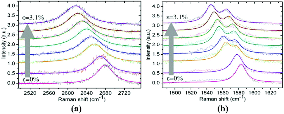 | ||
| Fig. 21 Strain-induced phonon softening of G peak (a) and 2D peak (b) in graphene. Reprinted with permission from ref. 243. Copyright 2009 National Academy of Sciences. | ||
5.3 Thermomechanical properties
Due to the atomically-thin structure of 2DLMs, their mechanical properties are more sensitive to temperature than 3D bulk materials. Theoretically, thermomechanical properties should be investigated under the analysis of the evolution of atomic structures during the change of thermal environments. In general, their in-plane mechanical properties are believed to be softened with the increasing of temperature. This temperature-induced softening can be understood from the following three aspects.132,135,162,173 Firstly, the equilibrium distance between atoms will increase with the increasing temperature, which indicates that the initial bond length is larger at higher temperatures. As a result, it is easier to reach the critical bond length for fracture during tensile deformation. Secondly, the enhanced thermal vibrations of atoms at a higher temperature will induce a larger fluctuation of bond length, thus increasing the possibility of some bonds to reach the critical bond length for breaking. Thirdly, higher temperatures will strengthen the fluctuations of out-of-plane ripples, further weakening the Young's modulus of materials. So far, this temperature-induced softening effect has been reported in graphene,257–259 graphane,111 phosphorene,132 h-BN,135,139 silicene,162 Bi2Te3173 and graphene/silicene/graphene heterostructures.146
5.4 Strain-induced phase transitions
Strain-induced phase transitions of 2DLMs are of great importance in their applications towards phase-change electronics. In contrast to graphene, group VI TMDs usually have more than one possible crystal structure (shown in Fig. 22) consisting of semiconducting phase (2H phase) and metal phase (1T phase and 1T′ phase), but only 2H phase and 1T′ phase are stable without external stabilizing influences.260 Interestingly, group VI TMDs all exhibit 2H phase under ambient conditions except WTe2 which is 1T′ phase.260,261 Theoretical calculations have demonstrated that though the phase transition from 2H phase to 1T′ phase could occur in MoS2, MoSe2, MoTe2, WS2 and WSe2 by biaxial strain, the transition strain may be below but near their breaking thresholds.260,262 While for WTe2, compressive strain could be employed to arouse the phase transition from 1T′ phase to 2H phase.260,262 Due to the lower threshold strain for phase transition, experimental observation of this transition has been reported to be accessible in MoTe2.263 The property that coherent spin transport can occur without heat dissipation in 2D topological insulators makes them ideal materials for dissipationless devices. Previous study has indicated that the monolayer TMDs in 1T′ phase, H′ phase, and T′′ phase were all topological states.264–266 Furthermore, by the introducing of defects and equi-biaxial tensile strain, these 2H-phase TMDs could all be changed into topological insulating states.267 Similarly, the phase transition from ground state to topological phase was theoretically reported to be occurred in few-layers phosphorene under uniaxial compressive strain or vertical tensile strain268 and experimentally observed in bilayer stacked phosphorene under in-plane compressive strain along either zigzag or armchair direction.269 It was interesting to note that this phase transition in bilayer phosphorene also depended on the interlayer stacking order. Besides the transition to topological states, first-principles calculations further revealed that the normal compressive strain or anisotropic biaxial in-plane strain could induce structural transition from pristine Z-phosphorene to A-phosphorene.270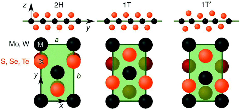 | ||
| Fig. 22 Possible crystal structures of 2D group VI TMDs. Reprinted with permission from ref. 260. Copyright 2014 Springer Nature. | ||
6. Applications
Mechanical and coupling properties of 2DLMs are the cornerstones towards their applications in flexible and novel electronics, which opens the door to achieve reliable and controllable performances in nano-scale devices. Herein, recent achievements in flexible devices based on unique mechanical properties and novel devices based on coupling properties are briefly introduced and summarized.6.1 Electronics based on mechanical properties
Theoretically, the properties of high strain limit (generally larger than 10%, see Fig. 14), high mobility (comparable to Si and even larger271), widely varing electronic properties (from metal to insulator272) and excellent combinability (heterostructural electronics by relatively strong van der Waals interaction137,273,274) generate great interest for the fabrication and application of flexible electronics including transistors, electrodes and photodetectors.Earlier reports on flexible transistors are mainly related to graphene with an ultrahigh mobility of up to 10000 cm2 V−1 s−1.271 Lee and coworkers275 fabricated rugged multi-finger embedded-gate graphene field-effect transistors (EGFET) on flexible polyimide (PI) sheets (shown in Fig. 23(a)) whose robust electrical performance maintained down to a bending radius of ∼1.3 mm corresponding to a bending strain of ∼4.6%. Later report indicated the mechanical robustness of graphene field-effect transistors (GFETs) on flexible PI substrates could be even improved to 0.7 mm bending radius.276 Repeated measurements under the minimum bending radius of 0.7 mm further confirmed its mechanical and electrical reliability. However, the lack of natural bandgap in graphene stimulates the exploration of other 2D layered semiconducting materials, including TMDs (bandgap: 1.06–1.81 eV (ref. 56)) and phosphorene (bandgap: 1.51 eV (ref. 277)). By using mechanically exfoliated MoS2 as channel material, flexible MoS2 transistors on industrial plastic sheets (shown in Fig. 23(b)) were fabricated and exhibited an on/off ratio of larger than 107, a mobility of ∼30 cm2 V−1 s−1 and a subthreshold slope of ∼82 mV per decade in the atmosphere.278 Bending measurements indicated that the deteriorated properties caused by the fracture of dielectrics (Al2O3 and HfO2) only occurred in bending radius smaller than 1 mm. Intriguingly, the interlayer van der Waals interaction of 2D heterostructure is sufficient to maintain their structural stability,38 thus allowing for the fabrication of mechanically reliable heterostructural transistors. Combining the high mobility of graphene and the semiconducting property of MoS2, Yoon et al.273 developed a highly flexible and transparent transistor (shown in Fig. 23(c)) with a high on/off ratio (>104) and an average mobility of ∼4.7 cm2 V−1 s−1 by using CVD grown graphene as source/drain electrodes and exfoliated MoS2 as channels. The electronic properties were stable up to bending radius of ±2.2 mm in compressive and tensile modes, even though a small deterioration was observed after bending cycles of up to 10000 between bending radii of ∞ to 2.7 mm in tensile mode. Furthermore, an ultrathin transistor was developed only by mechanical stacking of conducting graphene (gate electrode), insulating h-BN (dielectric) and semiconducting MoS2 (channel) as shown in Fig. 23(d).137 The resulted mobilities of up to 45 cm2 V−1 s−1 and operating gate voltage below 10 V combined with the excellent electrical robustness upon external strain (up to 1.5%) made it possible for the realization of high-performance flexible and transparent transistors with ultra-small size. Except graphene and TMDs, recent work279 has reported the first flexible field-effect transistor based on few-layer phosphorene, a new semiconducting 2D material, with a maximum carrier mobility of ∼310 cm2 V−1 s−1, which was much larger than ever reported transistors based on MoS2278 and WSe2.274 More importantly, such high mobility was stable up to 2% uniaxial tensile strain and up to 5000 bending cycles.
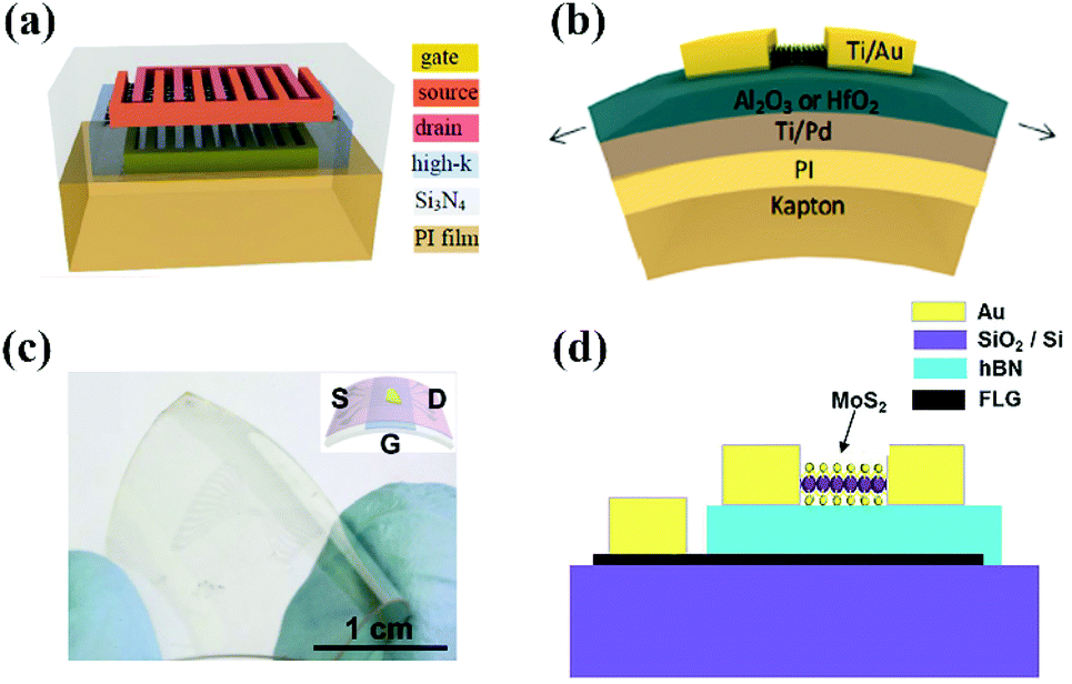 | ||
| Fig. 23 (a) 3D image of multi-finger EGFET of a 10-finger unit cell. (b) Schematic depiction of flexible bottom gate transistor based on MoS2. (c) Photograph image of the highly flexible and transparent MoS2 transistors on a PET substrate. (d) Schematic device structure of transistor by mechanical stacking of graphene, h-BN and MoS2. Reprinted with permission from ref. 275. Copyright 2012 AIP Publishing. Reprinted with permission from ref. 278. Copyright 2013 American Chemical Society. Reprinted with permission from ref. 273. Copyright 2013 John Wiley and Sons. Reprinted with permission from ref. 137. Copyright 2013 American Chemical Society. | ||
For non-transistor applications, graphene has been proved to be ideal candidate for stretchable transparent electrodes with high conductance and high flexibility.49 The resistance of graphene electrode exhibited no evident variation up to bending radius of 2.3 mm corresponding to uniaxial tensile strain of 6.5%, whereas the pre-strained substrates could improve the bending limit up to ∼11%. On the other hand, novel photodetectors with high performance and high flexibility also benefit from the development of 2D layered semiconducting materials. For example, photodetector based on large-area and highly-crystalline WSe2 prepared by pulsed-laser deposition possessed an ultra-broadband detection spectral range from 370 to 1064 nm, reversible photoresponsivity of ∼0.92 A W−1 and external quantum efficiency of up to 180%.138 The corresponding optoelectronic property of the device under constant incident light intensity and various bending radii showed almost no change even at a radius of 5 mm.
6.2 Electronics based on coupling properties
The piezoresistive property of 2DLMs gives rise to ultrathin strain sensor with high flexibility and sensitivity, which can be directly used to detect external strain or pressure. More complicated strain can be detected when strain sensors are fabricated into an array, further demonstrating their applicability in electrical skins for robotics and human body motion monitoring.280–283 Due to the large strain limit, high electrical conductance and excellent transparency of graphene, a great deal of studies on graphene based strain sensors have been carried out. Among these results, their gauge factor differed from −2 to 106 due to the different synthetic methods, substrates, structural forms and so on.284,285 Ahn et al.286 fabricated wafer-scale graphene via CVD method, and the transferred graphene showed a gauge factor (GF) of 6.1. In order to detect the bending motion of a finger, three identical strain sensors in a rosette manner (shown in Fig. 24(a)) were further fabricated on a wearable and stretchable glove, which could simultaneously detect both force and strain direction.287 Zhang et al.288 firstly proposed a charge tunneling model for the piezoresistive effect of a high GF more than 300 in nanographene (NG) films grown in a remote plasma enhanced chemical vapor deposition (RPECVD) system. Intriguingly, different nucleation of NG providing various initial tunneling distances between NG sheets could be tuned by temperature, leading to the GF of NG devices varying from 10 to 103 with the same resistance.289 Besides, they designed periodical ripples of NG to further improve the strain limit (>30%) for flexible electronic applications (shown in Fig. 24(b)).284 On the other hand, Zhu et al. obtained an ultrahigh GF of ∼106 by employing graphene woven fabrics as strain sensors, which could detect weak body motions as electronic skins, including hand clenching, phonation, expression change, blink, breath, and pulse.281,285 For fabricating large-area ultrathin graphene via an environment-friendly and cost-effective method, Zhu et al. proposed a self-assembly process which was rapid and applicable.290 Besides, other efforts have also been proved effect routes to improve the sensitivity and stretchiness of graphene based strain sensors. It was reported that new types of graphene strain sensors based on stretchable yarns could detect both large- and small-scale human motions.291 By using a serpentine-shaped pattern (shown in Fig. 24(c)), the strain sensor was capable of stretching up to 20% with a high GF (42.2) for detecting strain induced by stretching, bending, and torsion.292 Except graphene, strain sensors based on other 2DLMs have been investigated recently, such as MoS2,282,293 α-In2Se3283 and PtSe2.294 Unlike traditional two terminal strain sensor, flexible MoS2 FET strain sensor made the piezoresistivity gate-tunable by more than 1 order of magnitude.293 Furthermore, the electronic-skin based on strain sensor array of MoS2282 (shown in Fig. 24(d)) and α-In2Se3283 both exhibited comparable performances to graphene based electronic-skin. Detail information of these strain sensors discussed above is summarized for comparative analysis in Table 6.
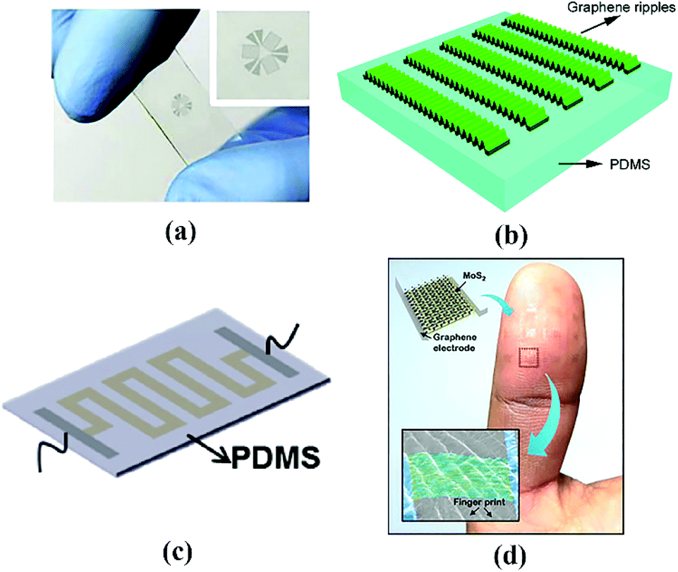 | ||
| Fig. 24 Graphene strain sensor in a rosette manner. (b) Strain sensor based on graphene ripples. (c) Serpentine-shaped graphene strain sensor. (d) Illustration of MoS2-based tactile sensor. Reprinted with permission from ref. 287. Copyright 2013 Elsevier. Reprinted with permission from ref. 284. Copyright 2011 American Chemical Society. Reprinted with permission from ref. 292. Copyright 2017 Elsevier. Reprinted with permission from ref. 282. Copyright 2016 John Wiley and Sons. | ||
| Material | Fabrication method | Dimension (μm × μm) | Layer | Substrate | Strain (%) | GF | Sensitivity (mbar−1) | Ref |
|---|---|---|---|---|---|---|---|---|
| Graphene | CVD | 300 × 140000 | 1 | PDMS | 1 | 6.1 | — | 286 |
| Graphene | Mechanical exfoliation | 1.5 × 22.8 | — | PDMS | 20 | −2 | — | 284 |
| NG | Mechanical exfoliation | — | — | PDMS | 30 | 0.55 | — | 284 |
| Graphene | CVD | 750 × 750 | 1 | SixNy | 2.5 × 10⁻⁴ | 1.8 × 10⁴ | — | 302 |
| NG | RPECVD | 2 × 1400 | — | Mica | 0.3 | 300 | — | 288 |
| Graphene | CVD | — | — | PDMS | 7 | 106 | — | 285 |
| Graphene | CVD | 6 × 64 | 1 | Suspended | 0.29 | 2.92 | 2.96 × 10⁻⁶ | 237 |
| Graphene | CVD | 280 × 280 | Multilayer | SiNx | 0.25 | 1.6 | 6.67 × 10⁻⁶ | 303 |
| Graphene | CVD | — | 10 | PDMS | 2 | 2.4 | — | 287 |
| Graphene | Direct reduction of GO | 20 × 600 | — | PET | — | 9.49 | — | 304 |
| NG | RPECVD | 500 × 500 | — | PDMS | 1 | 500 | — | 289 |
| Graphene | CVD | 490 × 490 | 6 | SiNx | 0.22 | 4.4 | 2.8 × 10⁻⁵ | 305 |
| Graphene | Self-assembly | — | 4.4 nm | PDMS | 2 | 1037 | — | 290 |
| Graphene | CVD | — | 1 | PDMS | 20 | 42.2 | — | 292 |
| MoS2 | Direct sulfurization | — | 3 | Al2O3/ITO/PET | 0.1 | −40 | — | 293 |
| MoS2 | CVD | 1850 × 2100 | 2 | SU-8 | −1.98;1.98 | −72.5; −56.5 | — | 282 |
| α-In2Se3 | CVD | 500 × 1900 | 9.1 nm | PET | 0.39 | 237 | — | 283 |
| PtSe2 | TAC | — | 7–8 | Suspended | — | −84.8 | 5.51 × 10⁻⁴ | 294 |
The piezoelectric properties of 2DLMs have been utilized for the applications of nanogenerator,226,228,230,232,295 phototransistor,296 strain/pressure sensor297 and actuator.298 Previous experiment has demonstrated monolayer MoS2 strained by 0.53% could generate a peak output of 15 mV and 20 pA with a power density of 2 mWm−2 and an energy conversion efficiency of 5.08%.228 When these CVD grown MoS2 flakes were fabricated into array integrations (shown in Fig. 25(a)), great enhancements were acquired in output voltages or currents for four MoS2 nanosheets connected in series or parallel, respectively.228 Besides, the piezoelectric effects in CVD grown MoS2 were reported to be directional dependent, resulting in the two times higher output power of nanogenerator with the armchair direction than with the zigzag direction.230 Though CVD is an ideal method for controllable large-area growth of ultrathin MoS2, sulfur vacancies are inevitable formed to screen piezoelectric polarization charges.295 For improving the performances of CVD grown MoS2 nanogenerator (shown in Fig. 25(b)), sulfur S passivation was proposed and proven to increase the output peak current and voltage by more than 3 times (100 pA) and 2 times (22 mV), respectively.295 Recent observation of the band-piezoelectric effect of biaxial-strained graphene, which arises from the charge transfer along a work function gradient, provides a versatile platform for graphene based nanogenerator.226 The obtained energy conversion efficiency was estimated to be 2.2%. Due to the absent piezoelectric effect in pristine bilayer TMDs, turbostratic stacking was proposed to achieve reliable energy harvesting performance in WSe2 by inducing noncentrosymmetry and increasing mechanical durability.232 The harvesting energy of integrated WSe2 nanogenerators were even able to operate a small liquid crystal display (LCD) without external bias. Further study demonstrated that the piezoelectric effect could be utilized to modulate the carrier dynamics, resulting in strain-gated MoS2 phototransisitor with smallest photocurrent for uniaxial strain of 0.62% and largest photocurrent for uniaxial strain of −0.38%.296 Additionally, the polarization charges could alter the Schottky barrier height on the contacts of MoS2 devices, which was used to realize controllable modulation of the conductivity under strain variation.297 The reliable strain-gating electrical transport gave rise to a new type of MoS2 strain sensor with a high GF of ∼1160. Apart from the in-plane piezoelectricity discussed above, the vertical piezoelectricity in 2DLMs is a key property of their application as actuators with high accuracy of nanometer scale, which is an important part in equipment like force atomic microscopy and scanning tunneling microscopy. Very recent study has measured the vertical piezoelectric coefficient of ultrathin CdS films to be 33 pm V−1.298 The FEM simulation of this novel actuator revealed that the deformation of CdS film was linearly increase from ∼30 to ∼150 pm when the driven voltage varied from −1 to −5 V.
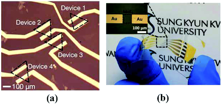 | ||
| Fig. 25 (a) Array integration of CVD single-layer MoS2 flakes as nanogenerators. (b) MoS2 based flexible nanogenerator on a PET substrate. Reprinted with permission from ref. 228. Copyright 2014 Springer Nature. Reprinted with permission from ref. 295. Copyright 2018 John Wiley and Sons. | ||
It was reported that the strain-induced wrinkles of 2DLMs could enhance their photoabsorption because of areal densification, and consequently flexible strain-tunable photoresponsivity could be realized in their photodetectors.299,300 Specially, the enhanced optical extinction by more than 12.5 times accounted for the enhancement of ∼370% in photoresponsivity of crumpled graphene photodetector compared with a flat graphene photodetector.299 Besides, the strain-induced enhanced photoabsorption in MoS2 was also confirmed by ultraviolet–visible spectroscopy.299 Furthermore, the plasmonic enhancement by gold nanoparticle in crumpled graphene could increase the photoresponsivity even by ∼1200%, suggesting the potential applications of this stretchable photodetector as flexible optical sensor and strain sensor.300
7. Conclusions and outlooks
In this review, we have summarized the basic mechanical and coupling properties of novel 2DLMs from comprehensive aspects including characterization methods, intrinsic mechanical properties and behaviour, influence factors, coupling properties and related electronic applications. During the exploration to these atomic thin materials, a great deal of intriguing discoveries have been reached and further stimulated more focus on the fundamental physics and engineering applications. For example, the combined properties of high strength and high flexibility of 2DLMs make them possible not only for the development of flexible and transparent nanodevices based on inorganic low-dimensional materials but also for the regulation of their electronic properties in a relative wide range. Besides, coupling properties between mechanical properties and other physical properties further pave the way to novel nanodevices with unique properties. On the other hand, the close relationship between mechanical properties and internal defects or external environments provides an effective route to tailor 2DLMs with ideal mechanical properties by local regulation or overall regulation.However, the progress made today is far away from the way to final goal. As most studies have demonstrated, perfect 2DLMs always exhibit a brittle behaviour which induces difficulties in their fabrication and usage, because any small defects introduced may cause a great deterioration of strength and failure strain. Even though some efforts have been paid to improve their fracture toughness by defects engineering or chemical functionalization, this problem has not been well solved. Besides, note that some studies have proven that continuum mechanics and related theories are applicable to 2DLMs, but there is still a doubt whether the results from continuum mechanics are reliable for all 2DLMs. And how to bridge the gap between continuum mechanics and atomic level analysis will be the next challenge. In addition, the mechanical properties and mechanical behaviour of graphene, MoS2, h-BN and phosphorene have been investigated systematically, but a great deal of other 2DLMs (more than 30 kinds of 2D materials have been synthesized just for TMDs301) are yet to be studied. Furthermore, some achievements of the coupling properties in this field are proposed only by theoretical analysis without experimental observations, which may be due to the difficulty in experimental operations. So more efforts need to make it clear the real states of coupling properties and make these coupling properties more accessible and controllable in their applications.
Overall, understanding and mastering the mechanical and coupling properties of 2DLMs are of great importance for better design, fabrication and usage of their nanodevices. We hope this review will provide the basic points of progress in this field over the past few years. But it should be noted that more efforts still need to be applied to set up the blocks for this field from fundamental theories and engineering applications.
Conflicts of interest
There are no conflicts to declare.Acknowledgements
This research is financially supported by the National Natural Science Foundation of China (Grant No. 51527901 and 51475256), the National Key Research and Development Program of China (2018YFB2000202), and Beijing National Science Foundation of China (grant no. 3182010).Notes and references
- A. K. Geim and K. S. Novoselov, Nat. Mater., 2007, 6, 183–191 CrossRef CAS PubMed.
- Y. Zhang, Y. W. Tan, H. L. Stormer and P. Kim, Nature, 2005, 438, 201–204 CrossRef CAS PubMed.
- C. Berger, Z. M. Song, X. B. Li, X. S. Wu, N. Brown, C. Naud, D. Mayou, T. B. Li, J. Hass, A. N. Marchenkov, E. H. Conrad, P. First and W. A. D. Heer, Science, 2006, 312, 1191–1196 CrossRef CAS PubMed.
- C. Lee, X. Wei, J. W. Kysar and J. Hone, Science, 2008, 321, 385–388 CrossRef CAS.
- K. Bolotin, K. J. Sikes, Z. F. Jiang, M. Klima, G. Fudenberg, J. Hone, P. Kim and H. L. Stormer, Solid State Commun., 2008, 146, 351–355 CrossRef CAS.
- G. Q. Ning, Z. J. Fan, G. Wang, J. S. Gao, W. Z. Qian and F. Wei, Chem. Commun., 2011, 47, 5976–5978 RSC.
- C. R. Dean, A. F. Young, I. Meric, C. Lee, L. Wang, S. Sorgenfrei, K. Watanabe, T. Taniguchi, P. Kim, K. L. Shepard and J. Hone, Nat. Nanotechnol., 2010, 5, 722–726 CrossRef CAS PubMed.
- T. Palacios, Nat. Nanotechnol., 2011, 6, 464–465 CrossRef CAS PubMed.
- F. N. Xia, T. Mueller, Y. M. Lin, A. V. Garcia and P. Avouris, Nat. Nanotechnol., 2009, 4, 839–843 CrossRef CAS PubMed.
- T. Mueller, F. N. Xia and P. Avouris, Nat. Photonics, 2010, 4, 297–301 CrossRef CAS.
- C. H. Liu, Y. C. Chang, T. B. Norris and Z. H. Zhong, Nat. Nanotechnol., 2014, 9, 273–278 CrossRef CAS PubMed.
- J. S. Bunch, A. M. van der Zande, S. S. Verbridge, I. W. Frank, D. M. Tanenbaum, J. K. Parpia, H. G. Craighead and P. L. McEuen, Science, 2007, 315, 490–493 CrossRef CAS PubMed.
- J. T. Robinson, M. Zalalutdinov, J. W. Baldwin, E. S. Snow, Z. Q. Wei, P. Sheehan and B. H. Houston, Nano Lett., 2008, 8, 3441–3445 CrossRef CAS PubMed.
- C. Y. Chen, S. Rosenblatt, K. I. Bolotin, W. Kalb, P. Kim, I. Kymissis, H. L. Stormer, T. F. Heinz and J. Hone, Nat. Nanotechnol., 2009, 4, 861–867 CrossRef CAS PubMed.
- V. Singh, S. J. Bosman, B. H. Schneider, Y. M. Blanter, A. C. Gomez and G. A. Steele, Nat. Nanotechnol., 2014, 9, 820–824 CrossRef CAS PubMed.
- M. S. Stoller, S. J. Park, Y. W. Zhu, J. H. An and R. S. Ruoff, Nano Lett., 2008, 8, 3498–3502 CrossRef CAS PubMed.
- E. J. Yoo, J. Kim, E. Hosono, H. S. Zhou, T. Kudo and I. Honma, Nano Lett., 2008, 8, 2277–2282 CrossRef CAS PubMed.
- G. X. Wang, X. P. Shen, J. Yao and J. Park, Carbon, 2009, 47, 2049–2053 CrossRef CAS.
- M. A. Rafiee, J. Rafiee, Z. Wang, H. H. Song, Z. Z. Yu and N. Koratkar, ACS Nano, 2009, 3(12), 3884–3890 CrossRef CAS PubMed.
- Z. Xu and C. Gao, Macromolecules, 2010, 43(16), 6716–6723 CrossRef CAS.
- X. Zhao, Q. H. Zhang and D. J. Chen, Macromolecules, 2010, 43, 2357–2363 CrossRef CAS.
- B. Das, K. E. Prasad, U. Ramamurty and C. N. R. Rao, Nanotechnology, 2009, 20, 125705 CrossRef PubMed.
- X. Wang, W. Y. Xing, P. Zhang, L. Song, H. Y. Yang and Y. Hu, Compos. Sci. Technol., 2012, 72, 737–743 CrossRef CAS.
- L. S. Walker, V. R. Marotto, M. A. Rafiee, N. Koratkar and E. L. Corral, ACS Nano, 2011, 5, 3182–3190 CrossRef CAS PubMed.
- L. Kvetková, A. Duszová, P. Hvizdoš, J. Dusza, P. Kun and C. Balázsi, Scr. Mater., 2012, 66, 793–796 CrossRef.
- J. Y. Wang, Z. Q. Li, G. L. Fan, H. H. Pan, Z. X. Chen and D. Zhang, Scr. Mater., 2012, 66, 594–597 CrossRef CAS.
- X. Gao, H. Y. Yue, E. Guo, H. Zhang, X. Y. Lin, L. H. Yao and B. Wang, Mater. Des., 2016, 94, 54–60 CrossRef CAS.
- Y. Han, Z. Xu and C. Gao, Adv. Funct. Mater., 2013, 23, 3693–3700 CrossRef CAS.
- E. J. Duplock, M. Scheffler and P. J. D. Lindan, Phys. Rev. Lett., 2004, 92, 225502 CrossRef PubMed.
- R. Balog, B. Jørgensen, L. Nilsson, M. Andersen, E. Rienks, M. Bianchi, M. Fanetti, E. Lægsgaard, A. Baraldi, S. Lizzit, Z. Sljivancanin, F. Besenbacher, B. Hammer, T. G. Pedersen, P. Hofmann and L. Hornekær, Nat. Mater., 2010, 9, 315–319 CrossRef CAS PubMed.
- Y. B. Zhang, T. T. Tang, C. Girit, Z. Hao, M. C. Martin, A. Zettl, M. F. Crommie, Y. R. Shen and F. Wang, Nature, 2009, 459, 820–823 CrossRef CAS PubMed.
- Z. H. Ni, T. Yu, Y. H. Lu, Y. Y. Wang, Y. P. Feng and Z. X. Shen, ACS Nano, 2008, 2, 2301–2305 CrossRef CAS PubMed.
- G. Cocco, E. Cadelano and L. Colombo, Phys. Rev. B: Condens. Matter Mater. Phys., 2010, 81, 241412 CrossRef.
- S. Park, K. Lee, G. Bozoklu, W. Cai, S. T. Nguyen and R. S. Ruoff, ACS Nano, 2008, 2, 572–578 CrossRef CAS PubMed.
- D. C. Elias, R. R. Nair, T. M. G. Mohiuddin, S. V. Morozov, P. Blake, M. P. Halsall, A. C. Ferrari, D. W. Boukhvalov, M. I. Katsnelson, A. K. Geim and K. S. Novoselov, Science, 2009, 323, 610–613 CrossRef CAS PubMed.
- G. X. Li, Y. L. Li, H. B. Liu, Y. B. Guo, Y. J. Li and D. B. Zhu, Chem. Commun., 2010, 46, 3256–3258 RSC.
- B. G. Kim and H. J. Choi, Phys. Rev. B: Condens. Matter Mater. Phys., 2012, 86, 115435 CrossRef.
- A. K. Geim and I. V. Grigorieva, Nature, 2013, 499, 419–425 CrossRef CAS PubMed.
- Y. W. Zhu, S. Murali, W. W. Cai, X. S. Li, J. W. Suk, J. R. Potts and R. S. Ruoff, Adv. Mater., 2010, 22, 3906–3924 CrossRef CAS PubMed.
- P. Cudazzo, C. Attaccalite, I. V. Tokatly and A. Rubio, Phys. Rev. Lett., 2010, 104, 226804 CrossRef PubMed.
- K. Srinivasu and S. K. Ghosh, J. Phys. Chem. C, 2012, 116, 5951–5956 CrossRef CAS.
- Q. H. Wang, K. K. Zadeh, A. Kis, J. N. Coleman and M. S. Strano, Nat. Nanotechnol., 2012, 7, 699–712 CrossRef CAS PubMed.
- F. N. Xia, H. Wang and Y. C. Jia, Nat. Commun., 2014, 5, 4458 CrossRef CAS PubMed.
- G. H. Lee, Y. J. Yu, C. G. Lee, C. Dean, K. L. Shepard, P. Kim and J. Hone, Appl. Phys. Lett., 2011, 99, 243114 CrossRef.
- H. Wang, F. Liu, W. Fu, Z. Y. Fang, W. Zhou and Z. Liu, Nanoscale, 2014, 6, 12250–12272 RSC.
- C. Zhi, Y. Bando, C. C. Tang, H. Kuwahara and D. Golberg, Adv. Mater., 2009, 21, 2889–2893 CrossRef CAS.
- Y. Wang, Z. X. Shi and J. Yin, J. Mater. Chem., 2011, 21, 11371–11377 RSC.
- A. N. Obraztsov, E. A. Obraztsova, A. V. Tyurnina and A. A. Zolotukhin, Carbon, 2007, 45, 2017–2021 CrossRef CAS.
- K. S. Kim, Y. Zhao, H. Jang, S. Y. Lee, J. M. Kim, K. S. Kim, J. H. Ahn, P. Kim, J. Y. Choi and B. H. Hong, Nature, 2009, 457, 706–710 CrossRef CAS PubMed.
- C. S. Ruiz-Vargas, H. L. Zhuang, P. Y. Huang, A. M. van der Zande, S. Garg, P. L. McEuen, D. A. Muller, R. G. Hennig and J. Park, Nano Lett., 2011, 11, 2259–2263 CrossRef CAS PubMed.
- Z. D. Sha, Q. X. Pei, Y. Y. Zhang and Y. W. Zhang, Nanotechnology, 2016, 27, 315704 CrossRef PubMed.
- F. Banhart, J. Kotakoski and A. V. Krasheninnikov, ACS Nano, 2011, 5, 26–41 CrossRef CAS PubMed.
- Q. B. Zheng, Y. Geng, S. J. Wang, Z. G. Li and J. K. Kim, Carbon, 2010, 48, 4315–4322 CrossRef CAS.
- R. Qin, C. H. Wang, W. J. Zhu and Y. L. Zhang, AIP Adv., 2012, 2, 022159 CrossRef.
- M. Ghorbani-Asl, S. Borini, A. Kuc and T. Heine, Phys. Rev. B: Condens. Matter Mater. Phys., 2013, 87, 235434 CrossRef.
- P. Johari and V. B. Shenoy, ACS Nano, 2012, 6, 5449–5456 CrossRef CAS PubMed.
- R. X. Fei and L. Yang, Nano Lett., 2014, 14, 2884–2889 CrossRef CAS PubMed.
- M. Elahi, K. Khaliji, S. M. Tabatabaei, M. Pourfath and R. Asgari, Phys. Rev. B: Condens. Matter Mater. Phys., 2015, 91, 115412 CrossRef.
- R. Frisenda, M. Drüppel, R. Schmidt, S. M. D. Vasconcellos, D. P. D. Lara, R. Bratschitsch, M. Rohlfing and A. C. Gomez, npj 2D Mater. Appl., 2017, 1, 10 CrossRef.
- R. Biele, E. Flores, J. R. Ares, C. Sanchez, I. J. Ferrer, G. R. Bollinger, A. C. Gomez and R. D'Agosta, Nano Res., 2018, 11, 225–232 CrossRef CAS.
- X. D. Wei, B. Fragneaud, C. A. Marianetti and J. W. Kysar, Phys. Rev. B: Condens. Matter Mater. Phys., 2009, 80, 205407 CrossRef.
- R. C. Cooper, C. Lee, C. A. Marianetti, X. D. Wei, J. Hone and J. W. Kysar, Phys. Rev. B: Condens. Matter Mater. Phys., 2013, 87, 035423 CrossRef.
- A. Castellanos-Gomez, V. Singh, H. S. J. van der Zant and G. A. Steele, Ann. Phys., 2015, 527, 27–44 CrossRef CAS.
- K. Liu and J. Q. Wu, J. Mater. Res., 2016, 31, 832–844 CrossRef CAS.
- D. Akinwande, C. J. Brennan, J. S. Bunch, P. Egberts, J. R. Felts, H. J. Gao, R. Huang, J. S. Kim, T. Li, Y. Li, K. M. Liechti, N. S. Lu, H. S. Park, E. J. Reed, P. Wang, B. I. Yakobson, T. Zhang, Y. W. Zhang, Y. Zhou and Y. Zhu, Extreme Mech. Lett., 2017, 13, 42–77 CrossRef.
- J. H. Kim, J. H. Jeong, N. Kim, R. Joshi and G. H. Lee, J. Phys. D: Appl. Phys., 2018, 52, 083001 CrossRef.
- D. G. Papageorgiou, I. A. Kinloch and R. J. Young, Prog. Mater. Sci., 2017, 90, 75–127 CrossRef CAS.
- C. Androulidakis, K. Zhang, M. Robertson and S. Tawfick, 2D Mater., 2018, 5, 032005 CrossRef.
- J. S. Bunch, S. S. Verbridge, J. S. Alden, A. M. van der Zande, J. M. Parpia, H. G. Craighead and P. L. McEuen, Nano Lett., 2008, 8, 2458–2462 CrossRef CAS PubMed.
- P. Zhang, L. L. Ma, F. F. Fan, Z. Zeng, C. Peng, P. E. Loya, Z. Liu, Y. J. Gong, J. N. Zhang, X. X. Zhang, P. M. Ajayan, T. Zhu and J. Lou, Nat. Commun., 2014, 5, 3782 CrossRef CAS PubMed.
- X. L. Wei, S. Xiao, F. X. Li, D. M. Tang, Q. Chen, Y. Bando and D. Golberg, Nano Lett., 2015, 15, 689–694 CrossRef CAS PubMed.
- C. H. Cao, M. Daly, B. Chen, J. Y. Howe, C. V. Singh, T. Filleter and Y. Sun, Nano Lett., 2015, 15, 6528–6534 CrossRef CAS PubMed.
- S. S. Wang, Z. Qin, G. S. Jung, F. J. M. Martinez, K. Zhang, M. J. Buehler and J. H. Warner, ACS Nano, 2016, 10, 9831–9839 CrossRef CAS PubMed.
- Y. C. Yang, X. Li, M. R. Wen, E. Hacopian, W. B. Chen, Y. J. Gong, J. Zhang, B. Li, W. Zhou, P. M. Ajayan, Q. Chen, T. Zhu and J. Lou, Adv. Mater., 2017, 29, 1604201 CrossRef PubMed.
- C. H. Cao, S. Mukherjee, J. Y. Howe, D. D. Perovic, Y. Sun, C. V. Singh and T. Filleter, Sci. Adv., 2018, 4, eaao7202 CrossRef PubMed.
- I. W. Frank, D. M. Tanenbaum, A. M. van der Zande and P. L. McEuen, J. Vac. Sci. Technol., B: Microelectron. Nanometer Struct. – Process., Meas., Phenom., 2007, 25, 2558 CrossRef CAS.
- C. L. Wong, M. Annamalai, Z. Q. Wang and M. Palaniapan, J. Micromech. Microeng., 2010, 20, 115029 CrossRef.
- J. U. Lee, D. Yoon and H. Cheong, Nano Lett., 2012, 12, 4444–4448 CrossRef CAS PubMed.
- M. F. Yu, O. Lourie, M. J. Dyer, K. Moloni, T. F. Kelly and R. S. Ruoff, Science, 2000, 287, 637–640 CrossRef CAS PubMed.
- M. F. Yu, B. S. Files, S. Arepalli and R. S. Ruoff, Phys. Rev. Lett., 2000, 84, 5552 CrossRef CAS PubMed.
- D. Davidovikj, F. Alijani, S. J. Cartamil-Bueno, H. S. J. van der Zant, M. Amabili and P. G. Steeneken, Nat. Commun., 2017, 8, 1253 CrossRef CAS PubMed.
- J. Tao, W. F. Shen, S. Wu, L. Liu, Z. H. Feng, C. Wang, C. G. Hu, P. Yao, H. Zhang, W. Pang, X. X. Duan, J. Liu, C. W. Zhou and D. H. Zhang, ACS Nano, 2015, 9, 11362–11370 CrossRef CAS PubMed.
- H. Chen, P. Huang, D. Guo and G. X. Xie, J. Phys. Chem. C, 2016, 120, 29491–29497 CrossRef CAS.
- K. Liu, Q. M. Yan, M. Chen, W. Fan, Y. H. Sun, J. Suh, D. Y. Fu, S. Lee, J. Zhou, S. Tongay, J. Ji, J. B. Neaton and J. Q. Wu, Nano Lett., 2014, 14, 5097–5103 CrossRef CAS PubMed.
- A. Castellanos-Gomez, M. Poot, G. A. Steele, H. S. J. van der Zant, N. Agraït and G. Rubio-Bollinger, Adv. Mater., 2012, 24, 772–775 CrossRef CAS PubMed.
- R. J. T. Nicholl, H. J. Conley, N. V. Lavrik, I. Vlassiouk, Y. S. Puzyrev, V. P. Sreenivas, S. T. Pantelides and K. I. Bolotin, Nat. Commun., 2015, 6, 8789 CrossRef CAS PubMed.
- C. Gómez-Navarro, M. Burghard and K. Kern, Nano Lett., 2008, 8, 2045–2049 CrossRef PubMed.
- M. W. Pruessner, T. T. King, D. P. Kelly, R. Grover, L. C. Calhoun and R. Ghodssi, Sens. Actuators, A, 2003, 105, 190–200 CrossRef CAS.
- S. P. Koenig, N. G. Boddeti, M. L. Dunn and J. S. Bunch, Nat. Nanotechnol., 2011, 6, 543–546 CrossRef CAS PubMed.
- S. Jiang, S. Shi and X. Wang, J. Phys. D: Appl. Phys., 2014, 47, 045104 CrossRef.
- J. G. Simmonds, M. R. Begley and U. Komaragiri, J. Appl. Mech., 2005, 72, 203–212 CrossRef.
- L. L. Guo, H. M. Yan, Q. Moore, M. Buettner, J. H. Song, L. Li, P. T. Araujo and H. T. Wang, Nanoscale, 2015, 7, 11915–11921 RSC.
- M. Moreno-Moreno, G. Lopez-Polin, A. Castellanos-Gomez, C. Gomez-Navarro and J. Gomez-Herrero, 2D Mater., 2016, 3, 031007 CrossRef.
- C. Metzger, S. Rémi, M. Liu, S. V. Kusminskiy, A. H. Castro Neto, A. K. Swan and B. B. Goldberg, Nano Lett., 2010, 10, 6–10 CrossRef CAS PubMed.
- M. Goldsche, J. Sonntag, T. Khodkov, G. J. Verbiest, S. Reichardt, C. Neumann, T. Ouaj, N. von den Driesch, D. Buca and C. Stampfer, Nano Lett., 2018, 18, 1707–1713 CrossRef CAS PubMed.
- F. Colangelo, P. Pingue, V. Mišeikis, C. Coletti, F. Beltram and S. Roddaro, 2D Mater., 2019, 6, 025005 CrossRef.
- Y. Sun, K. Liu, X. Hong, M. Chen, J. Kim, S. Shi, J. Wu, A. Zettl and F. Wang, Nano Lett., 2014, 14, 5329–5334 CrossRef CAS PubMed.
- P. Manimunda, Y. Nakanishi, Y. M. Jaques, S. Susarla, C. F. Woellner, S. Bhowmick, S. A. S. Asif, D. S. Galvão, C. S. Tiwary and P. M. Ajayan, 2D Mater., 2017, 4, 045005 CrossRef.
- Y. Li, Z. Hu, S. Lin, S. K. Lai, W. Ji and S. P. Lau, Adv. Funct. Mater., 2017, 27, 1600986 CrossRef.
- M. Huang, H. Yan, T. F. Heinz and J. Hone, Nano Lett., 2010, 10, 4074–4079 CrossRef CAS PubMed.
- P. Lu, X. Wu, W. Guo and X. C. Zeng, Phys. Chem. Chem. Phys., 2012, 14, 13035–13040 RSC.
- S. Yang, C. Wang, H. Sahin, H. Chen, Y. Li, S. Li, A. Suslu, F. M. Peeters, Q. Liu, J. Li and S. Tongay, Nano Lett., 2015, 15, 1660–1666 CrossRef CAS PubMed.
- J. W. Suk, R. D. Piner, J. An and R. S. Ruoff, ACS Nano, 2010, 4, 6557–6564 CrossRef CAS PubMed.
- K. N. Spanos, S. K. Georgantzinos and N. K. Anifantis, Compos. Struct., 2015, 132, 536–544 CrossRef.
- A. Falin, Q. Cai, E. J. G. Santos, D. Scullion, D. Qian, R. Zhang, Z. Yang, S. Huang, K. Watanabe, T. Taniguchi, M. R. Barnett, Y. Chen, R. S. Ruoff and L. H. Li, Nat. Commun., 2017, 8, 15815 CrossRef CAS PubMed.
- G. López-Polín, M. Jaafar, F. Guinea, R. Roldán, C. Gómez-Navarro and J. Gómez-Herrero, Carbon, 2017, 124, 42–48 CrossRef.
- R. Grantab, V. B. Shenoy and R. S. Ruoff, Science, 2010, 330, 946–948 CrossRef CAS PubMed.
- Q. X. Pei, Y. W. Zhang and V. B. Shenoy, Carbon, 2010, 48, 898–904 CrossRef CAS.
- Q. X. Pei, Y. W. Zhang and V. B. Shenoy, Nanotechnology, 2010, 21, 115709 CrossRef PubMed.
- Y. Pei, Phys. B, 2012, 407, 4436–4439 CrossRef CAS.
- M. Topsakal, S. Cahangirov and S. Ciraci, Appl. Phys. Lett., 2010, 96, 091912 CrossRef.
- Q. Peng, W. Ji and S. De, Phys. Chem. Chem. Phys., 2012, 14, 13385–13391 RSC.
- Q. Peng, W. Ji and S. De, Comput. Mater. Sci., 2012, 56, 11–17 CrossRef CAS.
- E. Torun, H. Sahin, S. Cahangirov, A. Rubio and F. M. Peeters, J. Appl. Phys., 2016, 119, 074307 CrossRef.
- Q. Wei and X. Peng, Appl. Phys. Lett., 2014, 104, 251915 CrossRef.
- J. H. Zhao, N. Wei, Z. Y. Fan, J. W. Jiang and T. Rabczuk, Nanotechnology, 2013, 24, 095702 CrossRef PubMed.
- Q. Peng and S. De, Phys. Chem. Chem. Phys., 2013, 15, 19427–19437 RSC.
- L. Xu, N. Wei and Y. Zheng, Nanotechnology, 2013, 24, 505703 CrossRef PubMed.
- C. Carpenter, D. Maroudas and A. Ramasubramaniam, Appl. Phys. Lett., 2013, 103, 013102 CrossRef.
- S. Zhao and J. Xue, J. Phys. D: Appl. Phys., 2013, 46, 135303 CrossRef.
- A. H. C. Neto, F. Guinea, N. M. R. Peres, K. S. Novoselov and A. K. Geim, Rev. Mod. Phys., 2009, 81, 109 CrossRef.
- G. López-Polín, C. Gómez-Navarro, V. Parente, F. Guinea, M. I. Katsnelson, F. Pérez-Murano and J. Gómez-Herrero, Nat. Phys., 2015, 11, 26–31 Search PubMed.
- F. Hao, D. Fang and Z. Xu, Appl. Phys. Lett., 2011, 99, 041901 CrossRef.
- N. K. Perkgöz and C. Sevik, Nanotechnology, 2014, 25, 185701 CrossRef PubMed.
- J. Hou, Z. N. Yin, Y. Y. Zhang and T. C. Chang, Acta Mech. Sin., 2016, 32, 684–689 CrossRef CAS.
- J. X. Qu, H. W. Zhang, J. X. Li, S. X. Zhao and T. Chang, Carbon, 2017, 120, 350–357 CrossRef CAS.
- J. Hou, Z. N. Yin, Y. Y. Zhang and T. Chang, J. Appl. Mech., 2015, 82, 094501 CrossRef.
- Y. Y. Zhang, Q. X. Pei and C. M. Wang, Appl. Phys. Lett., 2012, 101, 081909 CrossRef.
- J. O. Sofo, A. S. Chaudhari and G. D. Barber, Phys. Rev. B: Condens. Matter Mater. Phys., 2007, 75, 153401 CrossRef.
- P. Vogt, P. D. Padova, C. Quaresima, J. Avila, E. Frantzeskakis, M. C. Asensio, A. Resta, B. Ealet and G. L. Lay, Phys. Rev. Lett., 2012, 108, 155501 CrossRef PubMed.
- S. Rudorf and T. A. Hare, Superlattices Microstruct., 2014, 65, 64–70 CrossRef.
- Z. D. Sha, Q. X. Pei, Z. W. Ding, J. W. Jiang and Y. W. Zhang, J. Phys. D: Appl. Phys., 2015, 48, 395303 CrossRef.
- L. Song, L. J. Ci, H. Lu, P. B. Sorokin, C. H. Jin, J. Ni, A. G. Kvashnin, D. G. Kvashnin, J. Lou, B. I. Yakobson and P. M. Ajayan, Nano Lett., 2010, 10, 3209–3215 CrossRef CAS PubMed.
- J. W. Jiang and H. S. Park, Nat. Commun., 2014, 5, 4727 CrossRef CAS PubMed.
- S. Thomas, K. M. Ajith and V. Cheruvalath, Mater. Res. Express, 2017, 4, 065005 CrossRef.
- S. Thomas, K. M. Ajith and M. C. Valsakumar, J. Phys.: Condens. Matter, 2016, 28, 295302 CrossRef PubMed.
- G. H. Lee, Y. J. Yu, X. Cui, N. Petrone, C. H. Lee, M. S. Choi, D. Y. Lee, C. Lee, W. J. Yoo, K. Watanabe, T. Taniguchi, C. Nuckolls, P. Kim and J. Hone, ACS Nano, 2013, 7, 7931–7936 CrossRef CAS PubMed.
- Z. Q. Zheng, T. M. Zhang, J. Yao, Y. Zhang, J. Xu and G. W. Yang, Nanotechnology, 2016, 27, 225501 CrossRef PubMed.
- L. Cheng, W. J. Huang, Q. F. Gong, C. H. Liu, Z. Liu, Y. G. Li and H. J. Dai, Angew. Chem., Int. Ed., 2014, 53, 7860–7863 CrossRef CAS PubMed.
- C. Xu, L. B. Wang, Z. B. Liu, L. Chen, J. K. Guo, N. Kang, X. L. Ma, H. M. Cheng and W. C. Ren, Nat. Mater., 2015, 14, 1135–1141 CrossRef CAS PubMed.
- T. Li, Phys. Rev. B: Condens. Matter Mater. Phys., 2012, 85, 235407 CrossRef.
- S. Bertolazzi, J. Brivio and A. Kis, ACS Nano, 2011, 5, 9703–9709 CrossRef CAS PubMed.
- J. L. Feldman, J. Phys. Chem. Solids, 1976, 37, 1141–1144 CrossRef CAS.
- B. Mortazavi, M. Shahrokhi, M. Makaremi and T. Rabczuk, Nanotechnology, 2017, 28, 115705 CrossRef PubMed.
- J. W. Jiang and H. S. Park, Appl. Phys. Lett., 2014, 105, 033108 CrossRef.
- J. Y. Chung, V. Sorkin, Q. X. Pei, C. H. Chiu and Y. W. Zhang, J. Phys. D: Appl. Phys., 2017, 50, 345302 CrossRef.
- A. A. Griffith, Philos. Trans. R. Soc. London, 1921, 221, 163–198 CrossRef.
- S. W. Cranford and M. J. Buehler, Carbon, 2011, 49, 4111–4121 CrossRef CAS.
- P. R. Budarapu, B. Javvaji, V. K. Sutrakar, D. R. Mahapatra, M. Paggi, G. Zi and T. Rabczuk, Int. J. Fract., 2017, 203, 81–98 CrossRef CAS.
- K. Kim, V. I. Artyukhov, W. Regan, Y. Y. Liu, M. F. Crommie, B. I. Yakobson and A. Zettl, Nano Lett., 2012, 12, 293–297 CrossRef CAS PubMed.
- C. A. Marianetti and H. G. Yevick, Phys. Rev. Lett., 2010, 105, 245502 CrossRef CAS PubMed.
- F. Liu, P. Ming and J. Li, Phys. Rev. B: Condens. Matter Mater. Phys., 2007, 76, 064120 CrossRef.
- H. D. Wang, X. X. Li, P. Li and J. L. Yang, Nanoscale, 2017, 9, 850–855 RSC.
- F. Traversi, F. J. Gúzman-Vázquez, L. G. Rizzi, V. Russo, C. S. Casari, C. Gómez-Navarro and R. Sordan, New J. Phys., 2010, 12, 023034 CrossRef.
- G. H. Lee, R. C. Cooper, S. J. An, S. Lee, A. van der Zande, N. Petrone, A. G. Hammerberg, C. Lee, B. Crawford, W. Oliver, J. W. Kysar and J. Hone, Science, 2013, 340, 1073–1076 CrossRef CAS PubMed.
- Y. Y. Zhang, C. M. Wang, Y. Cheng and Y. Xiang, Carbon, 2011, 49, 4511–4517 CrossRef CAS.
- K. N. Kudin, G. E. Scuseria and B. I. Yakobson, Phys. Rev. B: Condens. Matter Mater. Phys., 2001, 64, 235406 CrossRef.
- H. Şahin, S. Cahangirov, M. Topsakal, E. Bekaroglu, E. Akturk, R. T. Senger and S. Ciraci, Phys. Rev. B: Condens. Matter Mater. Phys., 2009, 80, 155453 CrossRef.
- R. C. Andrew, R. E. Mapasha, A. M. Ukpong and N. Chetty, Phys. Rev. B: Condens. Matter Mater. Phys., 2012, 85, 125428 CrossRef.
- C. H. Cao, M. Daly, C. V. Singh, Y. Sun and T. Filleter, Carbon, 2015, 81, 497–504 CrossRef CAS.
- L. Z. Liu, J. F. Zhang, J. J. Zhao and F. Liu, Nanoscale, 2012, 4, 5910–5916 RSC.
- Q. X. Pei, Z. D. Sha, Y. Y. Zhang and Y. W. Zhang, J. Appl. Phys., 2014, 115, 023519 CrossRef.
- H. Zhao, Phys. Lett. A, 2012, 376, 3546–3550 CrossRef CAS.
- Q. Peng, X. Wen and S. De, RSC Adv., 2013, 3, 13772–13781 RSC.
- J. W. Jiang and H. S. Park, J. Phys. D: Appl. Phys., 2014, 47, 385304 CrossRef.
- L. Q. Wang, A. Kutana, X. L. Zou and B. I. Yakobson, Nanoscale, 2015, 7, 9746–9751 RSC.
- Q. L. Xiong, Z. H. Li and X. G. Tian, J. Phys. D: Appl. Phys., 2015, 48, 375502 CrossRef.
- B. Mortazavi and Y. Rémond, Physica E, 2012, 44, 1846–1852 CrossRef CAS.
- T. Han, Y. Luo and C. Wang, J. Phys. D: Appl. Phys., 2014, 47, 25303 CrossRef.
- J. T. Wu, B. L. Wang, Y. J. Wei, R. G. Yang and M. Dresselhaus, Mater. Res. Lett., 2013, 1, 200–206 CrossRef CAS.
- J. W. Jiang, Nanotechnology, 2015, 26, 315706 CrossRef PubMed.
- A. Kumar and P. K. Ahluwalia, Physica B, 2013, 419, 66–75 CrossRef CAS.
- Y. Tong, F. J. Yi, L. S. Liu, P. C. Zhai and Q. J. Zhang, Physica B, 2010, 405, 3190–3194 CrossRef CAS.
- L. C. He, S. Guo, J. C. Lei, Z. D. Sha and Z. S. Liu, Carbon, 2014, 75, 124–132 CrossRef CAS.
- Y. Y. Liu, F. B. Xu, Z. Zhang, E. S. Penev and B. I. Yakobson, Nano Lett., 2014, 14, 6782–6786 CrossRef CAS PubMed.
- W. Zhou, X. L. Zou, S. Najmaei, Z. Liu, Y. M. Shi, J. Kong, J. Lou, P. M. Ajayan, B. I. Yakobson and J. C. Idrobo, Nano Lett., 2013, 13, 2615–2622 CrossRef CAS PubMed.
- O. V. Yazyev and S. G. Louie, Phys. Rev. B: Condens. Matter Mater. Phys., 2010, 81, 195420 CrossRef.
- X. L. Zou, Y. Y. Liu and B. I. Yakobson, Nano Lett., 2013, 13, 253–258 CrossRef CAS PubMed.
- Y. Y. Liu, X. L. Zou and B. I. Yakobson, ACS Nano, 2012, 6, 7053–7058 CrossRef CAS PubMed.
- Y. J. Wei, J. T. Wu, H. Q. Yin, X. H. Shi, R. G. Yang and M. Dresselhaus, Nat. Mater., 2012, 11, 759–763 CrossRef CAS PubMed.
- Z. G. Song, V. I. Artyukhov, B. I. Yakobson and Z. P. Xu, Nano Lett., 2013, 13, 1829–1833 CrossRef CAS PubMed.
- K. Q. Dang and D. E. Spearot, J. Appl. Phys., 2014, 116, 013508 CrossRef.
- S. Eigler, M. Enzelberger-Heim, S. Grimm, P. Hofmann, W. Kroener, A. Geworski, C. Dotzer, M. Röckert, J. Xiao, C. Papp, O. Lytken, H. P. Steinrück, P. Müller and A. Hirsch, Adv. Mater., 2013, 25, 3583–3587 CrossRef CAS PubMed.
- R. T. Lv, J. A. Robinson, R. E. Schaak, D. Sun, Y. F. Sun, T. E. Mallouk and M. Terrones, Acc. Chem. Res., 2015, 48, 56–64 CrossRef CAS PubMed.
- Y. Lu, B. R. Goldsmith, N. J. Kybert and A. T. C. Johnson, Appl. Phys. Lett., 2010, 97, 083107 CrossRef.
- P. K. Kannan, D. J. Late, H. Morgan and C. S. Rout, Nanoscale, 2015, 7, 13293–13312 RSC.
- W. W. Cai, R. D. Piner, F. J. Stadermann, S. Park, M. A. Shaibat, Y. Ishii, D. X. Yang, A. Velamakanni, S. J. An, M. Stoller, J. An, D. M. Chen and R. S. Ruoff, Science, 2008, 321, 1815–1817 CrossRef CAS PubMed.
- J. C. Meyer, A. K. Geim, M. I. Katsnelson, K. S. Novoselov, T. J. Booth and S. Roth, Nature, 2007, 446, 60–63 CrossRef CAS PubMed.
- J. Brivio, D. T. L. Alexander and A. Kis, Nano Lett., 2011, 11, 5148–5153 CrossRef CAS PubMed.
- H. X. Zhang and P. X. Feng, ACS Appl. Mater. Interfaces, 2012, 4, 30–33 CrossRef CAS PubMed.
- Z. T. Luo, Y. Lu, D. W. Singer, M. E. Berck, L. A. Somers, B. R. Goldsmith and A. T. C. Johnson, Chem. Mater., 2011, 23, 1441–1447 CrossRef CAS.
- K. K. Kim, A. Hsu, X. T. Jia, S. M. Kim, Y. M. Shi, M. Hofmann, D. Nezich, J. F. Rodriguez-Nieva, M. Dresselhaus, T. Palacios and J. Kong, Nano Lett., 2012, 12, 161–166 CrossRef PubMed.
- R. Y. Tay, M. H. Griep, G. Mallick, S. H. Tsang, R. S. Singh, T. Tumlin, E. H. T. Teo and S. P. Karna, Nano Lett., 2014, 14, 839–846 CrossRef CAS PubMed.
- K. H. Lee, H. J. Shin, J. Lee, I. Lee, G. H. Kim, J. Y. Choi and S. W. Kim, Nano Lett., 2012, 12, 714–718 CrossRef CAS PubMed.
- B. Zhang, W. H. Lee, R. Piner, I. Kholmanov, Y. P. Wu, H. F. Li, H. X. Ji and R. S. Ruoff, ACS Nano, 2012, 6, 2471–2476 CrossRef CAS PubMed.
- M. H. Griep, E. Sandoz-Rosado, T. M. Tumlin and E. Wetzel, Nano Lett., 2016, 16, 1657–1662 CrossRef CAS PubMed.
- J. O. Island, G. A. Steele, H. S. J. van der Zant and A. Castellanos-Gomez, 2D Mater., 2015, 2, 011002 CrossRef.
- J. D. Wood, S. A. Wells, D. Jariwala, K. S. Chen, E. Cho, V. K. Sangwan, X. L. Liu, L. J. Lauhon, T. J. Marks and M. C. Hersam, Nano Lett., 2014, 14, 6964–6970 CrossRef CAS PubMed.
- Z. Wang, L. Philippe and J. Elias, Phys. Rev. B: Condens. Matter Mater. Phys., 2010, 81, 155405 CrossRef.
- Z. Wang, Carbon, 2009, 47, 3050–3053 CrossRef CAS.
- Z. Osváth, F. Lefloch, V. Bouchiat and C. Chapelier, Nanoscale, 2013, 5, 10996–11002 RSC.
- P. Hao, Y. W. Gao and Y. H. Zhou, Sci. China: Phys., Mech. Astron., 2013, 56, 1148–1156 CAS.
- Q. Lu and R. Huang, Int. J. Appl. Mech., 2009, 1, 443–467 CrossRef.
- P. Huang, D. Guo, G. X. Xie and J. Li, Nano Lett., 2017, 17, 6280–6286 CrossRef CAS PubMed.
- V. M. Pereira and A. H. C. Neto, Phys. Rev. Lett., 2009, 103, 046801 CrossRef PubMed.
- F. Guinea, M. I. Katsnelson and A. K. Geim, Nat. Phys., 2010, 6, 30–33 Search PubMed.
- A. Castellanos-Gomez, R. Roldán, E. Cappelluti, M. Buscema, F. Guinea, H. S. J. van der Zant and G. A. Steele, Nano Lett., 2013, 13, 5361–5366 CrossRef CAS PubMed.
- A. P. Nayak, S. Bhattacharyya, J. Zhu, J. Liu, X. Wu, T. Pandey, C. Q. Jin, A. K. Singh, D. Akinwande and J. F. Lin, Nat. Commun., 2014, 5, 3731 CrossRef CAS PubMed.
- L. Kou, C. Tang, W. Guo and C. Chen, ACS Nano, 2011, 5, 1012–1017 CrossRef CAS PubMed.
- Y. Ma, Y. Dai, M. Guo, C. Niu, L. Yu and B. Huang, Nanoscale, 2011, 3, 2301–2306 RSC.
- Y. D. Ma, Y. Dai, M. Guo, C. W. Niu, Y. T. Zhu and B. B. Huang, ACS Nano, 2012, 6, 1695–1701 CrossRef CAS PubMed.
- A. D. Smith, F. Niklaus, A. Paussa, S. Schröder, A. C. Fischer, M. Sterner, S. Wagner, S. Vaziri, F. Forsberg, D. Esseni, M. Östling and M. C. Lemme, ACS Nano, 2016, 10, 9879–9886 CrossRef CAS PubMed.
- A. D. Smith, F. Niklaus, A. Paussa, S. Vaziri, A. C. Fischer, M. Sterner, F. Forsberg, A. Delin, D. Esseni, P. Palestri, M. Östling and M. C. Lemme, Nano Lett., 2013, 13, 3237–3242 CrossRef CAS PubMed.
- X. W. Fu, Z. M. Liao, J. X. Zhou, Y. B. Zhou, H. C. Wu, R. Zhang, G. Jing, J. Xu, X. Wu, W. Guo and D. Yu, Appl. Phys. Lett., 2011, 99, 213107 CrossRef.
- S. Manzeli, A. Allain, A. Ghadimi and A. Kis, Nano Lett., 2015, 15, 5330–5335 CrossRef CAS PubMed.
- Z. Zhang, L. Li, J. Horng, N. Z. Wang, F. Yang, Y. Yu, Y. Zhang, G. Chen, K. Watanabe, T. Taniguchi, X. H. Chen, F. Wang and Y. Zhang, Nano Lett., 2017, 17, 6097–6103 CrossRef CAS PubMed.
- C. An, Z. Xu, W. Shen, R. Zhang, Z. Sun, S. Tang, Y. Xiao, D. Zhang, D. Sun, X. Hu, C. Hu, L. Yang and J. Liu, ACS Nano, 2019, 13, 3310–3319 CrossRef CAS PubMed.
- X. D. Wang, J. Zhou, J. H. Song, J. Liu, N. S. Xu and Z. L. Wang, Nano Lett., 2006, 6, 2768–2772 CrossRef CAS PubMed.
- R. Yang, Y. Qin, L. Dai and Z. L. Wang, Nat. Nanotechnol., 2009, 4, 34–39 CrossRef CAS PubMed.
- K. H. Michel and B. Verberck, Phys. Rev. B: Condens. Matter Mater. Phys., 2009, 80, 224301 CrossRef.
- K. A. N. Duerloo, M. T. Ong and E. J. Reed, J. Phys. Chem. Lett., 2012, 3, 2871–2876 CrossRef CAS.
- R. X. Fei, W. B. Li, J. Li and L. Yang, Appl. Phys. Lett., 2015, 107, 173104 CrossRef.
- H. L. Zhuang, M. D. Johannes, M. N. Blonsky and R. G. Hennig, Appl. Phys. Lett., 2014, 104, 022116 CrossRef.
- M. N. Blonsky, H. L. Zhuang, A. K. Singh and R. G. Hennig, ACS Nano, 2015, 9, 9885–9891 CrossRef CAS PubMed.
- M. T. Ong and E. J. Reed, ACS Nano, 2012, 6, 1387–1394 CrossRef CAS PubMed.
- X. Wang, H. Tian, W. Xie, Y. Shu, W. T. Mi, M. A. Mohammad, Q. Y. Xie, Y. Yang, J. B. Xu and T. L. Ren, NPG Asia Mater., 2015, 7, e154 CrossRef CAS.
- G. da Cunha Rodrigues, P. Zelenovskiy, K. Romanyuk, S. Luchkin, Y. Kopelevich and A. Kholkin, Nat. Commun., 2015, 6, 7572 CrossRef PubMed.
- W. Z. Wu, L. Wang, Y. L. Li, F. Zhang, L. Lin, S. M. Niu, D. Chenet, X. Zhang, Y. F. Hao, T. F. Heinz, J. Hone and Z. L. Wang, Nature, 2014, 514, 470–474 CrossRef CAS PubMed.
- H. Zhu, Y. Wang, J. Xiao, M. Liu, S. Xiong, Z. J. Wong, Z. Ye, Y. Ye, X. Yin and X. Zhang, Nat. Nanotechnol., 2015, 10, 151–155 CrossRef CAS PubMed.
- S. K. Kim, R. Bhatia, T. H. Kim, D. Seol, J. H. Kim, H. Kim, W. Seung, Y. Kim, Y. H. Lee and Sa. W. Kim, Nano Energy, 2016, 22, 483–489 CrossRef CAS.
- E. N. Esfahani, T. Li, B. Huang, X. Xu and J. Li, Nano Energy, 2018, 52, 117–122 CrossRef.
- J. H. Lee, J. Y. Park, E. B. Cho, T. Y. Kim, S. A. Han, T. H. Kim, Y. Liu, S. K. Kim, C. J. Roh, H. J. Yoon, H. Ryu, W. Seung, J. S. Lee, J. Lee and S. W. Kim, Adv. Mater., 2017, 29, 1606667 CrossRef PubMed.
- R. R. Nair, P. Blake, A. N. Grigorenko, K. S. Novoselov, T. J. Booth, T. Stauber, N. M. R. Peres and A. K. Geim, Science, 2008, 320, 1308–1308 CrossRef CAS PubMed.
- V. M. Pereira, R. M. Ribeiro, N. M. R. Peres and A. H. C. Neto, Europhys. Lett., 2011, 92, 67001 CrossRef.
- G. X. Ni, H. Z. Yang, W. Ji, S. J. Baeck, C. T. Toh, J. H. Ahn, V. M. Pereira and B. Özyilmaz, Adv. Mater., 2014, 26, 1081–1086 CrossRef CAS PubMed.
- M. O. Leyva and G. G. Naumis, 2D Mater., 2015, 2, 025001 CrossRef.
- F. Kafi, R. P. Shahri, M. R. Benam and A. Akhtar, J. Electron. Mater., 2017, 46, 6158–6166 CrossRef CAS.
- S. Deng, Y. Zhang and L. Li, Appl. Surf. Sci., 2019, 476, 308–316 CrossRef CAS.
- A. C. Ferrari, J. C. Meyer, V. Scardaci, C. Casiraghi, M. Lazzeri, F. Mauri, S. Piscanec, D. Jiang, K. S. Novoselov, S. Roth and A. K. Geim, Phys. Rev. Lett., 2006, 97, 187401 CrossRef CAS PubMed.
- O. Frank, G. Tsoukleri, J. Parthenios, K. Papagelis, I. Riaz, R. Jalil, K. S. Novoselov and C. Galiotis, ACS Nano, 2010, 4, 3131–3138 CrossRef CAS PubMed.
- T. M. G. Mohiuddin, A. Lombardo, R. R. Nair, A. Bonetti, G. Savini, R. Jalil, N. Bonini, D. M. Basko, C. Galiotis, N. Marzari, K. S. Novoselov, A. K. Geim and A. C. Ferrari, Phys. Rev. B: Condens. Matter Mater. Phys., 2009, 79, 205433 CrossRef.
- O. Frank, M. Mohr, J. Maultzsch, C. Thomsen, I. Riaz, R. Jalil, K. S. Novoselov, G. Tsoukleri, J. Parthenios, K. Papagelis, L. Kavan and C. Galiotis, ACS Nano, 2011, 5, 2231–2239 CrossRef CAS PubMed.
- M. Huang, H. Yan, C. Chen, D. Song, T. F. Heinz and J. Hone, Proc. Natl. Acad. Sci. U. S. A., 2009, 106, 7304–7308 CrossRef CAS PubMed.
- M. Yagmurcukardes, C. Bacaksiz, E. Unsal, B. Akbali, R. T. Senger and H. Sahin, Phys. Rev. B: Condens. Matter Mater. Phys., 2018, 97, 115427 CrossRef CAS.
- T. J. Wieting and J. L. Verble, Phys. Rev. B: Condens. Matter Mater. Phys., 1971, 3, 4286 CrossRef.
- J. M. Chen and C. S. Wang, Solid State Commun., 1974, 14, 857–860 CrossRef CAS.
- Y. Wang, C. Cong, C. Qiu and T. Yu, Small, 2013, 9, 2857–2861 CrossRef CAS PubMed.
- C. Rice, R. J. Young, R. Zan and U. Bangert, Phys. Rev. B: Condens. Matter Mater. Phys., 2013, 87, 081307 CrossRef.
- H. J. Conley, B. Wang, J. I. Ziegler, R. F. Haglund Jr., S. T. Pantelides and K. I. Bolotin, Nano Lett., 2013, 13, 3626–3630 CrossRef CAS PubMed.
- Y. Wang, C. Cong, W. Yang, J. Shang, N. Peimyoo, Y. Chen, J. Kang, J. Wang, W. Huang and T. Yu, Nano Res., 2015, 8, 2562–2572 CrossRef CAS.
- S. Sugai and I. Shirotani, Solid State Commun., 1985, 53, 753–755 CrossRef CAS.
- X. Ling, L. Liang, S. Huang, A. A. Puretzky, D. B. Geohegan, B. G. Sumpter, J. Kong, V. Meunier and M. S. Dresselhaus, Nano Lett., 2015, 15, 4080–4088 CrossRef CAS PubMed.
- J. X. Wu, N. N. Mao, L. M. Xie, H. Xu and J. Zhang, Angew. Chem., Int. Ed., 2015, 54, 2366–2369 CrossRef CAS PubMed.
- H. B. Ribeiro, M. A. de Pimenta, C. J. S. de Matos, R. L. Moreira, A. S. Rodin, J. D. Zapata, E. A. T. de Souza and A. H. Castro Neto, ACS Nano, 2015, 9, 4270–4276 CrossRef CAS PubMed.
- Y. Wang, C. Cong, R. Fei, W. Yang, Y. Chen, B. Cao, L. Yang and T. Yu, Nano Res., 2015, 8, 3944–3953 CrossRef CAS.
- S. Zhang, N. Mao, J. Wu, L. Tong, J. Zhang and Z. Liu, Small, 2017, 13, 1700466 CrossRef PubMed.
- H. Zhao and N. R. Aluru, J. Appl. Phys., 2010, 108, 064321 CrossRef.
- S. Chen and D. C. Chrzan, Phys. Rev. B: Condens. Matter Mater. Phys., 2011, 84, 195409 CrossRef.
- W. Gao and R. Huang, J. Mech. Phys. Solids, 2014, 66, 42–58 CrossRef CAS.
- K. A. N. Duerloo, Y. Li and E. J. Reed, Nat. Commun., 2014, 5, 4214 CrossRef CAS PubMed.
- J. A. Wilson and A. D. Yoffe, Adv. Phys., 1969, 18, 193–335 CrossRef CAS.
- H. H. Huang, X. Fan, D. J. Singh, H. Chen, Q. Jiang and W. T. Zheng, Phys. Chem. Chem. Phys., 2016, 18, 4086–4094 RSC.
- S. Song, D. H. Keum, S. Cho, D. Perello, Y. Kim and Y. H. Lee, Nano Lett., 2016, 16, 188–193 CrossRef CAS PubMed.
- X. Qian, J. Liu, L. Fu and J. Li, Science, 2014, 346, 1344–1347 CrossRef CAS PubMed.
- Y. Ma, L. Kou, X. Li, Y. Dai and T. Heine, Phys. Rev. B: Condens. Matter Mater. Phys., 2016, 93, 035442 CrossRef.
- F. Ma, G. Gao, Y. Jiao, Y. Gu, A. Bilic, H. Zhang, Z. Chen and A. Du, Nanoscale, 2016, 8, 4969–4975 RSC.
- X. Li, S. Zhang and Q. Wang, Nanoscale, 2017, 9, 562–569 RSC.
- E. T. Sisakht, F. Fazileh, M. H. Zare, M. Zarenia and F. M. Peeters, Phys. Rev. B: Condens. Matter Mater. Phys., 2016, 94, 085417 CrossRef.
- T. Zhang, J. H. Lin, Y. M. Yu, X. R. Chen and W. M. Liu, Sci. Rep., 2015, 5, 13927 CrossRef CAS PubMed.
- T. Hu and J. Dong, Phys. Rev. B: Condens. Matter Mater. Phys., 2015, 92, 064114 CrossRef.
- D. Akinwande, N. Petrone and J. Hone, Nat. Commun., 2014, 5, 5678 CrossRef CAS PubMed.
- C. Lee, Q. Y. Li, W. Kalb, X. Z. Liu, H. Berger, R. W. Carpick and J. Hone, Science, 2010, 328, 76–80 CrossRef CAS PubMed.
- J. Yoon, W. Park, G. Y. Bae, Y. Kim, H. S. Jang, Y. Hyun, S. K. Lim, Y. H. Kahng, W. K. Hong, B. H. Lee and H. C. Ko, Small, 2013, 9, 3295–3300 CAS.
- S. Das, R. Gulotty, A. V. Sumant and A. Roelofs, Nano Lett., 2014, 14, 2861–2866 CrossRef CAS PubMed.
- J. Lee, L. Tao, K. N. Parrish, Y. F. Hao, R. S. Ruoff and D. Akinwande, Appl. Phys. Lett., 2012, 101, 252109 CrossRef.
- J. Lee, T. J. Ha, H. F. Li, K. N. Parrish, M. Holt, A. Dodabalapur, R. S. Ruoff and D. Akinwand, ACS Nano, 2013, 7, 7744–7750 CrossRef CAS PubMed.
- J. S. Qiao, X. H. Kong, Z. X. Hu, F. Yang and W. Ji, Nat. Commun., 2014, 5, 4475 CrossRef CAS PubMed.
- H. Y. Chang, S. X. Yang, J. Lee, L. Tao, W. S. Hwang, D. Jena, N. S. Lu and D. Akinwande, ACS Nano, 2013, 7, 5446–5452 CrossRef CAS PubMed.
- W. N. Zhu, M. N. Yogeesh, S. X. Yang, S. H. Aldave, J. S. Kim, S. Sonde, L. Tao, N. S. Lu and D. Akinwande, Nano Lett., 2015, 15, 1883–1890 CrossRef CAS PubMed.
- T. Q. Trung, N. T. Tien, D. Kim, M. Jang, O. J. Yoon and N. E. Lee, Adv. Funct. Mater., 2014, 24, 117–124 CrossRef CAS.
- Y. Wang, L. Wang, T. Yang, X. Li, X. Zang, M. Zhu, K. Wang, D. Wu and H. Zhu, Adv. Funct. Mater., 2014, 24, 4666–4670 CrossRef CAS.
- M. Park, Y. J. Park, X. Chen, Y. K. Park, M. S. Kim and J. H. Ahn, Adv. Mater., 2016, 28, 2556–2562 CrossRef CAS PubMed.
- W. Feng, W. Zheng, F. Gao, X. S. Chen, G. Liu, T. Hasan, W. W. Cao and P. A. Hu, Chem. Mater., 2016, 28, 4278–4283 CrossRef CAS.
- Y. Wang, R. Yang, Z. Shi, L. Zhang, D. Shi, E. Wang and G. Zhang, ACS Nano, 2011, 5, 3645–3650 CrossRef CAS PubMed.
- X. Li, R. Zhang, W. Yu, K. Wang, J. Wei, D. Wu, A. Cao, Z. Li, Y. Cheng, Q. Zheng, R. S. Ruoff and H. Zhu, Sci. Rep., 2012, 2, 870 CrossRef PubMed.
- Y. Lee, S. Bae, H. Jang, S. Jang, S. E. Zhu, S. H. Sim, Y. L. Song, B. H. Hong and J. H. Ahn, Nano Lett., 2010, 10, 490–493 CrossRef CAS PubMed.
- S. H. Bae, Y. Lee, B. K. Sharma, H. J. Lee, J. H. Kim and J. H. Ahn, Carbon, 2013, 51, 236–242 CrossRef CAS.
- J. Zhao, C. He, R. Yang, Z. Shi, M. Cheng, W. Yang, G. Xie, D. Wang, D. Shi and G. Zhang, Appl. Phys. Lett., 2012, 101, 063112 CrossRef.
- J. Zhao, G. Wang, R. Yang, X. Lu, M. Cheng, C. He, G. Xie, J. Meng, D. Shi and G. Zhang, ACS Nano, 2015, 9, 1622–1629 CrossRef CAS PubMed.
- X. Li, T. Yang, Y. Yang, J. Zhu, Li. Li, F. E. Alam, X. Li, K. Wang, H. Cheng, C. T. Lin, Y. Fang and H. Zhu, Adv. Funct. Mater., 2016, 26, 1322–1329 CrossRef CAS.
- J. J. Park, W. J. Hyun, S. C. Mun, Y. T. Park and O. O. Park, ACS Appl. Mater. Interfaces, 2015, 7, 6317–6324 CrossRef CAS PubMed.
- S. Chun, Y. Choi and W. Park, Carbon, 2017, 116, 753–759 CrossRef CAS.
- M. Y. Tsai, A. Tarasov, Z. R. Hesabi, H. Taghinejad, P. M. Campbell, C. A. Joiner, A. Adibi and E. M. Vogel, ACS Appl. Mater. Interfaces, 2015, 7, 12850–12855 CrossRef CAS PubMed.
- S. Wagner, C. Yim, N. McEvoy, S. Kataria, V. Yokaribas, A. Kuc, S. Pindl, C. P. Fritzen, T. Heine, G. S. Duesberg and M. C. Lemme, Nano Lett., 2018, 18, 3738–3745 CrossRef CAS PubMed.
- S. A. Han, T. H. Kim, S. K. Kim, K. H. Lee, H. J. Park, J. H. Lee and S. W. Kim, Adv. Mater., 2018, 30, 1800342 CrossRef PubMed.
- W. Wu, L. Wang, R. Yu, Y. Liu, S. H. Wei, J. Hone and Z. L. Wang, Adv. Mater., 2016, 28, 8463–8468 CrossRef CAS PubMed.
- J. Qi, Y. W. Lan, A. Z. Stieg, J. H. Chen, Y. L. Zhong, L. J. Li, C. D. Chen, Y. Zhang and K. L. Wang, Nat. Commun., 2015, 6, 7430 CrossRef CAS PubMed.
- X. Wang, X. He, H. Zhu, L. Sun, W. Fu, X. Wang, L. C. Hoong, H. Wang, Q. Zeng, W. Zhao, J. Wei, Z. Jin, Z. Shen, J. Liu, T. Zhang and Z. Liu, Sci. Adv., 2016, 2, e1600209 CrossRef PubMed.
- P. Kang, M. C. Wang, P. M. Knapp and S. W. Nam, Adv. Mater., 2016, 28, 4639–4645 CrossRef CAS PubMed.
- M. Kim, P. Kang, J. Leem and S. W. Nam, Nanoscale, 2017, 9, 4058–4065 RSC.
- J. D. Zhou, J. H. Lin, X. W. Huang, Y. Zhou, Y. Chen, J. Xia, H. Wang, Y. Xie, H. M. Yu, J. C. Lei, D. Wu, F. C. Liu, Q. D. Fu, Q. S. Zeng, C. H. Hsu, C. L. Yang, L. Lu, T. Yu, Z. X. Shen, H. Lin, B. I. Yakobson, Q. Liu, K. Suenaga, G. T. Liu and Z. Liu, Nature, 2018, 556, 355–359 CrossRef CAS PubMed.
- H. Hosseinzadegan, C. Todd, A. Lal, M. Pandey, M. Levendorf and J. Park, 2012 IEEE 25th international conference on micro electro mechanical systems, 2012, pp. 611–614.
- S. E. Zhu, M. K. Ghatkesar, C. Zhang and G. C. A. M. Janssen, Appl. Phys. Lett., 2013, 102, 161904 CrossRef.
- H. Tian, Y. Shu, Y. L. Cui, W. T. Mi, Y. Yang, D. Xie and T. L. Ren, Nanoscale, 2014, 6, 699–705 RSC.
- Q. Wang, W. Hong and L. Dong, Nanoscale, 2016, 8, 7663–7671 RSC.
| This journal is © The Royal Society of Chemistry 2019 |