
 Open Access Article
 This Open Access Article is licensed under a
 Creative Commons Attribution 3.0 Unported Licence
InSe: a two-dimensional semiconductor with superior flexibility†
Qinghua
Zhao
abc,
Riccardo
Frisenda
 *c,
Tao
Wang
*ab and
Andres
Castellanos-Gomez
*c
*c,
Tao
Wang
*ab and
Andres
Castellanos-Gomez
*c
aState Key Laboratory of Solidification Processing, Northwestern Polytechnical University, Xi'an, 710072, P. R. China. E-mail: taowang@nwpu.edu.cn
bKey Laboratory of Radiation Detection Materials and Devices, Ministry of Industry and Information Technology, Xi'an, 710072, P. R. China
cMaterials Science Factory. Instituto de Ciencia de Materiales de Madrid (ICMM-CSIC), Madrid, E-28049, Spain. E-mail: andres.castellanos@csic.es; riccardo.frisenda@csic.es
First published on 29th April 2019
Abstract
Two-dimensional indium selenide (InSe) has attracted extensive attention recently due to its record-high charge carrier mobility and photoresponsivity in the fields of electronics and optoelectronics. Nevertheless, the mechanical properties of this material in the ultra-thin regime have not been investigated yet. Here, we present our efforts to determine the Young's modulus of thin InSe (∼1–2 layers to ∼34 layers) flakes experimentally by using a buckling-based methodology. We find that the Young's modulus has a value of 23.1 ± 5.2 GPa, one of the lowest values reported to date for crystalline two-dimensional materials. This superior flexibility can be very attractive for different applications, such as strain engineering and flexible electronics.
Introduction
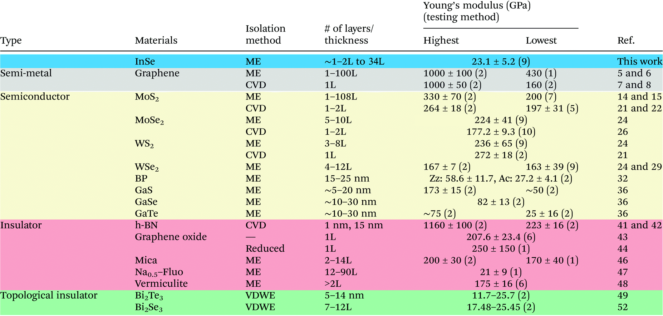
Two-dimensional (2D) semiconductors have attracted a great deal of interest from the scientific community due to their interesting electrical and optical properties that make them promising candidates for future electronic and optoelectronic applications.1–3 For example, 2D transition metal dichalcogenides (TMDCs) have demonstrated remarkable performances in field-effect transistors (FETs), photodetectors, solar cells, and logic circuits.4 Another interesting feature of 2D semiconductors is that they can sustain very large deformations without breaking. This has motivated the application of 2D semiconductors in flexible electronic devices and strain engineering studies.9–12 The flexible electronic devices based on 2-dimensional semiconductors stand out due to their high carrier transport mobility, high specific surface area, high optical transparency, excellent mechanical resilience, and environmental stability.13 Also, the strain engineering on 2D semiconductors, explored first theoretically and then experimentally,16,17 allows one for the modification of the band gap of these materials by means of mechanical deformations of their lattices.18–20 These desirable features indicate that 2D semiconductors are a very promising alternative to traditional flexible organic semiconducting devices. Nevertheless, most of the 2D semiconductors studied so far are extremely stiff, having a Young's modulus in the range of ∼100–300 GPa (a value much larger than that of organic semiconducting materials (0.1–10 GPa),23 see Table 1 and Fig. 3a). This means that a high stress is required to deform them. Therefore, flexible (or compliant) 2D semiconductors (characterized by a low Young's modulus) would be desirable for certain applications including (1) flexible electronic applications, where a semiconductor material with a low Young's modulus mismatch with the polymeric/foil substrate is required,25 (2) force sensing, (3) strain engineering, in which one wants to avoid slippage during strain cycles,27,28 and (4) nano-electro-mechanical systems, where one wants the resonators to behave in the membrane-like regime.30,31
|
Here, we use the buckling-based metrology method to measure the Young's modulus of thin InSe,24 a promising 2D semiconductor that shows record-high electron mobility and ultrahigh photoresponse.33–35 We determine the Young's modulus value E = 23.1 ± 5.2 GPa and we compare this value with the reported values for the other 2D semiconductors, finding that thin InSe is one order of magnitude more flexible than TMDCs. Our results are relevant for the application of InSe in future flexible electronics, straintronic devices, and nanomechanical systems.
Results and discussion
2D thin InSe flakes were isolated by mechanical exfoliation from high quality single crystalline InSe ingots grown by the Bridgman method.37 Bulk InSe have been characterized by scanning electron microscopy (SEM), X-ray diffraction (XRD) and transmission electronic microscopy (TEM) to ensure its high crystallinity and to identify its polytope. More details about the characterization can be found in section 1 of the ESI.† We address the reader to the Materials and methods section for details about the InSe exfoliation. In order to measure the mechanical properties of InSe flakes through the buckling metrology method, they have to be deposited onto a very compliant substrate and subjected to uniaxial compression. In the case of InSe deposited on top of Gel-Film (by Gel-Pak®), if the compression strain in the InSe is above a critical value of approximately 0.07%, the flakes undertake a buckling instability.38 Due to the competition between the buckling of the flakes and the adhesion with the substrate, a wavy pattern (ripples) appears on the flakes. Interestingly, the period of these ripples (λ) depends only on the mechanical properties of the flake and substrate:38–40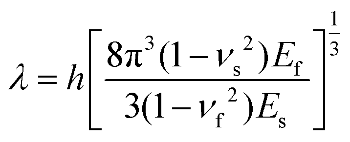 | (1) |
Fig. 1a shows a cartoon of the fabrication process followed to apply the uniaxial compression to InSe flakes. A rectangular shape Gel-Film substrate is slightly bent to induce a uniaxial expansion of its topmost surface. Then InSe flakes are transferred on the bent surface by mechanical exfoliation with Nitto tape (see Materials and methods) and the substrate stress is released yielding the desired uniaxial compression. Fig. 1b shows a transmission mode optical microscopy image of an isolated InSe flake fabricated following this approach. The flake presents a marked wavy pattern because of the buckling instability induced ripples. The corresponding atomic force microscopy (AFM) topography image is shown in Fig. 1b with the thickness ranging from ∼6L to ∼24L (9.4 nm and 24 nm thick). The height calculated from the AFM dynamic mode measurements presented in this work has a systematic offset that we determined to be 4.9 ± 0.5 nm in the case of InSe (this value should be subtracted from the AFM data in order to find the real flake thickness, see section 2 of the ESI†). This offset, which has been reported also for other 2D materials, is caused by the different interaction between the tip and either the substrate or the flake.45 It is important to note that this offset does not influence the determination of the Young's modulus of InSe and thus we did not subtract it from the data presented in this article. Fig. 1c shows the sinusoidal line profile shape of the ripples. From Fig. 1b and c, one can see that the wavelength λ of the ripples is strongly thickness dependent.
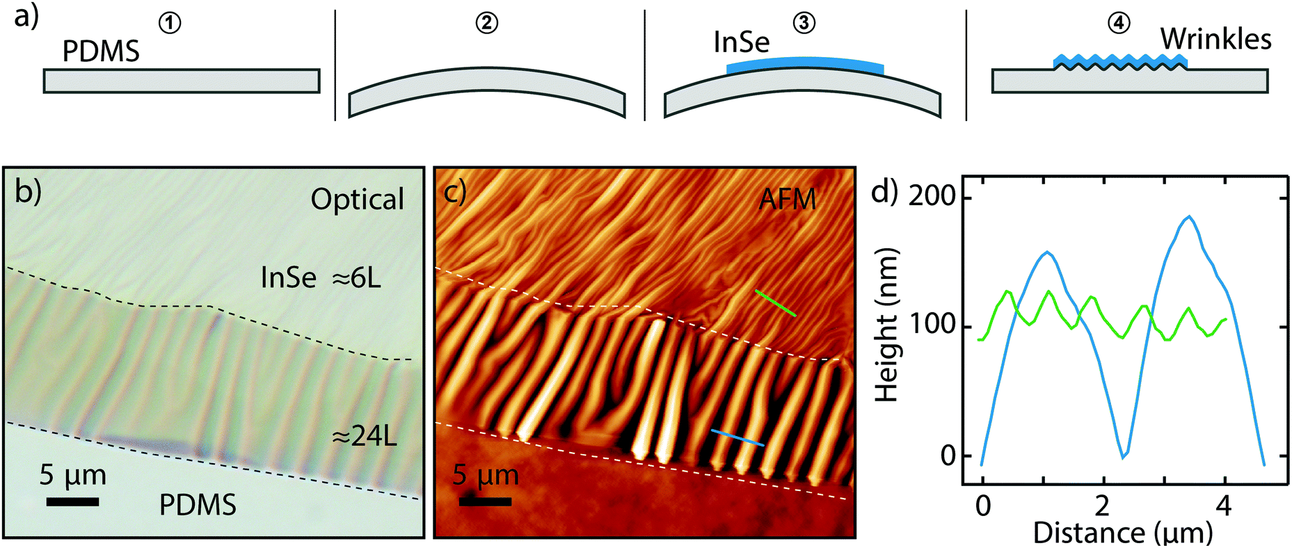 | ||
| Fig. 1 The wrinkled thin InSe flakes. (a) The schematic diagram of fabricating wrinkled InSe flakes on the Gel-Film substrate by using the buckling metrology method. (b, c) Transmission mode optical pictures (b) and surface morphology recorded by AFM (c) of a wrinkled InSe flake with thicknesses (h) of ∼6L and ∼24L. (d) The line profiles of the wrinkles with different thicknesses recorded at the positions marked in panel c (green line, 6L; blue line, 24L). | ||
As seen in eqn (1), the Young's modulus can be determined by measuring the wavelength of the buckling induced ripples for flakes of different thicknesses. Fig. 2a shows six grayscale transmission mode optical images of the ripples produced on InSe flakes with different thicknesses. The wavelength of the ripples can be accurately measured through the fast Fourier transform (FFT) of these images (Fig. 2b). Fig. 2c shows a summary of the wavelength values measured from 20 InSe flakes with thicknesses ranging from 6.4 nm to 32 nm (∼1–2 layers to 34 layers). Note that rippled patterns with wavelengths smaller than ∼1 μm and amplitude < 10 nm cannot be well-resolved with optical microscopy.24 The experimental data points follow a marked linear trend, as expected from eqn (1). From the slope λ/h = 146 ± 11 we can determine the Young's modulus of InSe. Using the known values of the Poisson's ratio of PDMS (Gel-Film) νs = 0.5 and InSe flake νf = 0.27,50,51 and the measured Young's modulus of our Gel-Film Es = 492 ± 11 kPa (see the ESI of ref. 24),24 we determine the Young's modulus of thin InSe flakes, E = 23.1 ± 5.2 GPa, a value much smaller than the reported Young's modulus of other 2D materials.
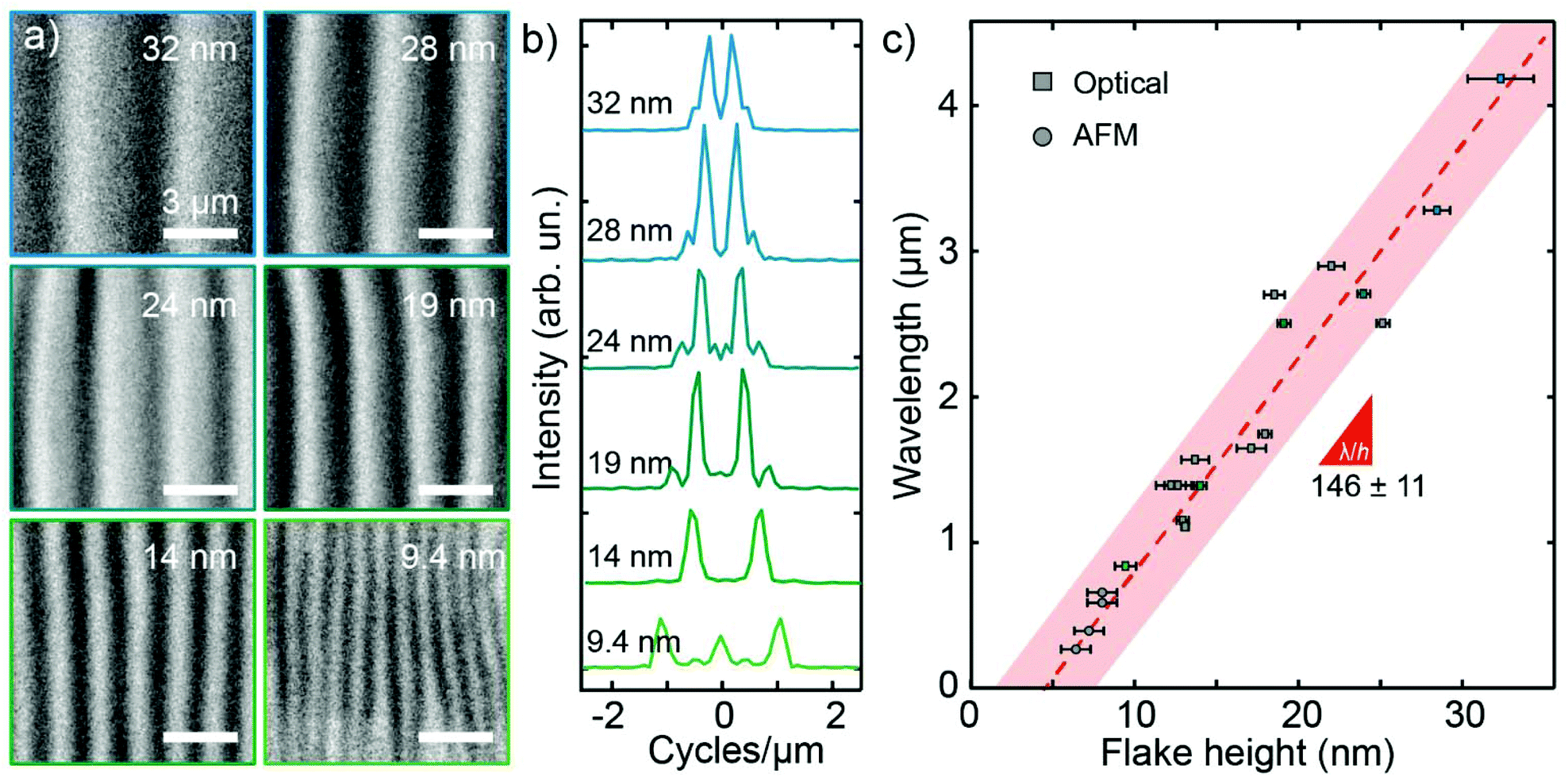 | ||
| Fig. 2 The determination of Young's modulus of thin InSe flakes. (a) Grayscale transmission mode optical microscopy images of wrinkled patterns on InSe flakes with thicknesses ranging from 9.4 nm to 32 nm. (b) The line cuts along the FFT maxima extracted from the optical images in panel a. (c) Relationship between the wavelength of the wrinkles and the thickness of the InSe flakes. The red dashed line represents the linear fit based on the data and the light red shaded area indicates the uncertainty of the fitting. | ||
In order to put this value in the more general context of 2D materials, we show in Fig. 3a a graphical comparison between the Young's modulus values for various isolated 2D materials available in the literature in a semi-logarithm scale plot. We indicate the highest and lowest Young's modulus reported in the literature through the error bar. The four differently colored regions correspond to semimetal, semiconductor, insulator and topological insulator groups, respectively. The value determined with the buckling method of thin InSe Young's modulus is shown with a black dashed line and a surrounding blue shadow (that represents the uncertainty of our measurement result). According to the plot, the thin InSe flakes have a Young's modulus value which is around two orders of magnitude smaller than that of graphene and one order of magnitude lower than MoS2 flakes. This value of the Young's modulus is among the lowest values reported for 2D materials to date and is comparable only to that of metal–organic frameworks (MOFs, ∼5 GPa).53 Notably, this small value for the Young's modulus of InSe is in agreement with theoretical calculations, which predict an isotropic Young's modulus for monolayer InSe of 57 GPa and that this value is much smaller than the predicted values for MoS2 and graphene.50 All the details displayed in Fig. 3a are also summarized in Table 1 to facilitate a quantitative comparison between different materials.
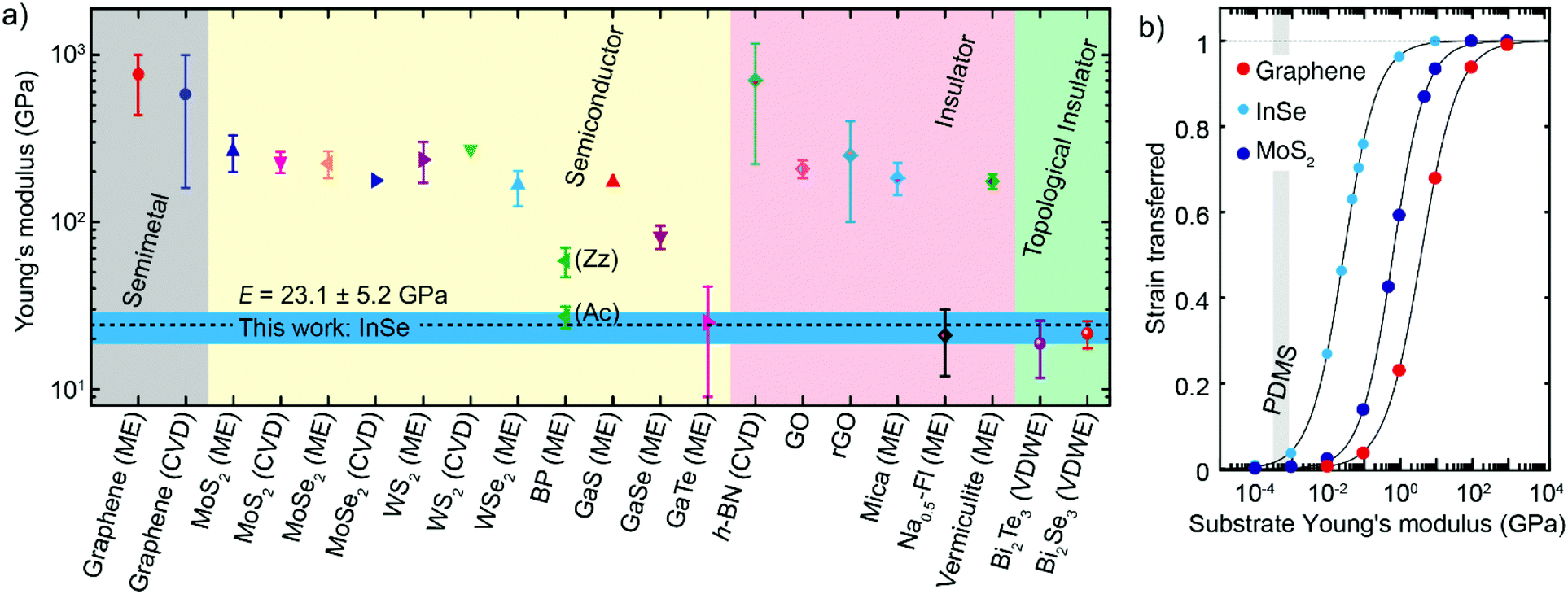 | ||
| Fig. 3 Summary of the experimentally measured Young's modulus values of isolated two-dimensional species (semimetals, semiconductors, insulators and topological insulators). (a) The different values of the Young's modulus of 2D materials reported in the literature are compared with the value of InSe obtained in this work E = 23.1 ± 5.2 GPa (centered at the black dashed line with the blue shaded area indicating the experimental uncertainty). (b) Strain transfer as a function of the substrate Young's modulus calculated from finite element analysis for InSe, MoS2 and graphene. The grey shaded regions indicate the Young's modulus values of polymer substrates typically used in flexible and printed electronics. | ||
The low Young's modulus value of InSe has implications in its applicability in flexible electronics, strain engineering or sensors. For example, applying or transferring strain to a 2D material with a low Young's modulus requires less force than transferring the same amount of strain to a stiffer 2D material. To understand the role of the Young's modulus in the transfer of strain to a 2D material deposited on a substrate, we performed a three-dimensional axisymmetric finite element analysis (FEA) using the software COMSOL Multiphysics (version 5.1). The results shown in Fig. 3b are calculated for a thin InSe with a thickness of 10 nm, a diameter of 20 μm and the Young's modulus EInSe = 23.1 GPa, placed on a substrate with a thickness of 1000 μm and a diameter of 10![[thin space (1/6-em)]](https://www.rsc.org/images/entities/char_2009.gif) 000 μm. Additional details about the FEA calculation can be found in section 3 of the ESI.† The interface between the InSe flake and the substrate is modeled using perfect bonding. In each step of the simulation we allowed the substrate to expand and extracted the total expansion induced in the InSe flake from which we calculated the strain transfer for all the different substrate Young's modulus values. We repeated the calculation for MoS2 (EMoS2 = 250 GPa) and graphene (EGraphene = 1 TPa).5,7,24 The calculations show that, independently of the Young's modulus of the 2D material, for very small values of the substrate Young's modulus no strain is transferred from the substrate to the 2D flake, while for very large values the strain transfer approaches 100%. In between these two limits one can see that the strain transfer presents in all three cases a similar sigmoidal shape and is shifted along the horizontal axis. The onset of transfer of each curve depends on the 2D material Young's modulus being the lowest for InSe and the largest for graphene. For 2D flakes with a lower Young's modulus the strain transfer is larger than for flakes with a larger modulus (given the same substrate Young's modulus). Since no atomistic details are taken into account in the simulation, the real absolute value of strain transfer for a given substrate's Young's modulus can differ from the calculated one. Nevertheless, the general shape of the strain transfer curve and the trend observed should hold true for all the different 2D materials.
000 μm. Additional details about the FEA calculation can be found in section 3 of the ESI.† The interface between the InSe flake and the substrate is modeled using perfect bonding. In each step of the simulation we allowed the substrate to expand and extracted the total expansion induced in the InSe flake from which we calculated the strain transfer for all the different substrate Young's modulus values. We repeated the calculation for MoS2 (EMoS2 = 250 GPa) and graphene (EGraphene = 1 TPa).5,7,24 The calculations show that, independently of the Young's modulus of the 2D material, for very small values of the substrate Young's modulus no strain is transferred from the substrate to the 2D flake, while for very large values the strain transfer approaches 100%. In between these two limits one can see that the strain transfer presents in all three cases a similar sigmoidal shape and is shifted along the horizontal axis. The onset of transfer of each curve depends on the 2D material Young's modulus being the lowest for InSe and the largest for graphene. For 2D flakes with a lower Young's modulus the strain transfer is larger than for flakes with a larger modulus (given the same substrate Young's modulus). Since no atomistic details are taken into account in the simulation, the real absolute value of strain transfer for a given substrate's Young's modulus can differ from the calculated one. Nevertheless, the general shape of the strain transfer curve and the trend observed should hold true for all the different 2D materials.
Conclusions
In conclusion, we reported the experimental value of the Young's modulus of thin InSe flakes using the buckling metrology method. We find an ultralow value in the range of 18–28 GPa, which makes thin InSe one of the most flexible two-dimensional materials. This low Young's modulus value can prove to be highly valuable in applications such as force sensing (as the same force will produce a larger deformation in InSe than in other 2D semiconductors) or flexible electronic applications (where a small mismatch between the Young's modulus of the substrate and the 2D semiconductor is required to avoid stress accumulation after several flexing cycles). Also, we calculate that such superior flexibility may facilitate more effective strain transfer from a polymeric substrate to InSe flakes deposited on top, making InSe a very interesting material for applications in future straintronic devices.Materials and methods
Materials and sample fabrication
The high-quality InSe crystal was grown by the Bridgman method. With the atomic ratio In:Se = 52:48, high purity indium (99.9999%) and selenium (99.9999%) elements are sealed into a quartz crucible under the high vacuum conditions (2 × 10⁻⁵ Pa). Then the quartz crucible was transferred into a rocking furnace and kept swinging for 48 h at 650 °C to mix the melt completely. Then a vertical Bridgman furnace with a temperature gradient of 10 °C cm−1 was used for crystal growth. Detailed characterization of the high-quality bulk materials can be found in section 1 of the ESI.† The elastomeric compliant substrate used in this work is commercially available polydimethylsiloxane (PDMS) supplied by Gel-Pak (WF 4x Gel-Film), whose Young's modulus (Es = 492 ± 11 kPa) has been determined in our previous work.24 A mechanical exfoliation method with Scotch tape (3M®) and Nitto tape (Nitto Denko® SPV 224) was used for thin InSe flake fabrication. Then the flakes were transferred onto a curved Gel-Film substrate to induce wrinkles. All the exfoliation processes are carried out in an ambient environment and at room temperature.
Determination of wrinkle size and flake thickness
The images of rippled InSe flakes onto PDMS were acquired in optical microscopy transmission mode (Motic® BA310 MET-T) in the case of wrinkles with wavelengths larger than ∼1 μm and with dynamic mode atomic force microscopy in the case of wavelengths smaller than 1 μm. After that, these rippled flakes were transferred onto SiO2 (280 nm)/Si substrates for AFM measurements. Gwyddion software was used for the quantitative analysis of the wavelength of the ripples on the flakes. The thickness of InSe flakes was determined by using an ezAFM from Nanomagnetics operating in dynamic mode. A Tap190Al-G cantilever by BudgetSensors with a force constant of 40 N m−1 and a resonance frequency of 300 kHz was used. To take into account the offset present in the thickness determination of 2D flakes by dynamic mode AFM,45 one has to subtract a constant value of 4.9 nm from the raw AFM heights. See section S2 of the ESI† for more details on the estimation of this offset. Note that all the thickness values given in the main text include this offset and thus to find the real thickness one has to subtract 4.9 nm from the reported height.Conflicts of interest
There are no conflicts to declare.Acknowledgements
This project has received funding from the European Research Council (ERC) under the European Union's Horizon 2020 research and innovation program (grant agreement no. 755655, ERC-StG 2017 project 2D-TOPSENSE). EU Graphene Flagship funding (Grant Graphene Core 2, 785219) is acknowledged. RF acknowledges support from the Spanish Ministry of Economy, Industry and Competitiveness through a Juan de la Cierva-formación fellowship (2017 FJCI-2017-32919). QHZ acknowledges the grant from the China Scholarship Council (CSC) under no. 201700290035. TW acknowledges support from the National Natural Science Foundation of China: 51672216.References
- Q. H. Wang, K. Kalantar-Zadeh, A. Kis, J. N. Coleman and M. S. Strano, Nat. Nanotechnol., 2012, 7, 699–712 CrossRef CAS PubMed.
- K. F. Mak and J. Shan, Nat. Photonics, 2016, 10, 216 CrossRef CAS.
- J. F. Sánchez-Royo, G. Muñoz-Matutano, M. Brotons-Gisbert, J. P. Martínez-Pastor, A. Segura, A. Cantarero, R. Mata, J. Canet-Ferrer, G. Tobias and E. Canadell, Nano Res., 2014, 7, 1556–1568 CrossRef.
- S. Manzeli, D. Ovchinnikov, D. Pasquier, O. V. Yazyev and A. Kis, Nat. Rev. Mater., 2017, 2, 17033 CrossRef CAS.
- C. Lee, X. Wei, J. W. Kysar and J. Hone, science, 2008, 321, 385–388 CrossRef CAS PubMed.
- F. Traversi, F. J. Gúzman-Vázquez, L. G. Rizzi, V. Russo, C. S. Casari, C. Gómez-Navarro and R. Sordan, New J. Phys., 2010, 12, 023034 CrossRef.
- G.-H. Lee, R. C. Cooper, S. J. An, S. Lee, A. Van Der Zande, N. Petrone, A. G. Hammerberg, C. Lee, B. Crawford and W. Oliver, Science, 2013, 340, 1073–1076 CrossRef CAS PubMed.
- C. S. Ruiz-Vargas, H. L. Zhuang, P. Y. Huang, A. M. Van Der Zande, S. Garg, P. L. McEuen, D. A. Muller, R. G. Hennig and J. Park, Nano Lett., 2011, 11, 2259–2263 CrossRef CAS PubMed.
- R. Roldán, A. Castellanos-Gomez, E. Cappelluti and F. Guinea, J. Phys.: Condens. Matter, 2015, 27, 313201 CrossRef PubMed.
- D. Akinwande, N. Petrone and J. Hone, Nat. Commun., 2014, 5, 5678 CrossRef CAS PubMed.
- S. Deng, A. V. Sumant and V. Berry, Nano Today, 2018, 22, 14–35 CrossRef CAS.
- Z. Dai, L. Liu and Z. Zhang, Adv. Mater., 2019, 1805417 CrossRef PubMed.
- S. J. Kim, K. Choi, B. Lee, Y. Kim and B. H. Hong, Annu. Rev. Mater. Res., 2015, 45, 63–84 CrossRef CAS.
- A. Castellanos-Gomez, M. Poot, G. A. Steele, H. S. van der Zant, N. Agraït and G. Rubio-Bollinger, Adv. Mater., 2012, 24, 772–775 CrossRef CAS PubMed.
- J. Lee, Z. Wang, K. He, J. Shan and P. X.-L. Feng, ACS Nano, 2013, 7, 6086–6091 CrossRef CAS PubMed.
- J. Feng, X. Qian, C.-W. Huang and J. Li, Nat. Photonics, 2012, 6, 866 CrossRef CAS.
- H. Li, A. W. Contryman, X. Qian, S. M. Ardakani, Y. Gong, X. Wang, J. M. Weisse, C. H. Lee, J. Zhao and P. M. Ajayan, Nat. Commun., 2015, 6, 7381 CrossRef CAS PubMed.
- M. Brotons-Gisbert, D. Andres-Penares, J. Suh, F. Hidalgo, R. Abargues, P. J. Rodríguez-Cantó, A. Segura, A. Cros, G. Tobias and E. Canadell, Nano Lett., 2016, 16, 3221–3229 CrossRef CAS PubMed.
- Y. Li, T. Wang, H. Wang, Z. Li, Y. Chen, D. West, R. Sankar, R. K. Ulaganathan, F. Chou and C. Wetzel, Nano Lett., 2018, 18, 5078–5084 CrossRef CAS PubMed.
- Y. Li, T. Wang, M. Wu, T. Cao, Y. Chen, R. Sankar, R. K. Ulaganathan, F. Chou, C. Wetzel and C.-Y. Xu, 2D Mater., 2018, 5, 021002 CrossRef.
- K. Liu, Q. Yan, M. Chen, W. Fan, Y. Sun, J. Suh, D. Fu, S. Lee, J. Zhou and S. Tongay, Nano Lett., 2014, 14, 5097–5103 CrossRef CAS PubMed.
- D. Lloyd, X. Liu, N. Boddeti, L. Cantley, R. Long, M. L. Dunn and J. S. Bunch, Nano Lett., 2017, 17, 5329–5334 CrossRef CAS PubMed.
- B. H. Stuart, Polymer analysis, John Wiley & Sons, 2008 Search PubMed.
- N. Iguiñiz, R. Frisenda, R. Bratschitsch and A. Castellanos-Gomez, Adv. Mater., 2019, 1807150 CrossRef PubMed.
- H. Gleskova, I.-C. Cheng, S. Wagner, J. C. Sturm and Z. Suo, Sol. Energy, 2006, 80, 687–693 CrossRef CAS.
- Y. Yang, X. Li, M. Wen, E. Hacopian, W. Chen, Y. Gong, J. Zhang, B. Li, W. Zhou and P. M. Ajayan, Adv. Mater., 2017, 29, 1604201 CrossRef PubMed.
- R. Frisenda, M. Drüppel, R. Schmidt, S. M. de Vasconcellos, D. P. de Lara, R. Bratschitsch, M. Rohlfing and A. Castellanos-Gomez, npj 2D Mater. Appl., 2017, 1, 10 CrossRef.
- C. Rice, R. Young, R. Zan, U. Bangert, D. Wolverson, T. Georgiou, R. Jalil and K. Novoselov, Phys. Rev. B: Condens. Matter Mater. Phys., 2013, 87, 081307 CrossRef.
- R. Zhang, V. Koutsos and R. Cheung, Appl. Phys. Lett., 2016, 108, 042104 CrossRef.
- A. Castellanos-Gomez, R. van Leeuwen, M. Buscema, H. S. van der Zant, G. A. Steele and W. J. Venstra, Adv. Mater., 2013, 25, 6719–6723 CrossRef CAS PubMed.
- A. Castellanos-Gomez, V. Singh, H. S. van der Zant and G. A. Steele, Ann. Phys., 2015, 527, 27–44 CrossRef CAS.
- J. Tao, W. Shen, S. Wu, L. Liu, Z. Feng, C. Wang, C. Hu, P. Yao, H. Zhang and W. Pang, ACS Nano, 2015, 9, 11362–11370 CrossRef CAS PubMed.
- D. A. Bandurin, A. V. Tyurnina, L. Y. Geliang, A. Mishchenko, V. Zólyomi, S. V. Morozov, R. K. Kumar, R. V. Gorbachev, Z. R. Kudrynskyi and S. Pezzini, Nat. Nanotechnol., 2017, 12, 223 CrossRef CAS PubMed.
- S. A. Wells, A. Henning, J. T. Gish, V. K. Sangwan, L. J. Lauhon and M. C. Hersam, Nano Lett., 2018, 18, 7876–7882 CrossRef CAS PubMed.
- M. Li, C. Y. Lin, S. H. Yang, Y. M. Chang, J. K. Chang, F. S. Yang, C. Zhong, W. B. Jian, C. H. Lien and C. H. Ho, Adv. Mater., 2018, 1803690 CrossRef PubMed.
- B. Chitara and A. Ya'akobovitz, Nanoscale, 2018, 10, 13022–13027 RSC.
- T. Ishii, J. Cryst. Growth, 1988, 89, 459–462 CrossRef CAS.
- D. Y. Khang, J. A. Rogers and H. H. Lee, Adv. Funct. Mater., 2009, 19, 1526–1536 CrossRef CAS.
- C. M. Stafford, C. Harrison, K. L. Beers, A. Karim, E. J. Amis, M. R. VanLandingham, H.-C. Kim, W. Volksen, R. D. Miller and E. E. Simonyi, Nat. Mater., 2004, 3, 545 CrossRef CAS PubMed.
- A. Volynskii, S. Bazhenov, O. Lebedeva and N. Bakeev, J. Mater. Sci., 2000, 35, 547–554 CrossRef CAS.
- S. M. Kim, A. Hsu, M. H. Park, S. H. Chae, S. J. Yun, J. S. Lee, D.-H. Cho, W. Fang, C. Lee and T. Palacios, Nat. Commun., 2015, 6, 8662 CrossRef CAS PubMed.
- L. Song, L. Ci, H. Lu, P. B. Sorokin, C. Jin, J. Ni, A. G. Kvashnin, D. G. Kvashnin, J. Lou and B. I. Yakobson, Nano Lett., 2010, 10, 3209–3215 CrossRef CAS PubMed.
- J. W. Suk, R. D. Piner, J. An and R. S. Ruoff, ACS Nano, 2010, 4, 6557–6564 CrossRef CAS PubMed.
- C. Gómez-Navarro, M. Burghard and K. Kern, Nano Lett., 2008, 8, 2045–2049 CrossRef PubMed.
- P. Nemes-Incze, Z. Osváth, K. Kamarás and L. Biró, Carbon, 2008, 46, 1435–1442 CrossRef CAS.
- A. Castellanos-Gomez, M. Poot, A. Amor-Amorós, G. A. Steele, H. S. van der Zant, N. Agraït and G. Rubio-Bollinger, Nano Res., 2012, 5, 550–557 CrossRef CAS.
- D. A. Kunz, E. Max, R. Weinkamer, T. Lunkenbein, J. Breu and A. Fery, Small, 2009, 5, 1816–1820 CrossRef CAS PubMed.
- J. W. Suk, R. D. Piner, J. An and R. S. Ruoff, Thin Solid Films, 2013, 527, 205–209 CrossRef CAS.
- L. Guo, H. Yan, Q. Moore, M. Buettner, J. Song, L. Li, P. T. Araujo and H.-T. Wang, Nanoscale, 2015, 7, 11915–11921 RSC.
- T. Hu, J. Zhou and J. Dong, Phys. Chem. Chem. Phys., 2017, 19, 21722–21728 RSC.
- R. H. Pritchard, P. Lava, D. Debruyne and E. M. Terentjev, Soft Matter, 2013, 9, 6037–6045 RSC.
- H. Yan, C. Vajner, M. Kuhlman, L. Guo, L. Li, P. T. Araujo and H.-T. Wang, Appl. Phys. Lett., 2016, 109, 032103 CrossRef.
- C. Hermosa, B. R. Horrocks, J. I. Martínez, F. Liscio, J. Gómez-Herrero and F. Zamora, Chem. Sci., 2015, 6, 2553–2558 RSC.
Footnote |
| † Electronic supplementary information (ESI) available: Characterization of bulk InSe (SEM, EDX, XRD and TEM), details on the AFM thickness determination and on the finite element analysis simulation. See DOI: 10.1039/c9nr02172h |
| This journal is © The Royal Society of Chemistry 2019 |