
 Open Access Article
 This Open Access Article is licensed under a Creative Commons Attribution-Non Commercial 3.0 Unported Licence
Epitaxial multilayers of alkanes on two-dimensional black phosphorus as passivating and electrically insulating nanostructures†
Margherita
Bolognesi
 a,
Marco
Brucale
*a,
Andrea
Lorenzoni
a,
Federico
Prescimone
a,
Salvatore
Moschetto
a,
Vladimir V.
Korolkov
b,
Matteo
Baldoni
a,
Manuel
Serrano-Ruiz
c,
Maria
Caporali
c,
Francesco
Mercuri
a,
Elena
Besley
d,
Michele
Muccini
a,
Maurizio
Peruzzini
c,
Peter H.
Beton
b and
Stefano
Toffanin
*a
a,
Marco
Brucale
*a,
Andrea
Lorenzoni
a,
Federico
Prescimone
a,
Salvatore
Moschetto
a,
Vladimir V.
Korolkov
b,
Matteo
Baldoni
a,
Manuel
Serrano-Ruiz
c,
Maria
Caporali
c,
Francesco
Mercuri
a,
Elena
Besley
d,
Michele
Muccini
a,
Maurizio
Peruzzini
c,
Peter H.
Beton
b and
Stefano
Toffanin
*a
aIstituto per lo Studio dei Materiali Nanostrutturati (ISMN) - Consiglio Nazionale delle Ricerche (CNR), Via P. Gobetti 101, 40129 Bologna, Italy. E-mail: m.brucale@bo.ismn.cnr.it; s.toffanin@bo.ismn.cnr.it
bSchool of Physics and Astronomy, University of Nottingham, Nottingham NG7 2RD, UK
cIstituto di Chimica dei Composti Organometallici (ICCOM) - Consiglio Nazionale delle Ricerche (CNR), Via Madonna del Piano 10, 50019 Sesto Fiorentino, Florence, Italy
dSchool of Chemistry, University of Nottingham, Nottingham NG7 2RD, UK
First published on 18th July 2019
Abstract
Mechanically exfoliated two-dimensional (2D) black phosphorus (bP) is epitaxially terminated by monolayers and multilayers of tetracosane, a linear alkane, to form a weakly interacting van der Waals heterostructure. Atomic force microscopy (AFM) and computational modelling show that epitaxial domains of alkane chains are ordered in parallel lamellae along the principal crystalline axis of bP, and this order is extended over a few layers above the interface. Epitaxial alkane multilayers delay the oxidation of 2D bP in air by 18 hours, in comparison to 1 hour for bare 2D bP, and act as an electrical insulator, as demonstrated using electrostatic force microscopy. The presented heterostructure is a technologically relevant insulator-semiconductor model system that can open the way to the use of 2D bP in micro- and nanoelectronic, optoelectronic and photonic applications.
Introduction
Few-layer black phosphorus (FL-bP) and single-layer black phosphorus (phosphorene), often jointly referred to as 2D bP, are currently regarded as one of the most promising emerging 2D materials. Unlike zero-gap graphene, 2D bP is a semiconductor, with a thickness-dependent band gap,1 ranging from 2 eV (phosphorene)2 to 0.3 eV (bulk bP).3 These characteristics set this material apart from e.g. transition metal dichalcogenides (TMDs), which show direct band gaps in their monolayer form. Over the last five years, both the fundamental physics and applied material science communities have devoted substantial research efforts to 2D bP. This work has encompassed both an understanding of physics behind the peculiar characteristics of bP in the 2D regime (e.g. its tunable bandgap and its anisotropic opto-electrical behavior) and fabrication and optimization of efficient 2D bP-based optoelectronic micro-devices.4 Field effect transistors fabricated from exfoliated bP have been reported, and show very high carrier mobility (up to 6500 cm2 V−1 s−1)5 and high speed (cutoff frequency of 12 GHz),6 together with photodiode-like UV-vis-IR photodetectors with high sensitivity (UV photoresponsivity of ∼105 A W−1),7 and on/off ratios (105).8While 2D bP shares some structural similarities with other 2D materials, it is more reactive, but it is nevertheless possible to fabricate novel 2D micro-optoelectronic components and devices including photodetectors, solar cells, light-emitting devices, photonic crystals and switchable optical components, which have evolved rapidly in recent years.9
One major drawback of the high surface reactivity of bP is that it rapidly oxidizes under atmospheric conditions.10 The most widely adopted approach used to overcome this issue relies on the deposition of thick inert protecting films, such as poly(methyl methacrylate) (PMMA) or Al2O3.11 Some recent literature reports also on nanocomposites of 2D bP, with the same PMMA or polyaniline, for stabilization purposes. In this approach, 2D bP flakes are either directly blended with the polymer in solution, or 2D bP flakes are formed by liquid phase exfoliation of bP in presence of monomeric precursors, which are then allowed to polymerize.12 Alternatively, molecular nanolayers in lieu of thicker protective layers have been reported more recently.13 In addition, bP may be embedded in van der Waals (vdW) heterostructures.14 Heterostructures based on 2D bP and transition metal dichalcogenides, graphene, or mixed metal oxides have indeed shown a good stability towards oxidation, accompanied by an excellent functionality as optoelectronic devices,15 high-capacity anodes for sodium-ion batteries,16 and as new artificial photocatalytic systems for water splitting.17 However, such 2D bP-based heterostructures are often prepared through atomic layer deposition techniques or they require a mechanical alignment between two layers, which is time-consuming and unwieldy process. Epitaxial monolayers of organic molecules can be formed more easily on 2D bP via solution deposition or high vacuum sublimation techniques.18 The relevant literature reports a single example of 2D bP covalent functionalization,19 and most other studies rely only on non-covalently interacting epitaxial monolayers on 2D bP.20
In this context, the choice of organic molecules, which are completely inert and only weakly interact with 2D bP through vdW forces, appears promising. Since a full coverage is necessary for protection purposes, this approach would be particularly suitable for single layer phosphorene as its electronic structure is not expected to be modified by a weakly interacting epitaxial monolayer and thus its unique physical and chemical properties would be preserved. In addition, the semiconducting 2D bP/insulator heterostructure could be introduced and characterized in metal–insulator-semiconductor (MIS) devices, as it has already been done in organic electronics.21 Unlike conjugated organic compounds,22 linear akanes are relatively inert and they have insulating characteristics. They are also inexpensive and readily available materials. Finally, when these molecules are physisorbed on graphene,23 metallic gold,24 or other flat surfaces,25 they form ordered 2D crystalline structures, stabilized by noncovalent in-plane interactions, which can be accurately mapped by scanning probe techniques.23–26
Motivated by these observations, we study the morphological and electrical characteristics and the stability in air of a vdW epitaxial system composed of 2D bP coated with alkane nano-layers, as a technologically relevant model system for applications in 2D micro-electronics and photonics. Among n-alkanes, tetracosane (a linear alkane with 24 C atoms, named as C24 herein) was selected due to its low molecular weight which results in: (i) easy solubility in standard organic solvents; (ii) easy visualization of molecular-scale features using atomic force microscopy (AFM); (iii) a high lateral mobility on the bP surface to allow for self-ordering upon mild thermal treatments; (iv) a melting point (∼50 °C) above room temperature and a low vapor pressure.27 A monolayer of C24 on a bulk bP crystal was employed as a model system to investigate surface coverage and epitaxial ordering. Once functionalized with epitaxially ordered multilayers of C24, the system composed of exfoliated 2D bP deposited onto a technologically relevant substrate has been characterized to determine its stability and the electrostatic properties in ambient conditions. Finally, computational modeling has provided a deeper understanding, at the molecular level, of the energetics, dynamics and structural ordering within the layers of the system.
Experimental section
Materials and methods
Computational studies
Simulations of the aggregation of alkanes at the interface with bP were performed by molecular dynamics (MD) and density functional theory (DFT). bP was modelled using the interatomic potential described in the work of Sresht et al.,30 while standard Optimized Potential for Liquid Simulations (OPLS) parameters were adopted for C24 molecules.31 MD simulations were carried out using the LAMMPS package.32 The aggregation of alkanes on bP was investigated by applying a combination of non-equilibrium and equilibrium MD, based on a protocol previously developed for a different system.33 A 5-layer slab of bP, with lateral size of about 10 × 10 nm, was initially equilibrated at room temperature. Initial amorphous aggregates of C24 molecules at the interface with the bP were obtained by progressively adding C24 chains to the simulation box. Molecules were inserted in the box at a distance of 4 nm from the surface, with random initial positions on the xy plane and a velocity along the z direction of 0.5 nm ps−1. Individual C24 molecules were added to the system every 25 ps, until 100 molecules were inserted. The system was then equilibrated for 20 ns at 300 K. The C24 aggregates were subsequently analysed by evaluating the orientation angle φ, defined as the angle between the long axis of each alkane molecule and the lattice vector e1 (zig-zag direction, defined in the main text) of bP; the values of φ angle were sampled every 100 ps for the last 5 ns of the simulation.In a different set of MD simulations, the energetics and dynamics of a small planar aggregate of C24 molecules on bP has been assessed. Ten C24 molecules were aligned to form a morphology compatible with the in-plane structure of C24 crystals24 and optimized in vacuum. The optimized layer of C24 molecules was then placed above the bP surface in different orientations and the system was equilibrated at 300 K for 5 ns (see ESI† for further details). The effect of temperature on the morphology of C24 aggregates on bP was studied by annealing the equilibrated systems at higher temperatures. Namely, the system was annealed at 320 K at a rate of 0.1 K ps−1, equilibrated at 320 K for 5 ns, cooled to 300 K at a rate of 0.025 K ps−1 and equilibrated at 300 K for 5 ns.
To validate the results obtained with classical MD, a series of DFT calculation have been performed on smaller systems. A phosphorene sheet of about 5 × 5 nm was optimized in vacuum, and a single chain of C24 was positioned on top of the phosphorene surface at different initial orientations: 0°, 25°, 55°, 75° and 90° with respect to the e1 direction of bP. The alkane structure was then optimized keeping the atomic positions of phosphorene frozen. These calculations have been repeated for an array of four parallel alkane chains to assess the influence of the cooperative behavior of multiple chains. The adsorption energy was estimated as [E(C24@Phosphorene) − nE(C24) − E(Phosphorene)]/n, where n is the number of chains in the aggregate. Further details on these simulations can be found in the ESI.†
Results and discussion
Oxidation behavior of pristine 2D bP flakes
As previously reported, pristine 2D bP flakes are extremely prone to oxidation when exposed to humid air.34 After exfoliation, their surface is atomically flat (Sq = 0.3 ± 0.1 nm) with occasional monoatomic steps (see Fig. 1a). Within a few minutes of exposure to air, raised “bubble-like” regions begin to appear, until after 1 hour of exposure the majority of the surface is affected (bringing average Sq to 2.7 ± 0.5 nm, Fig. 1b). As reported in the literature, their formation is due to the evolution of POx species during oxidation.35 The oxidized zones give rise to an appreciable contrast in the Peak Force Tapping quadrature AFM signal (see Fig. 1b), suggesting that the structures have different mechanical characteristics compared to pristine bP surface. | ||
| Fig. 1 Representative AFM topography and peakforce quadrature (inset) of a pristine 2D bP flake immediately after exfoliation (a) and after being exposed to humid air for 60 min (b). All images are 1 × 1 μm. | ||
Epitaxial ordering of a C24 monolayer on bulk bP
In order to determine the molecular ordering and orientation relative to the bP crystal lattice we first consider a C24 monolayer deposited on the surface of a bP crystal. Tapping mode AFM images are presented in Fig. 2 together with a schematic molecular model.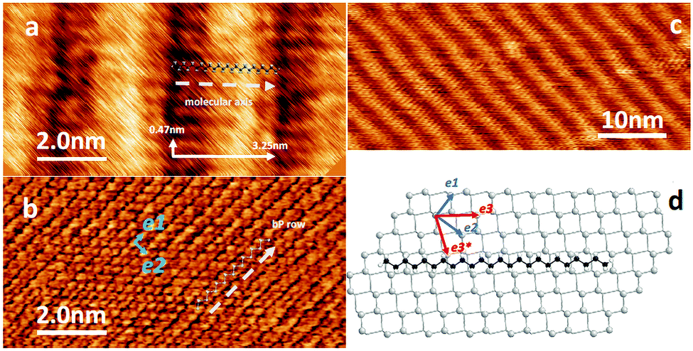 | ||
| Fig. 2 (a) and (c) AFM tapping mode images of a C24 monolayer arranged on the surface of a bulk bP crystal. (a) Lamellar rows separated by 3.25 nm and intermolecular spacing within the row of 0.47 nm. (b) AFM tapping mode scan of the bP surface after C24 molecules were removed; this corresponds to the same area as imaged in (a) allowing a direct determination of the molecular ordering relative to the substrate – the arrows in (a) and (b) indicate the direction of the, respectively, the molecular axis and the phosphorus rows at the bP surface; (c) larger area image showing the lamellar rows; (d) schematic crystalline structure of the bP surface with an overlaid C24 molecule. Both geometries were extracted from experimental data. e1 and e2 are the lattice vectors of the rectangular bP unit cell; the molecular axis is aligned with e3, a vector along the diagonal of the rectangular surface unit cell. e3* is a symmetry equivalent direction. | ||
High-resolution AFM images (Fig. 2a) reveal a typical lamellar arrangement of the C24 molecules (shown over larger areas in Fig. 2c) with a measured row spacing of 3.25 ± 0.06 nm and a periodicity along the row, corresponding to the intermolecular separation, of 0.47 ± 0.02 nm. These values are in excellent agreement with single crystal X-ray diffraction data of linear C24 (a = 3.254 nm, b = 0.482 nm).36 By progressively increasing the tip–sample force during imaging with AFM in tapping mode, the C24 monolayer can be locally removed. In this way, it is possible to acquire the tapping mode AFM images of the bP surface under the alkane layer (Fig. 2b) and to resolve the top-layer bP atoms, which appear as zigzag rows with a separation of 0.44 ± 0.02 nm. Also, resolved along the rows are periodic topographic features with a spacing of 0.33 ± 0.02 nm. These values match the lattice vectors of the bP surface.20,37 Since these images (Fig. 2a and b) have the same orientation, we can determine that the C24 chains are aligned approximately along the diagonal of the bP rectangular unit cell. The arrangement is shown schematically in Fig. 2d in which the surface phosphorus atoms are shown as shaded circles. In Fig. 2d the lattice vectors e1 and e2 are shown, and the unit cell diagonal is denoted as e3; this direction is at an angle of 53.1° to the e1 lattice vector. There is an equivalent symmetry direction denoted e3*, at an angle of 73.6° to the e3 direction, which is expected to result in a symmetry-equivalent ordering leading to a second domain rotated by this angle. Under the preparation conditions, we do not observe boundaries between differently oriented regions since each domain is large (>1 μm; see Fig. S3 in ESI†). However, as shown below, two differently ordered domains are observed in the multilayer samples.
We have also observed a variation in contrast within a single lamellar row which appears as a 1.65 nm wide topographic feature. This feature is attributed to a variation in the local adsorption site of the CH2-groups within the molecule, i.e. the relative position of these groups to the surface phosphorus atoms. This variation is a consequence of the mismatch between the spacing of the CH2-groups and the position of phosphorus atoms along this crystallographic direction.
The adsorption of C24 molecules on the bP surface was investigated using molecular dynamics (MD) simulations at 300 K (see computational details in the Experimental section), which reveal (Fig. 3a) an aggregation of C24 molecules with a coverage corresponding to approximately 1.5 monolayers relaxed on bP. Alkanes form ordered structures on the surface of bP, as evidenced by the distribution of the φ values (Fig. 3b), which shows broaden maxima at around −55°, 0° and 55°, corresponding to the e1 and e3/e3* directions of bP, in good agreement with experimental findings. In all simulations the C24 chains lay on bP with the carbon zig-zag plane parallel to the surface. For C24 aggregates at the interface with bP, the predicted distribution of orientations indicates the presence of three main energy minima (see Molecular modeling section in ESI†). The measured intermolecular distance between the C24 chains ranged between 0.42 and 0.49 nm, in both the preferential orientations, in good agreement with the experimental data. The occurrence of two preferential orientations for alkanes on bP can be related to a particular patterning of phosphorus atoms exposed on the surface of bP, which interact favorably with the C24 atoms driven by vdW forces. The effect of temperature on the observed morphology was investigated by annealing the planar C24 clusters on bP in the two most favorable configurations (along the e1 and e3 directions), as described in ESI.† The C24 layer aligned along the e1 direction was not significantly affected by thermal annealing.
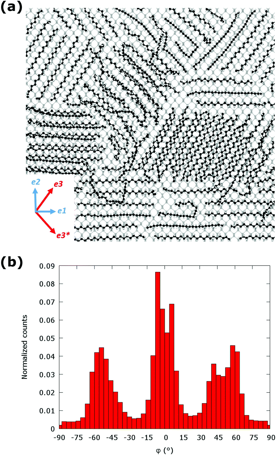 | ||
| Fig. 3 (a) Morphology of aggregates of C24 molecules on the surface of few-layers bP relaxed by MD simulations at 300 K and (b) distribution of the orientation angle φ of the equilibrated system. | ||
Conversely, the C24 layer initially positioned along the e3 direction underwent a dramatic structural relaxation leading to a final equilibrated structure corresponding to φ ≈ 0° (see Fig. S13 in ESI†), thus suggesting that the alignment along the e1 direction is thermodynamically most stable.
The experimental conditions for the deposition of C24 layers at the interface with BP are, however, compatible with the formation of aggregates in both most stable configurations (along the e1 and e3 directions). Indeed, DFT-D3 calculations confirmed that the preferential adsorption orientations are along the e1 and e3 directions, consistent with our MD results. Alignment along the e1 direction is favored with an adsorption energy of −1.78 eV per molecule. The difference between these orientations is comparable to the thermal energy, thus identifying two different minima, both accessible to the aggregate structure, as observed by MD simulations. All other tested orientations of alkane chains on bP surface produced less stable final configurations. The lateral interaction between the alkanes further stabilizes the aggregate of 4 chains by about ≃0.5 eV per chain leaving the overall structural trend essentially unaltered.
Epitaxial ordering and air stability of a C24 monolayer on 2D bP
We next assess the ability of C24 chains to form epitaxially ordered layers on 2D bP and prevent bP oxidation. Pristine 2D bP flakes are expected to be oxidized more quickly than pristine bP crystals.38 Moreover, the difference in the lateral size and thickness between bulk bP crystal and 2D bP flake may also affect the deposition of C24 due to a large amount of defects, reduced planarity and boundary effects in 2D bB flakes. Consequently, functionalized bulk bP and 2D bP flakes may behave differently upon exposure to air. In particular, while micron sized epitaxial domains protect bP over a longer time, as observed on bP crystal, a less regular coverage of a bP flake could be less effective.20 Similarly, a variety in shape, lateral size and thickness of 2D bP flakes produced by mechanical exfoliation could potentially affect both the C24 deposition and the degradation rate of bP surface. Therefore, we perform all measurements on 2D bP flakes with similar thickness (60 ± 10 nm) and lateral size (5–10 μm).In order to reproduce a surface coverage of approximately a monolayer, C24 chains were deposited with the same dip coating technique from a C24 ethanolic solution (see Experimental section). The AFM images (Fig. 4a and b) show a separation of C24 into two phases with different average heights (Fig. S4 in ESI†). While the zones with higher average heights are apparently amorphous, the lower zones show an arrangement of C24 in parallel lamellae. The lateral size of discrete ordered domains is in the range of 100–200 nm (Fig. 4b). These dimensions allow visualization of the same discrete domains containing lamellae aligned along two different epitaxial directions forming an angle of 75 ± 5°. The observed orientations correspond to the alignment of C24 along the e3/e3* directions of the underlying 2D bP surface, in perfect accordance with the AFM measurements of C24 monolayer on bulk bP and with MD simulations. The lamellar average periodicity was estimated to be 3.5 ± 0.2 nm via 2D FFT (Fig. 4a, insets), which is in good agreement with the value measured on bulk bP (see previous section). We have not observed any lamellar structure within the second phase. Hence, we presume it to be amorphous.
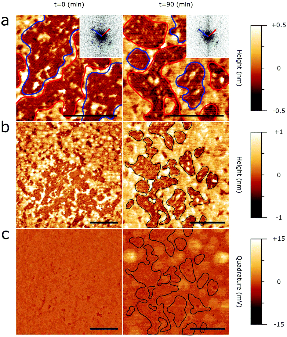 | ||
| Fig. 4 Epitaxial ordering and oxidation inhibition characteristics of a C24 monolayer on 2D bP flakes. (a, b, c): representative morphology (a, b) and PeakForce Tapping quadrature (c) micrographs of a 2D BP flake with a C24 monolayer on top deposited by dip coating (see Materials and methods) immediately after functionalization (left column) or after 90 minutes (right column) of exposition to humid air. All scale bars are 100 nm. (a): Details of the ordered domains with corresponding 2D FFT plots (insets). Solid blue and red lines outline domains showing features aligned in the same general direction, with the corresponding 2D FFT peaks highlighted in the same color. (b): Zoomed-out view of the same zones showing a typical distribution of ordered and disordered domains immediately after deposition (left) or after 90 minutes of air exposure (right; ordered domains are outlined with a solid black line). (c): Quadrature signal of the same areas depicted in panel (b), evidencing the first signs of oxidation damage. The solid black outlines in the right panel correspond to ordered domains identified from the image directly above; these zones appear considerably less subject to oxidation. | ||
To test the protective effect of the C24 monolayer against oxidation of 2D bP, we acquire AFM scans of the same zone of a 2D bP flake functionalized with a C24 monolayer after 90 minutes (Fig. 4, right column) and 240 minutes (Fig. S5 in ESI†) of exposure to air with approximately 50% humidity under standard laboratory illumination (400 lux). While on pristine bP, an evidence of oxidized material begins to emerge after a few minutes and it dominates after 1 hour (Fig. 1), the same process becomes significant only after 90 min on the C24/2D bP surface (Fig. 4c), and it takes 4 hours to reach a qualitatively similar level to that of bulk (Fig. S5 in ESI†). The majority of oxidized zones start to appear in areas covered by amorphous C24 rather than in ordered regions (Fig. 4c). If the force exerted by the AFM tip is increased tenfold from ∼150 pN to ∼1.5 nN (Fig. S5 in ESI†), the oxidation protrusions get leveled down to the same height of the un-oxidized surface, suggesting that they are raised bubbles of delaminated material.
This evidence suggests that ordered C24 layers inhibit the oxidation of 2D bP but the amorphous regions are much less effective. On the whole, this functionalization method allows C24/2D bP heterostructure to remain unperturbed for around 1 hour, instead of a few minutes as pristine 2D bP.
Epitaxial ordering and air stability of C24 multilayers on 2D bP
To improve the protecting properties of epitaxial C24 layers on 2D bP flakes we next used nanometer size multilayers of C24. To this aim, 2D bP flakes on quartz substrates were spun coated with C24 molecules from chloroform solution at varying concentrations and with different post-deposition thermal treatments to optimize coverage and epitaxial ordering.Fig. 5d shows the best combined 2D bP coverage and C24 ordering obtained through successive optimization of deposition protocols (Fig. 5a, b and c). The results range from isolated clusters of lamellae with poor epitaxial ordering in an otherwise bare surface (Fig. 5a), to small ordered domains with abundant (Fig. 5b) or comparatively scarce (Fig. 5c) amounts of amorphous material, to large ordered domains covering most of the 2D bP surface (Fig. 5d). The post-deposition annealing is the most relevant processing parameter. By increasing the annealing temperature from 85 °C to 120 °C and finally to 150 °C, a gradual improvement of the ordering is observed. In detail, the relative coverage with ordered domains passes from 0% of the scanned area (Fig. 5a) to 72–89% (Fig. 5b and c) to 97% (Fig. 5d). Most probably, the increase of temperature favors either the removal of some amorphous material by sublimation, or the amorphous-to-ordered phase change of some C24 domains. As observed in monolayers, C24 chains arrange into ordered domains of parallel lamellae with lateral dimensions ranging from 100–200 nm (Fig. 5b and c) to several microns (Fig. 5d) separated by varying amounts of interstitial amorphous C24. Similar to the results reported in previous section, individual domains show lamellae aligned in two distinct directions forming an angle of 69 ± 5° as measured via 2D FFT plots of AFM topography images (Fig. 5, bottom row). Surprisingly, however, the spacing periodicity between lamellae was found to be different (4.7 ± 0.3 nm) in this case. To elucidate this discrepancy, the thickness of the C24 multilayer was measured by locally removing it with the AFM tip (Fig. S6 in ESI†). Ordered domains were found to be 2 nm thick while the disordered/out-of-plane ones were 3 nm thick. In addition, it is clear in Fig. 5 that some of lamellae are not completely regular and display local bending and splaying. Similar types of disorder and complex arrangements have also been observed in multilayer films of alkanes on hexagonal boron nitride.39 We therefore conclude that the ordered domains deposited in these experimental conditions are composed of several superimposed C24 layers. The reciprocal orientations of lamellae within ordered multilayered domains (two directions at an angle of 69 ± 5°) suggest that the same epitaxial interaction is occurring at the C24/bP interface along the e3/e3* principal axis as in C24 monolayers, and that this order propagates to successive deposited layers. Different structural periodicity of the topmost lamellae suggests that C24 layers do not interact directly with bP and adopt alternative, still poorly understood, arrangements.
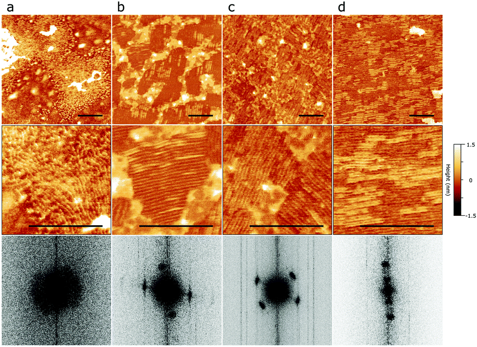 | ||
| Fig. 5 Epitaxial ordering of multilayers of C24 on 2D bP flakes. (a, b, c, d): Representative topography (top, 500 × 500 nm and middle, 150 × 150 nm, scale bar 100 nm) and corresponding 2D FFT plots of 2D BP flakes coated with a C24 chloroform solution following different protocols (see Materials and Methods for details) resulting in the deposition of several layers of C24. Relevant deposition protocol parameters are: (a) 0.01 mg mL−1 C24, thermal annealing at 85 °C for 30 minutes; (b) 0.001 mg mL−1 C24, thermal annealing at 120 °C for 30 minutes; (c) 0.01 mg mL−1 C24, thermal annealing at 120 °C for 30 minutes; (d) C24 0.01 mg mL−1, thermal annealing at 150 °C for 30 minutes. | ||
To investigate the protective effect of C24 multilayers on 2D bP, the AFM scans were acquired of several freshly cleaved 2D BP flakes coated with C24 multilayers prepared as depicted in Fig. 5b over a period of 18 hours (Fig. 6). During this period, the sample was left on the AFM stage and exposed to ambient environment (∼50% humidity and standard lab illumination at 400 lux).
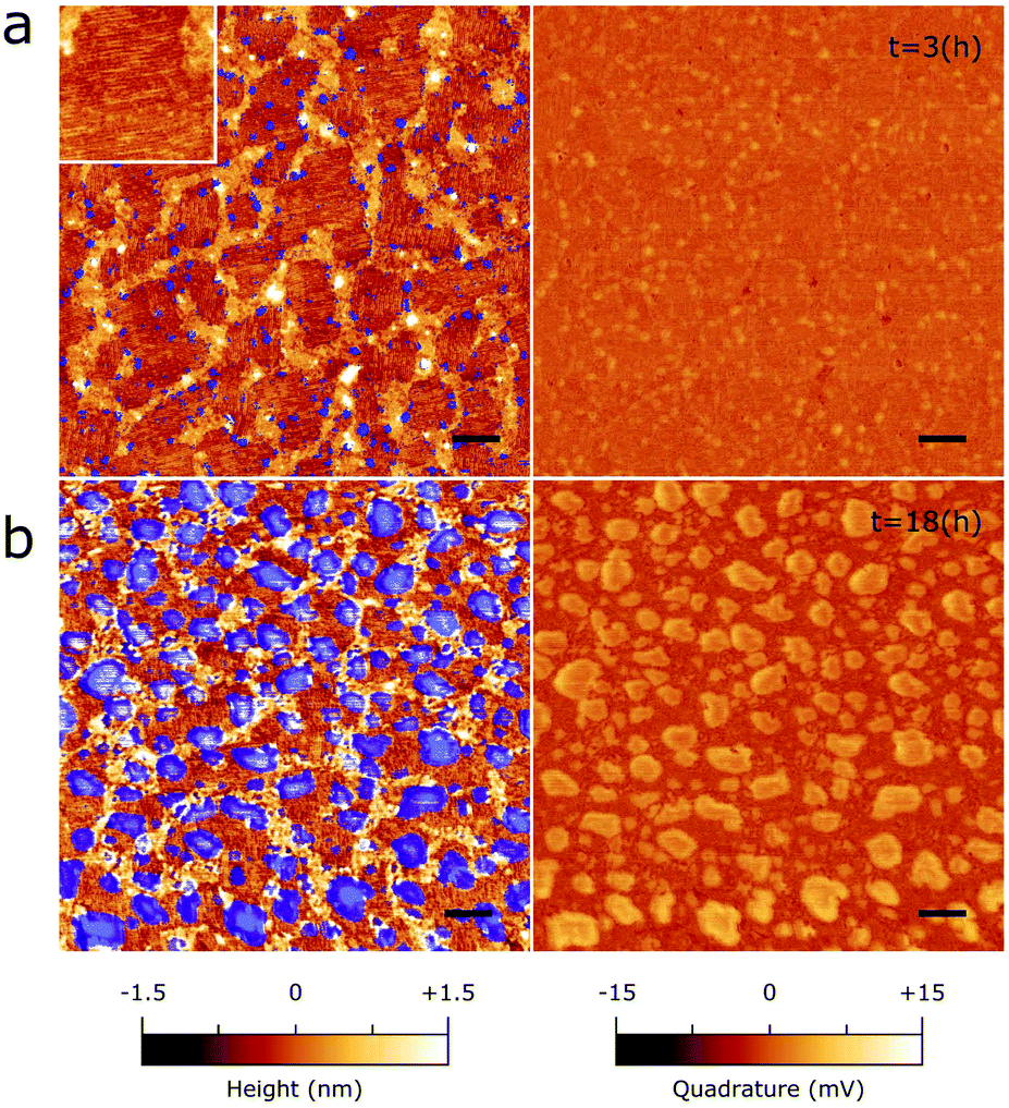 | ||
| Fig. 6 Inhibition of the 2D bP oxidation by epitaxial C24 multilayers. Topography (left) and peakforce quadrature signal (right) of a 1 μm2 area of a 2D bP flake functionalized with multilayered C24 exposed to humid air for 3 h (a) or 18 h (b). Scale bar is 100 nm. Inset of panel (a) is 150 × 150 nm. Areas highlighted in blue in the morphology micrographs correspond to the top 30% percentile of quadrature signal intensities, ascribable to the mechanically softer oxidized “bubble-like” zones (see Fig. 1 and 4). | ||
No apparent changes were detected during the first 3 hours of exposition. Fig. 6a shows a typical multilayered C24/2D bP flake after 3 hours of exposure to humid air. While the topographic AFM image does not seem to show any of the usual features associated with bP oxidation, small areas of an appreciable signal contrast start to emerge in the peakforce quadrature micrograph (Fig. 6a), signaling the first stages of the oxidation process. Marking the positions of the oxidized zones on the topography micrograph (blue markings in the left panel of Fig. 6) gives evidence that oxidation almost exclusively occurs at the boundaries between epitaxially ordered and disordered C24 domains, suggesting a depletion of C24 occurring in these zones, perhaps due to lateral rearrangement.
AFM was then recorded on the same sample and in the same area, after 18 hours of air exposure. Oxidation of bP was found to have progressed considerably. However, a significant fraction of the ordered domains remains unperturbed by oxidation, suggesting that C24 ordered multilayers are significantly more effective in inhibiting oxidation than C24 monolayers. With respect to bare bP, the pervasiveness of oxidation features is delayed by 18 hours (instead of 1 hour).
A likely interpretation is that epitaxial C24 molecules form a barrier between bP and the ambient environment, which does not allow the permeation of oxidizing gases like ambient O2 and H2O. This barrier is much more effective in epitaxial domains than in disordered ones (likely due to their more dense packing), which are in turn less prone to oxidation than interstitial areas between adjoining ordered and disordered zones. Therefore, the most important technical issue to ensure a good protection from oxidation is to minimize defects coverage at the boundaries between molecular domains with different ordering and orientations, which prevents a significant long-term stability (>24 h) of the C24 alkane/2D bP epitaxial system.
Electrical characterization of the tetracosane/2D bP heterostructure
We used electrostatic force microscopy (EFM) to investigate the electrical properties of pristine and alkane-coated 2D bP flakes of similar lateral and vertical dimensions immediately after preparation and after exposure to air on a conductive doped Si substrate (Fig. 7). For all samples, EFM maps were recorded at a constant height of 100 nm above the topography profile, thus preventing a direct contact between the tip and substrate, and keeping a +2 V bias between the tip and sample.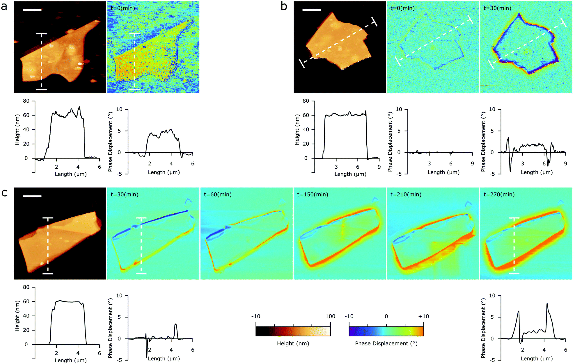 | ||
| Fig. 7 Influence of mono- or multi-layered C24 on the oxidation kinetics of 2D bP flakes as determined by electrostatic force microscopy. AFM and EFM micrographs and relative plots refer to (a) pristine 2D bP, (b) 2D bP coated with a C24 monolayer, and (c) 2D bP coated with a C24 multilayer. Within each panel, the row contains: a representative AFM topography micrograph of a 2D bP flake prior to exposure to humid air (leftmost image in black-brown-white false colour scale) and EFM scans of the same flake performed after specified oxidation times (successive images in blue-green-red scale). Scale bars are 2 μm. The Z scale of EFM scans represents the local phase displacement of the noncontact second pass scan with respect to the empty surface areas (average Z value of empty substrate = 0°). When a white dashed line is present in an image, a profile of the Z values measured along that line is presented below the image. | ||
The probe oscillated at the same resonant frequency as that used during the intermittent contact topographic scan while plotting oscillation phase displacements induced by local electrostatic forces. While a quantitative interpretation of the EFM maps is complicated due to the variability of several parameters (flake thickness, flake/substrate contact, C24 layer homogeneity and/or thickness, …), the presented data support the qualitative conclusion that: (i) alkane coating is able to significantly depress superficial bP polarization; (ii) the bP oxidation process impacts on its electrical properties; (iii) the multilayered C24 offers excellent protection against oxidation.
Fig. 7a shows how immediately after exfoliation pristine bP gives an appreciable change in the phase of oscillation (EFM contrast) with respect to the Si substrate. The EFM response of the substrate could be attributed to the nanometer thick layer of native SiOx on the Si surface. Conversely, even a C24 monolayer is sufficient to completely suppress the bP polarization (Fig. 7b, second panel and corresponding profile plot). This suggests that a single C24 monolayer responds to electrostatic stimuli as expected in the case of an electrical insulator. In principle, this may allow the implementation of C24 monolayer as a nano-insulator or even as a nanodielectric in 2D bP-based components and devices with a metal/insulator/semiconductor (MIS) structure.
Evolution of the EFM phase shift maps upon exposure of the 2D bP samples to air gives qualitative estimates of oxidation dynamics and the relative characteristics of inhibition of oxidation of C24 mono- and multilayers. After 30 minutes of exposition, 2D bP coated with a C24 monolayer already shows an appreciable average EFM phase shift with respect to the Si substrate (Fig. 7b, right EFM map), but multilayered C24/2D bP is still largely unperturbed (Fig. 7c, first EFM micrograph) and starts to show modulation of the collected signal after 150 min. Extended changes in the EFM signal of the flake surface are not appreciable before 270 minutes (see successive panels of Fig. 7c). Interestingly, most of the EFM signal change is localized at the sidewalls of bP flakes, which are most probably not protected by epitaxially ordered C24.
Conclusions
In conclusion, we studied the morphological and electrical characteristics and stability in air of a vdW epitaxial system based on 2D bP coated with tetracosane, a linear alkane with 24 carbon atoms. High resolution AFM of a model system composed of a monolayer of C24 on a bulk bP crystal revealed a high coverage of the bP surface with epitaxial domains of C24 over areas with lateral size greater than 1 μm2. The epitaxial domains are composed of C24 molecules ordered in a typical lamellar arrangement with periodicities that are in excellent agreement with single crystal XRD data of C24 and with alignment along the diagonal of the bP rectangular unit cell. Mechanically exfoliated 2D bP on silicon substrates were readily coated from solution with a monolayer and multilayers of C24. The ordering direction of the C24 molecules was the same as in the model system, and it extended from the interface along the multilayer thickness (2 nm). However, the dimensions of the epitaxial domains were smaller (lateral size around 100–200 nm).Our AFM studies have shown that the epitaxial C24 multilayers delay the oxidation of 2D bP in air by 18 hours, compared to 1 hour for bare 2D bP. The C24 epitaxial monolayers and disordered domains showed a much less efficient protection. MD simulations supported experimental data and confirmed that C24/bP interactions at the interface were dominated by van der Waals forces. Our simulations reveal two different global minima for the thermodynamic adsorption of the C24 chains on bP, with preferential orientations of the C24 molecules along the zig-zag and the diagonal directions of the bP rectangular unit cell. However, the difference between the two minima is comparable to the thermal energy and only one (the diagonal) preferential orientation was observed experimentally. Finally, EFM revealed that the C24 coating significantly depresses bP polarization and behaves as an electrical insulator as well as a protecting agent against oxidation. Further investigations using different processing techniques or other linear alkanes may lead to the minimization of defects on the 2D bP surface and on the coverage thus allowing a real long-term stability (greater than 24 h) of the alkane/2D bP epitaxial system. In addition, the implementation of functional groups on the linear alkane backbone would allow to tune its polarizability and obtain a high-performing nanodielectric layer. Overall, the presented work demonstrates a new example of a 2D van der Waals heterostructure corresponding to an insulator (alkane)-semiconductor (bP) stack, which has potential for integration within devices relevant to miro- and nanoelectronic, photonic and optoelectronic applications.
Conflicts of interest
There are no conflicts to declare.Acknowledgements
The European Research Council (ERC) and the National Research Council of Italy (CNR) are acknowledged for funding the work through the project PHOSFUN, an ERC Advanced Grant assigned to MP as PI (Grant Agreement No. 670173), an ERC Consolidator Grant assigned to EB as PI (Grant Agreement No. 307755).Notes and references
- V. Tran, R. Soklaski, Y. Liang and L. Yang, Phys. Rev. B: Condens. Matter Mater. Phys., 2014, 89, 235319 CrossRef; S. Fukuoka, T. Taen and T. Osada, J. Phys. Soc. Jpn., 2015, 84, 121004 CrossRef.
- Y. Takao and A. Morita, Physica B+C, 1981, 105, 93 CrossRef CAS; L. Liang, J. Wang, W. Lin, B. G. Sumpter, V. Meunier and M. Pan, Nano Lett., 2014, 14, 6400 CrossRef.
- Y. Maruyama, S. Suzuki, K. Kobayashi and S. Tanuma, Physica B+C, 1981, 105, 99 CrossRef CAS; D. Warschauer, J. Appl. Phys., 1963, 34, 1853 CrossRef; R. W. Keyes, Phys. Rev., 1953, 92, 580 CrossRef.
- J. Na, Y. T. Lee, J. A. Lim, D. K. Hwang, G.-T. Kim, W. K. Choi and Y.-W. Song, ACS Nano, 2014, 8, 11753 CrossRef CAS; H. Wang, X. Wang, F. Xia, L. Wang, H. Jiang, Q. Xia, M. L. Chin, M. Dubey and S.-J. Han, Nano Lett., 2014, 14, 6424 CrossRef; Y. Du, H. Liu, Y. Deng and P. D. Ye, ACS Nano, 2014, 8, 10035 CrossRef.
- S. Tran, J. Yang, N. Gillgren, T. Espiritu, Y. Shi, K. Watanabe, T. Taniguchi, S. Moon, H. Baek, D. Smirnov, M. Bockrath, R. Chen and C. N. Lau, Sci. Adv., 2017, 3, e1603179 CrossRef CAS; T. A. Ameen, H. Ilatikhameneh, G. Klimeck and R. Rahman, Sci. Rep., 2016, 6, 28515 CrossRef.
- H. Wang, X. Wang, F. Xia, L. Wang, H. Jiang, Q. Xia, M. L. Chin, M. Dubey and S.-J. Han, Nano Lett., 2014, 14, 6424 CrossRef CAS.
- J. Wu, G. K. W. Koon, D. Xiang, C. Han, C. T. Toh, E. S. Kulkarni, I. Verzhbitskiy, A. Carvalho, A. S. Rodin, S. P. Koenig, G. Eda, W. Chen, A. H. Castro Neto and B. Özyilmaz, ACS Nano, 2015, 9, 8070 CrossRef CAS.
- L. Li, Y. Yu, G. J. Ye, Q. Ge, X. Ou, H. Wu, D. Feng, X. H. Chen and Y. Zhang, Nat. Nanotechnol., 2014, 9, 372 CrossRef CAS.
- I. Kriegel, S. Toffanin and F. Scotognella, Appl. Opt., 2016, 55, 9288 CrossRef CAS; M. A. Huber, F. Mooshammer, M. Plankl, L. Viti, F. Sandner, L. Z. Kastner, T. Frank, J. Fabian, M. S. Vitiello, T. L. Cocker and R. Huber, Nat. Nanotechnol., 2016, 12, 207 CrossRef; J. Y. Lee, J.-H. Shin, G.-H. Lee and C.-H. Lee, Nanomaterials, 2016, 6, 193 CrossRef.
- W. Luo, D. Y. Zemlyanov, C. A. Milligan, Y. Du, L. Yang, Y. Wu and P. D. Ye, Nanotechnology, 2016, 27, 434002 CrossRef PubMed.
- J. D. Wood, S. A. Wells, D. Jariwala, K.-S. Chen, E. K. Cho, V. K. Sangwan, X. Liu, L. J. Lauhon, T. J. Marks and M. C. Hersam, Nano Lett., 2014, 14, 6964 CrossRef CAS.
- J. E. S. Fonsaca, S. H. Domingues, E. S. Orth and A. J. G. Zarbin, Sci. Rep., 2017, 7, 10165 CrossRef CAS; E. Passaglia, F. Cicogna, F. Costantino, S. Coiai, S. Legnaioli, G. Lorenzetti, S. Borsacchi, M. Geppi, F. Telesio, S. Heun, A. Ienco, M. Serrano-Ruiz and M. Peruzzini, Chem. Mater., 2018, 30, 2036 CrossRef; F. Telesio, E. Passaglia, F. Cicogna, F. Costantino, M. Serrano-Ruiz, M. Peruzzini and S. Heun, Nanotechnology, 2018, 29, 295601 CrossRef.
- S. Kuriakose, T. Ahmed, S. Balendhran, V. Bansal, S. Sriram, M. Bhaskaran and S. Walia, 2D Mater., 2018, 5, 032001 CrossRef; V. Artel, Q. Guo, H. Cohen, R. Gasper, A. Ramasubramaniam, F. Xia and D. Naveh, npj 2D Mater. Appl., 2017, 1, 6 CrossRef.
- X. Chen, Y. Wu, Z. Wu, Y. Han, S. Xu, L. Wang, W. Ye, T. Han, Y. He, Y. Cai and N. Wang, Nat. Commun., 2015, 6, 7315 CrossRef CAS; Y. Deng, Z. Luo, N. J. Conrad, H. Liu, Y. Gong, S. Najmaei, P. M. Ajayan, J. Lou, X. Xu and P. D. Ye, ACS Nano, 2014, 8, 8292 CrossRef; K. Tang, W. Qi, Y. Li and T. Wang, J. Phys. Chem. C, 2018, 122, 7027 CrossRef; K. Tang, W. Qi, Y. Li and T. Wang, Phys. Chem. Chem. Phys., 2018, 20, 29333 RSC; B. Liu, M. Long, M.-Q. Cai and J. Yang, Appl. Phys. Lett., 2018, 112, 043901 CrossRef; Y. Chen and S. Y. Quek, 2D Mater., 2018, 5, 045031 CrossRef; L. Huang and J. Li, Appl. Phys. Lett., 2016, 108, 083101 CrossRef.
- A. K. Geim and I. V. Grigorieva, Nature, 2013, 499, 419 CrossRef CAS PubMed; J. Yuan, S. Najmaei, Z. Zhang, J. Zhang, S. Lei, P. M. Ajayan, B. I. Yakobson and J. Lou, ACS Nano, 2015, 9, 555 CrossRef; A. Carvalho, M. Wang, X. Zhu, A. S. Rodin, H. Su and A. H. Castro Neto, Nat. Rev. Mater., 2016, 1, 16061 CrossRef.
- J. Sun, H.-W. Lee, M. Pasta, H. Yuan, G. Zheng, Y. Sun, Y. Li and Y. Cui, Nat. Nanotechnol., 2015, 10, 980 CrossRef CAS.
- M. Zhu, Z. Sun, M. Fujitsuka and T. Majima, Angew. Chem., Int. Ed., 2018, 57, 2160 CrossRef CAS PubMed.
- G. Abellán, V. Lloret, U. Mundloch, M. Marcia, C. Neiss, A. Görling, M. Varela, F. Hauke and A. Hirsch, Angew. Chem., Int. Ed., 2016, 55, 14557 CrossRef PubMed; Y. Zhao, Q. Zhou, Q. Li, X. Yao and J. Wang, Adv. Mater., 2017, 29, 1603990 CrossRef.
- C. R. Ryder, J. D. Wood, S. A. Wells, Y. Yang, D. Jariwala, T. J. Marks, G. C. Schatz and M. C. Hersam, Nat. Chem., 2016, 8, 597 CrossRef CAS PubMed.
- V. V. Korolkov, I. G. Timokhin, R. Haubrichs, E. F. Smith, L. Yang, S. Yang, N. R. Champness, M. Schröder and P. H. Beton, Nat. Commun., 2017, 8, 1385 CrossRef CAS; P. Vishnoi, S. Rajesh, S. Manjunatha, A. Bandyopadhyay, M. Barua, S. K. Pati and C. N. R. Rao, ChemPhysChem, 2017, 18, 2985 CrossRef PubMed; C. Wang, D. Niu, B. Liu, S. Wang, X. Wei, Y. Liu, H. Xie and Y. Gao, J. Phys. Chem. C, 2017, 121, 18084 CrossRef.
- A. Facchetti and T. J. Marks, Mater. Lett., 2009, 4, 64 Search PubMed; W. W. A. Koopman, S. Toffanin, M. Natali, S. Troisi, R. Capelli, V. Biondo, A. Stefani and M. Muccini, Nano Lett., 2014, 14, 1695 CrossRef CAS.
- M. Durso, C. Bettini, A. Zanelli, M. Gazzano, M. G. Lobello, F. De Angelis, V. Biondo, D. Gentili, R. Capelli, M. Cavallini, S. Toffanin, M. Muccini and M. Melucci, Org. Electron., 2013, 14, 3089 CrossRef CAS; T. Benincori, V. Bonometti, F. De Angelis, L. Falciola, M. Muccini, P. R. Mussini, T. Pilati, G. Rampinini, S. Rizzo, S. Toffanin and F. Sannicolò, Chem. – Eur. J., 2010, 16, 9086 CrossRef PubMed; M. Bolognesi, M. Prosa, M. Tessarolo, G. Donati, S. Toffanin, M. Muccini and M. Seri, Sol. Energy Mater. Sol. Cells, 2016, 155, 436 CrossRef.
- T. Zhang, Z. Cheng, Y. Wang, Z. Li, C. Wang, Y. Li and Y. Fang, Nano Lett., 2010, 10, 4738 CrossRef CAS; S. A. Svatek, O. R. Scott, J. P. H. Rivett, K. Wright, M. Baldoni, E. Bichoutskaia, T. Taniguchi, K. Watanabe, A. J. Marsden, N. R. Wilson and P. H. Beton, Nano Lett., 2015, 15, 159 CrossRef.
- H.-M. Zhang, Z.-X. Xie, B.-W. Mao and X. Xu, Chem. – Eur. J., 2004, 10, 1415 CrossRef CAS.
- H. Schollmeyer, B. Struth and H. Riegler, Langmuir, 2003, 19, 5042 CrossRef CAS.
- A. Ciesielski, S. Haar, M. El Gemayel, H. Yang, J. Clough, G. Melinte, M. Gobbi, E. Orgiu, M. V. Nardi, G. Ligorio, V. Palermo, N. Koch, O. Ersen, C. Casiraghi and P. Samorì, Angew. Chem., Int. Ed., 2014, 53, 10355 CrossRef CAS; F. Thibaudau, G. Watel and J. Cousty, Surf. Sci. Lett., 1993, 281, L303 CrossRef; G. C. McGonigal, R. H. Bernhardt and D. J. Thomson, Appl. Phys. Lett., 1990, 57, 28 CrossRef; A. Wawkuschewski, H.-J. Cantow and S. N. Magonov, Langmuir, 1993, 9, 2778 CrossRef; B. Michel, G. Travaglini, H. Rohrer, C. Joachim and M. Amrein, Z. Phys. B Condens. Matter, 1989, 76, 99 CrossRef; R. Yamada and K. Uosaki, J. Phys. Chem. B, 2000, 104(25), 6021 CrossRef; S. Haar, M. Bruna, J. X. Lian, F. Tomarchio, Y. Olivier, R. Mazzaro, V. Morandi, J. Moran, A. C. Ferrari, D. Beljonne, A. Ciesielski and P. Samorì, J. Phys. Chem. Lett., 2016, 7, 2714 CrossRef.
- PubChem, Open Chemistry Database, Compound Summary for CID 12592 Tetracosane, https://pubchem.ncbi.nlm.nih.gov/compound/tetracosane, accessed: 11, 2018.
- S. Lange, P. Schmidt and T. Nilges, Inorg. Chem., 2007, 46, 4028 CrossRef CAS.
- D. Nečas and P. Klapetek, Cent. Eur. J. Phys., 2012, 10, 181 Search PubMed.
- V. Sresht, A. A. H. Pádua and D. Blankschtein, ACS Nano, 2015, 9, 8255 CrossRef CAS.
- S. W. I. Siu, K. Pluhackova and R. A. Böckmann, J. Chem. Theory Comput., 2012, 8, 1459 CrossRef CAS.
- S. Plimpton, J. Comput. Phys., 1995, 117, 1 CrossRef CAS.
- A. Lorenzoni, A. Mosca Conte, A. Pecchia and F. Mercuri, Nanoscale, 2018, 10, 9376 RSC.
- J. O. Island, G. A. Steele, H. S. J. van der Zant and A. Castellanos-Gomez, 2D Mater., 2015, 2, 011002 CrossRef.
- J.-S. Kim, Y. Liu, W. Zhu, S. Kim, D. Wu, L. Tao, A. Dodabalapur, K. Lai and D. Akinwande, Sci. Rep., 2015, 5, 8989 CrossRef CAS PubMed.
- A. R. Gerson and S. C. Nyburg, Acta Crystallogr., Sect. B: Struct. Sci., 1992, 48, 737 CrossRef (single crystal, Deposition Number CCDC 1319744†).
- C. D. Zhang, J. C. Lian, W. Yi, Y. H. Jiang, L. W. Liu, H. Hu, W. D. Xiao, S. X. Du, L. L. Sun and H. J. Gao, J. Phys. Chem. C, 2009, 113, 18823 CrossRef CAS.
- A. Favron, E. Gaufrès, F. Fossard, A.-L. Phaneuf-L'Heureux, N. Y.-W. Tang, P. L. Lévesque, A. Loiseau, R. Leonelli, S. Francoeur and R. Martel, Nat. Mater., 2015, 14, 826 CrossRef CAS.
- J. D. Albar, V. V. Korolkov, M. Baldoni, K. Watanabe, T. Taniguchi, E. Besley and P. H. Beton, J. Phys Chem. C, 2018, 122, 27575 CrossRef CAS.
Footnote |
| † Electronic supplementary information (ESI) available. See DOI: 10.1039/c9nr01155b |
| This journal is © The Royal Society of Chemistry 2019 |