 Open Access Article
 This Open Access Article is licensed under a
 Creative Commons Attribution 3.0 Unported Licence
Interactions of Pb and Te atoms with graphene
Chuncheng
Gong
,
Alex W.
Robertson
,
Kuang
He
,
Camden
Ford
,
Andrew A. R.
Watt
and
Jamie H.
Warner
*
Department of Materials, University of Oxford, Parks Road, Oxford, OX1 3PH, UK. E-mail: Jamie.warner@materials.ox.ac.uk
First published on 20th February 2014
Abstract
PbTe nanocrystals were deposited onto the surface of graphene and used as a reservoir of Pb and Te atoms. Electron beam irradiation at 80 kV caused Pb and Te atoms to mobilize and disperse across the surface of graphene. We studied the dynamics of these atoms in real time using aberration-corrected transmission electron microscopy. The Pb and Te atoms were found to attach to the surface layer of amorphous carbon that resides upon the graphene, as well as its edge. Pb and Te atoms were not found residing on pristine graphene, but were found to bond to the free edge states along graphene hole edges. Small PbTe nanoclusters tended to only form on the surface of the amorphous carbon regions and not on pristine graphene.
Graphene is a two-dimensional crystal and is essentially a surface with no volume.1 This inherent property of 2D materials makes them highly sensitive to attachment of atomic surface species. Surface atoms attached to graphene can modify its electronic properties by doping, causing shifts in the Dirac point,2 and possibly inducing magnetism if the surface atoms form magnetic species.3,4 However, doping does have a positive role in reducing the sheet resistance of monolayer graphene, which is important for its implementation as a transparent conducting electrode in solar cells, LEDs and touch-screens.5–7 Understanding the atomic configuration of surface adatoms on graphene may help develop graphene with further reductions in its sheet resistance and consequently better performance in devices. Metal atoms are often found on the surface of graphene grown by chemical vapour deposition on a metal catalyst and also dope graphene. The fundamental interactions between metal atoms and graphene is also of importance to catalytic reactions, where the metal nanoparticles or clusters reside on a graphitic support.8
The atomic structure of graphene can be imaged non-destructively using aberration-corrected transmission electron microscopy (AC-TEM) at low accelerating voltages of ≤80 kV.9,10 Apart from observing the standard pristine hexagonal atomic structure of sp2 graphene lattice, it is also possible to image vacancies and defects in graphene by AC-TEM. Surface adatoms may also be observed on graphene when imaging by AC-TEM, which in the majority of cases are carbon, nitrogen and oxygen, the main residues from the polymer used in the chemical vapour deposition (CVD) transfer process or any remaining solvent left over from chemical exfoliation.11,12 Some heavier surface adatoms are also found on graphene, such as Si, Na or Fe.13–16 TEM studies have been previously performed on the migratory behaviour of heavy metal atoms, including tungsten, gold and platinum, on the graphene surface.17,18 These looked at the effect of the sample temperature and the strain of the graphene substrate on the metal adatom movement. This has been further extended into imaging dopants that are within the graphene lattice and bonded to carbon atoms, such as Si or Fe.19–22 Such covalently bonded defects have a significantly lower diffusion rate, and were found to be relatively stable in comparison to the weakly interacting surface adatoms.19,23,24 The increased stability conferred by in-plane covalent bonding suggests that any mobile surface adatom species will tend to diffuse and localise around any exposed under-coordinated elements, such as graphene edges.
In this report, we examine heavy atoms, Pb and Te, on the surface of graphene using AC-TEM. We use PbTe nanocrystals as the source of the Pb and Te atoms and upon electron beam exposure, Pb and Te atoms are released onto the graphene surface. We study the positions where the atoms remain stable, and the pathways for movement along the surface.
Graphene was grown by CVD using a liquid Cu catalyst, as previously reported.25 It was then transferred to silicon nitride TEM grids with 2 micron diameter holes by a polymer supporting scaffold layer.26,27 PbTe nanocrystals were synthesized using solution phase methods, as previously reported. The PbTe nanocrystals were drop-cast onto the graphene surface and upon drying self-assembled into small closed-packed regions, as shown in Fig. 1a. Fig. 1b shows a higher magnification AC-TEM image of the PbTe nanocrystals and their lattice planes easily resolved. The oleic acid and TOP surface passivating ligands result in the uniform separation between the nanocrystals.
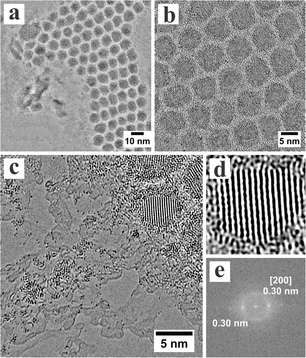 | ||
| Fig. 1 (a) TEM image of PbTe quantum dots on graphene sheets; (b) higher magnification of PbTe nanocrystals with the diameters of about 5 nm; (c) TEM image of disordered Pb and Te atoms driven by electron beam irradiation from several PbTe nanocrystals near the edge of a graphene sheet; (d) AC-TEM image of one single PbTe nanocrystal; (e) Fast Fourier transform (FFT) of image (d) showing lattice spots correspond to [200] plane of rock salt PbTe structure. | ||
We found that irradiation of the edge regions of the closed-packed arrays of nanocrystals resulted in the release of substantial Pb and Te atoms from the nanocrystals. In Fig. 1c, the strong dark contrast spots correspond to Pb and Te atoms. It is difficult to differentiate between Pb and Te atoms based purely on contrast intensity in AC-TEM. The heavy atoms are found as isolated single atoms, but also as small clusters in Fig. 1c. Fig. 1d shows an AC-TEM image of a single PbTe nanocrystals with lattice spacing of 0.3 nm, Fig. 1e, corresponding to the [200] PbTe rock-salt lattice plane at 0.32 nm.28
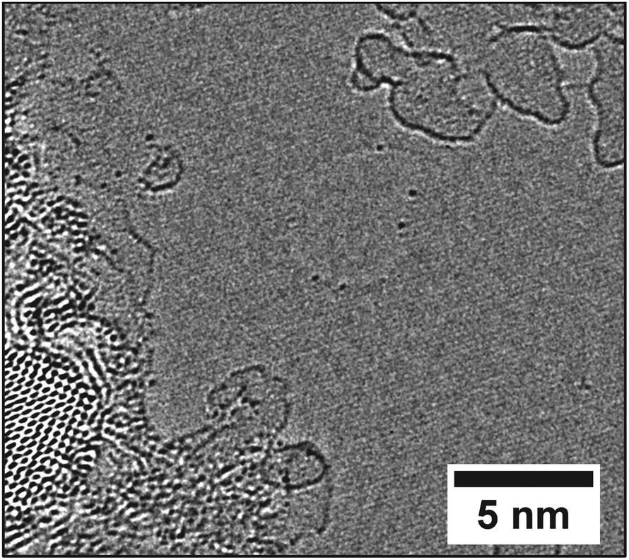
The electron-beam induced release of atoms come from the edges of the nanocrystals and also the surrounding surface capping ligands, which are likely to also contain some metal–ligand complexes. We found that the heavy atoms were only stable in fixed positions around and on top of the amorphous carbon residue that sits on graphene. This is shown more clearly in Fig. 2a, where defocus has increased the contrast of the edges of the surface amorphous carbon, as indicated by the black arrow. A hole within the graphene sheet is also visible in Fig. 2a (white arrow) and heavy Pb or Te atoms are attached to the edges of the graphene hole. We found no evidence that Pb or Te atoms could remain fixed in a stable location on the pristine lattice of graphene. We did find Pb and Te atoms on islands of amorphous carbon that were isolated from the main nanocrystals area, indicating that Pb or Te atoms were highly mobile across the pristine graphene and could travel from island to island of amorphous carbon.
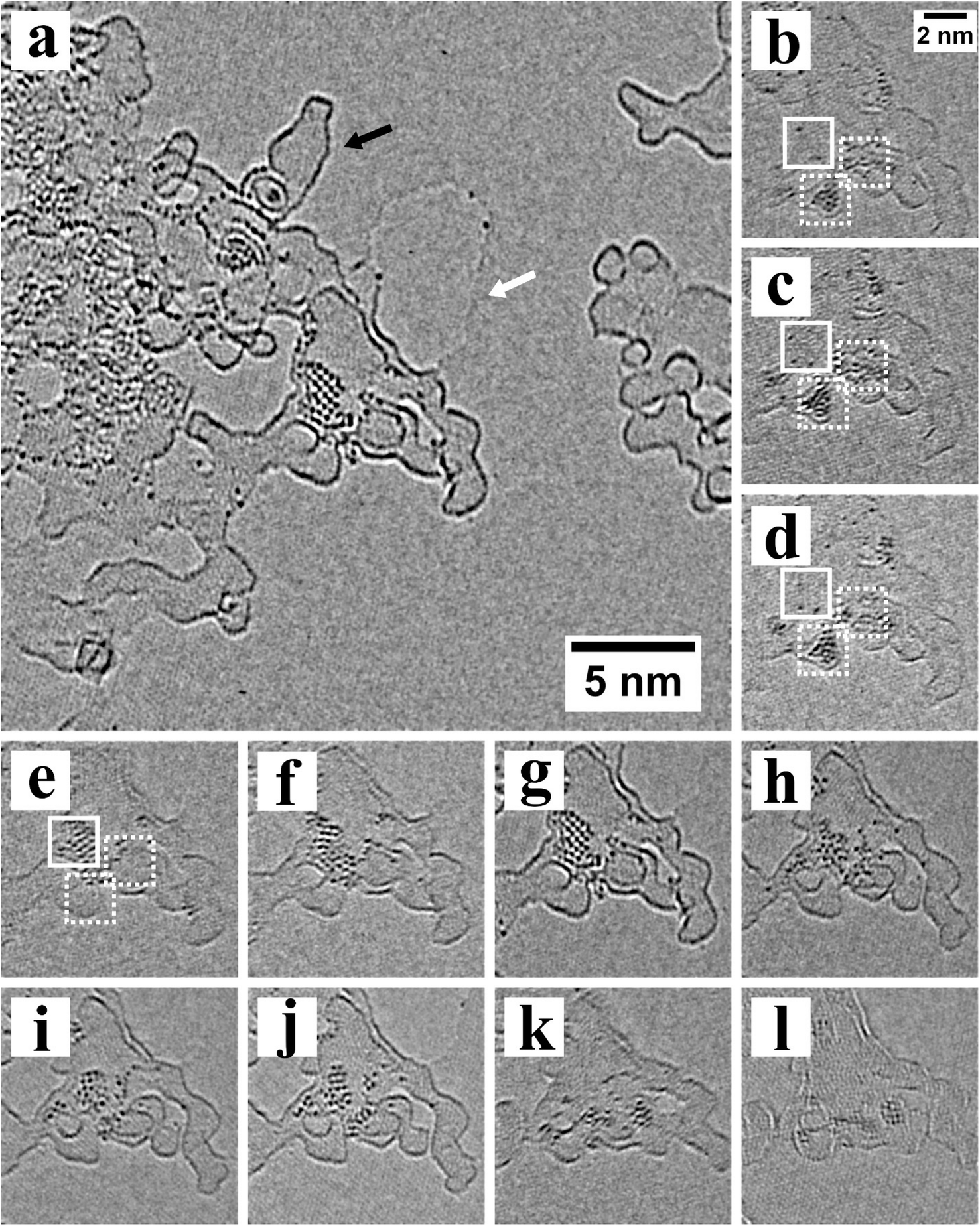 | ||
| Fig. 2 (a) AC-TEM image of the graphene with heavy atoms on amorphous carbon and edges; (b–l) time sequence of the motion and structure of Pb and Te atoms on amorphous carbon. Time between frames is 10 s. | ||
Electron beam irradiation provides the energy for movement of Pb and Te atoms on amorphous carbon and in some cases we observed the recrystallization of the Pb and Te atoms into small nanocrystals, as observed in Fig. 2a. Fig. 2b–l show the time-series of images that reveal the crystal formation. Dozens of those heavy atoms agglomerate on amorphous carbon to form nanocrystals, whose crystal orientation varies as a function of time according to the time sequence images. Pb and Te atoms first form two nanoclusters marked by the dotted white square in Fig. 2b, and then continue to grow and connected together in Fig. 2d. Afterwards, the nanocrystals keeps growing and the atoms in the dotted square begin to migrate to the full square in Fig. 2e. In Fig. 2d–j, the degree of order and orientation keeps changing, indicating that the nanocrystals is highly unstable. In Fig. 2g a highly ordered nanocrystal is formed with 2 slightly different crystal orientation, which is likely affected by the edge of amorphous carbon where heavy atoms first aggregate and nucleate. In Fig. 2h–l, the number of atoms on amorphous carbon continue to decrease. The whole process from Fig. 2b–k takes less than 100 seconds.
The formation of small nanoclusters and nanocrystals of Pb and Te atoms only occurred on the surface of the amorphous carbon, and neither on the amorphous carbon edges or the surface of pristine graphene. We did not find more than one or two Pb or Te atoms attached to the edges of the amorphous carbon. The Pb and Te atoms on the surface of the amorphous carbon islands are likely to be more tightly bound than those attached to the edge and this could allow the build-up of atoms to form the necessary concentration to form a nanocluster. Pb or Te atoms attached to the edges of the amorphous carbon islands are able to be released by electron beam irradiation and migrate to the next island. This indicates that an amorphous carbon surface is better than pristine graphene lattice for the formation of small metastable nanoclusters and nanocrystals. This may have important ramifications in the formation of optimized metal catalysts on carbon supports for fuel cells.29
In order to identify the crystal structure on the amorphous carbon, Fig. 3a is extracted from Fig. 2g, the image of the nanocrystals and shows the separation between atomic columns for the horizontal directions. In Fig. 3b, the image has been rotated by 90 degrees clockwise, with the vertical separation between atomic columns reported. The average distance between atomic columns is 328 pm in Fig. 3a and 336 pm in Fig. 3b, which corresponded to the [200] plane of rock-salt PbTe crystal (323 pm).
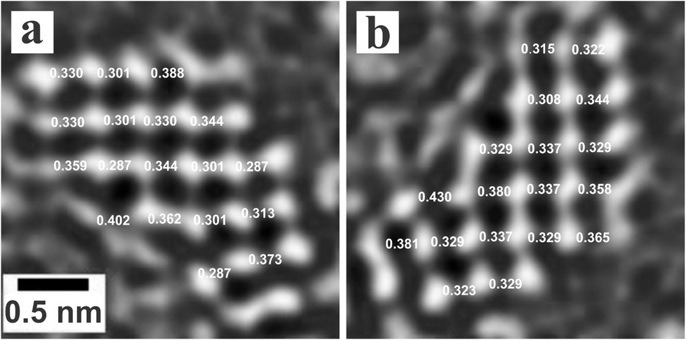 | ||
| Fig. 3 (a) Measurement of the distance between atomic columns for the nanocrystals observed in Fig. 2g. (b) The image in (a) has been rotated by 90 degrees clockwise. | ||
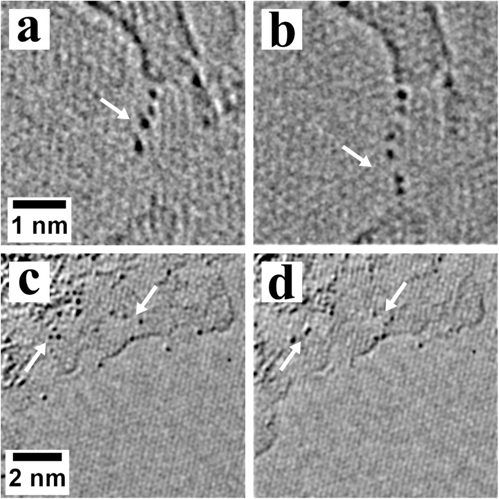
The edges of graphene, available due to the presence of a hole, provide in-plane covalent attachment sites for the Pb and Te atoms with some stability. Electron beam irradiation provides energy for the Pb and Te atoms to migrate around the edge of graphene. Fig. 4 shows the number and positions of heavy atoms on the edge of graphene changes as a function of time. Atom 1, 2 indicated by the white numbers in Fig. 4 remain motionless during the whole time, which act as references in these images. Atom 3 also exists through the whole period, while its position changes slightly. Other atoms indicated by a black number are only spotted in a few images.
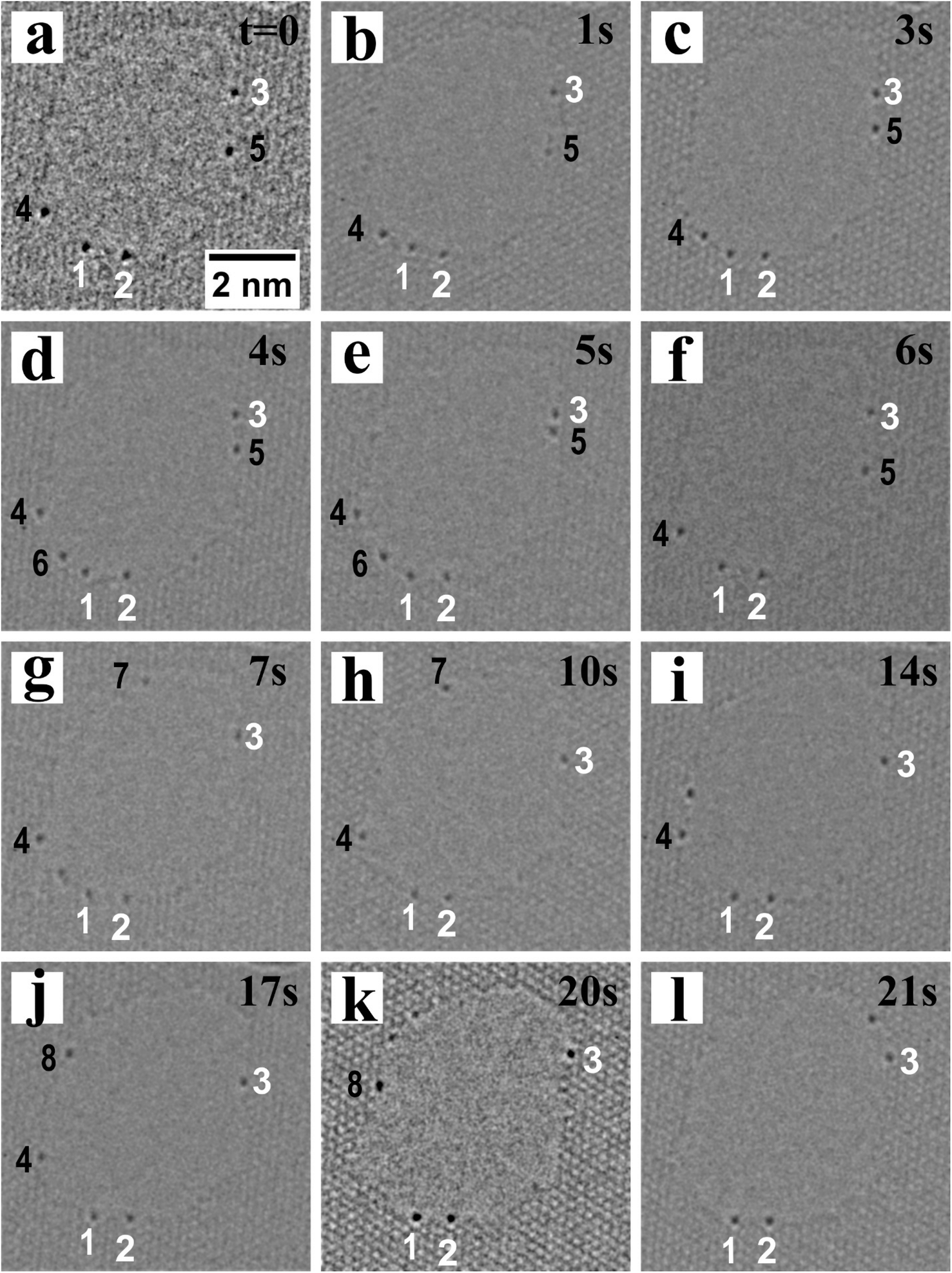 | ||
| Fig. 4 Time series of Pb or Te adatoms on the edge of graphene: atom marked by white numbers exist during the whole period; atoms marked by black numbers do not make the whole time. | ||
Fig. 5 shows the location of the hole in graphene with Pb and Te atoms, imaged in Fig. 4. The hole is about 5 nm from the nanocrystals, but separated by pristine graphene. The hole was created by electron beam irradiation and therefore the Pb and Te atoms attached to the hole must have originated from the nanocrystals region on the left. The lack of any heavy metal atoms isolated on the graphene sheet confirms that the Pb and Te atoms are highly mobile on the surface of graphene and are only stabilized to a fixed position at the edges of graphene or on the amorphous carbon residues. If these metal atoms were less mobile on the graphene surface we would expect to capture at least some metal atoms residing on the sheet during the course of the image exposure, however they remain concentrated at edge sites; either of the monolayer graphene or the mono- to few-layer amorphous carbon regions.
 | ||
| Fig. 5 AC-TEM image of a hole in graphene with Pb and Te atoms attached to the edge. | ||
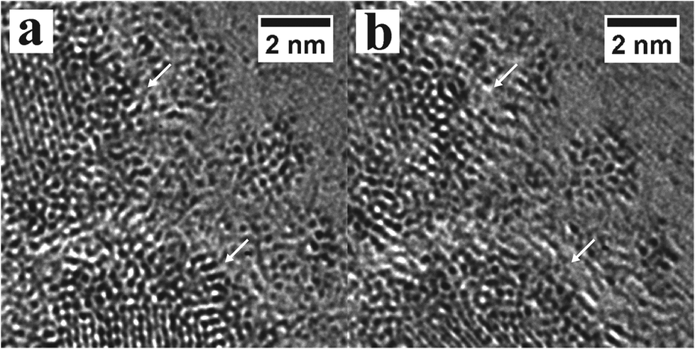
We now explore in more detail this propensity for the heavy atoms to also localize along the amorphous carbon edges, and to a lesser degree on the amorphous surface. Fig. 6 shows that the Pb and Te atoms attached to both the edge and top surface of the amorphous carbon islands also move under the electron beam. In Fig. 6a and b, heavy atoms are seen moving along the edge of the amorphous carbon. Pairs of atoms seem to have formed in Fig. 6b. Fig. 6c and 6d show Pb or Te atoms moving on the top surface of the amorphous carbon.
 | ||
| Fig. 6 Movement of Pb or Te atoms attached to amorphous carbon on graphene, indicated by white arrows (time between a and b, c and d is 10 s): (a, b) atoms move along the edge of amorphous carbon; (c, d) atoms move across the surface of amorphous carbon residing on graphene. | ||
The electron beam also induces movement of the atoms at the edge of the PbTe nanocrystals. Fig. 7 shows two AC-TEM images with 10 seconds separation in time, where regions of dark contrast associated with the Pb and Te atoms change, indicated by arrows. The electron beam can decompose the surface capping ligands and aid in release the Pb and Te atoms onto the surface of the graphene. Small clusters seem to form next to the PbTe nanocrystals.
 | ||
| Fig. 7 Movement of heavy atoms around the edges of the PbTe nanocrystals under electron beam irradiation at time (a) 0 seconds and (b) after 10 seconds. | ||
In summary, we have shown that Pb and Te atoms are highly mobile on pristine graphene surfaces and do not remain in fixed positions for any appreciable time. The Pb and Te atoms do remain fixed at the edges of graphene and also on the edges and top surface of amorphous carbon. The Pb and Te atoms are still mobile when attached to amorphous carbon and graphene edges, and simply rapidly migrate between locations of fixed stability. The ability to trap several Pb and Te atoms on the surface of the amorphous carbon resulted in electron beam induced coalescence and the formation of nanoclusters and occasionally PbTe nanocrystals. These results indicate that it will be challenging to form PbTe nanocrystals that are in direct contact with graphene, since the tendency is to stick to the top of the amorphous carbon residue. This provides important insights into the future development of graphene-inorganic composites for energy applications.
Methods
Graphene synthesis and transfer
Graphene monolayers were prepared by atmospheric pressure chemical vapour deposition (CVD). We used a molten copper sheet (Alfa Aesar, Puratonic 99.999% pure, 0.1 mm thick) of ∼1 cm2 for the catalyst, which was placed on a cm2 piece of molybdenum (Alfa Aesar, 99.95% pure, 0.1 mm thick) to act as a stable wetting layer. This was placed into the CVD furnace, and was pumped to vacuum then backfilled with Ar gas. 100 s.c.c.m. H2/Ar (20% H2 in Ar) and 200 s.c.c.m. 100% Ar was flowed. Once the furnace hot-zone temperature reached 1090 °C the sample was moved from the room-temperature region into the center and annealed for 30 min. The CH4 flow (1% CH4 in Ar) was switched on at 10 s.c.c.m, and the H2/Ar flow reduced from 100 to 80 s.c.c.m and the 100% Ar flow maintained at 200 s.c.c.m after the anneal. This growth phase was executed for 90 min to obtain a continuous film. When completed the CH4 flow was disabled and the sample immediately removed from the furnace hot zone for rapid cooling in the H2 and Ar atmosphere. This graphene/Cu/Mo stack had a PMMA scaffold (8 wt% in anisole, 495k molecular weight) spin-cast on to the graphene side of the sample at 4700 rpm for 60 s, and then cured at 180 °C for 90 s. The supporting Mo and Cu were etched by floating the sample on an FeCl3 + HCl solution for several days, until just a transparent PMMA/graphene film remained on the surface. The remaining polymer/graphene film was cleaned by transferring and floating onto fresh DI water several times. Following this the sample was transferred to a 30% HCl solution for 5 min and then rinsed again in DI water for 30 min. Finally the sample was transferred to a holey silicon nitride TEM grid (Agar Scientific Y5385). Once left to dry for about an hour, the sample was baked on a hotplate at 150 °C for 15 min to remove water and improve sample adhesion. The sample was then heated for 10 h in air at 300 °C in a tube furnace and then 10 h at 180 °C under a vacuum of 10−5 mbar to remove unwanted residue and PMMA from the graphene.PbTe nanocrystal synthesis and deposition
PbTe nanocrystals were synthesized following a previously reported method.30 The precursors used were PbO, 99.999%; trioctylphosphine (TOP), technical grade 90%; oleic acid, technical grade, 90%; Te shot, 1–2 mm, 99.99%; diphenyl ether, 99%. A precursor solution of 1 M Te–TOP was prepared by heating the Te and TOP to 100 °C and stirring overnight in a N2 atmosphere. Initially, a Pb–oleate solution was created by heating 3 mmol of PbO with 6 mL oleic acid and 14 mL of diphenyl ether. This was heated to 100 °C under vacuum, using a Schlenk line, for 1 h. The solution was then heated to 200 °C under nitrogen and 3 mL of Te–TOP precursor was injected. The system was quenched in ice after 10 s to stop the reaction. The nanocrystal solution was purified by first mixing in a 1![[thin space (1/6-em)]](https://www.rsc.org/images/entities/char_2009.gif) :1 ratio with hexane and then combined in a 3:1 ratio with ethanol. This solution was centrifuged at 6000 rpm for 10 min, with the supernatant solution being discarded and the nanocrystals re-dissolved in hexane. This process was then repeated once, but the nanocrystals were then re-dissolved in toluene at 30 mg mL−1 to use for spin coating. PbTe nanocrystals were deposited by drop casting onto clean graphene membranes transferred onto SiN TEM grids. Once the solvent had evaporated (∼1–2 min) hexane was applied by drop casting to remove unwanted excess reactants.
:1 ratio with hexane and then combined in a 3:1 ratio with ethanol. This solution was centrifuged at 6000 rpm for 10 min, with the supernatant solution being discarded and the nanocrystals re-dissolved in hexane. This process was then repeated once, but the nanocrystals were then re-dissolved in toluene at 30 mg mL−1 to use for spin coating. PbTe nanocrystals were deposited by drop casting onto clean graphene membranes transferred onto SiN TEM grids. Once the solvent had evaporated (∼1–2 min) hexane was applied by drop casting to remove unwanted excess reactants.
Electron microscopy
The Oxford-JEOL JEM-2200MCO FEGTEM with CEOS hexapole aberration correctors, at an accelerating voltage of 80 kV, was used for electron beam irradiation and imaging.Acknowledgements
J.H.W. thanks the support from the Royal Society and Balliol College, Oxford. C.G. is funded by the University of Oxford Clarendon Fund Scholarship. Financial support for A.W.R. was from EPSRC (Platform Grants EP/F048009/1 and EP/K032518/1) is gratefully acknowledged.References
- A. K. Geim and K. S. Novoselov, The Rise of Graphene, Nat. Mater., 2007, 6, 183–191 CrossRef CAS PubMed.
- M. Ishigami, J. H. Chen, W. G. Cullen, M. S. Fuhrer and E. D. Williams, Atomic Structure of Graphene on SiO2, Nano Lett., 2007, 7, 1643–1648 CrossRef CAS PubMed.
- O. Yazyev, Magnetism in Disordered Graphene and Irradiated Graphite, Phys. Rev. Lett., 2008, 101, 037203 CrossRef.
- A. V. Krasheninnikov, P. O. Lehtinen, A. S. Foster, P. Pyykkö and R. M. Nieminen, Embedding Transition-Metal Atoms in Graphene: Structure, Bonding, and Magnetism, Phys. Rev. Lett., 2009, 102, 126807 CrossRef CAS.
- A. H. Castro Neto, N. M. R. Peres, K. S. Novoselov and A. K. Geim, The Electronic Properties of Graphene, Rev. Mod. Phys., 2009, 81, 109–162 CrossRef CAS.
- S. Bae, H. Kim, Y. Lee, X. Xu, J.-S. Park, Y. Zheng, J. Balakrishnan, T. Lei, H. R. Kim and Y. Il Song, et al., Roll-to-Roll Production of 30-Inch Graphene Films for Transparent Electrodes, Nat. Nanotechnol., 2010, 5, 574–578 CrossRef CAS PubMed.
- X. Wang, L. Zhi and K. Müllen, Transparent, Conductive Graphene Electrodes for Dye-Sensitized Solar Cells, Nano Lett., 2008, 8, 323–327 CrossRef CAS PubMed.
- R. Zan, U. Bangert, Q. Ramasse and K. S. Novoselov, Metal - Graphene Interaction Studied via Atomic Resolution Scanning, Nano Lett., 2011, 1087–1092 CrossRef CAS PubMed.
- J. C. Meyer, C. Kisielowski, R. Erni, M. D. Rossell, M. F. Crommie and A. Zettl, Direct Imaging of Lattice Atoms and Topological Defects in Graphene Membranes, Nano Lett., 2008, 8, 3582–3586 CrossRef CAS PubMed.
- J. H. Warner, E. R. Margine, M. Mukai, A. W. Robertson, F. Giustino and A. I. Kirkland, Dislocation-Driven Deformations in Graphene, Science, 2012, 337, 209–212 CrossRef CAS PubMed.
- H. J. Park, J. Meyer, S. Roth and V. Skákalová, Growth and Properties of Few-Layer Graphene Prepared by Chemical Vapor Deposition, Carbon, 2010, 48, 1088–1094 CrossRef CAS PubMed.
- A. Pirkle, J. Chan, A. Venugopal, D. Hinojos, C. W. Magnuson, S. McDonnell, L. Colombo, E. M. Vogel, R. S. Ruoff and R. M. Wallace, The Effect of Chemical Residues on the Physical and Electrical Properties of Chemical Vapor Deposited Graphene Transferred to SiO2, Appl. Phys. Lett., 2011, 99, 122108 CrossRef PubMed.
- Y. Lee, S. Bae, H. Jang, S. Jang, S.-E. Zhu, S. H. Sim, Y. Il Song, B. H. Hong and J.-H. Ahn, Wafer-Scale Synthesis and Transfer of Graphene Films, Nano Lett., 2010, 10, 490–493 CrossRef CAS PubMed.
- Y.-J. Yu, Y. Zhao, S. Ryu, L. E. Brus, K. S. Kim and P. Kim, Tuning the Graphene Work Function by Electric Field Effect, Nano Lett., 2009, 9, 3430–3434 CrossRef CAS PubMed.
- M. F. Chisholm, G. Duscher and W. Windl, Oxidation Resistance of Reactive Atoms in Graphene, Nano Lett., 2012, 12, 4651–4655 CrossRef CAS PubMed.
- Q. M. Ramasse, R. Zan, U. Bangert, D. W. Boukhvalov, Y. Son and K. S. Novoselov, Direct Experimental Evidence of Metal-Mediated Etching of Suspended Graphene, ACS Nano, 2012, 6, 4063–4071 CrossRef CAS PubMed.
- Y. Gan, L. Sun and F. Banhart, One- and Two-Dimensional Diffusion of Metal Atoms in Graphene, Small, 2008, 4, 587–591 CrossRef CAS PubMed.
- O. Cretu, A. V. Krasheninnikov, J. A. Rodríguez-Manzo, L. Sun, R. M. Nieminen and F. Banhart, Migration and Localization of Metal Atoms on Strained Graphene, Phys. Rev. Lett., 2010, 105, 196102 CrossRef.
- W. Zhou, M. D. Kapetanakis, M. P. Prange, S. T. Pantelides, S. J. Pennycook and J.-C. Idrobo, Direct Determination of the Chemical Bonding of Individual Impurities in Graphene, Phys. Rev. Lett., 2012, 109, 206803 CrossRef.
- Q. Ramasse and C. Seabourne, Probing the Bonding and Electronic Structure of Single Atom Dopants in Graphene with Electron Energy Loss Spectroscopy, Nano Lett., 2012, 13, 4989–4995 CrossRef PubMed.
- U. Bangert, W. Pierce, D. M. Kepaptsoglou, Q. Ramasse, R. Zan, M. H. Gass, J. A. Van den Berg, C. B. Boothroyd, J. Amani and H. Hofsäss, Ion Implantation of Graphene-Toward IC Compatible Technologies, Nano Lett., 2013, 13, 4902–4907 CrossRef CAS PubMed.
- A. W. Robertson, B. Montanari, K. He, J. Kim, C. S. Allen, Y. A. Wu, J. Olivier, J. Neethling, N. Harrison and A. I. Kirkland, et al., Dynamics of Single Fe Atoms in Graphene Vacancies, Nano Lett., 2013, 13, 1468–1475 CAS.
- H. Wang, Q. Wang, Y. Cheng, K. Li, Y. Yao, Q. Zhang, C. Dong, P. Wang, U. Schwingenschlögl and W. Yang, et al., Doping Monolayer Graphene with Single Atom Substitutions, Nano Lett., 2012, 12, 141–144 CrossRef CAS PubMed.
- H. Wang, K. Li, Y. Cheng, Q. Wang, Y. Yao, U. Schwingenschlögl, X. Zhang and W. Yang, Interaction Between Single Gold Atom and the Graphene Edge: a Study via Aberration-Corrected Transmission Electron Microscopy, Nanoscale, 2012, 4, 2920–2925 RSC.
- Y. A. Wu, Y. Fan, S. Speller, G. L. Creeth, J. T. Sadowski, K. He, A. W. Robertson, C. S. Allen and J. H. Warner, Large Single Crystals of Graphene on Melted Copper Using Chemical Vapor Deposition, ACS Nano, 2012, 6, 5010–5017 CrossRef CAS PubMed.
- A. W. Robertson, B. Montanari, K. He, C. S. Allen, Y. A. Wu, N. M. Harrison, A. I. Kirkland and J. H. Warner, Structural Reconstruction of the Graphene Monovacancy, ACS Nano, 2013, 7, 4495–4502 CrossRef CAS PubMed.
- A. W. Robertson, C. S. Allen, Y. A. Wu, K. He, J. Olivier, J. Neethling, A. I. Kirkland and J. H. Warner, Spatial Control of Defect Creation in Graphene at the Nanoscale, Nat. Commun., 2012, 3, 1144 CrossRef PubMed.
- R. Dalven, A Review of the Semiconductor Properties of PbTe, PbSe, PbS and PbO, Infrared Phys., 1969, 9, 141–184 CrossRef CAS.
- B. Luo, S. Liu and L. Zhi, Chemical Approaches Toward Graphene-Based Nanomaterials and Their Applications in Energy-Related Areas, Small, 2012, 8, 630–646 CrossRef CAS PubMed.
- A. W. Robertson, C. Ford, K. He, A. I. Kirkland, A. A. R. Watt and J. H. Warner, PbTe Nanocrystal Arrays on Graphene and the Structural Influence of Capping Ligands, Chem. Mater., 2014 DOI:10.1021/cm403373q , articles ASAP.
| This journal is © The Royal Society of Chemistry 2014 |