The In2SeS/g-C3N4 heterostructure: a new two-dimensional material for photocatalytic water splitting†
Received
19th February 2020
, Accepted 9th April 2020
First published on 27th April 2020
Abstract
In this work, the structural, electronic and optical properties of the In2SeS/g-C3N4 heterostructure are investigated to explore a highly efficient and spontaneous water splitting photocatalyst by first-principles calculations. The results show that the In2SeS/g-C3N4 heterostructure with a bandgap (Eg) of 2.03 eV is a typical type II semiconductor, which guarantees that the generated electrons and holes can be effectively separated. The potential of the conduction band minimum (CBM) and the valence band maximum (VBM) satisfies the requirements for photocatalytic water splitting. Meanwhile, the In2SeS/g-C3N4 heterostructure has a strong light-absorption ability, and mainly absorbs purple and blue light. In addition, the changes of Gibbs free energy (ΔG) are calculated to understand the oxygen evolution reaction (OER) process of water splitting. Under neutral conditions (pH = 7), the Gibbs free energy continuously decreases during the OER process, verifying the thermodynamic feasibility of water splitting through the In2SeS/g-C3N4 heterostructure. Hence, the In2SeS/g-C3N4 heterostructure is a kind of photocatalyst with excellent performance in the area of photocatalytic water splitting.
I Introduction
At present, finding new types of pollution-free renewable energy has become a hot topic.1–4 In recent years, since hydrogen gas has the advantages of stable chemical properties at normal temperature, high combustion heat value and no pollution of the combustion product, it has gained more and more attention and is expected to replace traditional fossil fuels.5–8 Hydrogen in nature is mainly stored in water in the form of compounds. Therefore, it is an effective way to produce hydrogen gas by photocatalytic water splitting.9–15 Currently, various types of photocatalysts have been researched extensively, mainly focusing on these two types: oxides represented by TiO2,16,17 ZnO18 and WO3,19 and sulfides represented by CdS20 and ZnS.21 However, most oxides have the disadvantages of excessively wide bandgap (Eg) and low light-absorption efficiency. Although the sulfides have narrow Eg values, it is easily etched by light during photocatalysis. For example, although CdS has a suitable Eg and band-edge position, the S2− in CdS is more easily oxidized by photogenerated holes than the water molecule, which results in the production of S.22 Moreover, the electrons and holes of these oxides and sulfides are very easy to recombine. These disadvantages limit the practical applications in the field of photocatalytic water splitting.23 Therefore, it is necessary to explore a new type of photocatalyst that can absorb sunlight efficiently and separate the electrons and holes easily.
The polymeric graphite-like carbon nitride (g-C3N4) is a two-dimensional (2D) layered semiconductor with non-toxicity, chemical stability, low cost and high sensitivity to sunlight.24–26 Interestingly, g-C3N4 has relatively large vacancies and enough adsorption sites.27,28 Meanwhile, monolayer InM (M = S, Se) has tunable Eg, high sensitivity to sunlight and high carrier mobility compared to most 2D materials.29,30 Therefore, both g-C3N4 and monolayer InM (M = S, Se) have great potential for photocatalytic water splitting. However, the photogenerated electrons and holes of g-C3N4 and monolayer InM (M = S, Se) also recombine easily, limiting their application in photocatalytic water splitting. To date, the construction of van der Waals (vdW) heterostructures is considered to be an effective way to modify the atomic and electronic structures of the photocatalysts, which accelerates the separation and transmission of the electrons and holes.31 For example, SnSe2/WSe2 vdW heterostructures have been successfully applied to prevent the photogenerated electrons and holes from recombining.32 Therefore, in this work, we consider designing vdW In2SeS/g-C3N4 heterostructures to effectively prevent the recombination of photogenerated electrons and holes and making them retain high sensitivity to sunlight and high carrier mobility.
Herein, first, the most stable structure of the In2SeS/g-C3N4 heterostructure is found through geometric optimization. Then, we have analyzed the electronic and optical properties of the In2SeS/g-C3N4 heterostructure, and found that it is a typical type II semiconductor, and mainly absorbs blue and purple light. Furthermore, in order to investigate the thermodynamic feasibility of photocatalytic water splitting, the changes in Gibbs free energy (ΔG) are calculated during the oxygen evolution reaction (OER) that occurred on the g-C3N4 layer side. The results show that the In2SeS/g-C3N4 heterostructure is a kind of photocatalyst with excellent performance in the area of photocatalytic water splitting.
II Theoretical approach
The first-principles calculations were performed by the Vienna Ab initio Simulation Package (VASP) with the projector augmented wave (PAW), based on density functional theory (DFT).33,34 The generalized gradient approximation (GGA) and Perdew–Burke–Ernzerh (PBE) were adopted to treat the exchange–correlation interaction of electrons.35,36 Because of the underestimation of the PBE functional on the band gap of the semiconductor, the HSE0637 hybrid functional was applied for calculations of more accurate electronic properties. Meanwhile, the GW38,39 approximation combined with the Bethe–Salpeter equation (BSE)40 was employed to predict the optical properties. In addition, considering the vdW interactions between the layers, the empirical correction scheme of the DFT-D3 (D stands for dispersion) approach within the Grimme scheme was adopted.41 A vacuum spacing of 25 Å was added along the direction perpendicular to 2D nanosheets to avoid the interlayer interactions caused by periodicity. A Monkhorst–Pack k-point mesh of 7 × 7 × 1 was used to calculate the properties of all studied samples in the 2D Brillouin zone. The cut-off energy was set to 600 eV. The convergence tolerances for energy, maximum force and displacement on each atom during structural relaxation were set to 10−5 eV, 0.03 eV Å−1 and 0.003 Å, respectively.
III Results and discussion
3.1 Structures and stabilities of In2SeS/g-C3N4
The calculated lattice parameters of g-C3N4 (a = b = 7.06 Å) and monolayer In2SeS (a = b = 3.95 Å) are in good agreement with the other theoretical calculations and experimental result.42,43 Meanwhile, the phonon spectrum of monolayer In2SeS is shown in Fig. S1 (ESI†). There is no virtual frequency in the phonon spectrum, which proves that the optimized structure of monolayer In2SeS is stable. The In2SeS/g-C3N4 vdW heterostructure is achieved by a 1 × 1 g-C3N4 supercell and a  monolayer In2SeS supercell stacked in the vertical direction with a lattice mismatch of about 3%. According to the different stacking patterns of g-C3N4 and monolayer In2SeS, twelve different heterostructures are constructed, as shown in Fig. 1. When Se atoms are adjacent to the g-C3N4 layer and C or N atoms are located in the hexagonal ring center of the In2SeS layer, the heterostructures are labeled as SeC1, SeC2, SeC3, SeN1, SeN2 and SeN3. When S atoms are adjacent to the g-C3N4 layer and C or N atoms are located in the hexagonal ring center of the In2SeS layer, the heterostructures are labeled as SC1, SC2, SC3, SN1, SN2 and SN3. To check the stability of the structure, the binding energy (Eb) of the 12 heterostructures are calculated using the following formula:44
| | | Eb = Eg-C3N4/In2SeS − Eg-C3N4 − EIn2SeS | (1) |
where Eg-C3N4/In2SeS, Eg-C3N4 and EIn2SeS represent the total energy of the In2Se/g-C3N4 heterostructure, g-C3N4 and monolayer In2SeS, respectively. According to the definition, a negative value of Eb indicates that the heterostructure system is energetically stable. Meanwhile, the more negative the value of Eb is, the more stable the heterostructure is. Therefore, as shown in Table 1, the smallest Eb (−2.21 eV) of the SN1 stacking pattern means that it is the most stable among the twelve stacking patterns. Moreover, to find the most suitable interlayer distance (d0) of the SN1 stacking pattern, Eb of the SN1 stacking pattern is calculated as a function of d0, which is shown in Fig. S2 (ESI†). When d0 = 3 Å, Eb is −2.29 eV, and it is the most negative value among them. Thus the SN1 stacking pattern with a d0 of 3 Å is the most stable. As shown in Table S1 (ESI†), the convergence test results also show that the SN1 stacking pattern is stable, so it is chosen for further calculation.
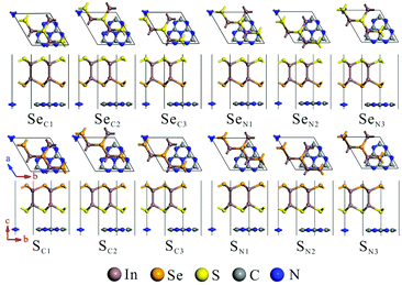 |
| | Fig. 1 Top and side views of the In2SeS/g-C3N4 heterostructure at different stacking patterns: SeC1, SeC2, SeC3, SeN1, SeN2, SeN3, SC1, SC2, SC3, SN1, SN2 and SN3. | |
Table 1 Interlayer spacing and binding energy of the In2Se/g-C3N4 heterostructure
| Type |
In2SeS/g-C3N4 |
| Stacking patterns |
SeC1 |
SeC2 |
SeC3 |
SeN1 |
SeN2 |
SeN3 |
|
E
b (eV) |
−2.161 |
−1.422 |
−2.044 |
−1.295 |
−1.505 |
−1.520 |
|
d
0 (Å) |
2.872 |
2.847 |
2.830 |
3.142 |
3.134 |
2.667 |
|
|
| Stacking patterns |
SC1 |
SC2 |
SC3 |
SN1 |
SN2 |
SN3 |
|
E
b (eV) |
−2.128 |
−2.108 |
−2.092 |
−2.210 |
−1.462 |
−1.948 |
|
d
0 (Å) |
2.731 |
2.783 |
2.781 |
2.848 |
3.041 |
3.042 |
3.2 Electronic properties of In2SeS/g-C3N4
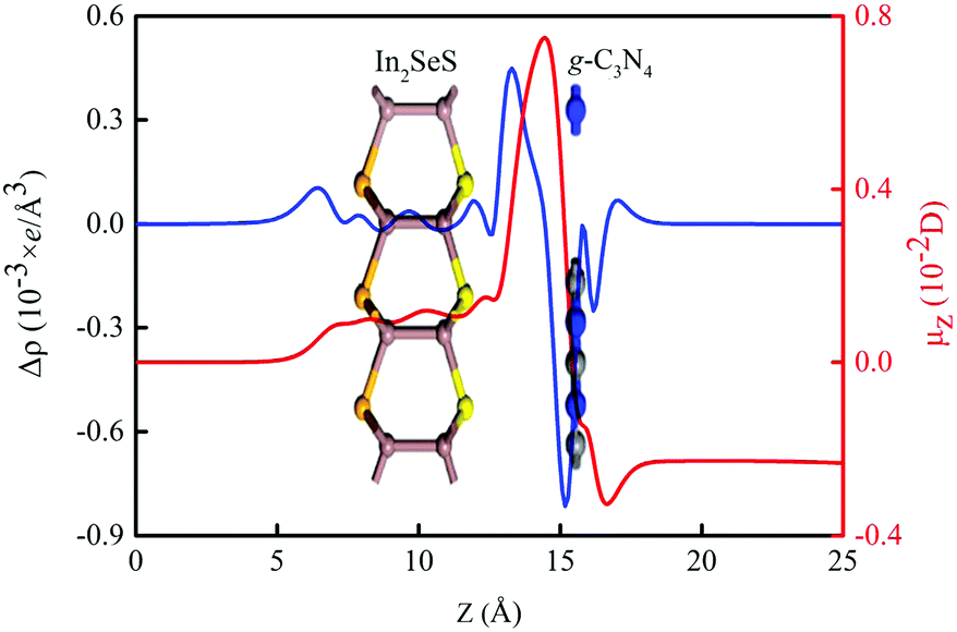
In order to investigate the electronic properties of the In2SeS/g-C3N4 heterostructure, the charge distribution and charge transfer are considered by analyzing the planar average charge density (ρ(z)) and the planar average charge density difference (Δρ(z)). Δρ(z) is given by the following formula:45| | | Δρ(z) = ρ(z)In2SeS/g-C3N4 − ρ(z)g-C3N4 − ρ(z)In2SeS | (2) |
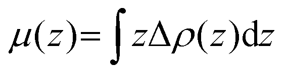
where ρ(z)In2SeS/g-C3N4, ρ(z)g-C3N4 and ρ(z)In2SeS are ρ(z) of the In2SeS/g-C3N4 heterostructure, g-C3N4 and monolayer In2SeS, respectively. In Fig. S3 (ESI†), ρ(z) values of g-C3N4, monolayer In2SeS and the In2SeS/g-C3N4 heterostructure are given. In Fig. 2, we can see that charges accumulate in the In2SeS layer and dissipates in the g-C3N4 layer, indicating that electrons are transferred from the g-C3N4 layer to the In2SeS layer. Thus the electrons and holes are effectively separated, which is conducive to the water splitting of the In2SeS/g-C3N4 heterostructure. To further study the interfacial electronic properties, the interface dipole moment μ(z) is also calculated using the following formula:45| |  | (3) |
A μ(z) of −0.23 D from the g-C3N4 layer to the In2SeS layer is found by calculation, confirming the formation of a heterostructure-induced interface dipole.
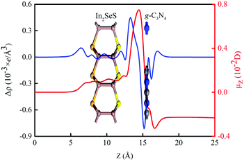 |
| | Fig. 2 Planar average charge density difference (blue line) and interfacial dipole moment (red line) along the Z-direction for the In2SeS/g-C3N4 heterostructure. | |
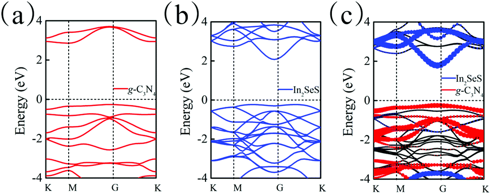
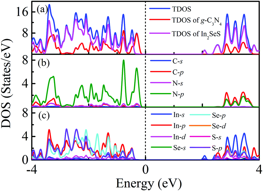
Moreover, the energy bands of g-C3N4, monolayer In2SeS and the In2SeS/g-C3N4 heterostructure are calculated, as shown in Fig. 3. Both g-C3N4 and monolayer In2SeS are indirect bandgap semiconductors with Eg values of 2.67 eV and 2.33 eV at the HSE06 level, respectively. Surprisingly, the In2SeS/g-C3N4 heterostructure is a direct bandgap semiconductor with an Eg of 2.03 eV, which is in the energy range of visible light (1.6–3.2 eV). Meanwhile, the top band of the valence band is mainly contributed by the g-C3N4 layer and the bottom band of the conduction band is mainly contributed by the In2SeS layer, which indicates that the electrons and holes are separated after the formation of the heterostructure and the In2SeS/g-C3N4 heterostructure is a type-II heterostructure. Meanwhile, the total density of states (TDOS) and the projected density of states (PDOS) for the In2SeS/g-C3N4 heterostructure are calculated. As shown in Fig. 4, the peak with the highest energy below the Fermi level is basically provided by the N–p orbit while the peak with the lowest energy above the Fermi level is basically provided by the In–s orbit, which implies that the positions of N and In atoms are better adsorption sites and also illustrates the separation of electrons and holes.
 |
| | Fig. 3 (a) Band structure of g-C3N4. (b) Band structure of monolayer In2SeS. (c) Band structure of the In2SeS/g-C3N4 heterostructure. | |
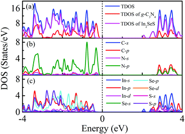 |
| | Fig. 4 (a) TDOS of the In2SeS/g-C3N4 heterostructure, PDOS of the g-C3N4 layer in the In2SeS/g-C3N4 heterostructure and PDOS of the In2SeS layer in the In2SeS/g-C3N4 heterostructure. (b) PDOS of C and N atoms in the g-C3N4 layer. (c) PDOS of In, Se and S atoms in the In2SeS layer. | |
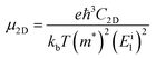
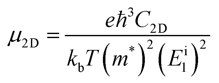
Furthermore, the carrier mobility (μ) of the In2SeS/g-C3N4 heterostructure is also calculated using the formula46–49
| |  | (4) |
where
e is the electron charge,
ℏ is Planck's constant divided by 2π and
kb is Boltzmann's constant.
T is the temperature, which is set to 298.15 K in our calculation to simulate room temperature.
m* is the effective mass of an electron or hole, which is calculated using the formula
| | 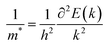 | (5) |
where
E is the total energy and
k is the wave vector. Then,
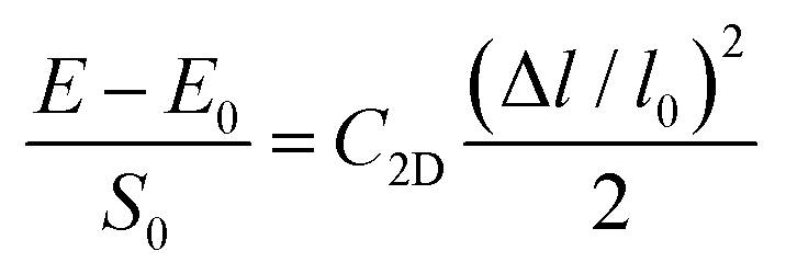
C2D is the 2D elastic modulus, which is calculated using the formula
| | 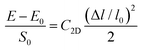 | (6) |
where
E and
E0 are the total energy of the crystal with and without deformation and
S0 is the lattice volume of the equilibrium state. Δ
l and
l0 are the variation of the lattice length and the initial lattice length, respectively. Then,
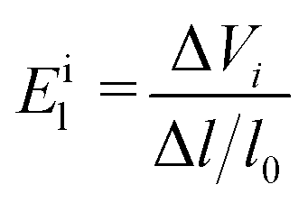
Eil is the deformation potential constant of the valence band maximum (VBM) for holes or the conduction band minimum (CBM) for electrons along the transport direction, which is calculated using the formula
| |  | (7) |
where Δ
Vi is the energy change of the
ith band under compression and tension. According to the above formula, the effective mass of the electrons and holes are 0.114
m0 and 1.36
m0, respectively. Energy changes of the In
2SeS/g-C
3N
4 heterostructure with strains in the
X-direction and the
Y-direction are given, as shown in Fig. S4 (ESI
†).
C2D values are both 87.89 J m
−2 along the
X-direction and the
Y-direction by calculation, and the electron and hole mobilities are 1665 cm
2 V
−1 s
−1 and 12 cm
2 V
−1 s
−1, respectively. The electron mobility is a relatively large value compared to other 2D materials, which is conducive to photocatalytic water splitting. Meanwhile, we have calculated the effective mass and carrier mobility of the In
2SeS/g-C
3N
4 heterostructure with a strain (from −3% to 3%) applied in the
X-direction and the
Y-direction, respectively, as shown in Table S2 (ESI
†). It is found that the strain has little effect on the carrier mobility of the In
2SeS/g-C
3N
4 heterostructure.
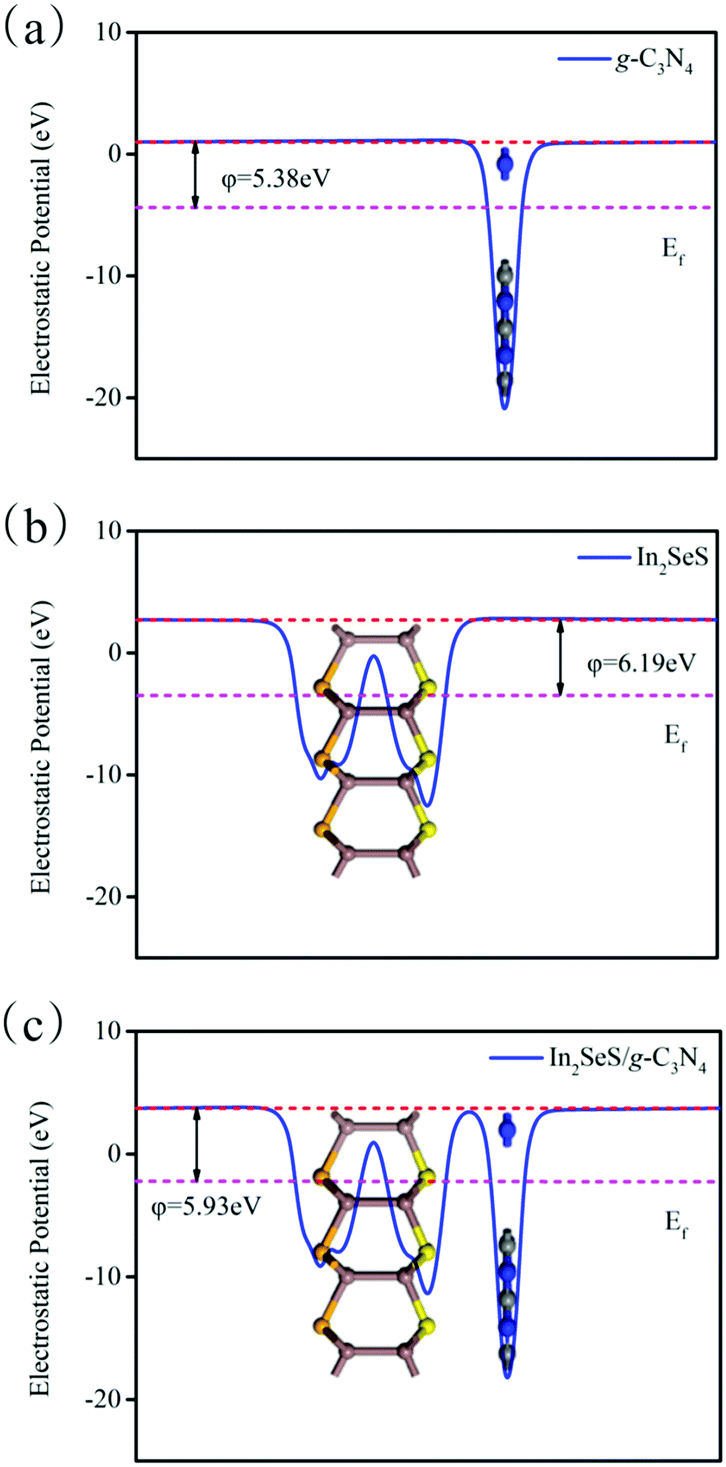
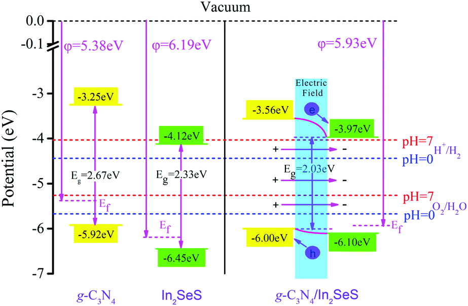
Then, the electrostatic potentials of g-C3N4, monolayer In2SeS and the In2SeS/g-C3N4 heterostructure are calculated. Moreover, their work function (φ) is also calculated, which is given by the formula
where
Evac is the electrostatic potential in a vacuum near to the surface.
Ef is the electrostatic potential at the Fermi level. As shown in
Fig. 5,
φ values of g-C
3N
4, monolayer In
2SeS and the In
2SeS/g-C
3N
4 heterostructure are 5.38 eV, 6.19 eV and 5.93 eV, respectively, which means that the g-C
3N
4 layer is easier to lose electrons than the In
2SeS layer. Moreover, the standard oxidation potential of O
2/H
2O can be calculated using
EO2/H2O = −5.67 eV + pH × 0.059 eV and the standard hydrogen potential of H
+/H
2 can be calculated using
EH+/H2 = −4.44 eV + pH × 0.059 eV.
50,51 To satisfy the requirements for photocatalytic water splitting, the potential of the CBM for photocatalysts should be higher than the standard hydrogen potential and the potential of the VBM for photocatalysts should be lower than the standard oxygen potential.
52 Therefore, based on the value of
φ, we have obtained the potentials at the Fermi level for g-C
3N
4, monolayer In
2SeS and the In
2SeS/g-C
3N
4 heterostructure. Their values are −5.38 eV, −6.19 eV and −5.93 eV, respectively. Then, based on the relative positions of the CBM, the VBM and the Fermi level (obtained according to
Fig. 3), we have calculated the potentials of band-edge positions for g-C
3N
4, monolayer In
2SeS and the In
2SeS/g-C
3N
4 heterostructure, as shown in
Fig. 6. The values of potential at CBM and at VBM for g-C
3N
4 are −3.25 eV and −5.92 eV, respectively. The values of potential at the CBM and at the VBM for monolayer In
2SeS are −4.12 eV and −6.45 eV, respectively. After the heterostructure is formed, the value of the potential at the CBM for the In
2SeS/g-C
3N
4 heterostructure is 3.97 eV, which is higher than the standard hydrogen potential (4.44 eV at pH = 0 and 4.01 eV at pH = 7). In addition, the value of the potential at the VBM for the In
2SeS/g-C
3N
4 heterostructure is 6.00 eV, which is lower than the standard oxygen potential (5.67 eV at pH = 0 and 5.26 eV at pH = 7). Therefore, in terms of potential, the In
2SeS/g-C
3N
4 heterostructure meets the requirements for photocatalytic water splitting. Part electrons are transferred from the g-C
3N
4 layer to the In
2SeS layer, which leads to the formation of an internal electric field from the g-C
3N
4 layer to the In
2SeS layer. The g-C
3N
4 layer is similar to the anode when electrolyzing water and the oxygen evolution reaction (OER) occurs. The In
2SeS layer is similar to the cathode of electrolyzing water and the hydrogen evolution reaction (HER) occurs.
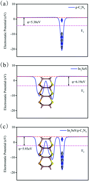 |
| | Fig. 5 (a) Electrostatic potential of g-C3N4. (b) Electrostatic potential of monolayer In2SeS. (c) Electrostatic potential of the In2SeS/g-C3N4 heterostructure. The red and pink dashed lines denote the Fermi level and the vacuum energy level, respectively. | |
 |
| | Fig. 6 Potential of band-edge positions for g-C3N4, monolayer In2SeS and the In2SeS/g-C3N4 heterostructure. | |
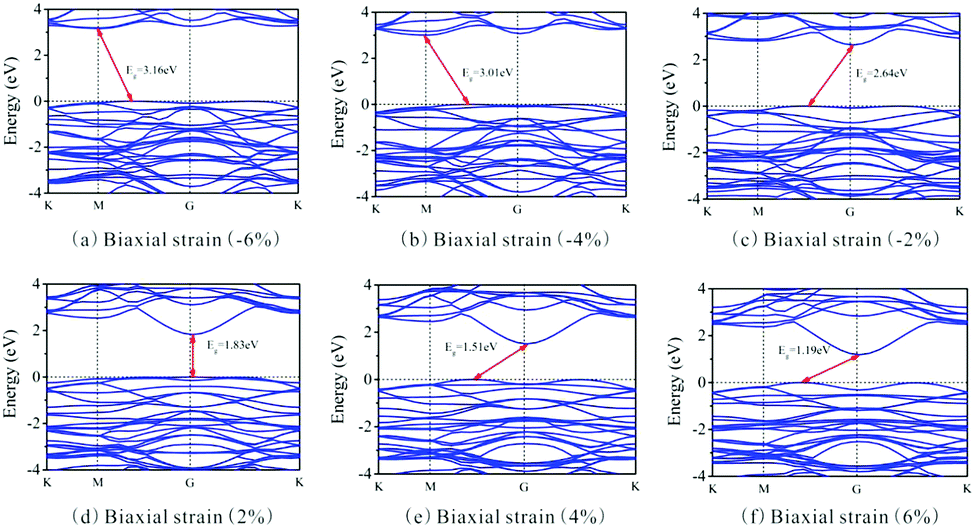
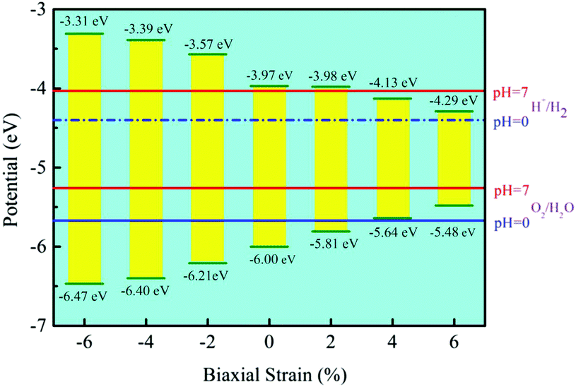
Besides, the In2SeS/g-C3N4 heterostructure is applied with biaxial strain. We find that the In2SeS/g-C3N4 heterostructure can withstand the biaxial strain from −6% to +6% without damaging its structure. As shown in Fig. 7, when the values of biaxial strain are −6%, −4%, −2%, 2%, 4% and 6%, the Eg values of the In2SeS/g-C3N4 heterostructure are 3.16 eV, 3.01 eV, 2.64 eV, 1.83 eV, 1.51 eV and 1.19 eV, respectively. It is concluded that Eg increases with the decrease of biaxial strain and Eg decreases with the increase of biaxial strain. Among them, when the value of biaxial strain is 2%, the In2SeS/g-C3N4 heterostructure is still a direct bandgap semiconductor. When the tensile stress is greater than 2% or compressive stress is applied, the In2SeS/g-C3N4 heterostructure will have a transition from a direct bandgap semiconductor to an indirect bandgap semiconductor. The potentials of band-edge positions under different biaxial strain conditions are shown in Fig. 8. When −6%, −4%, −2% and 2% biaxial strains are applied, the potentials of the VBM and the CBM still satisfy the requirements for photocatalytic water splitting. When 4% and 6% biaxial strains are applied, the potentials of the VBM and the CBM cannot satisfy the requirements for photocatalytic water splitting. It is noted that the larger the Eg of the heterostructure is, the greater the driving force for photocatalytic water splitting is. However, once Eg is too large, the energy required for electronic transition from the valence band to the conduction band increases and the wavelength range of sunlight that can provide sufficient energy reduces, which is not conducive to photocatalytic water splitting. Therefore, when −2% biaxial strain is applied, the effect of the In2SeS/g-C3N4 heterostructure for photocatalytic water splitting is the best in theory.
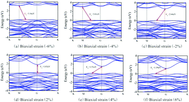 |
| | Fig. 7 Band structure under different biaxial strain conditions. | |
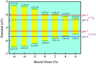 |
| | Fig. 8 Potential of band-edge positions under different biaxial strain conditions. | |
3.3 Optical properties of In2SeS/g-C3N4
In addition, the optical properties of the In2SeS/g-C3N4 heterostructure are predicted by using the GW+BSE approach. The real part (ε1) and the imaginary part (ε2) describe the dielectric properties and light-absorption ability of the material, respectively. The imaginary part (ε2) can be determined using the formula53–55| | 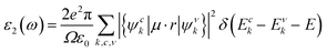 | (9) |
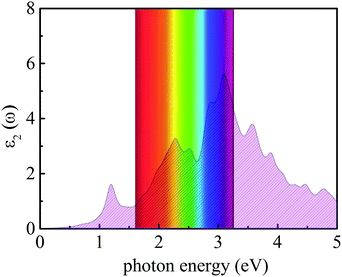
where ω represents the frequency of the electromagnetic radiation in energy units. Ω and ε0 represent the cell volume and the dielectric constant in free space, respectively. c and v represent the conduction and valence band states, respectively. u and r represent the vector defining the polarization of the incident electric field and the position vector, respectively. As shown in Fig. 9, the light-absorption ability of the In2SeS/g-C3N4 heterostructure is relatively strong. The highest light-absorption peak is between blue and purple light (corresponding to a photon energy of about 3 eV, and Eg of the In2SeS/g-C3N4 heterostructure is 2.03 eV), which indicates that after the In2SeS/g-C3N4 heterostructure absorbs the photons, there is enough energy to promote the electron to transit from the valence band to the conduction band.
 |
| | Fig. 9 Absorption spectrum of light. | |
3.4 Thermodynamic feasibility of the In2SeS/g-C3N4 heterostructure for photocatalytic water splitting
Finally, we have explored the thermodynamic feasibility of the In2SeS/g-C3N4 heterostructure for photocatalytic water splitting. The reaction of water splitting can be divided into two half reactions: the HER in the cathode and the OER in the anode. The reaction step of the HER is:28and the OER is divided into 4 small steps:56,57| | | H2O + * → OH* + H+ + e− | (11a) |
| | | OH* + H+ + e− → O* + 2(H+ + e−) | (11b) |
| | | O* + H2O + 2(H+ + e−) = OOH* + 3(H+ + e−) | (11c) |
| | | OOH* + 3(H+ + e−) = O2 + 4(H+ + e−) + * | (11d) |
where * indicates the In2SeS/g-C3N4 heterostructure substrate. OH*, O* and OOH* indicate that OH, O and OOH are adsorbed on the substrate, respectively. ΔG is calculated using the formula58,59| | | ΔG = ΔE + ΔZPE − TΔS − ΔGU − ΔGpH | (12) |
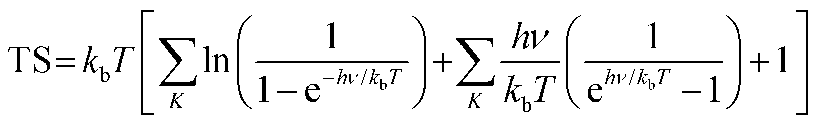
where ΔE represents the change in total energy. ΔZPE represents the change in zero point energy. ZPE could be calculated bywhere ν represents the vibrational frequency. Then, TΔS represents the change in entropic contributions (T is set to be 298.15 K). TS could be calculated by| |  | (14) |
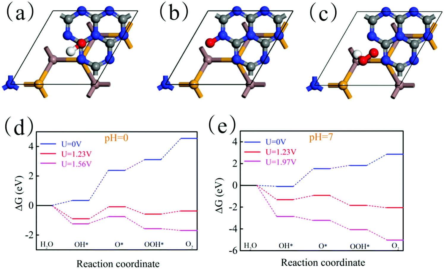
where e represents the electron charge, h represents Planck's constant and kb is Boltzmann's constant. Then, ΔGU represents the effect of electrochemical potential on ΔG, which is calculated by:where U represents the potential difference from the standard hydrogen electrode potential. Then, ΔGpH represents the effect of the pH value on ΔG, which is calculated by:Here, pH = 0 and pH = 7 are considered. Theoretically, the HER is relatively easy under the action of the potential and thus we only need to consider the feasibility of the OER in thermodynamics. Fig. 10(a)–(c) show the most stable adsorption site of OH, O and OOH on the g-C3N4 side of the In2SeS/g-C3N4 heterostructure, respectively. In Fig. 10(d), when pH = 0, U = 0 V, ΔG increases every step to 4.55 eV eventually. When pH = 0 and U = 1.23 V (minimum potential difference required for water splitting), ΔG declines in the first and third reactions while it increases in the second and fourth reactions. The actual electrochemical driving force of the OER is 1.56 eV at pH = 0 (potential difference between the potential of the VBM and the standard hydrogen potential). When pH = 0 and U = 1.56 V, ΔG declines in the first, third and fourth reactions while it increases in the second reaction. In all, when pH = 0, the existence of the increase of ΔG leads to the failure of water splitting for the In2SeS/g-C3N4 heterostructure in thermodynamics. In Fig. 10(e), when pH = 7 and U = 0 V, ΔG increases every step to 2.86 eV eventually. When pH = 7 and U = 1.23 V, ΔG declines in the first, third and fourth reactions while it increases in the second reaction. Therefore, when pH = 7, U = 0 or 1.23 eV, it is also impossible to split water for the In2SeS/g-C3N4 heterostructure in thermodynamics. The actual electrochemical driving force of the OER is 1.56 eV at pH = 7. When pH = 7 and U = 1.97 V, ΔG declines every step of the OER, which indicates that the In2SeS/g-C3N4 heterostructure for photocatalytic water splitting becomes feasible in thermodynamics under this condition.
 |
| | Fig. 10 (a)–(c) Optimized geometries of OH, O and OOH on the In2SeS/g-C3N4 heterostructure during OER. (d) The changes of Gibbs free energy at pH = 0 and at different potential differences (0 V, 1.23 V and 1.56 V). (e) The changes of Gibbs free energy at pH = 7 and at different potential differences (0 V, 1.23 V and 1.97 V). | |
IV Conclusions
Twelve structures of the In2SeS/g-C3N4 heterostructures are constructed according to different stacking patterns. Through the first-principles calculations, we find that the SN1 stacking pattern of the In2SeS/g-C3N4 heterostructure with a d0 of 3 Å is the most stable, and the In2SeS/g-C3N4 heterostructure is a typical type-II semiconductor with a direct bandgap of 2.03 eV, whose CBM and VBM are contributed by the In2SeS layer and the g-C3N4 layer, respectively. The potentials at the CBM and the VBM satisfy the requirements for photocatalytic water splitting. The electron mobility is 1665 cm2 V−1 s−1, which is a relatively large value compared to other 2D materials. Meanwhile, the In2SeS/g-C3N4 heterostructure has a strong ability to absorb light, mainly absorbing blue and purple light. In addition, when pH = 7 and U = 1.97 V, ΔG goes down every step of the OER, which verifies the feasibility of photocatalytic water splitting in thermodynamics. In short, the In2SeS/g-C3N4 heterostructure is expected to be a good candidate for photocatalytic water splitting.
Conflicts of interest
There are no conflicts to declare.
Acknowledgements
The authors acknowledge the support from the National Natural Science Foundation of China (NSFC, Grant No. 51471124, U1766216), the National Key R&D Program of China (2018YFB0905600) and the Natural Science Foundation of Shaanxi Province, China (2019JM-189, 2020JM-218).
Notes and references
- J. W. Ager and A. A. Lapkin, Science, 2018, 360, 707–708 CrossRef CAS PubMed.
- X. J. Huang, Q. B. Meng, H. Chen, X. L. Du and L. Q. Chen, Science, 2018, 360, 47–51 Search PubMed.
- Y. Zhou and Y. S. Liu, Nature, 2018, 560, 29 CrossRef CAS PubMed.
- S. G. Anton and A. E. A. Nucu, Renewable Energy, 2020, 147, 330–338 CrossRef.
- F. Gutierrez-Martin, A. B. Calcerrada, A. de Lucas-Consuegra and F. Dorado, Renewable Energy, 2020, 147, 639–649 CrossRef CAS.
- H. Mehrjerdi, A. Iqbal, E. Rakhshani and J. R. Torres, Energy Convers. Manage., 2019, 201, 11 CrossRef.
- H. Ishaq and I. Dincer, J. Cleaner Prod., 2020, 246, 12 CrossRef.
- C. J. Quarton, O. Tlili, L. Welder, C. Mansilla, H. Blanco, H. Heinrichs, J. Leaver, N. J. Samsatli, P. Lucchese, M. Robinius and S. Samsatli, Sustainable Energy Fuels, 2020, 4, 80–95 RSC.
- M. Chauhan, K. Soni, P. E. Karthik, K. P. Reddy, C. S. Gopinath and S. Deka, J. Mater. Chem. A, 2019, 7, 6985–6994 RSC.
- Y. J. Wu, C. B. Cao, C. Qiao, Y. Wu, L. F. Yang and W. Younas, J. Mater. Chem. C, 2019, 7, 10613–10622 RSC.
- J. Z. Liu, Y. H. Li, X. D. Zhou, H. Jiang, H. G. Yang and C. Z. Li, J. Mater. Chem. A, 2020, 8, 17–26 RSC.
- J. Zhu, M. Sun, S. J. Liu, X. H. Liu, K. Hu and L. Wang, J. Mater. Chem. A, 2019, 7, 26975–26983 RSC.
- K. Maeda, K. Teramura, D. L. Lu, T. Takata, N. Saito, Y. Inoue and K. Domen, Nature, 2006, 440, 295 CrossRef CAS PubMed.
- F. F. Hu, L. Q. Tao, H. Y. Ye, X. D. Li and X. P. Chen, J. Mater. Chem. C, 2019, 7, 7104–7113 RSC.
- T. Hisatomi, J. Kubota and K. Domen, Chem. Soc. Rev., 2014, 43, 7520–7535 RSC.
- S. Cao, T. S. Chan, Y. R. Lu, X. H. Shi, B. Fu, Z. J. Wu, H. M. Li, K. Liu, S. Alzuabi, P. Cheng, M. Liu, T. Li, X. B. Chen and L. Y. Piao, Nano Energy, 2020, 67, 9 Search PubMed.
- Y. Li, Q. Q. Shen, R. F. Guan, J. B. Xue, X. G. Liu, H. S. Jia, B. S. Xu and Y. C. Wu, J. Mater. Chem. C, 2020, 8, 1025–1040 RSC.
- V. Etacheri, R. Roshan and V. Kumar, ACS Appl. Mater. Interfaces, 2012, 4, 2717–2725 CrossRef CAS PubMed.
- I. M. Szilagyi, B. Forizs, O. Rosseler, A. Szegedi, P. Nemeth, P. Kiraly, G. Tarkanyi, B. Vajna, K. Varga-Josepovits, K. Laszlo, A. L. Toth, P. Baranyai and M. Leskela, J. Catal., 2012, 294, 119–127 CrossRef CAS.
- X. F. Ning and G. X. Lu, Nanoscale, 2020, 12, 1213–1223 RSC.
- A. R. Amani-Ghadim, F. Khodam and M. S. S. Dorraji, J. Mater. Chem. A, 2019, 7, 11408–11422 RSC.
- A. Kudo and Y. Miseki, Chem. Soc. Rev., 2009, 38, 253–278 RSC.
- H. Y. Liu, C. L. Yang, M. S. Wang and X. G. Ma, Appl. Surf. Sci., 2020, 501, 7 Search PubMed.
- J. Q. Wen, J. Xie, X. B. Chen and X. Li, Appl. Surf. Sci., 2017, 391, 72–123 CrossRef CAS.
- S. W. Cao and J. G. Yu, J. Phys. Chem. Lett., 2014, 5, 2101–2107 CrossRef CAS PubMed.
- X. Y. Du, X. Bai, L. Xu, L. Yang and P. K. Jin, Chem. Eng. J., 2020, 384, 14 CrossRef.
- Y. H. Li, M. L. Gu, T. Shi, W. Cui, X. M. Zhang, F. Dong, J. S. Cheng, J. J. Fan and K. L. Lv, Appl. Catal., B, 2020, 262, 11 Search PubMed.
- S. Lin, X. X. Ye, X. M. Gao and J. Huang, J. Mol. Catal. A: Chem., 2015, 406, 137–144 CrossRef CAS.
- A. V. Bandura, D. D. Kuruch and R. A. Evarestov, Isr. J. Chem., 2017, 57, 490–500 CrossRef CAS.
- M. Isik and N. M. Gasanly, Mater. Sci. Semicond. Process., 2020, 107, 5 CrossRef.
- R. Q. Zhang, L. L. Zhang, Q. J. Zheng, P. F. Gao, J. Zhao and J. L. Yang, J. Phys. Chem. Lett., 2018, 9, 5419–5424 CrossRef CAS PubMed.
- X. Yan, C. S. Liu, C. Li, W. Z. Bao, S. J. Ding, D. W. Zhang and P. Zhou, Small, 2017, 13, 8 Search PubMed.
- L. J. Sham and W. Kohn, Phys. Rev., 1966, 145, 561–567 CrossRef CAS.
- G. Kresse and J. Furthmuller, Phys. Rev. B: Condens. Matter Mater. Phys., 1996, 54, 11169–11186 CrossRef CAS PubMed.
- G. R. Su, S. Yang, S. Li, C. J. Butch, S. N. Filimonov, J. C. Ren and W. Liu, J. Am. Chem. Soc., 2019, 141, 1628–1635 CrossRef CAS PubMed.
- J. P. Perdew, K. Burke and M. Ernzerhof, Phys. Rev. Lett., 1996, 77, 3865–3868 CrossRef CAS PubMed.
- J. Heyd, G. E. Scuseria and M. Ernzerhof, J. Chem. Phys., 2003, 118, 8207–8215 CrossRef CAS.
- P. Umari, G. Stenuit and S. Baroni, Phys. Rev. B: Condens. Matter Mater. Phys., 2009, 79, 4 CrossRef.
- P. Umari, G. Stenuit and S. Baroni, Phys. Rev. B: Condens. Matter Mater. Phys., 2010, 81, 5 CrossRef.
- E. E. Salpeter and H. A. Bethe, Phys. Rev., 1951, 84, 1232–1242 CrossRef.
- S. Grimme, J. Comput. Chem., 2006, 27, 1787–1799 CrossRef CAS PubMed.
- M. M. Dong, C. He and W. X. Zhang, J. Mater. Chem. C, 2017, 5, 3830–3837 RSC.
- M. Ganaie and M. Zulfequar, J. Alloys Compd., 2016, 687, 643–651 CrossRef CAS.
- C. He, J. H. Zhang, W. X. Zhang and T. T. Li, J. Phys. Chem. C, 2019, 123, 5157–5163 CrossRef CAS.
- C. He, J. H. Zhang, W. X. Zhang and T. T. Li, J. Phys. Chem. Lett., 2019, 10, 3122–3128 CrossRef CAS PubMed.
- S. Bruzzone and G. Fiori, Appl. Phys. Lett., 2011, 99, 3 CrossRef.
- S. Takagi, A. Toriumi, M. Iwase and H. Tango, IEEE Trans. Electron Devices, 1994, 41, 2357–2362 CrossRef CAS.
- G. Fiori and G. Iannaccone, Proc. IEEE, 2013, 101, 1653–1669 CAS.
- J. S. Qiao, X. H. Kong, Z. X. Hu, F. Yang and W. Ji, Nat. Commun., 2014, 5, 7 Search PubMed.
- H. L. L. Zhuang and R. G. Hennig, Chem. Mater., 2013, 25, 3232–3238 CrossRef CAS.
- H. C. Yang, J. J. Li, L. Yu, B. B. Huang, Y. D. Ma and Y. Dai, J. Mater. Chem. A, 2018, 6, 4161–4166 RSC.
- R. M. N. Yerga, M. C. A. Galvan, F. del Valle, J. A. V. de la Mano and J. L. G. Fierro, ChemSusChem, 2009, 2, 471–485 CrossRef PubMed.
- T. Low, A. S. Rodin, A. Carvalho, Y. J. Jiang, H. Wang, F. N. Xia and A. H. C. Neto, Phys. Rev. B: Condens. Matter Mater. Phys., 2014, 90, 5 Search PubMed.
- Y. N. Zhang, J. N. Yun, K. Y. Wang, X. H. Chen, Z. Yang, Z. Y. Zhang, J. F. Yan and W. Zhao, Comput. Mater. Sci., 2017, 136, 12–19 CrossRef CAS.
- J. N. Hilfiker, M. Stadermann, J. N. Sun, T. Tiwald, J. S. Hale, P. E. Miller and C. Aracne-Ruddle, Appl. Surf. Sci., 2017, 421, 508–512 CrossRef CAS.
- S. Kattel, P. Atanassov and B. Kiefer, Phys. Chem. Chem. Phys., 2013, 15, 148–153 RSC.
- J. Rossmeisl, Z. W. Qu, H. Zhu, G. J. Kroes and J. K. Norskov, J. Electroanal. Chem., 2007, 607, 83–89 CrossRef CAS.
- J. Rossmeisl, A. Logadottir and J. K. Norskov, Chem. Phys., 2005, 319, 178–184 CrossRef CAS.
- A. Valdes, Z. W. Qu, G. J. Kroes, J. Rossmeisl and J. K. Norskov, J. Phys. Chem. C, 2008, 112, 9872–9879 CrossRef CAS.
Footnote |
| † Electronic supplementary information (ESI) available. See DOI: 10.1039/d0tc00852d |
|
| This journal is © The Royal Society of Chemistry 2020 |

 a,
F. S.
Han
a,
J. H.
Zhang
a and
W. X.
Zhang
a,
F. S.
Han
a,
J. H.
Zhang
a and
W. X.
Zhang
 monolayer In2SeS supercell stacked in the vertical direction with a lattice mismatch of about 3%. According to the different stacking patterns of g-C3N4 and monolayer In2SeS, twelve different heterostructures are constructed, as shown in Fig. 1. When Se atoms are adjacent to the g-C3N4 layer and C or N atoms are located in the hexagonal ring center of the In2SeS layer, the heterostructures are labeled as SeC1, SeC2, SeC3, SeN1, SeN2 and SeN3. When S atoms are adjacent to the g-C3N4 layer and C or N atoms are located in the hexagonal ring center of the In2SeS layer, the heterostructures are labeled as SC1, SC2, SC3, SN1, SN2 and SN3. To check the stability of the structure, the binding energy (Eb) of the 12 heterostructures are calculated using the following formula:44
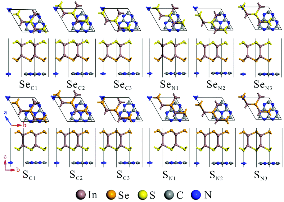


![[thin space (1/6-em)]](https://www.rsc.org/images/entities/char_2009.gif) T
T