
 Open Access Article
 This Open Access Article is licensed under a
 Creative Commons Attribution 3.0 Unported Licence
Examining charge transport networks in organic bulk heterojunction photovoltaic diodes using 1/f noise spectroscopy†
K.
Kaku
a,
A. T.
Williams
a,
B. G.
Mendis
b and
C.
Groves
*a
aSchool of Engineering and Computing Sciences, Durham University, South Road, Durham, DH1 3LE, UK. E-mail: chris.groves@durham.ac.uk
bPhysics Department, Durham University, South Road, Durham, DH1 3LE, UK
First published on 22nd May 2015
Abstract
In this article we present 1/f noise spectroscopy measurements relating to charge transport networks in poly(3-hexylthiophene) (P3HT):phenyl-C61-butyric acid methyl ester (PCBM) space-charge limited diode (SCLD) and organic photovoltaic (OPV) devices. The P3HT:PCBM active layer was varied to give a range of compositions and heterogeneities. The noise data obtained suggest that un-annealed P3HT:PCBM OPVs are limited by poor hole transport through the mixed phase, and that annealing promotes a more heterogeneous network, resulting in efficient charge transport through an increased population of P3HT crystallites, and better OPV performance. These findings are in agreement with literature studies for similar devices using other measurement techniques, demonstrating that 1/f noise is sensitive to the nature of the charge transport network in bipolar devices. Previous data only confirmed the sensitivity of 1/f noise spectroscopy to the charge transport network in unipolar devices, hence the current data suggest the technique can be used more generally to investigate charge transport networks in bulk heterojunction organic electronic devices such as OPVs and organic light-emitting diodes.
Introduction
The interest in organic photovoltaics (OPVs) is driven by the prospect of cheap, high-throughput manufacturing, enabled by the solution-processed active layer.1,2 OPVs commonly utilize a bulk heterojunction (BHJ) structure, in which nanoscale mixing of electron donating and electron accepting materials facilitates efficient charge generation.3,4 The properties of the BHJ morphology can have a significant impact on almost all aspects of OPV operation.5,6 For example, photoabsorption can be affected by ordering of the polymer donor,7,8 while the efficiency with which photogenerated excitons dissociate is determined by the availability of donor–acceptor interfaces.9,10 Charges created by dissociation of the charge transfer state may undergo geminate10,11 or non-geminate recombination12,13en route to collection at the contacts, both processes can again be strongly influenced by morphology. With the multitude of BHJ morphology-dependent processes that determine OPV performance, it can be a challenge to understand why an OPV operates in the manner it does. BHJ architectures are also used in a variety of other organic electronic devices. For example, solution-processed light-emitting diodes (OLEDs) utilise blends of conjugated polymers to tune efficiency and colour emission.14–16 Blends of semiconducting and insulating polymers are also increasingly being investigated as a way of improving the mechanical properties and stability of organic electronic devices.17 The relationship between BHJ morphology and device performance is therefore a common concern, and often involves a detailed investigation using a range of techniques to resolve.18A particular challenge is how to relate the BHJ morphology to the electrical performance, since even a thin film of a single material may display heterogeneous conduction,19,20 Techniques based upon atomic force microscopy (AFM)21–23 are useful in that they allow simultaneous measurement of local optical absorption, electronic and surface morphology information. However, AFM has better spatial sensitivity at the surface of the film,20 meaning the nature of charge conduction in the bulk is less well resolved, and furthermore requires careful measurement protocols to ensure devices do not degrade under measurement.21 Simple techniques that probe the charge transport network in the bulk may therefore accelerate understanding of how BHJ morphology influences performance in OPVs and other BHJ devices. In this paper we investigate the use of 1/f noise spectroscopy to characterise charge transport networks in such complex BHJ morphologies.
1/f noise is the electrical power associated with random current fluctuations present during device operation.24,25 These fluctuations are characterized by the power spectral density, SI(f), which is usually of the form 1/fα and measured below f = 1 kHz. 1/f noise spectroscopy was instrumental in diagnosing issues relating to charge transport during the early development of inorganic electronic devices,26–28 and is being used increasingly more often to characterise their organic counterparts.29–32 One reason for this is that the 1/f slope (i.e. α) provides information relating to the density of states (DoS),27,28 since a single trap state has α = 2 (i.e. a Lorentzian distribution) while a broader DoS has smaller values of α. In turn, the value of α can give qualitative information regarding trap-related degradation.30,33–35 However, of particular interest in this paper is the relationship between the percolation network, i.e. BHJ morphology, and 1/f noise. The magnitude of 1/f noise in a unipolar device scales as (p − pC)−κ, where p is the volume fraction of conducting material, pC is the percolation threshold, and κ is the dimensionality-dependent percolation exponent of noise.26,29,32 Early investigations on organic devices comprising blends of conducting and non-conducting polymers29,32 (i.e. unipolar devices) have shown that 1/f noise does indeed reveal detailed information about the charge transport network. In particular, Williams et al.29 showed that it is possible to discern between homogeneous and heterogeneous charge transport networks in poly(3-hexylthiophene) (P3HT):polystyrene (PS) blends by noise measurements alone.
In this paper we extend this work to examine the 1/f noise spectra and charge transport within bipolar P3HT:phenyl-C61-butyric acid methyl ester (PCBM) devices, being somewhat typical of the kinds of BHJ morphologies that can be obtained in OPV devices. Furthermore, P3HT:PCBM devices are a well-characterised system and so it is possible to compare the findings of noise spectroscopy with that of other experimental techniques. We vary both composition and annealing conditions to control the heterogeneity and percolation network. We investigate how sensitive noise spectroscopy is to changes in the conduction network in BHJ films by comparing transmission electron microscopy (TEM) imaging with noise spectroscopy, solar cell characteristics of OPV devices and current–voltage (J–V) characteristics of space-charge limited diodes (SCLDs). Our findings show that noise spectroscopy of P3HT:PCBM OPVs and SCLDs yield data that is consistent with previous investigations of charge transport even though the OPVs examined are bipolar devices. The agreement in the BHJ morphology suggested by 1/f noise spectroscopy and other measurements on this well-studied system is a key result, since this shows that 1/f noise has a broader applicability than for the exclusive study of unipolar devices.29 In particular, we show noise spectroscopy is sensitive to heterogeneity of the charge transport networks and can detect when OPV performance may be limited by the transport of one type of charge carrier. Given the low cost of equipment and the ease of measurement, this suggests that 1/f noise can find broad use in characterising charge transport in a wide range of technologically important bipolar BHJ devices.
Experimental
Materials
Regioregular P3HT (Electronic Grade; Mw = 50–70 kg mol−1), PCBM (99.5%) and poly(3,4-ethylenedioxythiophene): poly(styrenesulfonate) (PEDOT:PSS) were used as supplied from Reike Metals Inc., SunaTech Inc., and Clevios respectively.Device fabrication
OPVs and SCLDs were fabricated by first cleaning patterned ITO glass slides by sonication in acetone, propan-2-ol, Decon 90 solution (2% aqueous) and de-ionized water before subsequently being etched with O2 plasma (100 W for 5 min). PEDOT:PSS was immediately spin-coated onto the prepared ITO surface (2500 rpm for 45 s), followed by annealing at 180 °C for 2 min. P3HT and PCBM solutions were prepared using either 1,2-dichlorobenzene (DCB) or chloroform (CF) to promote more heterogeneous (i.e. more extensive phase separation, aggregation and/or crystallisation of components) or more homogenous (i.e. less extensive phase separation, aggregation or crystallisation of components) BHJ morphologies respectively. Hereafter devices fabricated using DCB and CF are referred to as heterogeneous and homogeneous, respectively.36 As an aside, we note that previous experimental studies using near-edge X-ray atomic fine structure (NEXAFS) on similar P3HT:PCBM devices suggest that the cathode interface is likely to be enriched with P3HT, and that different manufacture conditions may affect the surface composition.37,38 However, it has been shown that P3HT is a poor electron-blocking material.39 For these reasons we ascribe changes in noise performance between devices reported here to changes in the bulk rather than changes in the interface. We further note that all devices reported here have the same thickness (see ESI†) in order to try and maintain the relative importance of noise contributed by the bulk and the interface.For heterogeneous and homogeneous devices, P3HT and PCBM were separately dissolved in solvent and sonicated at a temperature of 45 °C for an hour. The solutions were then mixed and diluted to yield the desired P3HT:PCBM ratios, and stirred for a further 24 h at room temperature. The wt% of solutions was varied depending on the P3HT:PCBM ratio to produce ∼90 nm thick films for each composition; these are reported in Table S1 (ESI†). The active layer was spin coated (1000 rpm for 60 s) onto the pre-prepared PEDOT:PSS layer. Heterogeneous active layers were additionally annealed at 120 °C for 10 min.40 OPV devices or hole-only SCLDs were fabricated by evaporating 100 nm of Al or 50 nm of Au respectively onto the P3HT:PCBM active layer under vacuum and patterned using a mask (active area of 3.53 × 10⁻² cm2).
As an aside, note that we define Au-contact devices as hole-only diodes, and furthermore assume that hole conduction occurs primarily via the P3HT network. While we have not verified this independently, our reason for this assumption is based on the energy levels of the materials used. The workfunctions of Au and PEDOT:PSS are −5.1 eV![[thin space (1/6-em)]](https://www.rsc.org/images/entities/char_2009.gif) 44 and −5.3 eV45 respectively, while the HOMO levels of P3HT and PCBM are 5.1 eV and 6.3 eV respectively,46 and as such the hole injection barrier into PCBM is ∼1 eV larger than the corresponding barrier in P3HT. Similarly, since the LUMO of P3HT and PCBM is 4.5 eV and 4.0 eV, meaning the electron injection barrier is at least ∼0.6 eV larger than that for holes.
44 and −5.3 eV45 respectively, while the HOMO levels of P3HT and PCBM are 5.1 eV and 6.3 eV respectively,46 and as such the hole injection barrier into PCBM is ∼1 eV larger than the corresponding barrier in P3HT. Similarly, since the LUMO of P3HT and PCBM is 4.5 eV and 4.0 eV, meaning the electron injection barrier is at least ∼0.6 eV larger than that for holes.
All processing and measurement steps, with the exception of substrate preparation and PEDOT:PSS layer deposition, were carried out under a dry N2 environment. The volume ratio of P3HT in the film, pP3HT is calculated from the densities of P3HT (1.10 g cm−3)41,42 and PCBM (1.50 g cm−3).42,43 In this study, we examine P3HT:PCBM blend ratios corresponding to pP3HT = 0.41, 0.51, 0.63, 0.76, and 0.85.
Transmission electron microscopy
Transmission electron microscopy (TEM) measurements were performed to examine the morphology of the active layers.47 This was achieved by fabricating active layers in the same manner as above and immersing the sample into deionized water to float-off the P3HT:PCBM layer in order to transfer it onto a TEM grid. A JEOL 2100F FEG TEM was used for measuring TEM images under 200 kV operation mode using bright field contrast with defocus.47,48Noise spectroscopy
Noise spectroscopy measurements were carried out for a forward current of 1 mA. This current was chosen to ensure that the 1/f noise signal was large compared to the system background. We also note that a forward current of 1 mA is larger than would be anticipated under normal operating conditions for an OPV, however, we are using noise spectroscopy measurements to investigate the morphology of a real device, which is relevant to its normal operation, rather than probing normal operation of a real device itself. Current fluctuations were amplified using a low-noise current preamplifier (Stanford Research SR570), the output of which was sampled by a 24-bit data acquisition card (National Instruments NI-USB-4331). Resulting data was recorded and analysed using a LabView program. All measurements were carried out under dry N2 to minimise degradation of devices under test. Furthermore, electrical noise was minimised by biasing the devices under test using batteries, and enclosing the measurement within a grounded Faraday cage. Data presented here are representative of at least 5 devices for each blend composition. As an aside we note that it is possible that the background doping present in the current devices may vary due to solvent, and that this in turn may influence the effective shunt resistance. This in turn may affect Johnson noise, which is a white noise source. However, here we focus on the additive 1/f noise which dominates at low frequencies, and more importantly, the way in which this noise changes with pP3HT for a particular device type, and therefore particular solvent.Solar simulator and J–V characterisation
Current–voltage (J–V) measurements were performed in the dark and under dry N2 using a Source Measure Unit (SMU) (Keithley 2400). For solar simulator measurements, devices were illuminated through a mask by simulated AM 1.5 light from a class ABB solar simulator (Oriel Sol1A 94061A).Results and discussion
Morphology
Fig. 1 shows typical TEM images of active layers prepared to promote a heterogeneous morphology (a, c, e, and g) and a homogeneous morphology (b, d, f and h), for different blend ratios: (a) and (b) pP3HT = 0.41; (c) and (d) pP3HT = 0.51; (e) and (f) pP3HT = 0.63; (h) and (g) pP3HT = 0.85, respectively. The point resolution (∼8 nm) due to defocus makes it difficult to observe P3HT crystallization and pure P3HT domains (which appear as bright or dark regions in the TEM image48) smaller than 10 nm, particularly in the ∼90 nm thick films examined here. However, some coarser bright and dark regions can be seen in the image of heterogeneous active layers. Structure in the active layer is more difficult to discern in the homogeneous samples as expected. We ruled out the possibility of thickness variation causing the variation in TEM contrast by performing AFM measurements, which showed the active layers to have thickness differences of less than 3 nm over similar lateral length scales to that examined in TEM (Fig. S2, ESI†). Therefore, the contrast differences are more likely to show regions which comprise a greater proportion of crystalline P3HT regions or more aggregated PCBM regions for light and dark areas respectively. We stress that we cannot determine from the TEM images whether the morphology is 2-phase (i.e. some combination of pure P3HT and pure PCBM) or 3-phase (i.e. some combination of pure P3HT, pure PCBM and a mixed phase), or quantify the ‘amount’ of aggregated PCBM or crystallised P3HT within the film. That said, previous investigations indicate that the molecular weight of the P3HT used here (Mw = 50–70 kg mol−1) would lead to some proportion of amorphous P3HT:PCBM mixed phases in both heterogeneous and homogeneous blends,49 which would be expected to reduce contrast in TEM images. We note that these findings are in broad agreement with other investigations which show PCBM to be miscible in disordered P3HT.49–53 Nonetheless, we can confirm that the heterogeneous morphologies are both better phase separated and show more complex structure than the corresponding homogeneous morphologies at the same composition.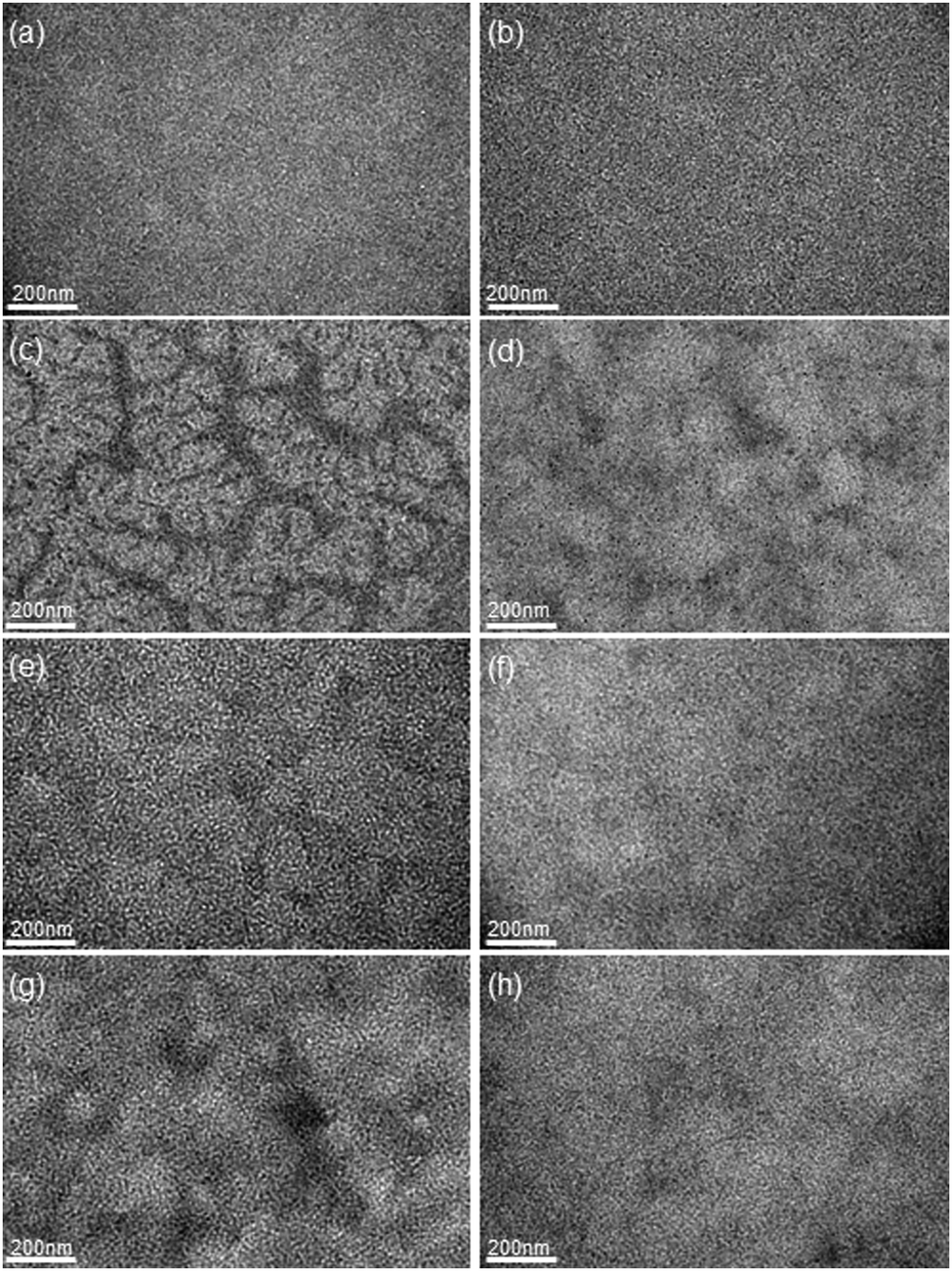 | ||
| Fig. 1 TEM images of the P3HT:PCBM blends: (a) and (b) pP3HT = 0.41, (c) and (d) pP3HT = 0.51, (e) and (f) pP3HT = 0.63, (g) and (h) pP3HT = 0.85; with thermal treatments: left column (a)–(g) corresponds to heterogeneous active layers, while right column (b)–(h) corresponds to homogeneous active layers. | ||
Space-charge limited diodes: DC characterisation
We begin by considering hole-only SCLDs fabricated with heterogeneous and homogeneous morphologies with a range of compositions (pP3HT). Fig. 2a and b shows J–V characteristics of the hole-only P3HT:PCBM diodes under dark conditions for homogenous and heterogeneous active layers respectively. As expected, increasing the relative volume fraction of P3HT increases the hole current for both active layers.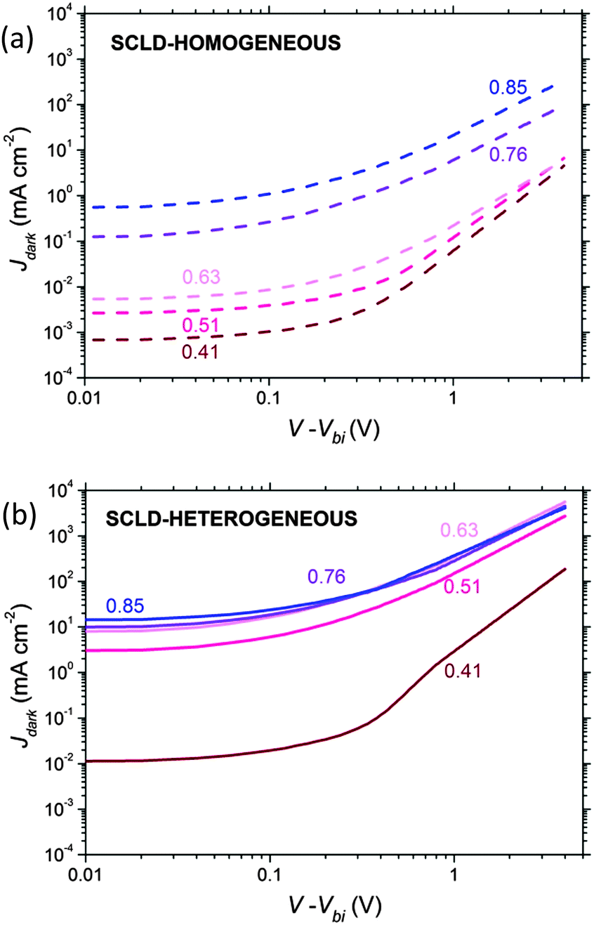 | ||
| Fig. 2 J–V characteristics under dark conditions for hole-only SCL P3HT:PCBM diodes for (a) homogeneous and (b) heterogeneous active layers, and blend ratios: pP3HT = 0.41 (brown), 0.51 (red), 0.63 (pink), 0.76 (purple) and 0.85 (blue). | ||
From these data we estimated the hole mobility μh using the following eqn (1) below,54
 | (1) |
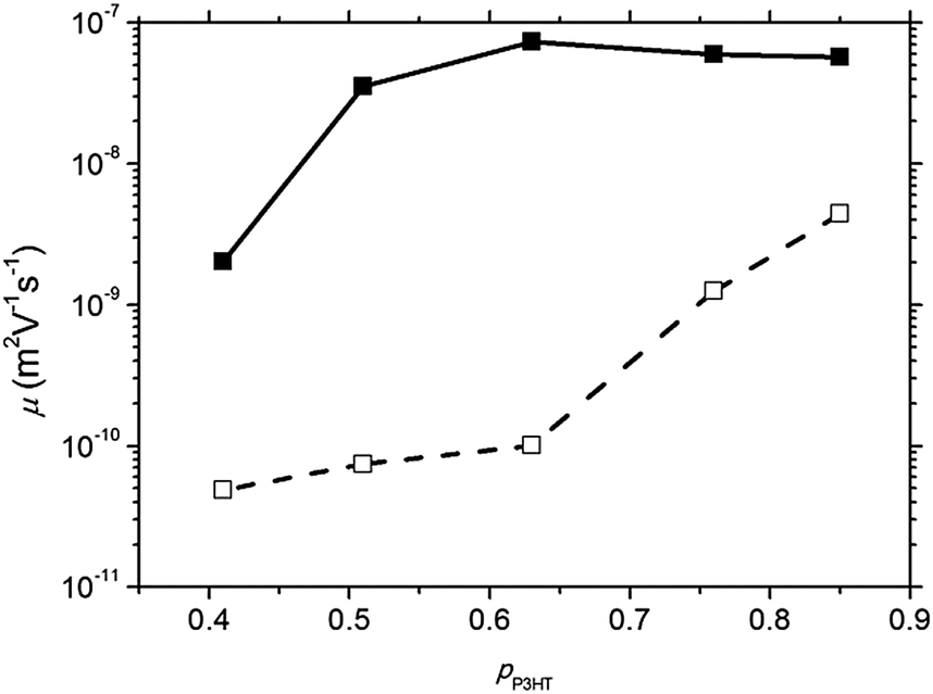 | ||
| Fig. 3 Hole mobility in the P3HT:PCBM blends as a function of P3HT volume percentage (pP3HT) for heterogeneous (solid line) and homogenous (dashed line) morphologies. | ||
Heterogeneous diodes (which used DCB as a solvent and were thermally annealed) exhibit a hole mobility which is ∼3 orders of magnitude larger than the corresponding homogeneous diodes (which used CF as a solvent and were not annealed) over the composition range examined, in agreement with other investigations on similar devices.58 It is notable that heterogeneous diodes can tolerate a lower P3HT content (pP3HT) without adversely affecting hole transport, with mobility only beginning to decline when pP3HT reduces below 0.5. This contrasts with homogeneous diodes where reducing the P3HT content below pP3HT = 0.75 results in a gentle reduction of hole mobility. It is challenging to measure a percolation threshold pC from the data obtained since, by definition we cannot measure current at the percolation threshold, and the conductivity of the films appears to vary non-uniformly with pP3HT. In light of this, we estimate the percolation threshold by extrapolating to the composition corresponding to μh = 4 × 10⁻¹¹ m2 V−1 s−1, which is pP3HT ∼ 0.40 for homogenous films and pP3HT ∼ 0.30 for heterogeneous films. This may suggest that morphologically heterogeneous films display more electrically heterogeneous conduction than the homogeneous counterparts, since the percolation threshold is lower and the rate at which conduction ‘switches off’ close to the percolation threshold is sharper.32 That said, it is not possible to distinguish between a ‘general’ change in mobility with P3HT content (for example via increased crystallisation due to increased availability of P3HT chains or other mechanism59) and an apparent change in bulk mobility due to changing number of percolation routes through the film. We further note that our main observation, namely that the conductivity of the homogeneous devices varies more gradually with pP3HT than for the heterogeneous devices, can also be seen in Fig. 2 and so is not contingent on the approximate mobility analysis used. The nature of hole conduction in the SCLD diodes was examined further using noise analysis.
Space-charge limited diodes: noise characterisation
Noise spectra are presented in Fig. 4a and b for homogeneous and heterogeneous diodes. The 1/f noise characteristics in the homogeneous diodes were found to be similar for devices where pP3HT ≥ 0.76, suggesting that the hole-transport network was far from the percolation threshold. However, homogeneous blends with pP3HT < 0.76 show enhanced noise, indicating that hole-transport through the P3HT network is approaching the percolation threshold.26,29,32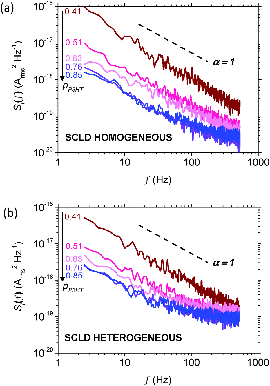 | ||
| Fig. 4 1/f noise spectra for (a) homogeneous and (b) heterogeneous P3HT:PCBM SCLDs with pP3HT = 0.41 (brown), 0.51 (red), 0.63 (pink), 0.76 (purple) and 0.85 (blue). | ||
The same is also true of the heterogeneous devices, namely that the noise spectra is insensitive to P3HT content above pP3HT = 0.76, and that below this value the noise value increases due to worsening percolation through the P3HT network, although here the increase is smaller than observed for the homogeneous diodes. We also note that the noise measured in heterogeneous diodes at high frequencies (f > 200 Hz) is greater than for homogeneous diodes. However, we will return to this later and first concentrate on the effect of pP3HT in both sets of devices.
It is expected that noise would scale with pP3HT in the manner (pP3HT − pC)−κ in this unipolar device, where κ is a constant related to the geometry and dimensionality of the percolation network.26,29,32Fig. 5 plots the noise power at f = 10 Hz as a function of (pP3HT − pC) for homogeneous and heterogeneous SCLDs. In order to do this we have performed fits to estimate the value of pC from the noise data, which were pC = 0.37 for heterogeneous SCLDs and pC = 0.39 for homogeneous SCLDs. These values are in good agreement with those obtained from analysis of the DC measurements shown in Fig. 2 and 3. The fitted κ values were 1.03 (±0.13 standard error) and 1.19 (±0.22 standard error) for the heterogeneous and homogeneous SCLDs respectively. While κ is an empirical measure of the percolation network, calculated values of κ for idealised lattices are smaller for 2D lattices (κ = 1.12) as compared to 3D lattices (κ = 1.56), and higher in general when disorder is introduced.32 The anticipated morphology in the SCLD devices examined here is almost certainly more complex than the idealised cases quoted, but nonetheless, the fitted value of κ qualitatively supports the picture of the hole-transport in heterogeneous SCLDs occurs via more constrained conduits than for homogeneous SCLDs. These findings are in accordance with conducting AFM measurements on similar annealed and non-annealed P3HT:PCBM films.60
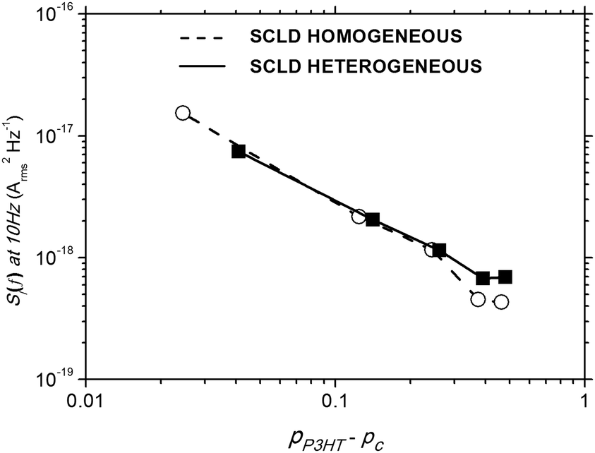 | ||
| Fig. 5 Noise power spectral density at 10 Hz as a function of (pP3HT − pC) for heterogeneous (solid) and homogeneous (open) SCLDs. | ||
Returning to Fig. 4, we note that the noise spectral power density is larger in the range f > 200 Hz for heterogeneous SCLDs than homogeneous SCLDs with the corresponding composition. As all diodes are biased at the same current, and charge transport is hole-only, this difference is not due to shot noise. We speculate that the increased noise in the region of 200–500 Hz for heterogeneous diodes is due to an increase in the proportion of crystalline P3HT after annealing. It has been shown that HOMO energies of amorphous and crystalline P3HT chains differ by ∼150 meV.61–64 Hence an increase in the proportion of crystalline regions may be expected to increase the width of the density of states (DoS) experienced by charges, since charges must traverse both crystalline and amorphous P3HT regions, and so broaden the ‘global average’ DoS width and leads to a smaller α.27 P3HT crystallization upon annealing or use of a high boiling point solvent is widely reported in the literature.5 The present TEM data (Fig. 1) places an upper bound on the size of any P3HT crystallites which may be present in our film, since we cannot observe any crystallites larger than ∼10 nm. However, the regions of light and dark contrast may indicate small P3HT crystallites in the heterogeneous films below the point resolution, which in turn could be the cause of the observed noise characteristics at high frequency.
Organic photovoltaic devices: DC characterisation
We now turn our attention to OPV devices, with active layers prepared as previously described for the SCLDs but with Al top contacts to allow injection and extraction of both carrier types. Fig. 6 shows J–V characteristics for typical devices. Homogeneous OPVs show inferior performance when compared to heterogeneous OPVs of similar composition, particularly in terms of short-circuit current (JSC) and fill-factor (FF), similar to that observed previously.5 The peak power conversion efficiency occurs for a lower P3HT content in the case of the heterogeneous OPV (pP3HT = 0.63) than for the homogeneous OPV (pP3HT = 0.85). These data may indicate that the heterogeneous OPV is less limited by hole transport than the homogeneous OPV, although we will return to this discussion later.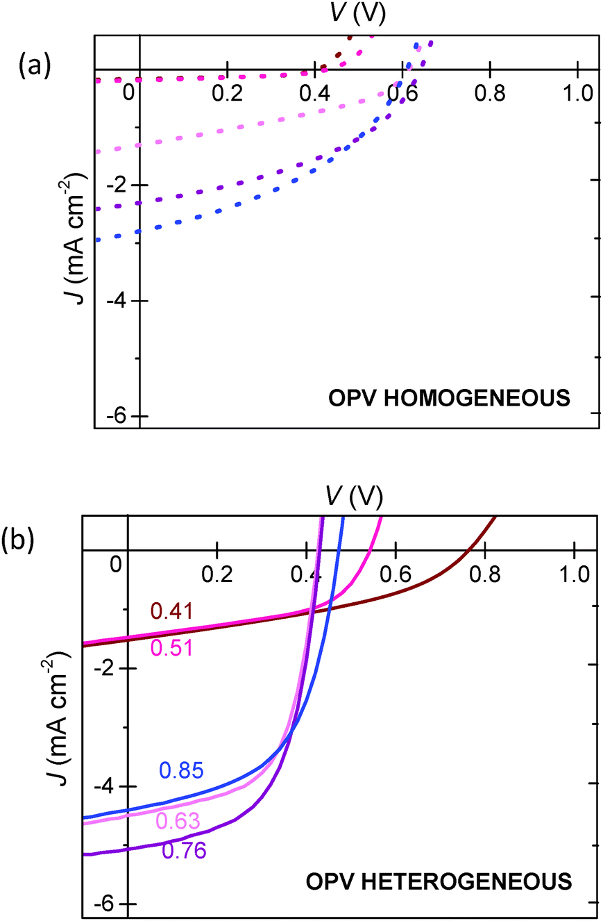 | ||
| Fig. 6 J–V characteristics of (a) homogeneous and (b) heterogeneous P3HT:PCBM OPVs under AM1.5 illumination with various blend ratios: pP3HT = 0.41 (brown), 0.51 (red), 0.63 (pink), 0.76 (purple) and 0.85 (blue). | ||
Organic photovoltaic devices: noise characterisation
Noise measurements were performed on P3HT:PCBM OPVs using the same procedure as for SCLDs above (note these measurements were in the dark), and shown in Fig. 7 below. The key difference between these data and those for SCLDs (Fig. 4) is that bipolar charge transport and recombination is possible in these devices. Although the noise spectra reveal an increase in noise for both morphologies when the P3HT content decreases from 0.85 to 0.41, the increase in noise is more striking for the homogeneous morphology. This difference in noise magnitude is highlighted in Fig. 8, which shows the noise power spectral density at f = 10 Hz over the range of P3HT compositions for both active layer types. It can be seen that noise power for homogeneous OPVs varies by more than an order of magnitude, while for heterogeneous OPVs, the noise varies by a factor of less than 3. Of course, in a bipolar device such as an OPV, the concept of a percolation threshold is not necessarily meaningful, since for low pP3HT it is possible for electron conduction pathways to carry the current through the device. Moreover there is the possibility of 1/f noise being introduced by trap-limited recombination.31 Nonetheless it is interesting to note that the noise characteristics of the homogeneous SCLDs and homogeneous OPVs are empirically similar. This contrasts to heterogeneous devices, where for the same forward current, the noise of SCLD devices is more sensitive to pP3HT than the OPV device.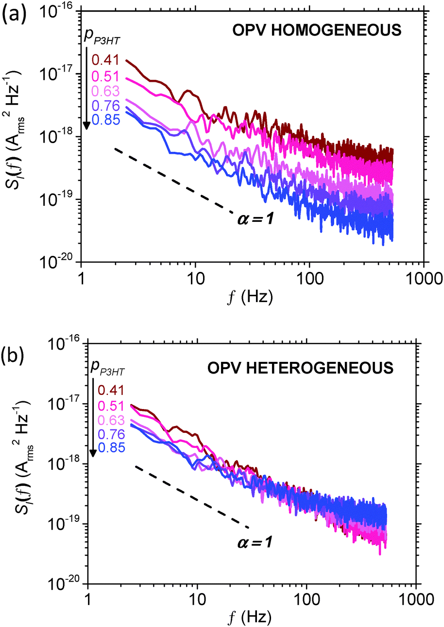 | ||
| Fig. 7 1/f noise spectra for (a) homogeneous and (b) heterogeneous P3HT:PCBM OPVs with various blend ratios: pP3HT = 0.41 (brown), 0.51 (red), 0.63 (pink), 0.76 (purple) and 0.85 (blue). | ||
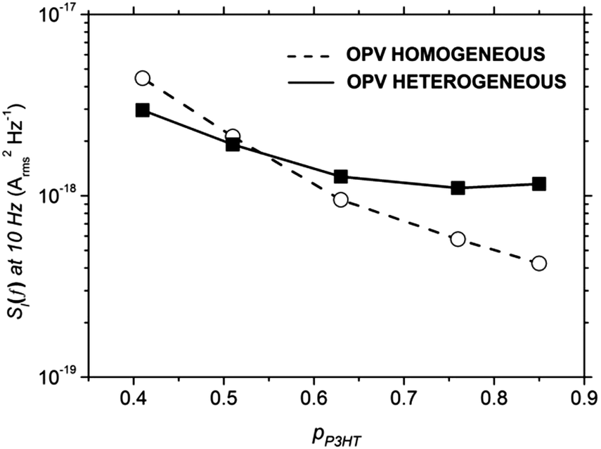 | ||
| Fig. 8 Noise spectral density measured at 10 Hz as a function of pP3HT. | ||
From these data we suggest the following interpretation. Charge transport of holes within the morphologically homogeneous P3HT:PCBM films is electrically homogeneous, with the majority of hole current passing through populous P3HT:PCBM mixed phases.49–53 This ‘featureless’ hole transport leads to a relatively high percolation threshold for holes, as evidenced by both the J–V (Fig. 2 and 3) and noise characteristics of SCLD devices (Fig. 4). This in turn impacts the performance of OPV devices, with optimum compositions favouring higher P3HT content (Fig. 6) due to hole-limited charge transport. This is reflected in the noise characteristics for homogeneous OPVs, with the noise power showing a strong dependence on P3HT content suggesting hole-limited charge transport (Fig. 8). This contrasts to heterogeneous P3HT:PCBM devices. The data for heterogeneous SCLD devices are consistent with electrically heterogeneous hole-transport, as evidenced by the lower percolation threshold (Fig. 2, 3 and 5) and weaker dependence of noise on P3HT content (Fig. 4 and 5). Electrically heterogeneous hole transport in annealed P3HT:PCBM films is consistent with conducting AFM measurements on similar devices.60 TEM images (Fig. 1) suggest greater phase separation, which may or may not include a population of P3HT crystallites below the ∼8 nm point resolution of the measurement, all of which is consistent with other investigations in which high boiling-point solvents or annealing was used.36,40,52,65 These data may indicate that hole transport in the heterogeneous films is primarily via the crystalline P3HT network rather than the residual amorphous P3HT:PCBM mixed phase. The more efficient nature of P3HT conduction is reflected in OPV devices, with peak performance occurring at a lower P3HT composition (Fig. 6). Noise measurements on heterogeneous OPV devices show only a very small dependence of noise power on P3HT content (Fig. 8). This, we speculate, is because charge transport in heterogeneous OPVs is not hole limited as is the case for homogeneous OPVs. Instead, the noise characteristics of heterogeneous OPVs probe the transition from electron-dominated transport for low pP3HT and hole-dominated transport for high pP3HT.
Of course we must recognise that charge transport is not the only factor determining OPV performance. In particular, the proportion of PCBM aggregates,64,66 polymer crystallites67,68 and mixed phases49,69 present within the film has been shown to lead to significant variations in charge generation efficiency for a variety of reasons.70 Indeed, some OPV systems have been shown to have almost morphology independent performance.71 Nonetheless, charge transport is intimately linked with the likelihood of non-geminate recombination,13 which in turn has been suggested to be performance limiting for a number of OPV systems, notably the P3HT:PCBM OPVs examined here.72 Further OPV systems continue to be investigated in which it is suggested that non-geminate recombination limits performance,73 and that further still, percolation of a particular type of charge is critical in determining performance.53 The current data suggest that noise analysis can be a helpful tool to examine in more detail the charge transport processes, which in turn influence device performance via non-geminate recombination.
Conclusions
1/f noise spectroscopy has been used to investigate hole-only and bipolar charge transport in P3HT:PCBM blends of varying composition and heterogeneity. Homogeneous devices were made using chloroform as a solvent, while heterogeneous devices were made using dicholorobenzene and were subsequently annealed. Analysis of noise data for hole-only SCLDs for a range of compositions suggested that hole transport occurred primarily through the amorphous P3HT:PCBM mixed phase in homogeneous films, while for heterogeneous films, hole transport occurred primarily through P3HT crystallites. Measurements on OPV devices found that optimum performance occurred for a higher P3HT content for homogeneous films than for heterogeneous films. Noise data on the same OPVs suggested that homogeneous films were limited by hole transport, while charge transport in heterogeneous OPVs was balanced, which is in agreement with both OPV device performance and noise analysis on SCLD devices. This morphological information inferred from 1/f noise measurements is in agreement with both TEM measurements on the same devices, and literature data on similar devices. In turn, this suggests that 1/f noise spectroscopy can be used to provide detailed information about charge transport networks in bipolar BHJ devices, extending the range of applicability demonstrated before only on unipolar devices.29 1/f noise measurements could therefore be used to examine charge transport networks in a range of technologically important devices, notably OPVs and OLEDs.Acknowledgements
This work was funded by the EPSRC, UK (grant reference EP/J009938/1). We thank Dr Chris Pearson for AFM thin-film thickness measurements.Notes and references
- J. Nelson, Mater. Today, 2011, 14, 462–470 CrossRef CAS.
- A. C. Arias, J. D. MacKenzie, I. McCulloch, J. Rivnay and A. Salleo, Chem. Rev., 2010, 110, 3–24 CrossRef CAS PubMed.
- J. J. M. Halls, C. A. Walsh, N. C. Greenham, E. A. Marseglia, R. H. Friend, S. C. Moratti and A. B. Holmes, Nature, 1995, 376, 498–500 CrossRef CAS PubMed.
- G. Yu, J. Gao, J. C. Hummelen, F. Wudl and A. J. Heeger, Science, 1995, 270, 1789–1791 CAS.
- C. J. Brabec, M. Heeney, I. McCulloch and J. Nelson, Chem. Soc. Rev., 2011, 40, 1185–1199 RSC.
- C. R. McNeill, Energy Environ. Sci., 2012, 5, 5653–5667 CAS.
- D. Chirvase, J. Parisi, J. C. Hummelen and V. Dyakonov, Nanotechnology, 2004, 15, 1317–1323 CrossRef CAS.
- G. Li, Y. Yao, H. Yang, V. Shrotriya, G. Yang and Y. Yang, Adv. Funct. Mater., 2007, 17, 1636–1644 CrossRef CAS PubMed.
- A. C. Arias, J. D. MacKenzie, R. Stevenson, J. J. M. Halls, M. Inbasekaran, E. P. Woo, D. Richards and R. H. Friend, Macromolecules, 2001, 34, 6005–6013 CrossRef CAS.
- C. R. McNeill, S. Westenhoff, C. Groves, R. H. Friend and N. C. Greenham, J. Phys. Chem. C, 2007, 111, 19153–19160 CAS.
- C. Groves, R. A. Marsh and N. C. Greenham, J. Chem. Phys., 2008, 129, 114903 CrossRef CAS PubMed.
- R. Hamilton, C. G. Shuttle, B. O’Regan, T. C. Hammant, J. Nelson and J. R. Durrant, J. Phys. Chem. Lett., 2010, 1, 1432–1436 CrossRef CAS.
- C. Groves and N. C. Greenham, Phys. Rev. B: Condens. Matter Mater. Phys., 2008, 78, 155205 CrossRef.
- H. Nishino, G. Yu, A. J. Heeger, T. A. Chen and R. D. Rieke, Synth. Met., 1995, 68, 243–247 CrossRef CAS.
- X. J. Zhang, D. M. Kale and S. A. Jenekhe, Macromolecules, 2002, 35, 382–393 CrossRef CAS.
- M. Berggren, O. Inganas, G. Gustafsson, J. Rasmusson, M. R. Andersson, T. Hjertberg and O. Wennerstrom, Nature, 1994, 372, 444–446 CrossRef CAS PubMed.
- A. D. Scaccabarozzi and N. Stingelin, J. Mater. Chem. A, 2014, 2, 10818–10824 CAS.
- R. Giridharagopal and D. S. Ginger, J. Phys. Chem. Lett., 2010, 1, 1160–1169 CrossRef CAS.
- J. J. M. van der Holst, M. A. Uijttewaal, R. Balasubramanian, R. Coehoorn, P. A. Bobbert, G. A. de Wijs and R. A. de Groot, Phys. Rev. B: Condens. Matter Mater. Phys., 2009, 79, 085203 CrossRef.
- O. G. Reid, K. Munechika and D. S. Ginger, Nano Lett., 2008, 8, 1602–1609 CrossRef CAS PubMed.
- L. S. C. Pingree, O. G. Reid and D. S. Ginger, Adv. Mater., 2009, 21, 19–28 CrossRef CAS PubMed.
- C. Groves, O. G. Reid and D. S. Ginger, Acc. Chem. Res., 2010, 43, 612–620 CrossRef CAS PubMed.
- R. Giridharagopal, G. E. Rayermann, G. Z. Shao, D. T. Moore, O. G. Reid, A. F. Tillack, D. J. Masiello and D. S. Ginger, Nano Lett., 2012, 12, 893–898 CrossRef CAS PubMed.
- J. Muller, ChemPhysChem, 2011, 12, 1222–1245 CrossRef PubMed.
- F. N. Hooge, IEEE Trans. Electron Devices, 1994, 41, 1926–1935 CrossRef CAS.
- S. Kogan, Electronic noise and fluctuations in solids, Cambridge University Press, 1996 Search PubMed.
- A. K. Raychaudhuri, Curr. Opin. Solid State Mater. Sci., 2002, 6, 67–85 CrossRef CAS.
- P. Dutta and P. M. Horn, Rev. Mod. Phys., 1981, 53, 497–516 CrossRef CAS.
- A. T. Williams, P. Farrar, A. J. Gallant, D. Atkinson and C. Groves, J. Mater. Chem. C, 2014, 2, 1742–1748 RSC.
- M. Bag, N. S. Vidhyadhiraja and K. S. Narayan, Appl. Phys. Lett., 2012, 101, 043903 CrossRef PubMed.
- L. Li, Y. Shen and J. C. Campbell, Sol. Energy Mater. Sol. Cells, 2014, 130, 151–155 CrossRef CAS PubMed.
- J. Planes and A. Francois, Phys. Rev. B: Condens. Matter Mater. Phys., 2004, 70, 184203 CrossRef.
- L. Ke, S. Bin Dolmanan, C. Vijila, S. J. Chua, Y. H. Han and T. Mei, IEEE Trans. Electron Devices, 2010, 57, 385–390 CrossRef CAS.
- L. Ke, S. Bin Dolmanan, L. Shen, C. Vijila, S. J. Chua, R. Q. Png, P. J. Chia, L. L. Chua and P. K. H. Ho, Appl. Phys. Lett., 2008, 93, 153507 CrossRef PubMed.
- M. Sampietro, G. Ferrari, D. Natali, U. Scherf, K. O. Annan, F. P. Wenzl and G. Leising, Appl. Phys. Lett., 2001, 78, 3262–3264 CrossRef CAS PubMed.
- S. T. Turner, P. Pingel, R. Steyrleuthner, E. J. W. Crossland, S. Ludwigs and D. Neher, Adv. Funct. Mater., 2011, 21, 4640–4652 CrossRef CAS PubMed.
- D. S. Germack, C. K. Chan, R. J. Kline, D. A. Fischer, D. J. Gundlach, M. F. Toney, L. J. Richter and D. M. DeLongchamp, Macromolecules, 2010, 43, 3828–3836 CrossRef CAS.
- A. F. Tillack, K. M. Noone, B. A. MacLeod, D. Nordlund, K. P. Nagle, J. A. Bradley, S. K. Hau, H. L. Yip, A. K. Y. Jen, G. T. Seidler and D. S. Ginger, ACS Appl. Mater. Interfaces, 2011, 3, 726–732 CAS.
- H. Wang, E. D. Gomez, J. Kim, Z. Guan, C. Jaye, D. A. Fischer, A. Kahn and Y.-L. Loo, Chem. Mater., 2011, 23, 2020–2023 CrossRef CAS.
- T. Agostinelli, S. Lilliu, J. G. Labram, M. Campoy-Quiles, M. Hampton, E. Pires, J. Rawle, O. Bikondoa, D. D. C. Bradley, T. D. Anthopoulos, J. Nelson and J. E. Macdonald, Adv. Funct. Mater., 2011, 21, 1701–1708 CrossRef CAS PubMed.
- T. J. Prosa, M. J. Winokur, J. Moulton, P. Smith and A. J. Heeger, Macromolecules, 1992, 25, 4364–4372 CrossRef CAS.
- S. B. Kirschner, N. P. Smith, K. A. Wepasnick, H. E. Katz, B. J. Kirby, J. A. Borchers and D. H. Reich, J. Mater. Chem., 2012, 22, 4364–4370 RSC.
- C. W. T. Bulle-Lieuwma, W. J. H. van Gennip, J. K. J. van Duren, P. Jonkheijm, R. A. J. Janssen and J. W. Niemantsverdriet, Appl. Surf. Sci., 2003, 203, 547–550 CrossRef.
- C. J. Brabec, A. Cravino, D. Meissner, N. S. Sariciftci, T. Fromherz, M. T. Rispens, L. Sanchez and J. C. Hummelen, Adv. Funct. Mater., 2001, 11, 374–380 CrossRef CAS.
- N. Koch, A. Vollmer and A. Elschner, Appl. Phys. Lett., 2007, 90, 043512 CrossRef PubMed.
- E. L. Ratcliff, B. Zacher and N. R. Armstrong, J. Phys. Chem. Lett., 2011, 2, 1337–1350 CrossRef CAS.
- B. G. Mendis, S. J. Bishop, C. Groves, M. Szablewski, A. Berlie and D. P. Halliday, Appl. Phys. Lett., 2013, 102, 253301 Search PubMed.
- S. S. van Bavel, E. Sourty, G. de With and J. Loos, Nano Lett., 2009, 9, 507–513 CrossRef CAS PubMed.
- P. Westacott, J. R. Tumbleston, S. Shoaee, S. Fearn, J. H. Bannock, J. B. Gilchrist, S. Heutz, J. deMello, M. Heeney, H. Ade, J. Durrant, D. S. McPhail and N. Stingelin, Energy Environ. Sci., 2013, 6, 2756–2764 CAS.
- D. R. Kozub, K. Vakhshouri, L. M. Orme, C. Wang, A. Hexemer and E. D. Gomez, Macromolecules, 2011, 44, 5722–5726 CrossRef CAS.
- N. D. Treat, M. A. Brady, G. Smith, M. F. Toney, E. J. Kramer, C. J. Hawker and M. L. Chabinyc, Adv. Energy Mater., 2011, 1, 145 CrossRef PubMed.
- W. Yin and M. Dadmun, ACS Nano, 2011, 5, 4756–4768 CrossRef CAS PubMed.
- J. A. Bartelt, Z. M. Beiley, E. T. Hoke, W. R. Mateker, J. D. Douglas, B. A. Collins, J. R. Tumbleston, K. R. Graham, A. Amassian, H. Ade, J. M. J. Frechet, M. F. Toney and M. D. McGehee, Adv. Energy Mater., 2013, 3, 364–374 CrossRef CAS PubMed.
- M. A. Lampert, Rep. Prog. Phys., 1964, 27, 329–367 CAS.
- W. F. Pasveer, J. Cottaar, C. Tanase, R. Coehoorn, P. A. Bobbert, P. W. M. Blom, D. M. de Leeuw and M. A. J. Michels, Phys. Rev. Lett., 2005, 94, 206601 CrossRef CAS.
- A. Armin, G. Juska, B. W. Philippa, P. L. Burn, P. Meredith, R. D. White and A. Pivrikas, Adv. Energy Mater., 2013, 3, 321–327 CrossRef CAS PubMed.
- Y. Zhang, B. de Boer and P. W. M. Blom, Adv. Funct. Mater., 2009, 19, 1901–1905 CrossRef CAS PubMed.
- V. D. Mihailetchi, H. X. Xie, B. de Boer, L. J. A. Koster and P. W. M. Blom, Adv. Funct. Mater., 2006, 16, 699–708 CrossRef CAS PubMed.
- P. W. M. Blom, V. D. Mihailetchi, L. J. A. Koster and D. E. Markov, Adv. Mater., 2007, 19, 1551–1566 CrossRef CAS PubMed.
- L. S. C. Pingree, O. G. Reid and D. S. Ginger, Nano Lett., 2009, 9, 2946–2952 CrossRef CAS PubMed.
- R. Noriega, J. Rivnay, K. Vandewal, F. P. V. Koch, N. Stingelin, P. Smith, M. F. Toney and A. Salleo, Nat. Mater., 2013, 12, 1038–1044 CrossRef CAS PubMed.
- Z. L. Guan, J. B. Kim, H. Wang, C. Jaye, D. A. Fischer, Y. L. Loo and A. Kahn, Org. Electron., 2010, 11, 1779–1785 CrossRef CAS PubMed.
- D. P. McMahon, D. L. Cheung and A. Troisi, J. Phys. Chem. Lett., 2011, 2, 2737–2741 CrossRef CAS.
- F. C. Jamieson, E. B. Domingo, T. McCarthy-Ward, M. Heeney, N. Stingelin and J. R. Durrant, Chem. Sci., 2012, 3, 485–492 RSC.
- X. N. Yang, J. Loos, S. C. Veenstra, W. J. H. Verhees, M. M. Wienk, J. M. Kroon, M. A. J. Michels and R. A. J. Janssen, Nano Lett., 2005, 5, 579–583 CrossRef CAS PubMed.
- C. Müller, T. A. M. Ferenczi, M. Campoy-Quiles, J. M. Frost, D. D. C. Bradley, P. Smith, N. Stingelin-Stutzmann and J. Nelson, Adv. Mater., 2008, 20, 3510–3515 CrossRef PubMed.
- A. M. Ballantyne, T. A. M. Ferenczi, M. Campoy-Quiles, T. M. Clarke, A. Maurano, K. H. Wong, W. Zhang, N. Stingelin-Stutzmann, J.-S. Kim, D. D. C. Bradley, J. R. Durrant, I. McCulloch, M. Heeney, J. Nelson, S. Tierney, W. Duffy, C. Mueller and P. Smith, Macromolecules, 2010, 43, 1169–1174 CrossRef CAS.
- O. G. Reid, J. A. N. Malik, G. Latini, S. Dayal, N. Kopidakis, C. Silva, N. Stingelin and G. Rumbles, J. Polym. Sci., Part B: Polym. Phys., 2011, 50, 27–37 CrossRef PubMed.
- B. A. Collins, J. R. Tumbleston and H. Ade, J. Phys. Chem. Lett., 2011, 2, 3135–3145 CrossRef CAS.
- C. Groves, Energy Environ. Sci., 2013, 6, 3202–3217 CAS.
- J. R. Tumbleston, A. C. Stuart, E. Gann, W. You and H. Ade, Adv. Funct. Mater., 2013, 23, 3463–3470 CrossRef CAS PubMed.
- C. G. Shuttle, B. O’Regan, A. M. Ballantyne, J. Nelson, D. D. C. Bradley and J. R. Durrant, Phys. Rev. B: Condens. Matter Mater. Phys., 2008, 78, 113201 CrossRef.
- G. F. A. Dibb, F. C. Jamieson, A. Maurano, J. Nelson and J. R. Durrant, J. Phys. Chem. Lett., 2013, 803–808 CrossRef CAS.
Footnote |
| † Electronic supplementary information (ESI) available: Solution concentrations and AFM scans, film thickness measurements. See DOI: 10.1039/c5tc00348b |
| This journal is © The Royal Society of Chemistry 2015 |