 Open Access Article
Creative Commons Attribution 3.0 Unported Licence
Covalent assembly of a two-dimensional molecular “sponge” on a Cu(111) surface: confined electronic surface states in open and closed pores†
Aneliia
Shchyrba
a,
Susanne C.
Martens
ab,
Christian
Wäckerlin‡
c,
Manfred
Matena
a,
Toni
Ivas
a,
Hubert
Wadepohl
b,
Meike
Stöhr
d,
Thomas A.
Jung
*c and
Lutz H.
Gade
*b
aDepartment of Physics, University of Basel, Klingelbergstrasse 82, 4056 Basel, Switzerland. E-mail: aneliia.shchyrba@unibas.ch
bAnorganisch-Chemisches Institut, Universität Heidelberg, Im Neuenheimer Feld 270, 69120 Heidelberg, Germany. E-mail: lutz.gade@uni-heidelberg.de
cLaboratory for Micro- and Nanotechnology, Paul Scherrer Institute, 5232 Villigen PSI, Switzerland. E-mail: thomas.jung@psi.ch
dZernike Institute for Advanced Materials, University of Groningen, Nijenborgh 4, 9747 AG Groningen, The Netherlands
First published on 4th June 2014
Abstract
We present a new class of on-surface covalent reactions, formed between diborylene-3,4,9,10-tetraaminoperylene and trimesic acid on Cu(111), which gives rise to a porous 2D-‘sponge’. This aperiodic network allowed the investigation of the dependence of electron confinement effects upon pore size, shape and even in partial confinement.
Covalent coupling reactions between molecular units adsorbed at surfaces have recently received increasing attention, in particular in the context of two-dimensional (2D) networks.1 The most established approaches include Ullman coupling,1a,b,d–f,2 Schiff base reaction,3 Glaser coupling,4 click-reaction5 or polyester condensation.6 The synthesis of covalently linked oligo- or polymeric structures is based on the coupling between planar polyfunctional building blocks which require a connectivity greater than two to form 2D assemblies. There are only a few examples of boron-based covalent chemistry to form aperiodic 2D networks.7
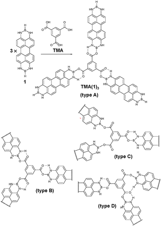
We previously reported the synthesis of N,N′;N′′,N′′′-diborylene-3,4,9,10-tetraaminoperylene derivatives (DIBOTAPs), which contain two borylene groups (BR) (Fig. 1).8 The parent compound (R = H) 1 was found to react readily with alcohols and carboxylic aids (R–OH), eliminating H2 and forming B–O–R bonds. This clean coupling along with the elimination of a gaseous co-product (H2) was thought to provide the basis for an on-surface synthesis of polymeric structures. In combination with a trifunctional carboxylic acid, such as trimesic acid (TMA), the linear DIBOTAP could couple to give a porous surface network. The relative angular flexibility of the C(O)–O–B junctions between the building blocks allows for the pore formation of variable size (and shape), resulting in a ‘sponge’-like covalent polymer.
 | ||
| Fig. 1 N,N′,N′′,N′′′-Diborylene-3,4,9,10-tetraaminoperylene (1) and benzene-1,3,5-tricarboxylic acid (TMA) on Cu(111) form TMA(1)3 by covalent reaction after thermal activation at ∼120 °C. The length of 1 is HB–BH 13.724 Å; B–B 11.433 Å and the width is H3–H9 6.564 Å; H2A–H8 6.570 Å (X-ray diffraction study in the ESI†). The flexibility of the covalent link formed by TMA deprotonation allows for a wide range of bonding geometries categorized as types A–D. | ||
Two-dimensional networks provide confinements for the scattering of electrons localized in the Shockley type surface state on noble metal (111) surfaces. Whereas the interaction with small scatterers (e.g. metal atoms) is well established,9 the scattering and confinement mechanisms for 2D molecular architectures10 are less understood. Therefore it is desirable to create a sample with coexisting pores of different size and shape, which are formed by the same polymer backbone. The investigation of the confined surface states in different open and closed pores by scanning tunnelling spectroscopy (STS) allows to draw conclusions regarding the size and shape dependence of the confinement effect.
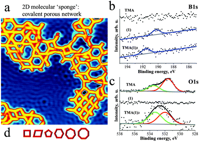
Deposition of 1 and then TMA on Cu(111) at room temperature (RT) and subsequent annealing at ∼120 °C resulted in the formation of porous networks (Fig. 2a, experimental details in ESI†). The pores of the network exhibited different shapes, as expected in view of the flexibility of the intermolecular joints discussed above. At least six different pore geometries could be identified as sketched in Fig. 2d (cf. Fig. S4, ESI†). Notably, the same type of network can also be formed under analogous preparation conditions on the less reactive Ag(111) substrate (cf. Fig. S5, ESI†).
 | ||
| Fig. 2 Deposition of TMA and 1 on Cu(111) at RT and subsequent annealing to 120 °C leads to the formation of an aperiodic covalent molecular network {TMA(1)3}. (a) STM micrograph taken at 5 K depicts pores of different size and shape (30 × 30 nm2). Scattering of surface state electrons leads to standing wave patterns on the substrate. (b) The XP spectra of TMA, 1 and TMA(1)3 reveal a significant shift (+1.35 eV) of the B1s peak towards higher binding energy and (c) the change of the ratio between O1s peaks upon the thermally activated formation of the covalent network. These observations strongly support the formation of a covalent O–B bond in the on-surface polymer, as sketched in Fig. 1. (d) Schematic representation of the various pore sizes and shapes. | ||
In order to determine the chemical integrity of the on-surface polymer we probed the chemical environment of C, N, O and B atoms of both TMA, 1 as well as of the {TMA(1)3} polymer by XPS (Fig. 2b and c). The C1s and N1s spectra are displayed in Fig. S2 (ESI†) and all XPS peak positions are summarized in Table S1 (ESI†). The unreacted compound 1 gives rise to N1s and B1s peaks at binding energy (BE) of 399.4 eV and 190.2 eV, respectively. For the native TMA molecule on Cu(111) two O1s peaks are observed at 531.6 eV and 533.5 eV. The signal at lower (higher) BE is assigned to oxygen in the carbonyl (hydroxyl) group. The observed ratio between the two oxygen species is different from 1![[thin space (1/6-em)]](https://www.rsc.org/images/entities/char_2009.gif) :
:![[thin space (1/6-em)]](https://www.rsc.org/images/entities/char_2009.gif) 1 due to partial deprotonation of the COOH-groups after TMA adsorbs on Cu(111).11 The on-surface {TMA(1)3} polymer is identified by a shift (+1.35 eV) of the B1s peak towards higher binding energy (Fig. 2b). This upshift is attributed to the significant difference in electronegativity between boron and oxygen leading to a partial positive charge on boron after formation of the O–B bond. Moreover, the O1s spectra clearly show a modified balance of the two oxygen species corresponding to C–O–B (533.3 eV) and C
1 due to partial deprotonation of the COOH-groups after TMA adsorbs on Cu(111).11 The on-surface {TMA(1)3} polymer is identified by a shift (+1.35 eV) of the B1s peak towards higher binding energy (Fig. 2b). This upshift is attributed to the significant difference in electronegativity between boron and oxygen leading to a partial positive charge on boron after formation of the O–B bond. Moreover, the O1s spectra clearly show a modified balance of the two oxygen species corresponding to C–O–B (533.3 eV) and C![[double bond, length as m-dash]](https://www.rsc.org/images/entities/char_e001.gif) O (532 eV) after polymerisation (Fig. 2c). The position of the N1s peak on the other hand remains unmodified (399.4 eV) (cf. Fig. S2, ESI†). Thus, the XPS analysis confirms the formation of an on-surface polymer based on covalent oxygen boron (O–B) bonds.
O (532 eV) after polymerisation (Fig. 2c). The position of the N1s peak on the other hand remains unmodified (399.4 eV) (cf. Fig. S2, ESI†). Thus, the XPS analysis confirms the formation of an on-surface polymer based on covalent oxygen boron (O–B) bonds.
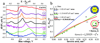
The 2D network acts as a system of different quantum wells interacting with the surface state electrons. Scattering at the ad-polymer can be clearly observed by the standing wave patterns in the STM data shown in Fig. 2a. For a further in-depth analysis of the quantum confinement effects we used scanning tunnelling spectroscopy (STS) at 5 K to probe the local (electronic) density of states (LDOS). The dI/dV spectrum, taken in the center of a certain pore, reveals a confined electronic surface state characterized by a peak energy dependent on the pore dimension (Fig. 3). Note that occupied and unoccupied states are probed at negative and positive sample bias voltage, respectively. The Cu(111) surface state is detected at −450 mV12 with respect to the Fermi level (EF) (red curve in Fig. 3a). The following peak values were measured by STS for the different sized and shaped pores: square −90 mV, parallelogram −180 mV, pentagon −265 mV, hexagon −336 mV, heptagon −360 mV and octagon −382 mV (Fig. 3a).
The pore confines the surface state electrons which are free in 2D on the extended Cu(111) substrate. In the following the energies E of the different confined states are referred to the onset of the native surface state E0. These energies E′ = E − E0 are known to scale linearly with the inverse area (1/A) as E′ = C/A with C = α1ℏ2π/(2m*)13 Here m* = 0.38 me12 is the effective electron mass (note, exact value of m* slightly deviates in literature, 0.41 me14) and α1 is a shape-dependent parameter for the first confined state. Thus, we plot E′ vs. 1/A (Fig. 3b). Since the shape-dependence for the first confined state is rather small (∼9% between square and circle), we employ here for a first approximation the value of a circular pore (α1 = 5.783).13 This yields a calculated slope Ccalc = 1.82 eV nm2 (Fig. 3b, dashed blue line) which does not agree well with the experimental data or its fitted slope Cfit = 1.15 eV nm2 (Fig. 3b, solid green line). Indeed, the effective area occupied by the confined surface state may deviate from the measured (from the center of the molecular backbones) area, as in case of surface states confined by monoatomic steps.9c Thus, we fit the data with an effective area which may be smaller or greater by a perimeter t (indicated in Fig. 3b). We find that if the slope C is kept fixed to the value of Ccalc this yields t = −0.30 nm, i.e. that the effective area extends by 0.3 nm beyond the molecular backbone. This result indicates that the barrier height is small enough to allow for a considerable penetration of the surface-state even beyond the center of the molecular backbone as observed earlier for a different porous network.10c
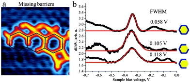
The “imperfections” of the pore structures in the 2D polymer sponge also allowed us to study the behaviour of the surface state electrons inside a partial confinement, i.e. inside “pores” with missing borders. In fact we observed significant electron confinement inside the hexagonal pores even if barriers are missing (Fig. 4). To the best of our knowledge such results have not been reported previously. Comparison of the STS peak-positions recorded in the centre of the closed hexagonal pore as well as in the centre of the pore with 1 and 2 missing barriers reveals the same position (∼−340 mV). By opening the barriers, however, a broadening of the STS peak (Fig. 4b) is evident, which we attribute to interference between partially confined and free 2D electrons. These findings suggest that the size of the pore plays an important role in defining the electronic characteristics of the quantum well state.
We have shown that the flexible covalent linkage formed upon coupling of DIBOTAP and TMA (liberating H2) allows for the formation of a nanoporous sponge-like 2D-network. The C–O–B bond formation, which gives rise to this surface network, was previously also found to occur in solution.8 The network forms pores of different architecture, in particular size, shape and symmetry which provides an interesting model system for the investigation of the confinement of Shockley type surface state electrons in a wide range of porous confinements. As expected, decreasing the surface area of the polygon shifts the confined state towards the Fermi level. Interestingly, this work provides further evidence that the confinement by polymer networks is not perfect. Furthermore, we analysed the confinement effects in open hexagonal pores with a varying number of absent side-walls or barriers. Notably, as shown here for the first time, the confined state energy remains identical to the intact pore. The removal of barriers leads to a broadening of the observed electronic quantum well state. Future work aims at employing modified building blocks to restrict the flexibility of the linker and thus to gain greater control of the porous on-surface architecture.
This work was supported by University of Heidelberg, the Doctoral College “Molekulare Sonden”, the National Centre of Competence in Research, “Nanoscience” (NCCR-Nano), Swiss Nanoscience Institute (SNI), Swiss National Science Foundation (grants No. 200020-137917, 206021-113149, 206021-121461), Foundation for Fundamental Research on Matter (FOM), part of the Netherlands Organisation for Scientific Research (NWO), NWO (Chemical Sciences, VIDI-grant No. 700.10.424) and the European Research Council (ERC-2012-StG 307760-SURFPRO).
Notes and references
- (a) T. Lin, X. S. Shang, J. Adisoejoso, P. N. Liu and N. Lin, J. Am. Chem. Soc., 2013, 135, 3576–3582 CrossRef CAS PubMed; (b) M. El Garah, J. M. MacLeod and F. Rosei, Surf. Sci., 2013, 613, 6–14 CrossRef CAS PubMed; (c) Y.-Q. Zhang, N. Kepčija, M. Kleinschrodt, K. Diller, S. Fischer, A. C. Papageorgiou, F. Allegretti, J. Björk, S. Klyatskaya, F. Klappenberger, M. Ruben and J. V. Barth, Nat. Commun., 2012, 3, 1286 CrossRef PubMed; (d) S. Schlögl, W. M. Heckl and M. Lackinger, Surf. Sci., 2012, 606, 999–1004 CrossRef PubMed; (e) L. Lafferentz, V. Eberhardt, C. Dri, C. Africh, G. Comelli, F. Esch, S. Hecht and L. Grill, Nat. Chem., 2012, 4, 215–220 CrossRef CAS PubMed; (f) M. Bieri, M.-T. Nguyen, O. Gröning, J. Cai, M. Treier, K. Aït-Mansour, P. Ruffieux, C. A. Pignedoli, D. Passerone, M. Kastler, K. Müllen and R. Fasel, J. Am. Chem. Soc., 2010, 132, 16669–16676 CrossRef CAS PubMed; (g) D. F. Perepichka and F. Rosei, Science, 2009, 323, 216–217 CrossRef CAS PubMed; (h) M. Matena, T. Riehm, M. Stöhr, T. A. Jung and L. H. Gade, Angew. Chem., Int. Ed., 2008, 47, 2414–2417 CrossRef CAS PubMed; (i) A. Gourdon, Angew. Chem., Int. Ed., 2008, 47, 6950–6953 CrossRef CAS PubMed.
- L. Grill, M. Dyer, L. Lafferentz, M. Persson, M. V. Peters and S. Hecht, Nat. Nanotechnol., 2007, 2, 687–691 CrossRef CAS PubMed.
- L. Xu, X. Zhou, Y. Yu, W. Q. Tian, J. Ma and S. Lei, ACS Nano, 2013, 7, 8066–8073 CrossRef CAS PubMed.
- H.-Y. Gao, H. Wagner, D. Zhong, J.-H. Franke, A. Studer and H. Fuchs, Angew. Chem., Int. Ed., 2013, 52, 4024–4028 CrossRef CAS PubMed.
- (a) P. Fesser, C. Iacovita, C. Wäckerlin, S. Vijayaraghavan, N. Ballav, K. Howes, J.-P. Gisselbrecht, M. Crobu, C. Boudon, M. Stöhr, T. A. Jung and F. Diederich, Chem. – Eur. J., 2011, 17, 5246–5250 CrossRef CAS PubMed; (b) F. Bebensee, C. Bombis, S.-R. Vadapoo, J. R. Cramer, F. Besenbacher, K. V. Gothelf and T. R. Linderoth, J. Am. Chem. Soc., 2013, 135, 2136–2139 CrossRef CAS PubMed; (c) O. Díaz Arado, H. Mönig, H. Wagner, J.-H. Franke, G. Langewisch, P. A. Held, A. Studer and H. Fuchs, ACS Nano, 2013, 7, 8509–8515 CrossRef PubMed.
- A. C. Marele, R. Mas-Ballesté, L. Terracciano, J. Rodríguez-Fernández, I. Berlanga, S. S. Alexandre, R. Otero, J. M. Gallego, F. Zamora and J. M. Gómez-Rodríguez, Chem. Commun., 2012, 48, 6779–6781 RSC.
- (a) N. A. A. Zwaneveld, R. Pawlak, M. Abel, D. Catalin, D. Gigmes, D. Bertin and L. Porte, J. Am. Chem. Soc., 2008, 130, 6678–6679 CrossRef CAS PubMed; (b) T. Faury, F. Dumur, S. Clair, M. Abel, L. Porte and D. Gigmes, CrystEngComm, 2013, 15, 2067–2075 RSC.
- T. Riehm, G. De Paoli, H. Wadepohl, L. De Cola and L. H. Gade, Chem. Commun., 2008, 5348–5350 RSC.
- (a) M. F. Crommie, C. P. Lutz and D. M. Eigler, Science, 1993, 262, 218–220 CAS; (b) K.-F. Braun and K.-H. Rieder, Phys. Rev. Lett., 2002, 88, 096801 CrossRef; (c) J. Li, W.-D. Schneider, R. Berndt and S. Crampin, Phys. Rev. Lett., 1998, 80, 3332–3335 CrossRef CAS.
- (a) P. Han and P. S. Weiss, Surf. Sci. Rep., 2012, 67, 19–81 CrossRef CAS PubMed; (b) L. Gross, F. Moresco, L. Savio, A. Gourdon, C. Joachim and K.-H. Rieder, Phys. Rev. Lett., 2004, 93, 056103 CrossRef; (c) J. Lobo-Checa, M. Matena, K. Müller, J. H. Dil, F. Meier, L. H. Gade, T. A. Jung and M. Stöhr, Science, 2009, 325, 300–303 CrossRef CAS PubMed; (d) F. Klappenberger, D. Kühne, W. Krenner, I. Silanes, A. Arnau, F. J. García de Abajo, S. Klyatskaya, M. Ruben and J. V. Barth, Nano Lett., 2009, 9, 3509–3514 CrossRef CAS PubMed; (e) F. Klappenberger, D. Kühne, W. Krenner, I. Silanes, A. Arnau, F. J. García de Abajo, S. Klyatskaya, M. Ruben and J. V. Barth, Phys. Rev. Lett., 2011, 106, 026802 CrossRef CAS; (f) R. Stiufiuc, L. M. A. Perdigão, B. Grandidier, D. Deresmes, G. Allan, C. Delerue, D. Stiévenard, P. H. Beton, S. C. Erwin, M. Sassi, V. Oison and J.-M. Debierre, Phys. Rev. B, 2010, 81, 045421 CrossRef; (g) S. Wang, W. Wang, L. Z. Tan, X. G. Li, Z. Shi, G. Kuang, P. N. Liu, S. G. Louie and N. Lin, Phys. Rev. B, 2013, 88, 245430 CrossRef.
- (a) S. Stepanow, T. Strunskus, M. Lingenfelder, A. Dmitriev, H. Spillmann, N. Lin, J. V. Barth, C. Wöll and K. Kern, J. Phys. Chem. B, 2004, 108, 19392–19397 CrossRef CAS; (b) J. V. Barth, J. Weckesser, N. Lin, A. Dmitriev and K. Kern, Appl. Phys. A: Mater. Sci. Process., 2003, 76, 645–652 CrossRef CAS PubMed.
- M. F. Crommie, C. P. Lutz and D. M. Eigler, Nature, 1993, 363, 524–527 CrossRef CAS.
- E. Lijnen, L. Chibotaru and A. Ceulemans, Phys. Rev. E, 2008, 77, 016702 CrossRef.
- F. Reinert, G. Nicolay, S. Schmidt, D. Ehm and S. Hüfner, Phys. Rev. B, 2001, 63, 115415 CrossRef.
Footnotes |
| † Electronic supplementary information (ESI) available: Experimental details, additional XPS and STM data. Data of the X-ray diffraction study of 1 (CIF format). CCDC 988044. For ESI and crystallographic data in CIF or other electronic format see DOI: 10.1039/c4cc02463j |
| ‡ Present address: Institute of Condensed Matter Physics, Ecole Polytechnique Fédérale de Lausanne, 1015 Lausanne, Switzerland. |
| This journal is © The Royal Society of Chemistry 2014 |


