
 Open Access Article
 This Open Access Article is licensed under a Creative Commons Attribution-Non Commercial 3.0 Unported Licence
Printed, cost-effective and stable poly(3-hexylthiophene) electrolyte-gated field-effect transistors†
Davide
Blasi
 a,
Fabrizio
Viola
b,
Francesco
Modena
bc,
Axel
Luukkonen
d,
Eleonora
Macchia
ad,
Rosaria Anna
Picca
ae,
Zahra
Gounani
d,
Amit
Tewari
d,
Ronald
Österbacka
d,
Mario
Caironi
b,
Zsolt M.
Kovacs Vajna
f,
Gaetano
Scamarcio
g,
Fabrizio
Torricelli
*f and
Luisa
Torsi
*ade
a,
Fabrizio
Viola
b,
Francesco
Modena
bc,
Axel
Luukkonen
d,
Eleonora
Macchia
ad,
Rosaria Anna
Picca
ae,
Zahra
Gounani
d,
Amit
Tewari
d,
Ronald
Österbacka
d,
Mario
Caironi
b,
Zsolt M.
Kovacs Vajna
f,
Gaetano
Scamarcio
g,
Fabrizio
Torricelli
*f and
Luisa
Torsi
*ade
aCSGI (Centre for Colloid and Surface Science), 70125 Bari, Italy. E-mail: luisa.torsi@uniba.it
bCenter for Nano Science and Technology@PoliMi, Istituto Italiano di Tecnologia, via G. Pascoli 70/3, 20133 Milan, Italy
cDipartimento di Elettronica, Infomazione e Bioingegneria, Politecnico di Milano - Milano, Italy
dFaculty of Science and Engineering, Åbo Akademi University, 20500 Turku, Finland
eDipartimento di Chimica, Università degli Studi di Bari “Aldo Moro”, 70125 Bari, Italy
fDipartimento Ingegneria dell’Informazione, Università degli Studi di Brescia, via Branze 38, 25123 Brescia, Italy. E-mail: fabrizio.torricelli@unibs.it
gDipartimento Interateneo di Fisica “M. Merlin”, Università degli Studi di Bari “Aldo Moro”, 70125 Bari, Italy
First published on 2nd September 2020
Abstract
Organic bioelectronic sensors based on an electrolyte gated field-effect transistor are gaining momentum due to their extraordinary high-performance level that enables label-free selective single-molecule detection of both genomic and protein biomarkers with a millimeter-wide electrolyte-gated field-effect transistor (EGOFET) device. The organic semiconductor channel material used so far is a spin-coated regio-regular poly(3-hexylthiophene) (P3HT). Of paramount importance is to design an EGOFET sensor that is stable and cost-effective. To address the latter feature, an ink-jet printed regio-regular P3HT film is here investigated as the channel material. Moreover, the EGOFET device structure is intended to comprise a coplanar lateral gate electrode that enables mechanical and electrical stability. Overall, the structure is compatible with large area processing so it can be fabricated at low-costs and can be operated continuously for eight days. Additionally, systematic optical and Raman characterization of the P3HT film proves that the printing process results in a film with a low energetic disorder (better π–π stacking in the crystalline regions) that likely enables stable operation. However, the higher quality crystalline regions (as compared to a spin-coated film) are dispersed in a more significant fraction of the amorphous disordered material with a larger amount of trap states. The higher crystalline order is ascribed to the higher boiling point and slower evaporation of the ortho-dichlorobenzene solvent used in the printing process. Overall, the present study provides a systematic insight into the structure–property correlations, essential to design a well-functioning and cost-effective EGOFET for high-performance electronic biosensing. It also provides one of the few investigations comparing the features characterizing a spin-coated and an ink-jet printed P3HT film.
Introduction
Poly(3-hexylthiophene) (P3HT) is one of the most studied polymeric semiconductors and has been successfully used in a wide range of applications spanning from organic field-effect transistors (OFETs),1–4 solar cells5 and biosensors.6 P3HT solubility conveniently enables the deposition to be carried out from solution processing. However, while most studies concern devices based on a spin-coated P3HT film, fewer address a P3HT film deposited by printing. The latter deposition technique offers the advantage of being readily compatible with large-area cost-effective manufacturing protocols. Further on, very few works7 propose a systematic comparison of structure–performance correlations of spin-coated and printed P3HT films.Morphological and structural characterization shows that a solution-processed regio-regular P3HT film is polycrystalline in nature exhibiting an alternation of crystalline domains separated by amorphous grain boundaries.8 In this latter phase, charge traps are present, hindering a number of carriers that would be free in an ideal perfectly crystalline material, thereby decreasing the mobility. Indeed, traps are localized intra-gap states. Hence, the structural order of molecules in semiconducting polymeric materials can significantly impact on their optical and electronic properties. As an instance, films of regio-regular P3HT, exhibiting a high degree of molecular order (π–π stacking of molecules),9 can show an increase in absorption at longer wavelength and an increase in charge carrier mobility as compared to its disordered form.10 Hence, an independent assessment of the molecular order is important to establish useful structure–property relationship. Indeed, the optical properties of P3HT in the solid state are well-characterized so they can be used to assess the supramolecular structure of the film.11–14 To this end UV-Vis but also Raman characterization of P3HT can be used to establish correlations between the optical and electronic performance level of the film and its structure. These pieces of information can be eventually used to optimize the film processing conditions.
Lately, electrolyte gated field-effect transistors (EGOFETs) have attracted a great deal of interest for their possible application in the growing field of printed electronics.15 The main peculiarity of an EGOFET consists in engaging an electronic insulating and ionic conducting electrolyte (e.g. water), acting as the dielectric that couples the transistor channel with the gate electrode. A detailed description of the operational mechanisms of EGOFETs involving source–drain current modulation via gating of the semiconducting channel by means of high capacitance electrical-double-layers (EDLs), installed at the gate/electrolyte and electrolyte/P3HT interfaces, is provided elsewhere.15,16 Here, it is just worth mentioning that the hydrophobic nature of regio-regular P3HT operated in water makes it an ideal material to seal the EDL at the water/P3HT interfaces into a two-dimensional structure. P3HT EGOFETs serve, hence, a prototypical example of 2D field-effect transistors operated in a water environment.16
The possibility to operate a FET in water has opened a very promising application of thiophene based regio-regular polymers in the field of organic bioelectronic devices.17,18 This is a new promising branch of organic electronics that holds the potential to cross the border between basic research and real-world applications. Indeed, biosensors based on EGOFETs19 have shown impressive results in terms of sensitivity, selectivity and time-to-results at low-cost, suggesting the opportunity to be proficiently used in point-of-care (POC) medical testing. In the elicited studies, up to single-molecule label-free detection has been accomplished by means of a millimeter-wide EGOFET.17,19–22 The general approach engaged in the biofunctionalization procedure to attach the recognition elements to the transducing gate electrode makes the platform suitable for highly selective detection of different classes of biomarkers.23 Indeed, label-free selective detection at the physical limit in real biofluids of protein and genomic biomarkers such as human Immunoglobulin G,16,17 human Immunoglobulin M,21 C-reactive protein,22 HIV1 p24 antigen,24,25 and miR-182 (genomic biomarker for multiple sclerosis)26 has been extensively proven.
To design a bioelectronic device suitable for POC sensing applications, besides optimizing the figures of merit that concern selectivity and sensitivity, it is of paramount importance to make sure that high stability and cost-effective processing procedures are in place. A study of the stability of P3HT EGOFETs while operating in water for one week was recently proposed.27 These devices comprised a spin-coated regio-regular P3HT semiconductor and were fabricated on a rigid Si/SiO2 substrate while a gold lamina, hanging on the transistor channel, was used as the gate electrode. Such a device is not ideally suited for POC applications due to the poorly optimized design and material processing.
The present work concerns the design and characterization of a stable and cost-effective EGOFET structure for future biosensing applications. The organic semiconductor is a regio-regular P3HT deposited by means of a scalable and cost-effective ink-jet printing procedure on a flexible plastic substrate. Moreover, the EGOFET comprises a coplanar lateral gate and a FET channel with high control on their relative distance. This contributes to provide mechanical and electrical stability to the system. Water, covering both gate and channel, ensures their electrostatic coupling. In the biosensor configuration the lateral coplanar gate conveniently serves as an internal reference electrode enabling a constant check of the device current level. A second gate, which is biofunctionalized with the capturing recognition elements capable of selectively interacting just with the targeted biomarker, provides the sensing signal. Indeed, the lateral coplanar gate is meant to work as a control-gate to validate the sensing measurement. Upon sensing, the presence of a lateral gate allows the attribution of the output current variations to the bio-recognition event alone, decoupling it from possible instability independently occurring in the electronic channel. In the present work, the printed P3HT film is also fully characterized by means of electrical, optical and Raman investigations, and systematically compared to spin-coated P3HT successfully used so far for EGOFET bioelectronics sensing studies and applications. Interestingly, the cost-effective and scalable printed film shows exceptionally high performance in terms of stability and electronic performance demonstrating very high potential to be employed as a suitable technology for POC sensing application. This technology is indeed under development with the specific purpose of realizing a bio-electronic smart sensing system towards both genomic and protein markers with single-molecule detection limits and time-to-results within two hours.
Materials and methods
Fabrication of P3HT EGOFETs via ink-jet printing
Printed EGOFETs were fabricated on a 125 μm-thick poly(ethylene 2,6-naphthalate) (PEN) substrate, purchased from Du Pont. Gold source (S), drain (D) and circular lateral gate (LG) electrodes (50 nm thick) were deposited by means of thermal evaporation and patterned by photolithography (channel width = 104 μm; channel length = 5 μm; circular lateral gate diameter = 2.5 mm) based on a bi-layer process: with this technique, a first polymeric layer (LORTM – Lift-off resists – MicroChem) was deposited on the substrate by means of spin-coating (1 minute at 6000 rpm) and baked at 130 °C for 10 minutes. Then a second layer of photoresist (S1813 – Microposit) was spin-coated (1 minute at 6000 rpm) over the LORTM layer and baked at 120 °C for 3 minutes. Afterwards, a selective exposition of the resist was carried out using a maskless aligner (Heidelberg MLA100) that was finally developed. Before the deposition of gold, an adhesion layer of chromium (2 nm thick) was deposited over the PEN substrate. Poly(3-hexylthiophene) (P3HT; Sigma Aldrich, regioregularity >99%, average MW = 20![[thin space (1/6-em)]](https://www.rsc.org/images/entities/char_2009.gif) 000–45000 g mol−1) was chosen as the organic semiconductor: it was dissolved in ortho-dichlorobenzene (ODCB) at a concentration of 2.6 [mg mL−1] and then inkjet-printed by means of a Fujifilm Dimatix only over the channel area through a cartridge with 10 pL nozzles. The ink was printed at a drop spacing of 45 μm (one layer), a firing voltage of 40 V, and a jetting frequency of 1 kHz and the printer plate temperature was set to 28 °C. Finally, a film of biocompatible insulator (SU8 – TF6001 MicroChem) was inkjet printed on top of the gold traces to be exposed to the electrolyte, with the exception of the channel and the lateral gate areas, to avoid the occurrence of spurious electrochemical reactions. The SU8 ink was printed through a cartridge with 10 pL nozzles, at a drop spacing of 20 μm (one layer), a firing voltage of 34 V, and a jetting frequency of 5 kHz and the printer plate temperature was set to 28 °C. The device was annealed at 130 °C for 8 hours in an inert atmosphere. Details on the determination of the surface tension of the P3HT ink are reported in Fig. S1 and Table S1 (ESI†), while in Fig. S2 (ESI†) are shown the waveforms used for the printing processes of P3HT and SU8. Finally, a polystyrene (PS) cell of about 2 cm3 was glued with polydimethylsiloxane (PDMS) on the substrate around the channel area. The cell was connected through a PTFE tube to a water reservoir of 50 mL, to keep the water level constant in the cell to compensate for evaporation. The cell was filled with approximately 2 mL of water (HPLC-grade, Honeywell Riedel-de Haën) serving as the gating medium. The EGOFETs were stored under these conditions and in the dark. Five devices were fabricated for this study. The transfer and output curves of the other four devices are given in Fig. S3 (ESI†). The details of the statistical analysis are reported in the ESI,† showing that all the devices exhibited a performance level suitable for sensing applications. The stabilization protocol was carried out on the two devices exhibiting higher currents. The results of one of them are extensively reported in the main text, while those of the other device are given in the ESI† (Fig. S4).
000–45000 g mol−1) was chosen as the organic semiconductor: it was dissolved in ortho-dichlorobenzene (ODCB) at a concentration of 2.6 [mg mL−1] and then inkjet-printed by means of a Fujifilm Dimatix only over the channel area through a cartridge with 10 pL nozzles. The ink was printed at a drop spacing of 45 μm (one layer), a firing voltage of 40 V, and a jetting frequency of 1 kHz and the printer plate temperature was set to 28 °C. Finally, a film of biocompatible insulator (SU8 – TF6001 MicroChem) was inkjet printed on top of the gold traces to be exposed to the electrolyte, with the exception of the channel and the lateral gate areas, to avoid the occurrence of spurious electrochemical reactions. The SU8 ink was printed through a cartridge with 10 pL nozzles, at a drop spacing of 20 μm (one layer), a firing voltage of 34 V, and a jetting frequency of 5 kHz and the printer plate temperature was set to 28 °C. The device was annealed at 130 °C for 8 hours in an inert atmosphere. Details on the determination of the surface tension of the P3HT ink are reported in Fig. S1 and Table S1 (ESI†), while in Fig. S2 (ESI†) are shown the waveforms used for the printing processes of P3HT and SU8. Finally, a polystyrene (PS) cell of about 2 cm3 was glued with polydimethylsiloxane (PDMS) on the substrate around the channel area. The cell was connected through a PTFE tube to a water reservoir of 50 mL, to keep the water level constant in the cell to compensate for evaporation. The cell was filled with approximately 2 mL of water (HPLC-grade, Honeywell Riedel-de Haën) serving as the gating medium. The EGOFETs were stored under these conditions and in the dark. Five devices were fabricated for this study. The transfer and output curves of the other four devices are given in Fig. S3 (ESI†). The details of the statistical analysis are reported in the ESI,† showing that all the devices exhibited a performance level suitable for sensing applications. The stabilization protocol was carried out on the two devices exhibiting higher currents. The results of one of them are extensively reported in the main text, while those of the other device are given in the ESI† (Fig. S4).
Fabrication of P3HT EGOFETs via spin-coating
Highly n-doped silicon substrates, covered by 300 nm thermally grown SiO2, were purchased from Si-Mat®. Source (S) and drain (D) interdigitated electrodes were patterned by photolithography. A Ti (99.995%) film (5 nm thick) was deposited as the adhesion layer prior to the Au (99.99%) film (50 nm thick) deposition by electron-beam evaporation. The S and D interdigitated electrodes have a channel length (L) of 5 μm and a channel width (W) of 10560 μm. P3HT with a regioregularity >99% and MW = 17.5 × 10³ g mol−1 (Sigma-Aldrich) was first dissolved in chlorobenzene (2.6 mg mL−1) in a dark vial and then the solution was sonicated for 10 min prior to filtration through a PTFE 0.2 μm syringe filter. Before depositing the semiconductor, substrates bearing the interdigitated electrodes were immersed for 15 min in a hot piranha solution (H2SO4:H2O2 = 7:3) and immersed for 10 min in boiling water to remove sulphate traces. Finally, they were rinsed with absolute ethanol (Sigma Aldrich) and dried with N2. P3HT solution was spin-coated at 2 × 10³ rpm for 20 s and annealed at 90 °C for 10 min. The fluidic cell was glued according to the same procedure described in the previous section.
Electrical characterization and stabilization protocol
All devices were characterized by means of a Keithley 4200-SCS semiconductor characterization system in air at room temperature (20 ± 1 °C) in a dark box. The transfer characteristics were measured by acquiring the drain current (ID) scanning the gate voltage (VG) in the range 0.2 to −0.5 V (0.1 to −0.5 V for spin-coated P3HT EGOFETs) at a drain voltage (VD) equal to −0.3 V (−0.4 V for spin-coated P3HT EGOFETs). The voltage step was 10 mV. The source is grounded as typical in common source configuration measurements. The potential window was defined to prevent any electrochemical process, which was monitored by recording the gate current (IG). The lateral gold round electrode served as the gate in the ink-jet printed structures while a gold lamina of comparable area served as the gate in the spin-coated P3HT EGOFETs. The measurements involved a pulsed duty-cycle. The characterization protocol foresees at least 200 transfer characteristic-curves measured at an interval of 1 h. Forward and backward scans were performed to evaluate the hysteresis of the devices. The bi-exponential fits were performed using the software Origin®.UV-Vis characterization
Optical characterization was performed using a PerkinElmer Lambda 900 UV/VIS/NIR spectrometer. The absorption spectra were registered in the dark and in ambient conditions, in the 350–750 nm spectral range, with slits of 1 nm and a sweep speed of 220 nm min−1. Samples were stored in the dark in either ambient conditions or submerged in water (HPLC-grade, Sigma-Aldrich) in between absorption measurements. Microscope slides were cut in half to serve as substrates for P3HT deposited by either spin-coating or ink-jet printing. The microscope slides were cleaned by ultrasonic bath for 10 min in acetone, followed by 10 min in isopropanol. The substrate was then washed thoroughly with water (HPLC grade) and dried under nitrogen flow. P3HT was then deposited according to the protocol detailed in the previous sections. The film was annealed at 100 °C for 15 min. The devices were then stored in vacuum before absorption measurements.Raman characterization
Micro-probe Raman back-scattering experiments were measured at 633 nm and 488 nm laser excitation wavelengths, using a NT-MDT NTEGRA system. A 50× microscope objective was used to focus the incident laser beams to a spot with a diameter of ∼1 μm. To prevent polymer photodegradation the optical power was kept at ∼ 40 μW. The Stokes scattered light was dispersed using a diffraction grating with 600 groves per mm and detected with a cooled (−60 °C) CCD detector, using an integration time of 60 s. The Raman spectra were background corrected and normalized with respect to the peak intensity of the C![[double bond, length as m-dash]](https://www.rsc.org/images/entities/char_e001.gif) C phonon band.
C phonon band.
Results and discussion
In Fig. 1 the pictures of the ink-jet printed P3HT based EGOFET fabricated on a flexible PEN foil are shown. Specifically, in panels (a) and (b), a scheme of the device and an optical microscope image are shown. In particular, the EGOFET planar structure encompassing the source, drain and gate contacts along with the P3HT film deposited only in the channel area can be seen. This is critical to confine the semiconductor in the channel region minimizing spurious parasitic currents. While the electrodes are defined by means of thermally evaporated gold, patterned by photolithography, P3HT is deposited via ink-jet printing and serves as the channel material. In panel (c) the device is featured on the flexible PEN substrate meanwhile it is bent. Panel (d) shows an image of the EGOFET device when a polystyrene cell is glued on top of the channel area to enable the exposure of the channel and the gate to the water electrolyte. The cell can contain 2 mL of water that evaporates in approximately 24 hours. To perform measurements over several days avoiding the cell refilling in batches, a reservoir of water, that can be seen in the back of the picture, was used to enable a continuous delivery of water to replace the evaporated aliquots. All the devices realized for this study exhibited a good current modulation with currents of the order of 10−6 A. Moreover, all the EGOFETs have been proficiently used for biosensing measurements (data not shown) in the subsequent two months. The stability under operating conditions was assessed by measuring the evolution of the EGOFET drain current (ID) upon acquisition of a sequence of transfer curves (IDvs. VG at VD = −0.3 V). The water reservoir allowed the device to be always kept under water during the whole timeframe of the measurements. The device was kept also in the dark. Fig. 2a shows the ID current (black squares) measured at the maximum transconductance (IDmax) vs. time for the ink-jet printed P3HT EGOFET. The data are relevant to 200 consecutive transfer ID–VG curves measured every hour for more than 8 days of continuous operation. For comparison, the same data are acquired on a spin-coated P3HT EGOFET (blue squares). The data in Fig. 2b show a comparison of the relative variation of IDmax for the printed and spin-deposited films in the 64–200 hours timeframe, showing that the stability range is indeed much wider for the printed device. In order to determine the features which characterize the stabilization kinetic of ink-jet printed and spin-coated EGOFETs, the IDmax transient data of Fig. 2a were fitted with a bi-exponential function given in eqn (1):| Y = A1exp(−t/τ1) + A2exp(−t/τ2) + y0 | (1) |
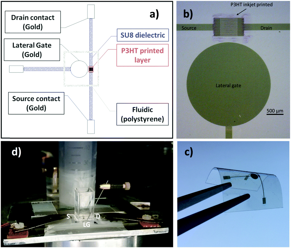 | ||
| Fig. 1 (a) Schematic representation and (b) optical microscope image of an EGOFET fabricated by ink-jet printing and standard photolithography – scale bar is 500 μm; (c) picture of the device fabricated on a poly(ethylene 2,6-naphthalate) (PEN) flexible substrate; (d) picture of the device after a polystyrene cell is glued around the transistor channel, the cell is connected to a water reservoir visible in the back. | ||
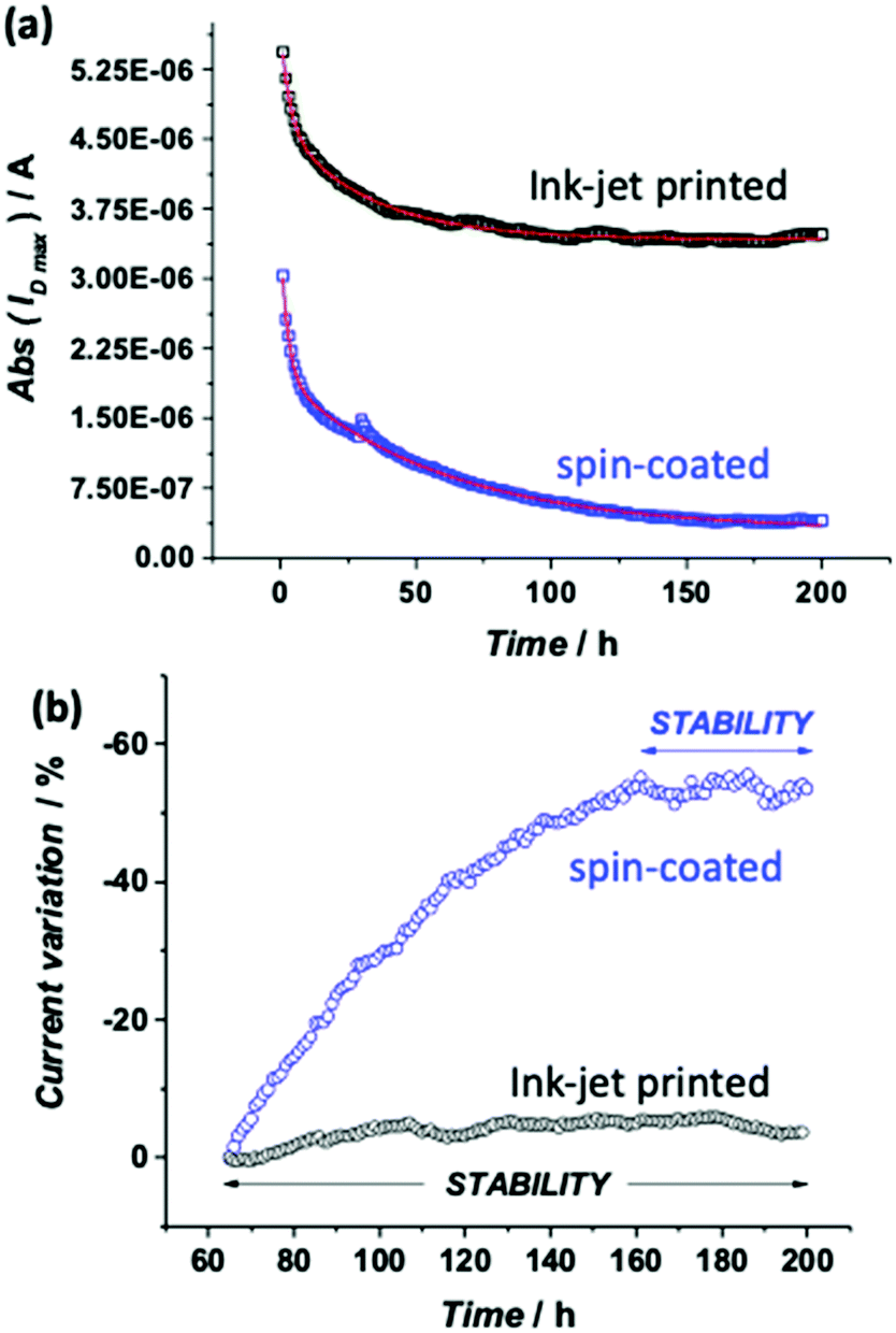 | ||
| Fig. 2 (a) Comparison between the time evolution of IDmax (source–drain current at the maximum transconductance) of EGOFETs comprising a spin-coated (blue squares) or an ink-jet printed (black squares) P3HT film; each data point is measured at an interval of 1 hour, so overall the experiments last more than 8 days. A bi-exponential fit (see text for details) of the experimental data is also provided as a solid red line. (b) Percentage variation of IDmax after the acquisition of the first 64 transfer curves till the 200th ones measured on an EGOFET comprising a spin-coated (blue circles) or an ink-jet printed (black circles) P3HT film. | ||
The fitting parameters for the two sets of analyzed data are listed in Table S2 (ESI†). The first row is relevant to the printed film, and the second to the spin-coated one. The IDmax of the printed EGOFET shows first a faster (τ1 = 3.22 ± 0.22 h) and pronounced decay followed by a much slower (τ2 = 32.03 ± 0.71 h) and less steep one up to reaching a steady state. The two decay components give almost the same contribution, since the ratio between their amplitudes A1/A2 is close to 1. Starting from the 64th cycle (ca. 2.5 days of operation), the relative variation of IDmax is lower than 5%, as can be seen in Fig. 2b. This is the magnitude of the relative random error observed in negative control experiments in a typical sensing experiment.17
As this is the highest error measured in the sensing experiment, stability of the EGOFET below this level can be considered acceptable. Hence, the stabilization process of the printed P3HT EGOFET can be considered completed typically after a couple of days of operation in water. If the device is kept in water from this point ahead, the current level can stay stable for up to a month, as can be seen from Fig. S5 (ESI†) where the average IDmax values measured 34 and 52 days after the stability characterization are reported. In a previous work it was demonstrated that a spin-coated P3HT reached stabilization even if just left to rest in water with no biasing as the most relevant process in the stabilization is the acquaintance of the film, processed from an organic solvent, with water.27 Some evidence has been gathered (data not shown) that this holds true also for the printed P3HT. An independent piece of spectroscopic evidence for the long-term stability of a printed P3HT in water will be provided later on in the text. From the point of view of future applications this is a very important aspect as, once the device is fabricated, it can be stored in water maybe in a packaging comprising a hydrogel layer in contact with the P3HT film. This should be enough to enable for a shelf life of a few weeks and a readily stable operation once the EGOFET is put into operation.
The comparison of the stabilization process of the printed P3HT film with that of the spin-coated one (Fig. 2a) shows that a much more pronounced decay and a slower kinetics are observed for the spin-coated device as shown also by the modelling parameters given in Table S2 (ESI†). Indeed, while the first exponential decay is comparable to that of the printed device, the second regime is much slower lasting almost twice the time. To gather deeper insights into such different kinetics of the stabilization process of printed and spin-coated P3HT films, a physical based modeling of the ID–VG transfer curves for two classes of devices was undertaken. To this end the measured ID–VG curves (symbols) along with the ID–VG characteristics predicted by the model (solid lines) are shown in Fig. 3. Specifically, in Fig. 3a and b the transfer characteristics at cycle numbers 1, 25, 50 and 200 are shown for the printed and spin coated P3HT respectively. A first comment concerns the overall drop of the source–drain current that for the printed film is −33% while it reaches a much lower value for the spin-coated film (−87%). Interestingly, an almost identical decay of the performance (−36% of IDmax) was observed for a second ink-jet printed EGOFET (Fig. S4, ESI†), confirming the good reproducibility of the processing technique and the consistency of the data.
 | ||
| Fig. 3 EGOFET transfer curves comprising an ink-jet printed (a) or a spin-coated (b) P3HT layer; cycles: 1, 25, 50 and 200. Symbols represent the measurements while solid lines represent the data calculated with the model. In the case of ink-jet printed devices, a duty cycle comprising a pulsing of VD with an on-time of 400 ms and an off-time of 30 ms was used, while the transfer curves of spin-coated EGOFETs were acquired according to the protocol described in ref. 27, where both VG and VD were pulsed. | ||
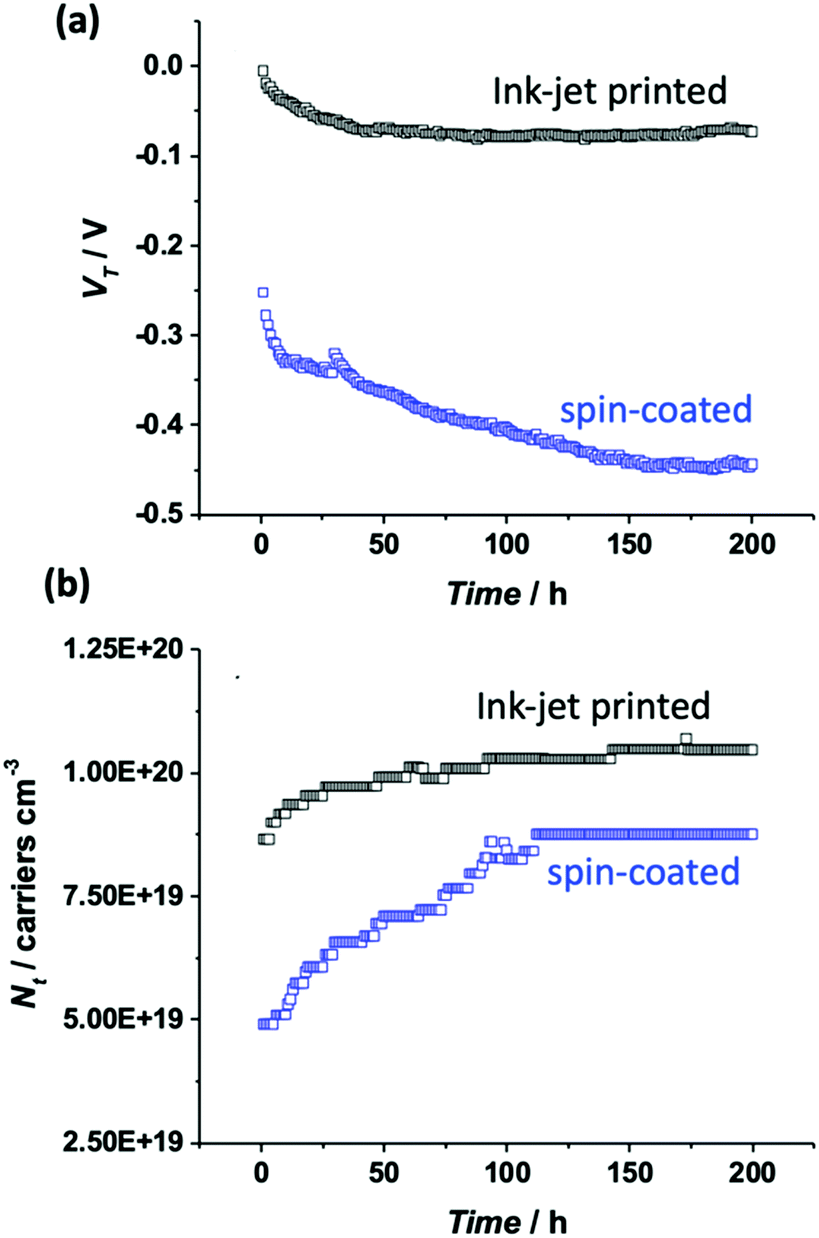
To accurately estimate parameters such as the transistor threshold voltage, VT, as well as the total density of localized (trap) states Nt from the elicited transfer characteristics, the electrical measurements were fitted with a physical-based numerical model. The model accounts for the charge transport in the P3HT semiconductor as well as the ion-modulated electrical-double-layer (EDL) accumulation at the electrolyte–semiconductor interface and at the gate–electrolyte interface. More in detail, the charge transport into the P3HT semiconductor accounts for both delocalized states and localized states. The hole concentration in the delocalized states is given by the Boltzmann statistic that reads hH = NHOMOexp[(EF − EHOMO)/(kBT)], where NHOMO is the total density of delocalized states in the Highest Occupied Molecular Orbital (HOMO), EF is the Fermi energy level, EHOMO is the HOMO energy level, kB is the Boltzmann constant and T is the temperature. The hole concentration in the localized states is calculated by solving the Fermi–Dirac integral accounting for an exponential distribution of localized states and reads ht = Ntexp[EF − EHOMO/(Et)], where Nt is the total density of localized states and Et is the energy disorder of the P3HT.
The drain–source current (eqn (2)) is calculated by numerically solving the drift-diffusion transport equation that reads
 | (2) |
 | (3) |
 | (4) |
C, for which Ep is close to 0.18 eV, we can directly obtain W from the ratio of the two lowest phonon sidebands. The absorption band of the weakly interacting H-aggregates can be approximated as | (5) |
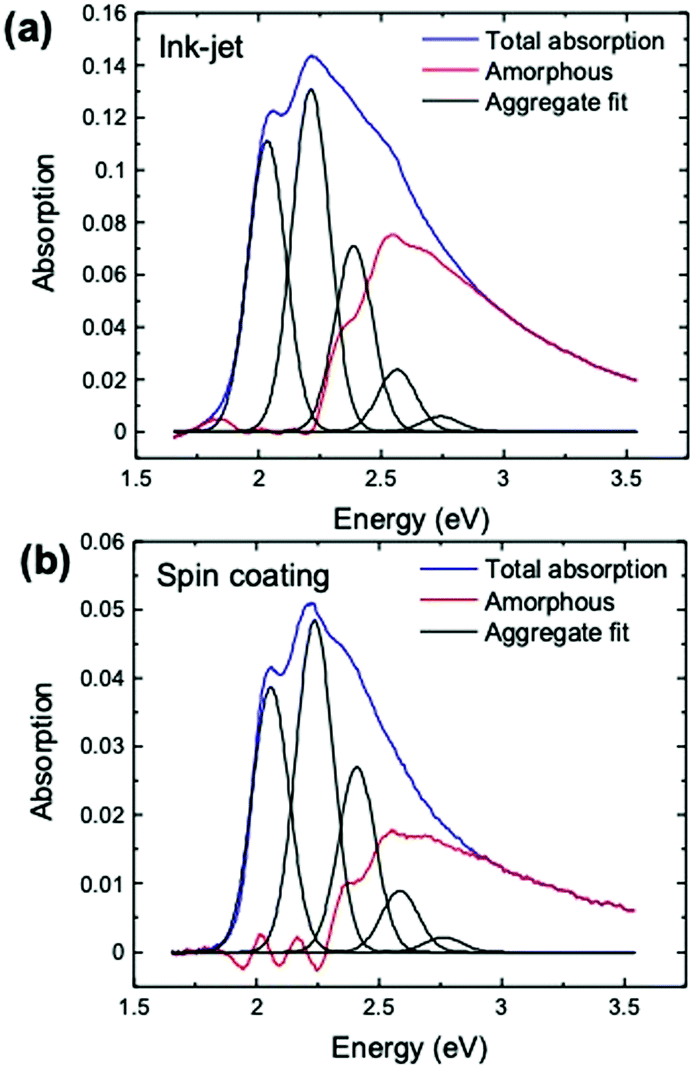
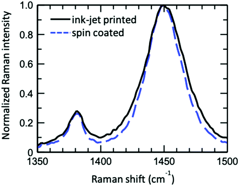
 over all vibrational states n. The vibrational progression is fitted using a Gaussian distribution with the full width at half maximum (FWHM), denoted as σ, being proportional to the inhomogeneous broadened absorption, and hence reflecting the disorder strength in the electronic coupling. Thus, the aggregate absorption can be numerically fitted, and the degree of aggregation is approximated by the ratio of the H-aggregate absorption to the total absorption. The absorption spectra for spin-coated and ink-jet printed P3HT films are given in Fig. 5a and b, respectively. By fitting the spectra, it is possible to extract the following parameters: E0-0, σ and W.4 The results of the fitting from ink-jet printed and spin-coated P3HT samples are summarized in Table 1. From the analysis of the absorption spectra results, ink-jet printed samples are slightly more disordered, as stated by the lower percentage of H-aggregates. However, lower W values are extracted for the spectra of these films, indicating that the aggregate regions, although smaller, could be of higher quality than those in the spin-coated films. In the latter, the percentage of amorphous regions is however comparatively lower. Interestingly, these results are in full agreement with the analysis carried out with the physical-based drain current model and also the Raman characterization of the two films corroborates the findings of UV-Vis spectra. Fig. 6 shows representative Ramans spectra of spin-coated and ink-jet printed P3HT films, excited under resonant conditions at 488 nm, in the region of C–C and CC phonon modes. Both spectra show similar features with a main band corresponding to the CC mode and a smaller peak due to the C–C phonon. The spectral analysis was carried out by fitting the double peak structure with Lorentzian curves. The results show that both samples share the same band peak positions: 1380.2 cm−1 for the C–C mode, while the CC mode is peaked at 1450.1 cm−1 and 1450.6 cm−1 for the spin-coated and ink-jet printed samples, respectively. These values are in excellent agreement with the reported Raman band peaks at 488 nm of a regio-regular P3HT.34 Particularly, the CC phonon energy is known to be strongly influenced by the degree of order in P3HT films and blueshifts substantially (∼20 cm−1) in the amorphous phase. Hence, the measured phonon band energies suggest a large degree of order in both samples. On the other hand, the full width at half maximum (FWHM) and the intensity ratios between the integrated intensities R = I(C–C)/I(CC) reveal subtle differences between the two samples. The FWHM values are 10.1 cm−1 (C–C) and 29.3 cm−1 (CC) for the spin-coated sample and 12.8 cm−1 (C–C) and 34.6 cm−1 (CC) for the ink-jet printed sample, respectively. While the CC linewidth is comparable to that reported in resonance for the regio-regular P3HT (∼32 cm−1),34 the ∼18% increase of the FWHM in the case of the ink-jet printed film suggests a partial disorder increase in this sample. Similar conclusions stem from the analysis of Raman spectra under the pre-resonant conditions at 633 nm. The whole set of measurements carried out on the two classes of films serving as channel materials in an EGOFET structure provides quite a consistent picture of the differences existing between the spin-coated and the ink-jet printed P3HT films. In Fig. 7, a pictorial representation of the P3HT structure for ink-jet printed (panel a) and spin-coated (panel b) films is provided.
 | ||
| Fig. 4 (a) Ink-jet printed and spin-coated P3HT based EGOFETs’ threshold voltage (a) VT, and (b) total density of localized (trap) states Nt as extracted from the modelling of the transfer characteristics (see text for details). | ||
 | ||
| Fig. 5 Comparison of the absorption spectra of ink-jet printed (a) and spin-coated (b) P3HT films. | ||
| E 0-0 (eV) | σ (meV) | W (meV) | Aggregate (%) | |
|---|---|---|---|---|
| Ink-jet | 2.025 ± 0.002 | 77 ± 1 | 45 ± 4 | 62 ± 1 |
| Spin-coating | 2.043 ± 0.004 | 74 ± 2 | 59 ± 8 | 71 ± 2 |
 | ||
| Fig. 6 Comparison of the resonant Raman spectra (C–C and CC modes) of ink-jet printed (solid black line) and spin-coated (blue dashed line) P3HT films, excited using a 488 nm laser. | ||
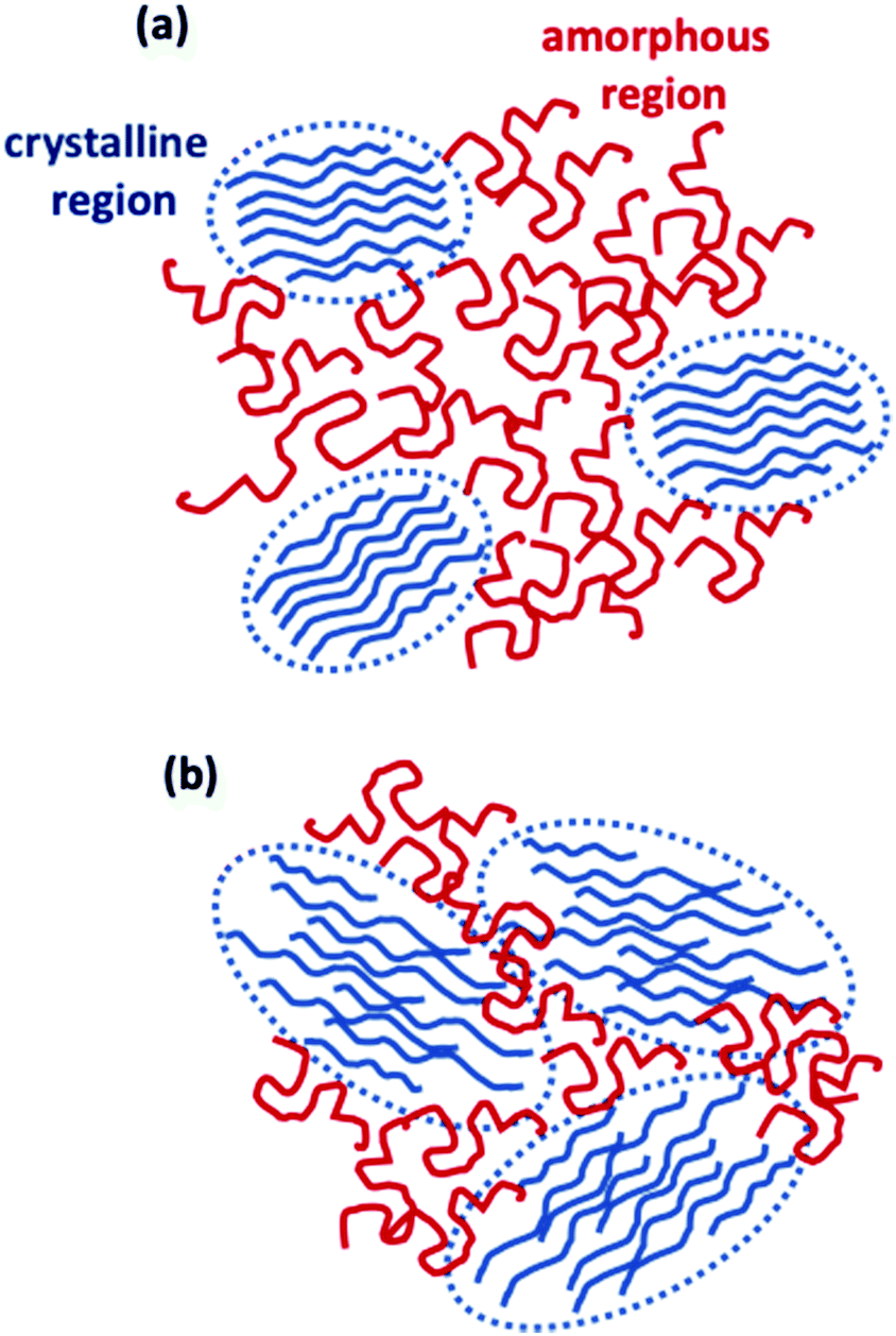 | ||
| Fig. 7 Pictorial representation of the P3HT structure for ink-jet printed (a) and spin-coated (b) films. In the printed film smaller crystalline regions with better π–π stacking can be found. The spin-coated one has larger and more crystalline regions with overall worse π–π stacking features. | ||
On the basis of the characterization and analyses, we can state that (i) the current stabilization process involving the printed P3HT film is much faster and the comparatively lower relative current decrease is mirrored by a lower relative increase in the number of trap states. Still, the overall number of trap states is higher than that extracted from the data measured on the spin-coated film. The UV-Vis characterization brings up a better quality of the crystalline regions that are however dispersed in a larger volume of amorphous film. The resonant Raman spectra show that the CC phonon linewidth is typical for a regio-regular P3HT and the slightly larger FWHM suggests a partial disorder increase in this sample. So, the printed films hold a lower energetic disorder but more abundant regions of amorphous material as shown in Fig. 7a; (ii) in contrast, the spin-coated film is characterized by a large drop of the current flowing in the channel region during the stabilization process that is mirrored by a large relative increase of the trap states before stabilization is reached. Overall the number of traps is however lower than that found in the printed film. This is corroborated by UV-Vis characterization that shows how the spin-coated film has a lower value for W, which is the exciton bandwidth, being inversely proportional to the crystalline quality of the H-aggregates. At the same time a higher relative occurrence of crystalline aggregate regions is present. This confirms that the film has comparatively less abundant amorphous regions but the crystalline regions present less energetic disorder (Fig. 7b).
The difference in the crystalline quality estimated for the ink-jet printed and spin-coated sample is likely ascribable to the different solvents employed during the semiconductor processing. Indeed, a higher boiling point solvent should lead to lower W.33 In particular, the impact of the solvent has been evaluated through UV-Vis spectroscopy as well, to provide essential pieces of information for the optimization of the parameters of ink-jet printed P3HT. Specifically, the absorption spectra of P3HT films with a concentration of 2.6 mg mL−1 spin-coated from chlorobenzene (CB, boiling point 132 °C) and ortho-dichlorobenzene (ODCB, boiling point 183 °C) have been compared. ODCB holds a higher viscosity and hence is more suitable in a printing process. Moreover, the P3HT films have been annealed for 15 minutes at 100 °C after spin-coating. The main results are summarized in Table 2. Those data clearly show that the higher boiling point solvent (ODCB) should be preferred to form as large aggregate domains as possible while annealing increases the order in the domains. Interestingly a decrease in W of about 20% has been found with ortho-dichlorobenzene with respect to the chlorobenzene samples (Table 2). These results are consistent with more specific works on the study of crystallinity by using X-ray diffraction and scattering. Also in these works an improvement of the electrical performance in the presence of well-packed crystalline P3HT domains has been reported.35–37
| Sample | E 0-0 (eV) | σ (meV) | W (meV) | A max | Aggregate [%] |
|---|---|---|---|---|---|
| o-Dichlorobenzene (ODCB) | 2.04 | 73 | 111 | 0.05 | 66 |
| Chlorobenzene (CB) | 2.03 | 73 | 133 | 0.08 | 65 |
Last but not least, we have also investigated how to improve the shelf-life of ink-jet printed devices. The possibility to store devices for a long time is crucial to look forward to commercial exploitations. To this end, the possibility to store devices in air or water was investigated utilizing UV-Vis spectroscopy, and the data are given in Fig. 8a and b, respectively. These conditions were chosen as they can be easily implemented in an industrial process. According to the measurements shown in Fig. 8a, storage in air results in intense bleaching of the printed P3HT semiconductor with the total absorption intensity decreasing by around 40% and hence a critical degradation of the degree of order of the film occurs. On the other hand, storage in water prevents P3HT film degradation, as water can protect the film from oxidation. In this case, only slight changes in the intensity of the spectrum can be seen, probably due to limited rearrangement at the semiconductor/water interface. This is in agreement with a study showing that stabilization kinetics very similar to the one shown in Fig. 2a can be measured for a spin-coated or a printed P3HT film that is kept in water for several days and is measured once a day.27 The stability of P3HT kept in water opens the opportunity to process and store EGOFETs for industrial development purposes.
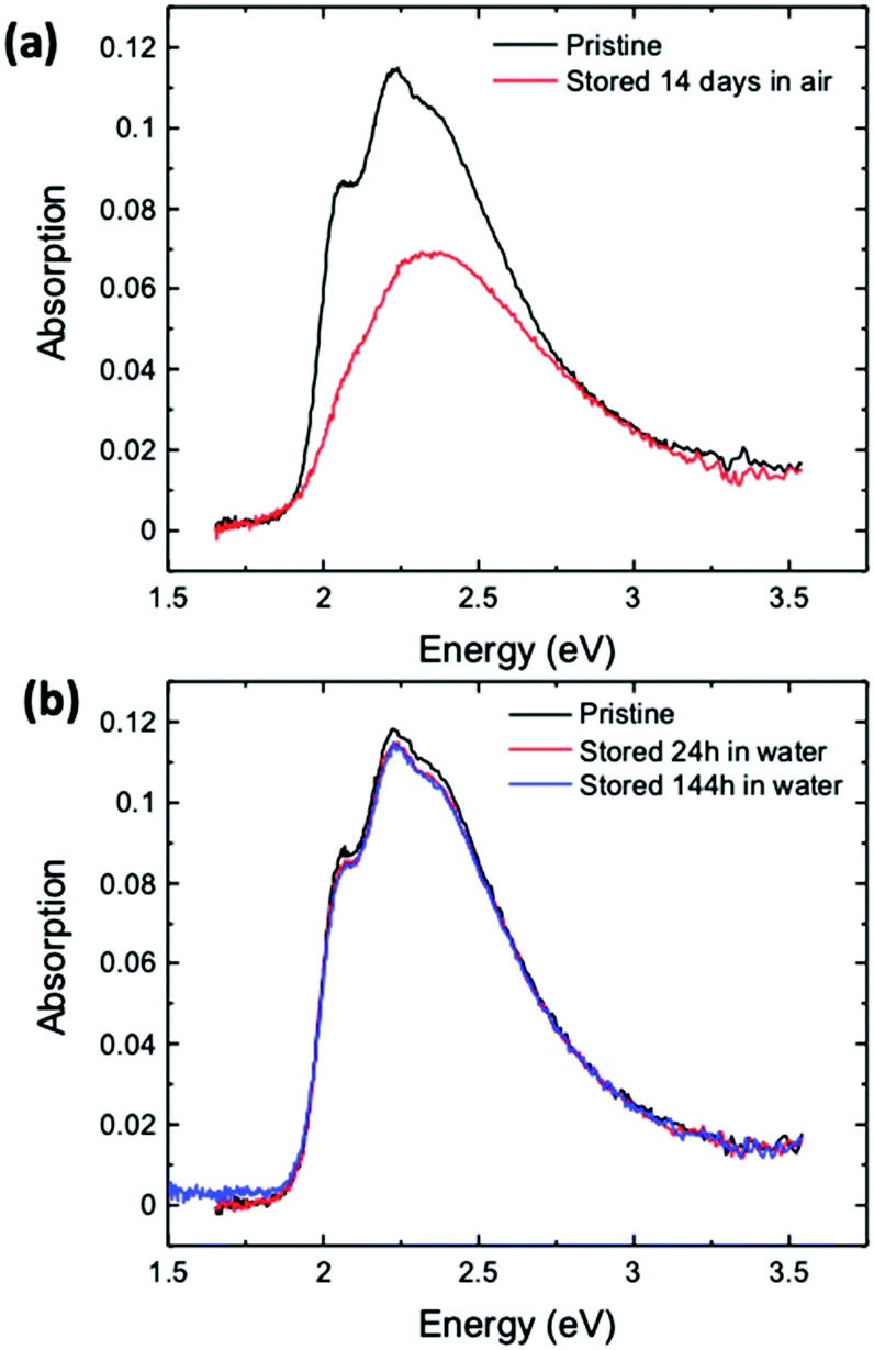 | ||
| Fig. 8 Evolution of absorption spectra for P3HT films stored in air (a) or immersed in water (b). | ||
Conclusions
A systematic comparison is proposed between a spin-coated and an ink-jet printed regio-regular polycrystalline P3HT serving as the channel material in an electrolyte-gated field effect transistor device. While P3HT is a widely studied and characterized material, extensively employed as semiconductor in a number of different devices, a systematic comparison of the structure–performance features of printed and spin-coated ones has been very seldom proposed.Here a study of a cost-effective large area compatible printed P3HT in an EGOFET configuration has been carried out combining electrical, optical and Raman characterization. All the gathered evidence concurs to prove that this polycrystalline printed film holds higher quality crystals in terms of π–π stacking but a larger fraction of amorphous regions. The lower energetic disorder, ascribed to the use of a higher boiling point and more viscous solvent, enables also for a faster stabilization of the output current when the device is exposed to and/or operated in water. The stability of the cost-effective printed P3HT EGOFET is tested continuously for eight days, proving that a very stable operation regime can be reached in approximately two days, which is much faster than that achieved with a spin-coated film. Last but not least, it has been shown that the stabilization process of the printed P3HT film can be achieved by just storing the device in water for two days. An explanation for this occurrence is provided considering that the acquaintance of the pristine P3HT film with the water environment, even in the absence of a bias, is the main driving force towards stabilization. From the point of view of future applications this is a very important aspect as, once the device is fabricated, it can be stored in water maybe in a packaging comprising a hydrogel layer in contact with the P3HT film. This should be enough to enable for a shelf life of a few weeks and a readily stable operation once the EGOFET is put into operation. The EGOFET device structure has been also optimized by designing a large lateral coplanar gate that contributes to confer mechanical and electrical stability.
These features all concur to make printed P3HT based EGOFETs ideal candidates for bioelectronic sensing applications.
Conflicts of interest
There are no conflicts to declare.Acknowledgements
This work was partially carried out at PoliFab, the micro and nano-technology center of the Politecnico di Milano. PON SISTEMA (MIUR), H2020 - Electronic Smart Systems – SiMBiT: Single molecule bio-electronic smart system array for clinical testing (Grant agreement ID: 824946), Future in Research APQ Ricerca Regione Puglia “Programma regionale a sostegno della specializzazione intelligente e della sostenibilità sociale ed ambientale – FutureInResearch” – “BEND” Biosensori elettronici intelligenti per la diagnosi precoce di malattie neurodegenerative (B164PG8), “PMGB -Sviluppo di piattaforme meccatroniche, genomiche e bioinformatiche per l'oncologia di precisione” – ARS01_01195 – PON “RICERCA E INNOVAZIONE” 2014–2020 projects, the European Union, Italian Government and Lombardia Region for the project BIOSCREEN (POR FESR 2014–2020, ID number 1831459, CUP E81B20000320007), and CSGI are acknowledged for partial financial support.Notes and references
- M. Parmeggiani, A. Verna, A. Ballesio, M. Cocuzza, E. Piatti, V. Fra, C. F. Pirri and S. L. Marasso, Sensors, 2019, 19, 1–12 CrossRef.
- M. Mas-Torrent, D. Den Boer, M. Durkut, P. Hadley and A. P. H. J. Schenning, Nanotechnology, 2004, 15, 265–269 CrossRef.
- J. Ficker, A. Ullmann, W. Fix, H. Rost and W. Clemens, J. Appl. Phys., 2003, 94, 2638–2641 CrossRef CAS.
- S. Brixi, O. A. Melville, N. T. Boileau and B. H. Lessard, J. Mater. Chem. C, 2018, 6, 11972–11979 RSC.
- L. Motiei, Y. Yao, J. Choudhury, H. Yan, T. J. Marks, M. E. van der Boom and A. Facchetti, J. Am. Chem. Soc., 2010, 132, 12528–12530 CrossRef CAS.
- E. Macchia, D. Alberga, K. Manoli, G. F. Mangiatordi, M. Magliulo, G. Palazzo, F. Giordano, G. Lattanzi and L. Torsi, Sci. Rep., 2016, 6, 28085 CrossRef CAS.
- S. K. Park, Y. H. Kim, J. I. Han, D. G. Moon, W. K. Kim and M. G. Kwak, Synth. Met., 2003, 139, 377–384 CrossRef CAS.
- I. McCulloch, M. Heeney, C. Bailey, K. Genevicius, I. MacDonald, M. Shkunov, D. Sparrowe, S. Tierney, R. Wagner, W. Zhang, M. L. Chabinyc, R. J. Kline, M. D. McGehee and M. F. Toney, Nat. Mater., 2006, 5, 328–333 CrossRef CAS.
- T. Yamamoto, D. Komarudin, M. Arai, B.-L. Lee, H. Suganuma, N. Asakawa, Y. Inoue, K. Kubota, S. Sasaki, T. Fukuda and H. Matsuda, J. Am. Chem. Soc., 1998, 120, 2047–2058 CrossRef CAS.
- H. Sirringhaus, P. J. Brown, R. H. Friend, M. M. Nielsen, K. Bechgaard, B. M. W. Langeveld-Voss, A. J. H. Spiering, R. A. J. Janssen, E. W. Meijer, P. Herwig and D. M. de Leeuw, Nature, 1999, 401, 685–688 CrossRef CAS.
- S. Bellani, D. Fazzi, P. Bruno, E. Giussani, E. V. Canesi, G. Lanzani and M. R. Antognazza, J. Phys. Chem. C, 2014, 118, 6291–6299 CrossRef CAS.
- K. Rahimi, I. Botiz, J. O. Agumba, S. Motamen, N. Stingelin and G. Reiter, RSC Adv., 2014, 4, 11121–11123 RSC.
- P. Ehrenreich, S. T. Birkhold, E. Zimmermann, H. Hu, K. D. Kim, J. Weickert, T. Pfadler and L. Schmidt-Mende, Sci. Rep., 2016, 6, 1–8 CrossRef.
- G. Jo, J. Jung and M. Chang, Polymers, 2019, 11, 332 CrossRef.
- S. H. Kim, K. Hong, W. Xie, K. H. Lee, S. Zhang, T. P. Lodge and C. D. Frisbie, Adv. Mater., 2013, 25, 1822–1846 CrossRef CAS.
- E. Macchia, R. A. Picca, K. Manoli, C. Di Franco, D. Blasi, L. Sarcina, N. Ditaranto, N. Cioffi, R. Österbacka, G. Scamarcio, F. Torricelli and L. Torsi, Mater. Horiz., 2020, 7, 999–1013 RSC.
- E. Macchia, K. Manoli, B. Holzer, C. Di Franco, M. Ghittorelli, F. Torricelli, D. Alberga, G. F. Mangiatordi, G. Palazzo, G. Scamarcio and L. Torsi, Nat. Commun., 2018, 9, 3223 CrossRef.
- R. A. Picca, K. Manoli, E. Macchia, L. Sarcina, C. Di Franco, N. Cioffi, D. Blasi, R. Österbacka, F. Torricelli, G. Scamarcio and L. Torsi, Adv. Funct. Mater., 2020, 30, 1904513 CrossRef CAS.
- E. Macchia, K. Manoli, C. Di Franco, G. Scamarcio and L. Torsi, Anal. Bioanal. Chem., 2020, 412, 5005–5014 CrossRef CAS.
- R. A. Picca, D. Blasi, E. Macchia, K. Manoli, C. Di Franco, G. Scamarcio, F. Torricelli, A. Zurutuza, I. Napal, A. Centeno and L. Torsi, in 2019 IEEE 8th International Workshop on Advances in Sensors and Interfaces (IWASI), 2019, pp. 136–138.
- E. Macchia, A. Tiwari, K. Manoli, B. Holzer, N. Ditaranto, R. A. Picca, N. Cioffi, C. Di Franco, G. Scamarcio, G. Palazzo and L. Torsi, Chem. Mater., 2019, 31, 6476–6483 CrossRef CAS.
- E. Macchia, K. Manoli, B. Holzer, C. Di Franco, R. A. Picca, N. Cioffi, G. Scamarcio, G. Palazzo and L. Torsi, Anal. Bioanal. Chem., 2019, 411, 4899–4908 CrossRef CAS.
- D. Blasi, L. Sarcina, A. Tricase, A. Stefanachi, F. Leonetti, D. Alberga, G. F. Mangiatordi, K. Manoli, G. Scamarcio, R. A. Picca and L. Torsi, ACS Omega, 2020, 5, 16762–16771 CrossRef CAS.
- S. K. Sailapu, E. Macchia, I. Merino-Jimenez, J. P. Esquivel, L. Sarcina, G. Scamarcio, S. D. Minteer, L. Torsi and N. Sabaté, Biosens. Bioelectron., 2020, 156, 112103 CrossRef CAS.
- E. Macchia, L. Sarcina, R. A. Picca, K. Manoli, C. Di Franco, G. Scamarcio and L. Torsi, Anal. Bioanal. Chem., 2020, 412, 811–818 CrossRef CAS.
- E. Macchia, K. Manoli, C. Di Franco, R. A. Picca, R. Österbacka, G. Palazzo, F. Torricelli, G. Scamarcio and L. Torsi, ACS Sens., 2020, 5, 1822–1830 CrossRef CAS.
- R. A. Picca, K. Manoli, E. Macchia, A. Tricase, C. Di Franco, G. Scamarcio, N. Cioffi and L. Torsi, Front. Chem., 2019, 7, 667 CrossRef CAS.
- D. P. McMahon, D. L. Cheung, L. Goris, J. Dacuña, A. Salleo and A. Troisi, J. Phys. Chem. C, 2011, 115, 19386–19393 CrossRef CAS.
- C. Wang, L. H. Jimison, L. Goris, I. McCulloch, M. Heeney, A. Ziegler and A. Salleo, Adv. Mater., 2010, 22, 697–701 CrossRef CAS.
- J. Rivnay, R. Noriega, J. E. Northrup, R. J. Kline, M. F. Toney and A. Salleo, Phys. Rev. B: Condens. Matter Mater. Phys., 2011, 83, 121306 CrossRef.
- J. Clark, J.-F. Chang, F. C. Spano, R. H. Friend and C. Silva, Appl. Phys. Lett., 2009, 94, 163306 CrossRef.
- R. Giridharagopal, L. Q. Flagg, J. S. Harrison, M. E. Ziffer, J. Onorato, C. K. Luscombe and D. S. Ginger, Nat. Mater., 2017, 16, 737–742 CrossRef CAS.
- H. Sinno, S. Fabiano, X. Crispin, M. Berggren and I. Engquist, Appl. Phys. Lett., 2013, 102, 113306 CrossRef.
- W. C. Tsoi, D. T. James, J. S. Kim, P. G. Nicholson, C. E. Murphy, D. D. C. Bradley, J. Nelson and J.-S. Kim, J. Am. Chem. Soc., 2011, 133, 9834–9843 CrossRef CAS.
- M. Xiao, X. Zhang, Z. J. Bryan, J. Jasensky, A. J. McNeil and Z. Chen, Langmuir, 2015, 31, 5050–5056 CrossRef CAS.
- J. K. Keum, K. Xiao, I. N. Ivanov, K. Hong, J. F. Browning, G. S. Smith, M. Shao, K. C. Littrell, A. J. Rondinone, E. Andrew Payzant, J. Chen and D. K. Hensley, CrystEngComm, 2013, 15, 1114–1124 RSC.
- Z. Yu, H. Yan, K. Lu, Y. Zhang and Z. Wei, RSC Adv., 2012, 2, 338–343 RSC.
Footnote |
| † Electronic supplementary information (ESI) available. See DOI: 10.1039/d0tc03342a |
| This journal is © The Royal Society of Chemistry 2020 |