DOI:
10.1039/C5RA00091B
(Paper)
RSC Adv., 2015,
5, 18159-18166
Noble-metal-free Cu2S-modified photocatalysts for enhanced photocatalytic hydrogen production by forming nanoscale p–n junction structure†
Received
3rd January 2015
, Accepted 4th February 2015
First published on 4th February 2015
Abstract
Developing efficient noble-metal-free photocatalysts is of great importance for the large-scale application of photocatalytic hydrogen production. Herein, low-cost and environment-friendly p-type Cu2S was successfully loaded on n-type CdS photocatalyst by an in situ method to achieve efficient Cu2S/CdS hybrid photocatalysts. Cu2S nanoparticles of ca. 50 nm were intimately assembled on the surface of polyhedral CdS nanocrystals, giving rise to the formation of numerous nanoscale p–n junctions between p-type Cu2S and n-type CdS. Compared to single CdS, Cu2S/CdS exhibited increased photocatalytic hydrogen production under visible light irradiation. The generated nanoscale p–n junctions in Cu2S/CdS, leading to the enhanced charge separation efficiency and better utilization of visible light, were crucial to the improved photocatalytic activity. During the photocatalytic reaction, Cu2S nanoparticles captured the photogenerated holes in CdS and served as the active sites for the surface oxidation reaction. The photocatalytic property of Cu2S/CdS photocatalysts was influenced by the Cu/Cd molar ratio, with the optimal one of 0.05. P-type Cu2S could also be utilized for improving the photocatalytic activities of n-type ZnIn2S4 and n-type TiO2 by forming efficient p–n junctions, indicating the general applicability of p-type Cu2S. This work demonstrates that forming p–n junction structure was a useful strategy for developing efficient noble-metal-free hybrid photocatalysts.
1. Introduction
Photocatalytic hydrogen production from water using solar energy has been considered as a promising route to solve the increasing energy and environmental problems.1–3 The key issue for its industrial application is to develop photocatalysts necessitating high efficiency, long-term stability, and low cost. However, most of semiconductor photocatalysts owns poor activity due to rapid charge recombination and insufficient surface reactive sites. Cocatalysts, which can effectively capture the photogenerated electrons/holes to enhance the charge separation efficiency, provide active sites for surface redox reaction, and decrease the surface reaction overpotential, are believed to be essential to achieving highly efficient photocatalytic hydrogen production.4
The most common and effective cocatalyst is Pt, which is widely applied for various photocatalysts. Other noble metals, such as Ru, Rh, Au and Pd, are also effective cocatalysts owing to the similar physicochemical properties like Pt.5,6 Nonetheless, the high price and low reserve of noble metals limit the large-scale application. Therefore, seeking efficient noble-metal-free photocatalysts is of critical importance. Recently, it has been demonstrated that a series of transition metal sulfides could promote the photocatalytic hydrogen production instead of Pt. Li's group reported that loading MoS2 or WS2 on CdS photocatalysts could give rise to efficient charge separation by forming intimate heterojunctions to achieve high activities.7,8 Xu's group revealed that NiS could act as efficient cocatalyst to significantly improve the hydrogen production of CdS photocatalysts. The apparent quantum efficiency of NiS/CdS at 420 nm reached 51.3%.9 Xie's group discovered that CuS could accelerate the photogenerated charge separation of CdS photocatalysts and subsequently the photocatalytic hydrogen production.10 Besides of CdS, the photocatalytic properties of various semiconductor photocatalysts such as CdxZn1−xS, CuGa3S5, TiO2, ZnO and C3N4 could also be enhanced by the deposition of such metal sulfides, indicating their general applicability.11–15 However, up to now, highly efficient transition-metal sulfide promoters with low price and earth-abundant elements are still limited. Meanwhile, the reported action mechanisms of such metal sulfides are quite different. As a consequence, it is necessary to study the general coupling principle between photocatalysts and such transition-metal sulfides and as a guidance to develop efficient noble-metal-free hybrid photocatalysts.
The basic requirement of coupling different semiconductors to enhance the photocatalytic activity is to form efficient heterojunction structure between different components, which is crucial to the improvement of charge separation efficiency. For example, as noble metal is deposited on semiconductor photocatalysts, the Schottky junction is generated between the noble metal and the semiconductor photocatalyst, which can lead to the efficient charge separation.4 Coupling semiconductors with different band structures to generate heterojunction structure can also result in the efficient charge separation.16 When p-type semiconductor is combined with n-type semiconductor, p–n junction can be formed between the two semiconductors. Across the p–n junction region, a built-in electric field is achieved, which can efficiently promote the separation of photogenerated electrons/holes.17 As we know, a number of reported photocatalysts are n-type semiconductors, such as CdS, ZnIn2S4 and TiO2.18–20 Therefore, Coupling suitable p-type semiconductors to promote the photocatalytic properties of n-type semiconductor photocatalysts can be expected. P-type NiO and p-type NiS have been demonstrated to be efficient cocatalysts to promote the photocatalytic activities of n-type semiconductor photocatalysts by forming p–n junctions.21,22 However, more efficient p-type semiconductor promoters, especially the ones with wide applicability should be explored.
Cu2S is a p-type semiconductor with a bulk bandgap of 1.2 eV.23 Due to its low cost and earth-abundant elements, Cu2S has been utilized for solar cells, optoelectronic devices and photocatalytic degradation of organic pollutants.24–28 However, the utilization of Cu2S in the area of photocatalytic hydrogen production has been seldom reported.29 Herein, we firstly prepared n-type CdS nanocrystals with polyhedral morphology. Then Cu2S nanoparticles were deposited by an in situ method to obtain Cu2S/CdS photocatalysts. A number of well-dispersed nanoscale p–n junctions were developed in the hybrid photocatalysts, which could efficiently improve the charge separation, leading to the much enhanced photocatalytic activity. P-type Cu2S was also coupled with n-type TiO2 and n-type ZnIn2S4. Interestingly, the improved activities were also achieved by forming nanoscale p–n junction structure, indicating the good applicability of p-type Cu2S.
2. Experimental
Cadmium nitrate tetrahydrate (Cd(NO3)2·4H2O), copper nitrate trihydrate (Cu(NO3)2·3H2O), sodium hydroxide (NaOH), sodium sulfide nonahydrate (Na2S·9H2O), sodium sulfite (Na2SO3), thioacetamide (C2H5NS), and ethanol (C2H6O) were purchased from Sinopharm Chemical Reagent Co., Ltd. All chemicals were used as purchased without further purification.
2.1 Synthesis of CdS photocatalysts
CdS photocatalysts were synthesized by a hydrothermal method. Briefly, 0.01 mol of Cd(NO3)2·4H2O was firstly added into 50 mL of 1.0 M NaOH aqueous solution. The suspension was stirred uniformly and 0.02 mol of thioacetamide was subsequently added with magnetic stirring. The obtained suspension was then heated for 48 h at 200 °C in a Teflon-lined autoclave. After the autoclave cooled naturally in air, the products were washed with ethanol and deionized water several times and dried in vacuum at 80 °C for 5 h.
2.2 Deposition of CuxS onto CdS photocatalysts
CuxS was deposited onto CdS photocatalysts by an in situ method. Before photocatalytic hydrogen production, appropriate amounts of Cu(NO3)2 solution were added into the Na2SO3/Na2S reaction solution containing 0.2 g of CdS powders. The suspension was then stirred for 0.5 h with nitrogen purged to obtain CuxS/CdS hybrid photocatalysts for photocatalytic reaction. The achieved products were denoted as CuxS/CdS-n, where n represented the Cu/Cd molar ratio. Pure CuxS was also synthesized for analysis. Typically, 0.005 mol of Cu(NO3)2·3H2O was added into 190 mL of 0.25 M Na2SO3/0.35 M Na2S aqueous solution, and stirred for 0.5 h with nitrogen purged. The obtained products were collected, washed with deionized water, and dried in vacuum at 80 °C for 5 h.
2.3 Characterization
The X-ray powder diffraction (XRD) pattern was examined by a PANalytical X'pert MPD Pro X-ray diffractometer (Cu Kα radiation). UV-visible (UV-vis) absorption spectrum was recorded using a HITACHI U-4100 spectrophotometer. The morphology of the photocatalysts was characterized with a JEOL JSM-7800F field-emission scanning electron microscope (FESEM), to which an Oxford energy dispersive X-ray spectroscopy (EDX) system X-max50 was coupled for EDX-SEM mapping analysis. The close examination of the morphology was carried out on a JEOL 1200CX transmission electron microscope (TEM). The X-ray photoelectron spectroscopy (XPS) measurement was conducted on a Axis Ultra, Kratos (UK) multifunctional X-ray photoelectron spectrometer (Al Kα radiation). Binding energies were calibrated relative to the C 1s peak (284.8 eV) from adventitious carbon adsorbed on the surface of the samples. The photoluminescence (PL) property was analyzed at room temperature on a PTI QM-4 fluorescence spectrophotometer.
2.4 Photocatalytic hydrogen production
Photocatalytic hydrogen production was tested with stirring under visible light irradiation in a side irradiation Pyrex cell with a water jacket (Fig. S1†). The efficient irradiation area of the cell was 15.90 cm2. 0.2 g of photocatalysts were added into 190 mL of aqueous solution containing 0.25 M Na2SO3/0.35 M Na2S as sacrificial reagents, and appropriate amount of CuxS was deposited by the above mentioned in situ method. Nitrogen was purged through the cell before reaction to remove oxygen. A 300 W Xe lamp equipped with a cutoff filter (λ ≥ 420 nm) was used as the light source, and the temperature was kept at 35 ± 0.2 °C for all photocatalytic reactions by flowing water with controlled temperature of 35 °C through the water jacket. The amount of generated hydrogen was detected by an on-line TCD gas chromatograph (NaX zeolite column, N2 as carrier gas). The blank experiments in the absence of irradiation or photocatalyst showed no appreciable hydrogen production. The apparent quantum yield (AQY) was calculated by the eqn (1). Specifically, in order to test the AQY of the photocatalyst at 420 nm, a 420 nm band-pass filter was coupled with the 300 W Xe lamp as the light source. The amount of generated hydrogen was detected by an on-line TCD gas chromatograph, and the light intensity at 420 nm was measured by a fiber optic spectrometer. The calculation method of the number of incident photons can be found in the ESI.†| |
 | (1) |
3. Results and discussion
3.1 Demonstration of generating Cu2S and Cu2S/CdS
Fig. 1 shows the XRD patterns of different samples. The diffraction peaks of hydrothermally synthesized CdS could be well assigned to wurtzite CdS with a typical hexagonal structure (JCPDS no. 06-0314).30 The sharp peaks indicated their good crystallinity. Subsequently, the diffraction peaks of as-synthesized CuxS observed at 2θ values of 27.91°, 32.38°, 46.46°, and 54.88° could be indexed to (111), (200), (220) and (311) planes of Cu2S cubic phase (JCPDS no. 84-1770).31,32 For CuxS/CdS hybrid photocatalysts, there were only diffraction peaks corresponding to those of wurtzite CdS, possibly owing to the low loading amount and high dispersion of CuxS particles. It was noticed that the intensities of CdS diffraction peaks were decreased with the increasing amount of CuxS, probably due to the covering of CuxS particles onto the surface of CdS.
 |
| | Fig. 1 XRD patterns of CdS, CuxS, and CuxS/CdS samples with various Cu/Cd molar ratios. | |
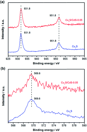
To further analyse the valance states of copper in CuxS and CuxS/CdS, XPS measurements were carried out. As indicated in Fig. 2a, the Cu 2p XPS spectrum of CuxS revealed that the binding energies of Cu 2p3/2 and Cu 2p1/2 peaks were respectively located at 931.8 and 951.8 eV, which corresponded to the typical values for Cu+ in Cu2S.33,34 Meanwhile, there were no “shake-up” peaks in the higher binding energy direction, indicating the absence of CuS. In addition, the generation of Cu2S could be demonstrated by the associated Auger line (Cu LMM) at 569.6 eV in Fig. 2b, which was the typical value of Cu2S.33 It was noted in Fig. 2 that the observed Cu 2p XPS and Auger Cu LMM peaks of CuxS/CdS were at the same positions with those for single CuxS, which revealed that copper in CuxS/CdS was also in the form of Cu+. On the basis of XRD and XPS results, we can summarize that Cu2S and Cu2S/CdS photocatalyst were finally synthesized in the present study.
 |
| | Fig. 2 (a) Cu 2p XPS spectra and (b) the Auger Cu LMM spectra of CuxS and CuxS/CdS-0.05 samples. | |
As presented in the experimental section, Cu2S was obtained by adding 0.005 mol of Cu(NO3)2·3H2O into 190 mL of 0.25 M Na2SO3/0.35 M Na2S solution. In order to clarify the reaction process, 0.005 mol of Cu(NO3)2·3H2O was respectively added into 190 mL of 0.25 M Na2SO3 or 0.35 M Na2S solution for comparison. When Cu2+ was added into Na2SO3 solution and stirred for 0.5 h, the solution was still transparent and no solid products could be obtained. In the case of Cu2+ into Na2S solution, black powders could be achieved, which could be denoted as CuxS (Na2S). The XRD pattern of CuxS (Na2S) showed the typical diffraction peaks assigned to both Cu2S and CuS (Fig. S2†). It is inferred that as Cu2+ was added into the solution with Na2S, the eqn (2) would occur to form CuS due to its low solubility product (Ksp) of 6.3 × 10−36.35 Since the amount of S2− (0.0665 mol) in the solution was much higher than the amount of added Cu2+ (0.005 mol), parts of CuS could be reduced to Cu2S by excess S2− according to the eqn (3). Therefore, both Cu2S and CuS were generated by adding Cu2+ into Na2S solution. However, when Na2SO3 was present in the reaction solution, SO32− would react with S22− by the eqn (4), accelerating the formation of Cu2S by the eqn (3). Meanwhile, CuS could be reduced to Cu2S by SO32− according to the eqn (5). As a consequence, only Cu2S was achieved by adding Cu2+ into the solution with both Na2SO3 and Na2S.
| | |
2CuS + S2− → Cu2S + S22−
| (3) |
| | |
S22− + SO32− → S2O32− + S2−
| (4) |
| | |
2CuS + SO32− + 2OH− → Cu2S + SO42− + S2− + H2O
| (5) |
3.2 Morphology and structure of Cu2S/CdS hybrid photocatalysts
The morphology of Cu2S/CdS hybrid photocatalysts was examined by FESEM. As shown in Fig. 3a and b, CdS nanocrystals exhibited polyhedral structure that had a size of several hundred nanometers. The surface of CdS polyhedrons is very clean and smooth. When Cu2S was deposited to form Cu2S/CdS, it was observed in Fig. 3c and d that a number of Cu2S nanoparticles with a diameter of ca. 50 nm were adhered to the surface of CdS polyhedrons, and the heterojunctions between Cu2S and CdS were acquired for Cu2S/CdS-0.05. As the loading amount of Cu2S was improved, more small nanoparticles deposited on CdS polyhedrons could be found for Cu2S/CdS-0.1 in Fig. 3e and f. Particularly, the surfaces of CdS polyhedrons were nearly covered by the Cu2S nanoparticles, and the polyhedral structure of CdS was hardly detected (Fig. 3e). Meanwhile, plenty of Cu2S nanoparticles became to aggregate together (Fig. 3f).
 |
| | Fig. 3 FESEM images of (a and b) CdS; (c and d) Cu2S/CdS-0.05; and (e and f) Cu2S/CdS-0.1. | |
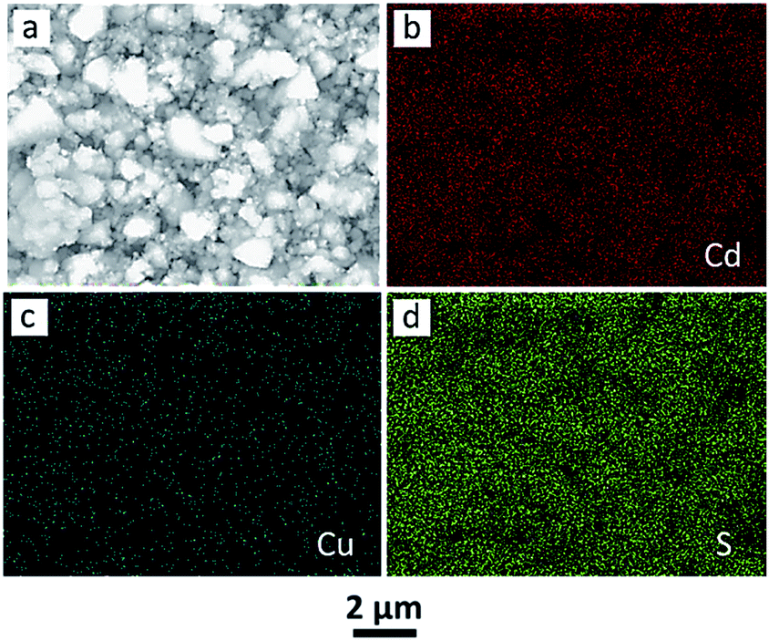
In order to further confirm the successful deposition of Cu2S nanoparticles, EDX-SEM elemental mapping analysis of Cu2S/CdS-0.05 was carried out. As displayed in Fig. 4, such mapping results demonstrated the presence of cadmium, copper and sulfur. In addition, it was observed in Fig. 4c that copper was uniformly dispersed, which indicated that well-dispersed heterojunctions between CdS and Cu2S could be generated. The deposition process of Cu2S nanoparticles could be illustrated in Fig. S3.† CdS polyhedrons, serving as the substrates to deposit Cu2S nanoparticles, were firstly dispersed into Na2SO3/Na2S aqueous solution. Appropriate amount of aqueous solution containing Cu2+ ions was then dripped into the above suspension. Cu2S would subsequently nucleate on the surface of polyhedral CdS nanocrystals and grew into crystallized nanoparticles. The Cu/Cd molar ratios of different Cu2S/CdS photocatalysts were also determined by EDX system coupled with FESEM. As shown in Table S1,† with the increase of added Cu precursor, the Cu/Cd molar ratio by EDX gradually increased. Meanwhile, the measured Cu/Cd molar ratios are a little higher than the added ratios in the synthesis of Cu2S/CdS samples, possibly due to Cu2S nanoparticles deposited on the surface of polyhedral CdS nanocrystals (the analysis diameter and depth for the used EDX system is ca. 1.0 μm).
 |
| | Fig. 4 (a) FESEM image of Cu2S/CdS-0.05 and (b–d) the corresponding EDX-SEM mapping images of Cd, Cu and S in Cu2S/CdS-0.05. The scale bar is 2 μm in each image. | |
TEM and HRTEM measurements were performed to identify the detailed structure of Cu2S/CdS-0.05 hybrid photocatalysts. Fig. 5a shows a typical CdS polyhedron deposited by the highly dispersed Cu2S nanoparticles with a diameter of ca. 50 nm (marked by red circles), which led to the formation of nanoscale heterojunctions between the CdS nanocrystal and Cu2S nanoparticles. A close examination in Fig. 5b revealed that the contact between the two semiconductors was intimate, where the nanoscale heterojunction was at a lattice level. It was also discovered that the Cu2S nanoparticle was completely crystalline. The clear lattice fringes with the interlayer spacing of 0.32 nm could be indexed to the (111) plane of cubic Cu2S.31,32
 |
| | Fig. 5 (a) TEM image and (b) HRTEM image of Cu2S/CdS-0.05. | |
3.3 Optical properties of Cu2S/CdS hybrid photocatalysts
UV-vis absorption spectra of the prepared photocatalysts are shown in Fig. 6. The spectrum of pure CdS displayed sharp absorption edge at around 540 nm.36 The absorption onsets of different Cu2S/CdS photocatalysts were also located at around 540 nm, corresponding to the absorption of CdS in Cu2S/CdS hybrid photocatalysts. The same absorption edges of pure CdS and Cu2S/CdS indicated that copper was not doped into the bulk phase of CdS in Cu2S/CdS hybrid photocatalysts. Compared to the single CdS, Cu2S/CdS showed an absorption band in the region of 550–750 nm, which should be ascribed to the contribution of Cu2S, since its bandgap was reported to be 1.2 eV.23 It was noted that the absorption intensity of this band gradually increased with the increasing amount of Cu2S in Cu2S/CdS.
 |
| | Fig. 6 UV-vis absorption spectra of Cu2S/CdS hybrid photocatalysts with different Cu/Cd molar ratios. | |
Fig. 7 shows the room-temperature PL spectra of CdS and Cu2S/CdS-0.05 under excitation at 420 nm. It was observed that the as-prepared CdS photocatalysts displayed a broad spectrum in the range of 500–850 nm with the main peak located at ca. 570 nm, which was close to the absorption onset of CdS (ca. 540 nm). The broad PL band generally revealed that a number of trapped states were formed in the forbidden band of CdS.37 Wang et al. reported that the luminescence centered at 750 nm observed from the synthesized CdS nanowires should be trapped emission, which was mainly due to the surface defects (such as sulfur vacancies).38 In our PL study, the emission between 650 and 850 nm was also considered to result from the surface defects of CdS. Such surface defects could act as the recombination centers of photoexcited charges to lower the photocatalytic efficiency for hydrogen production. As depicted in Fig. 7, the PL spectrum of Cu2S/CdS-0.05 was similar to that of single CdS. However, the intensity was lower, verifying the higher charge separation efficiency in Cu2S/CdS-0.05.39 In particular, the emission intensity between 650 and 850 nm corresponding to the surface defect states of CdS was apparently decreased. It was reported by Kamat's group that CuxS could interact with defect states on the CdSe surface and quench emission resulting from selenide vacancies by forming p–n interfacial junction.40 In the hybrid Cu2S/CdS photocatalysts, similar mechanism can be expected. It was considered that Cu2S could interact with the surface defects of CdS (such as sulfur vacancies), which could quench the emission between 650 and 850 nm from the surface trap states, leading to the much more efficient surface charge separation in Cu2S/CdS hybrid photocatalysts.
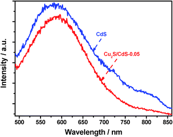 |
| | Fig. 7 PL spectra of CdS and Cu2S/CdS-0.05. The excitation wavelength was 420 nm. | |
3.4 Photocatalytic hydrogen production
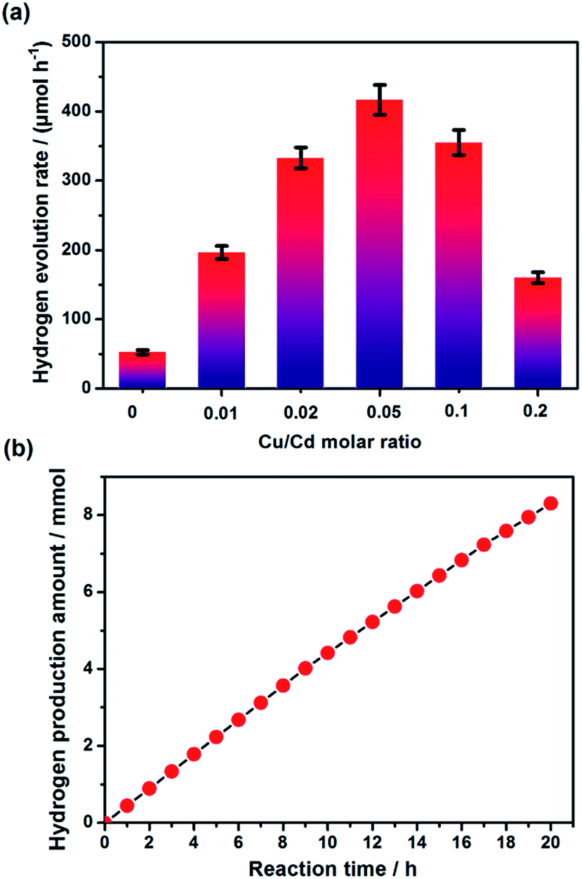
Photocatalytic performances of as-prepared samples for hydrogen production are displayed in Fig. 8a. The photocatalytic activity of single CdS was 50.1 μmol h−1. Cu2S deposition could improve the photocatalytic hydrogen production efficiently. When the loading amount of Cu2S was gradually increased, the photocatalytic activity was firstly increased and then decreased. With the optimal Cu/Cd molar ratio of 0.05, the hydrogen production rate of Cu2S/CdS was 400.1 μmol h−1, which was nearly 8 times higher than that of single CdS. The apparent quantum yield of Cu2S/CdS-0.05 at 420 nm was calculated to be 9.5%. When the Cu/Cd molar ratio was below 0.05, the increased Cu2S amount could lead to higher photocatalytic hydrogen production. However, as the Cu/Cd molar ratio exceeded 0.05, the surface of CdS polyhedrons was nearly covered by Cu2S nanoparticles (Fig. 3e and f), which may affect the efficient utilization of light by CdS photocatalysts. Meanwhile, more Cu2S nanoparticles tended to aggregate together (Fig. 3e and f), which could lead to the increased recombination of photoexcited charges at Cu2S nanoparticles. Therefore, the photocatalytic activity was gradually decreased when excess Cu2S was deposited. The photocatalytic performance of pure Cu2S was also studied. However, no hydrogen could be detected, possibly resulting from the low charge separation efficiency in Cu2S nanoparticles.41 Long-time photocatalytic test of Cu2S/CdS-0.05 sample for hydrogen production was carried out to evaluate the stability of Cu2S/CdS hybrid photocatalysts. As shown in Fig. 8b, there was no apparent decrease in the photocatalytic activity over the 20 hours' reaction, indicating the good stability of Cu2S/CdS-0.05. In order to further investigate the stability of Cu2S on the surface of CdS, we carried out the XPS measurement to study the valance state of Cu2S/CdS-0.05 sample after long-time photocatalytic reaction. It was noted in Fig. S4† that the observed Cu 2p peaks of Cu2S/CdS-0.05 sample before and after long-time photocatalytic reaction were at the same positions, revealing the good stability of Cu2S in Cu2S/CdS during the photocatalytic reaction.
 |
| | Fig. 8 (a) Photocatalytic hydrogen production over Cu2S/CdS hybrid photocatalysts with different Cu/Cd molar ratios and (b) long-time photocatalytic test of Cu2S/CdS-0.05 sample for hydrogen production. Reaction conditions: 0.2 g of CdS photocatalyst; appropriate amount of Cu2S deposited by the in situ method; 190 mL of aqueous solution containing 0.25 M Na2SO3/0.35 M Na2S; 300 W Xe lamp equipped with a cutoff filter (λ ≥ 420 nm). | |
As analysed from the PL results of CdS and Cu2S/CdS photocatalysts (Fig. 7), Cu2S deposition could lead to the more efficient charge separation in CdS, which was considered to be the key factor for the improved activity of Cu2S/CdS. The schematic diagram of the charge separation process in Cu2S/CdS could be illustrated in Fig. 9. As mentioned above, CdS and Cu2S are respectively n-type and p-type semiconductors. Meanwhile, as shown in Fig. S5,† a negative slope of the linear region in the Mott–Schottky plot of Cu2S film indicated the p-type semiconductor character of Cu2S.27 When n-type CdS polyhedrons were coupled with p-type Cu2S nanoparticles, large amounts of nanoscale p–n junctions could be generated between the two semiconductors (Fig. 5). Across the p–n junction a built-in electric field is formed, where the p-type Cu2S region is negatively charged, and the n-type CdS region is positively charged (Fig. 9a). Considering the band structures of Cu2S and CdS, it has been reported that both the conduction band (CB) and the valance band (VB) of Cu2S are higher than those of CdS.25,42 When Cu2S and CdS formed p–n heterojunction, the electron transfer occurred from Cu2S to CdS while the hole transfer occurred from CdS to Cu2S due to the different Fermi levels until the system attained equilibration. The proposed band profile for Cu2S/CdS heterojunction was shown in Fig. 9b.24,43
 |
| | Fig. 9 (a) The schematic diagram of forming p–n junction and charge transfer process in Cu2S/CdS and (b) the band structure for Cu2S/CdS heterojunction and charge separation process under illumination. | |
When Cu2S/CdS hybrid photocatalysts were irradiated with visible light, the photoexcited electrons and holes would be both obtained in CdS and Cu2S. As a result of the built-in electric field, the photogenerated electrons in the CB of Cu2S would diffuse into the CB of CdS through the p–n junction, giving rise to the accumulation of photogenerated electrons in the CdS nanocrystal. Likewise, the photogenerated holes in the VB of CdS would diffuse into the VB of Cu2S, leading to the accumulation of photogenerated holes in the Cu2S nanoparticle. As a consequence, the efficient charge separation was successfully achieved by the nanoscale p–n junctions in Cu2S/CdS. Meanwhile, The close interaction between CdS and Cu2S (Fig. 5b) could facilitate the charge transfer.44 Subsequently, the accumulated electrons would transfer to the surface of CdS to reduce H+ for hydrogen production, and the accumulated holes would transfer to the surface of Cu2S to oxidize the sacrificial reagents (S2−, SO32−). The improved photocatalytic activity was acquired through the efficient charge separation. During the photocatalytic reaction, Cu2S nanoparticles captured the photogenerated holes in CdS and functioned as the active sites for the surface oxidation reaction.
Although the charge separation could be achieved for Cu2S/CdS with different Cu/Cd molar ratios through the nanoscale p–n junctions, the efficiency of charge separation was not the same. As the Cu/Cd molar ratio is below 0.05, Cu2S nanoparticles were uniformly dispersed on the surface of CdS polyhedron. More nanoscale p–n junctions could be generated with the increased Cu2S nanoparticles deposited, resulting in higher charge separation efficiency and better photocatalytic performance. However, when the Cu/Cd molar ratio was above 0.05, the aggregation of Cu2S nanoparticles occurred, which restricted the formation of more p–n junctions. Meanwhile, the grain boundaries of Cu2S nanoparticles would act as the recombination centers, leading to lower charge separation efficiency.45 Further increasing the amount of Cu2S would give rise to the decreased photocatalytic activity.
Single Cu2S could not produce hydrogen possibly owing to its low charge separation efficiency. However, in Cu2S/CdS hybrid photocatalysts, the efficient charge separation from nanoscale p–n junctions was achieved, which could promote the utilization of photoexcited charges in Cu2S for photocatalytic reaction. This result implied that more visible light could be harvested by Cu2S/CdS for photocatalytic hydrogen production compared to single CdS, which should also contribute to the enhanced activity.
In order to demonstrate whether p-type Cu2S can enhance the activities of other n-type semiconductor photocatalyst. Cu2S was respectively coupled with n-type ZnIn2S4 and n-type TiO2 to generate Cu2S/ZnIn2S4 and Cu2S/TiO2 hybrid photocatalysts with p–n junction heterostructures. The photocatalytic hydrogen production of different photocatalysts with and without Cu2S were tested. The detailed synthesis and photocatalytic process of Cu2S/ZnIn2S4 and Cu2S/TiO2 photocatalysts can be found in the ESI.† As shown in Table 1, the hydrogen production rates of single ZnIn2S4 and TiO2 were rather low. After loading Cu2S, both photocatalytic activities were apparently improved. This result indicated that Cu2S was suitable for various photocatalysts. No matter the photocatalyst is either metal sulfide or metal oxide, Cu2S could efficiently promote the photocatalytic hydrogen production. The nanoscale p–n junctions between p-type Cu2S and n-type semiconductor, leading to more efficient charge separation, are considered to be the key factor for the improved activities. The present study thus provides a general strategy to develop efficient Cu2S-modified photocatalysts by forming p–n junction structure.
Table 1 Photocatalytic hydrogen production of different photocatalysts with and without Cu2S
| Sample |
Hydrogen production rate without Cu2S |
Hydrogen production rate with Cu2S |
| ZnIn2S4 |
5.0 μmol h−1 |
30.9 μmol h−1 |
| TiO2 |
0.5 μmol h−1 |
16.0 μmol h−1 |
4. Conclusions
In summary, Cu2S/CdS heterostructure was successfully synthesized by the in situ deposition of Cu2S onto CdS photocatalysts. Cu2S nanoparticles were tightly attached on the surface of polyhedral CdS nanocrystals in Cu2S/CdS, which led to the formation of nanoscale p–n junctions between p-type Cu2S nanoparticles and n-type CdS polyhedrons. Cu2S deposition could apparently improve the photocatalytic hydrogen production of CdS photocatalysts. The generated nanoscale p–n junctions in Cu2S/CdS, leading to the enhanced charge separation efficiency and better utilization of visible light, were considered to be the key factor for the significantly enhanced property. The photocatalytic hydrogen production of Cu2S/CdS photocatalysts was related with the Cu/Cd molar ratio. With the optimal Cu/Cd molar ratio of 0.05, the apparent quantum yield of Cu2S/CdS at 420 nm reached 9.5%. P-type Cu2S could also improve the photocatalytic activities of n-type ZnIn2S4 and n-type TiO2 by forming efficient p–n junction structure, indicating the general applicability of p-type Cu2S. This work not only demonstrates that low-price and environment-friendly p-type Cu2S could promote the photocatalytic activities of various n-type semiconductor photocatalysts but also proposes an effective guidance to developing efficient noble-metal-free hybrid photocatalysts by forming p–n junction structure.
Acknowledgements
The authors thank the financial support from the National Natural Science Foundation of China (nos 51323011 and 51236007) and the grant support from the China Postdoctoral Science Foundation (no. 2014M560768).
References
- X. Chen, S. Shen, L. Guo and S. Mao, Chem. Rev., 2010, 110, 6503 CrossRef CAS PubMed.
- K. Shimura and H. Yoshida, Energy Environ. Sci., 2011, 4, 2467 CAS.
- K. Maeda and K. Domen, J. Phys. Chem. Lett., 2010, 1, 2655 CrossRef CAS.
- J. Yang, D. Wang, H. Han and C. Li, Acc. Chem. Res., 2013, 46, 1900 CrossRef CAS PubMed.
- Y. H. Li, J. Xing, Z. J. Chen, Z. Li, F. Tian, L. R. Zheng, H. F. Wang, P. Hu, H. J. Zhao and H. G. Yang, Nat. Commun., 2013, 4, 2500 Search PubMed.
- C. Kong, S. Min and G. Lu, Chem. Commun., 2014, 50, 9281 RSC.
- Z. Xong, H. Yan, G. Wu, G. Ma, F. Wen, L. Wang and C. Li, J. Am. Chem. Soc., 2008, 130, 7176 CrossRef PubMed.
- X. Zong, J. Han, G. Ma, H. Yan, G. Wu and C. Li, J. Phys. Chem. C, 2011, 115, 12202 CAS.
- W. Zhang, Y. Wang, Z. Wang, Z. Zhong and R. Xu, Chem. Commun., 2010, 46, 7631 RSC.
- L. Zhang, T. Xie, D. Wang, S. Li, L. Wang, L. Chen and Y. Lu, Int. J. Hydrogen Energy, 2013, 38, 11811 CrossRef CAS PubMed.
- L. Ma, F. Li, Z. Sun, M. Liu, Y. Wang and L. Xu, RSC Adv., 2014, 4, 21369 RSC.
- M. Tabata, K. Maeda, T. Ishihara, T. Minegishi, T. Takata and K. Domen, J. Phys. Chem. C, 2010, 114, 11215 CAS.
- L. Zhang, B. Tian, F. Chen and J. Zhang, Int. J. Hydrogen Energy, 2012, 37, 17060 CrossRef CAS PubMed.
- P. Gomathisankar, K. Hachisuka, H. Katsumata, T. Suzuki, K. Funasaka and S. Kaneco, Int. J. Hydrogen Energy, 2013, 38, 8625 CrossRef CAS PubMed.
- J. Xu, Y. Li and S. Peng, Int. J. Hydrogen Energy, 2015, 40, 353 CrossRef CAS PubMed.
- Y. Chen and L. Guo, J. Mater. Chem., 2012, 22, 7507 RSC.
- F. Meng, J. Li, S. K. Cushing, M. Zhi and N. Wu, J. Am. Chem. Soc., 2013, 135, 10286 CrossRef CAS PubMed.
- A. J. Frank and K. Honda, J. Phys. Chem., 1982, 86, 1933 CrossRef CAS.
- A. Serpi, J. Phys. D: Appl. Phys., 1976, 9, 1881 CrossRef CAS.
- B. C. O'Regan and F. Lenzmann, J. Phys. Chem. B, 2004, 108, 4342 CrossRef.
- J. Lin, J. Shen, R. Wang, J. Cui, W. Zhou, P. Hu, D. Liu, H. Liu, J. Wang, R. I. Boughton and Y. Yue, J. Mater. Chem., 2011, 21, 5106 RSC.
- J. Zhang, S. Z. Qiao, L. Qi and J. Yu, Phys. Chem. Chem. Phys., 2013, 15, 12088 RSC.
- Z. Zhuang, Q. Peng, B. Zhang and Y. Li, J. Am. Chem. Soc., 2008, 130, 10482 CrossRef CAS PubMed.
- W. D. Gill and R. H. Bube, J. Appl. Phys., 1970, 41, 3731 CrossRef CAS PubMed.
- Y. Wu, C. Wadia, W. Ma, B. Sadtler and A. P. Alivisatos, Nano Lett., 2008, 8, 2551 CrossRef CAS PubMed.
- C. Pan, S. Niu, Y. Ding, L. Dong, R. Yu, Y. Liu, G. Zhu and Z. L. Wang, Nano Lett., 2012, 12, 3302 CrossRef CAS PubMed.
- Y. Bessekhouad, R. Brahimi, F. Hamdini and M. Trari, J. Photochem. Photobiol., A, 2012, 248, 15 CrossRef CAS PubMed.
- Y. Zhao and C. Burda, Energy Environ. Sci., 2012, 5, 5564 CAS.
- Y. Liang, M. Shao, L. Liu, J. G. McEvoy, J. Hu and W. Cui, Catal. Commun., 2014, 46, 128 CrossRef CAS PubMed.
- Y. Li, Y. Hu, S. Peng, G. Lu and S. Li, J. Phys. Chem. C, 2009, 113, 9352 CAS.
- Z. Li, H. Yang, Y. Ding, Y. Xiong and Y. Xie, Dalton Trans., 2006, 149 RSC.
- J. Liu and D. Xue, Adv. Mater., 2008, 20, 2622 CrossRef CAS.
- M. Yan, C. Chen, N. Zhang, X. Wen, W. Guo and C. Lin, Adv. Energy Mater., 2014, 4, 1301564 Search PubMed.
- Y. Liu, Y. Deng, Z. Sun, J. Wei, G. Zheng, A. M. Asiri, S. B. Khan, M. M. Rahman and D. Zhao, Small, 2013, 9, 2702 CrossRef CAS PubMed.
- J. Zhang, J. Yu, Y. Zhang, Q. Li and J. R. Gong, Nano Lett., 2011, 11, 4774 CrossRef CAS PubMed.
- D. Jing and L. Guo, J. Phys. Chem. B, 2006, 110, 11139 CrossRef CAS PubMed.
- Y. Lin, J. Zhang, E. H. Sargent and E. Kumacheva, Appl. Phys. Lett., 2002, 81, 3134 CrossRef CAS PubMed.
- Y. Wang, G. Meng, L. Zhang, C. Liang and J. Zhang, Chem. Mater., 2002, 14, 1773 CrossRef CAS.
- J. Hou, C. Yang, Z. Wang, S. Jiao and H. Zhu, RSC Adv., 2012, 2, 10330 RSC.
- J. G. Radich, N. R. Peeples, P. K. Santra and P. V. Kamat, J. Phys. Chem. C, 2014, 118, 16463 CAS.
- B. Wang, W. An, L. Liu, W. Chen, Y. Liang and W. Cui, RSC Adv., 2015, 5, 3224 RSC.
- X. Li, H. Shen, S. Li, J. Z. Niu, H. Wang and L. S. Li, J. Mater. Chem., 2010, 20, 923 RSC.
- G. L. Lazarev, J. Appl. Phys., 1980, 51, 4257 CrossRef CAS PubMed.
- X. Wang, G. Liu, Z. G. Chen, F. Li, L. Wang, G. Q. Lu and H. M. Cheng, Chem. Commun., 2009, 3452 RSC.
- S. C. Riha, R. D. Schaller, D. J. Gosztola, G. P. Wiederrecht and A. B. F. Martinson, J. Phys. Chem. Lett., 2014, 5, 4055 CrossRef CAS.
Footnote |
| † Electronic supplementary information (ESI) available: The detailed synthesis and photocatalytic process of Cu2S/ZnIn2S4 and Cu2S/TiO2 photocatalysts; the calculation method of the number of incident photons; the Cu/Cd molar ratios determined by EDX of different Cu2S/CdS samples; the schematic diagram of the photocatalytic reactor for hydrogen production; XRD patterns of CuxS (Na2S) sample and Cu2S (Na2SO3/Na2S) sample (Cu2S achieved by adding Cu2+ into Na2SO3/Na2S solution); illustration of the deposition process of Cu2S nanoparticles on CdS polyhedrons; Cu 2p XPS spectra of Cu2S/CdS-0.05 sample before and after long-time photocatalytic reaction; Mott–Schottky plot of Cu2S film. See DOI: 10.1039/c5ra00091b |
|
| This journal is © The Royal Society of Chemistry 2015 |
Click here to see how this site uses Cookies. View our privacy policy here.