
 Open Access Article
 This Open Access Article is licensed under a
 Creative Commons Attribution 3.0 Unported Licence
Correlative spectroscopy mapping of the prospective photovoltaic material bournonite using Raman and cathodoluminescence†
O. M.
Rigby
 *a,
C.
Hill
b,
G.
Kusch
c,
M.
Guennou
b,
M.
Szablewski
a,
R. A.
Oliver
c,
L.
Wirtz
b,
P.
Dale
b and
B. G.
Mendis
*a
*a,
C.
Hill
b,
G.
Kusch
c,
M.
Guennou
b,
M.
Szablewski
a,
R. A.
Oliver
c,
L.
Wirtz
b,
P.
Dale
b and
B. G.
Mendis
*a
aDepartment of Physics, Durham University, South Road, Durham, DH1 3LE, UK. E-mail: oliver.rigby@northumbria.ac.uk; b.g.mendis@durham.ac.uk
bDepartment of Physics and Materials Science, University of Luxembourg, 162a avenue de la Faïencerie, L-1511 Luxembourg, Luxembourg
cDepartment of Materials Science and Metallurgy, University of Cambridge, Charles Babbage Road, Cambridge, CB3 0FS, U.K
First published on 22nd April 2025
Abstract
The polar material bournonite (CuPbSbS3) is of interest as a new absorber layer for thin-film photovoltaics. At present, efficiencies are low and there is a lack of fundamental knowledge on the structural and optoelectronic properties of the material in thin-film form. In this study, we report complete experimental Raman spectra, which are interpreted with the help of ab initio calculations. Raman maps reveal variation of relative peak intensities both within grains and across grains as most likely caused by crystal anisotropy. We also present correlated hyperspectral cathodoluminescence (CL) results and observe a red shift of the CL peak wavelength of 5 to 15 nm at the bournonite grain boundaries. Transmission electron microscopy reveals Cu enrichment along grain boundaries that, together with CuPb antisite and interstitial Cu point defect formation, is proposed to cause the luminescence red shift.
1. Introduction
Bournonite (CuPbSbS3) was identified as a potential absorber layer for thin-film photovoltaics in a theoretical study by Wallace et al.,1 which searched for polar minerals with band gaps suitable for single-junction solar cells. Bournonite is orthorhombic and belongs to the space group Pmn21. The resultant non-centrosymmetric unit cell leads to a net electric dipole moment and, based on theoretical work,1 bournonite can be classified as a (weakly) ferroelectric photovoltaic material (or photoferroic). Photoferroics have a potential advantage over traditional thin-film photovoltaic materials, as the internal electric field due to polarisation may aid charge separation, leading to an improved open circuit voltage (VOC). Bournonite has favourable optical properties including a band gap of ∼1.3 eV1–3 and a large absorption coefficient (∼104 cm−1 to 105 cm−1).4 Additionally, it has previously been shown through density functional theory (DFT) calculations that bournonite is defect-tolerant.4 Although the ferroelectric nature of bournonite has not been directly confirmed, recent experimental work has shown that observed domain walls do not contribute to Shockley–Read–Hall recombination of charge carriers or block charge carrier transport.5 Various techniques have been used to synthesise bournonite, including those suitable for nanocrystals6 and thin-films2–4,7 as well as through solid-state bulk powder reactions.8–10 The record efficiency for a bournonite solar cell is currently 2.65%,2 where the device was fabricated in a superstrate architecture, with TiO2, spiro-OMeTAD, fluorine-doped tin oxide (FTO), and gold contacts. Limitations to efficiency improvements were highlighted to be the grain sizes attainable and morphological quality of the thin-film.In this work, we use the experimental techniques of Raman spectroscopy, cathodoluminescence (CL) spectroscopy, and transmission electron microscopy (TEM) to examine thin-films of bournonite. Raman spectroscopy has been used in other photovoltaic absorbers to determine, for example, secondary phases,11 doping concentrations through peak broadening,12 and to uncover order–disorder transitions.13 Order–disorder transitions occur when there is a structural change to the material due to a change in temperature, as occurs in the photovoltaic absorber Cu2ZnSnS4 (CZTS). For CZTS the order–disorder transition results in CuZn and ZnCu antisites that are thought to contribute to a VOC deficit.14,15 Evidence from Raman spectroscopy for the order–disorder transition can be peak broadening, changes to the relative peak intensities, or the presence of additional peaks.13,14 The Raman spectra reported so far for bournonite are of a limited range of wavenumbers and with broad peaks,3,7 while no luminescence measurements (i.e. photo-, electro- or cathodo-) of bournonite have been reported. As such, this work aims to use these techniques to evaluate the quality of thin-films of bournonite and to give insight into correlations between the optoelectronic properties and the underlying structure. From this study we determine the role of crystal anisotropy on Raman peak intensities in bournonite, confirm a previously unreported secondary phase tetrahedrite (Cu12Sb4S13), as well as detect a red shift of the CL peak at the grain boundaries relative to the grain interiors, which is caused by Cu enrichment at the grain boundaries.
2. Experimental and computational details
Thin bournonite films were prepared using a thiol–amine solution, following a methodology similar to that of Koskela et al.3 The chosen masses conform to stoichiometric bournonite and for the synthesis, 29.7 mg copper (II) oxide (CuO), 77.7 mg lead (II) oxide (PbO) and 67.5 mg antimony (III) sulfide (Sb2S3) were combined in a round-bottom flask with 0.8 mL 1,2-ethylenediamine (C2H4 (NH2)2) and 0.2 mL 1,2-ethanedithiol (C2H4 (SH)2). The mixture was stirred on a hot plate at ∼25 °C for over 12 hours resulting in a fluid brown solution. 2.5 cm2 soda lime glass substrates were sequentially scrubbed with decon-90 and deionised water before they were sonicated in deionised water twice, acetone and isopropanol for 15 minutes each with drying by a N2 gun in between each sonication. The ink was deposited on the cleaned glass slides by spin coating using a Laurell WS-400B-6NPP/Lite spin coater at 3000 rpm and with 60 μL of solution per coat. After spin coating, the samples were annealed in a tube furnace at a range of temperatures from 400 °C to 500 °C for 1 hour under flowing N2.X-ray diffraction (XRD) measurements were performed using a Bruker D8 Advance X-ray Diffractometer and Cu Kα source. Rietveld refinement was performed using General Structure Analysis Software (GSAS) II.16 Raman measurements were performed at the Luxembourg Institute of Science and Technology (LIST) using a Renishaw InVia Raman microscope using both a 633 nm laser and 785 nm laser. The 633 nm laser with 43 μW power and 1 μm spot size was used for single point high resolution spectra, with each spectrum the result of 60 exposures of the sample to the laser for a time of 60 s each. The 785 nm laser with 87 μW power and 1 μm spot size was used for the Raman maps. The Raman was performed at a magnification of 100× with a numerical aperture of 0.9. Each point spectrum in the map is the result of 10 exposures to 60 s of laser. Data analysis of the Raman map data was performed using Gatan Digital Micrograph software. CL measurements were done at the University of Cambridge using an Attolight Allalin 4027 Chronos scanning electron microscope (SEM) operating at 8 kV and at room temperature. For data analysis of the CL measurements, Hyperspy-CL-v3 was used, an adapted version of Hyperspy which is an open-source Python library.17 To prepare cross-sections for TEM, a Helios 600 focused ion beam microscope (FIB) was used at Durham University using a Ga ion beam. TEM, scanning transmission electron microscopy (STEM) and energy-dispersive X-ray analysis (EDX) were done at Durham University using a JEOL 2100F field emission gun transmission electron microscope operating at 200 kV using an Oxford Instruments X-Max 65T silicon drift detector. Secondary electron (SE) imaging and EDX chemical analysis was also performed in a Hitachi SU70 SEM operating at 10 kV.
Ab initio calculations were performed using density functional theory (DFT) using the quantum ESPRESSO (QE) package18 with the Perdew–Burke–Ernzerhof (PBE) exchange–correlation functional (XC).19 We used scalar-relativistic norm-conserving pseudopotentials from the PseudoDojo project.20 We performed structural relaxation imposing the experimental lattice constants a = 7.79 Å, b = 8.15 Å, and c = 8.69 Å employing 4 × 4 × 4 k-point sampling and an energy cutoff at 100 Ry. We then used density-functional perturbation theory (DFPT)21 for the calculation of phonons at Γ (wave vector q = 0). We calculated the non-resonant Raman spectrum at 300 K using the implementation of Lazzeri and Mauri22 for the Raman tensor. This implementation is currently only for the local-density approximation (LDA), so we used LDA to calculate the Raman tensor but kept the phonon frequencies and eigenvectors calculated with the PBE functional. In parallel, we performed calculations of the Raman spectra using DFT with Gaussian orbitals as implemented in the CRYSTAL17 code.23–25 This gives similar results (see ESI†), but due to uncertainties in the convergence of basis sets, we present the calculations using plane waves in the main text. We also note that our calculations are in close agreement with the entry on bournonite in a recent high-throughput data base of non-resonant Raman spectra.26
3. Results and discussion
Plan-view and cross-section secondary electron (SE) images of the thin-films annealed at different temperatures are shown in Fig. S1 (ESI†). Fig. S2 (ESI†) presents comparative histograms of grain sizes for samples annealed at 450 °C and 500 °C, where the average grain size increases from (0.39 ± 0.01) μm to (2.14 ± 0.06) μm with annealing temperature. This work focused on bournonite thin films which had been annealed at 500 °C, due to its large grain size which enabled grain to grain spectroscopy.XRD was performed to determine the phases present in the 500 °C sample. Rietveld refinement (Fig. 1) confirmed the sample to be composed of primarily bournonite with minor secondary phase peaks as denoted by asterisks. Possible candidates for these peaks include PbS or Sb2S3, which are commonly reported for the synthesis of bournonite.3,7 We have also explored the possibility of tetrahedrite (Cu12Sb4S13) which was observed (see below) but which also cannot be assigned to the secondary phase peak locations. The Rietveld refinement had a weighted profile residual of Rwp = 4.52%, indicative of an excellent fit. The bournonite lattice parameters were a = 7.81 Å, b = 8.15 Å, and c = 8.70 Å.
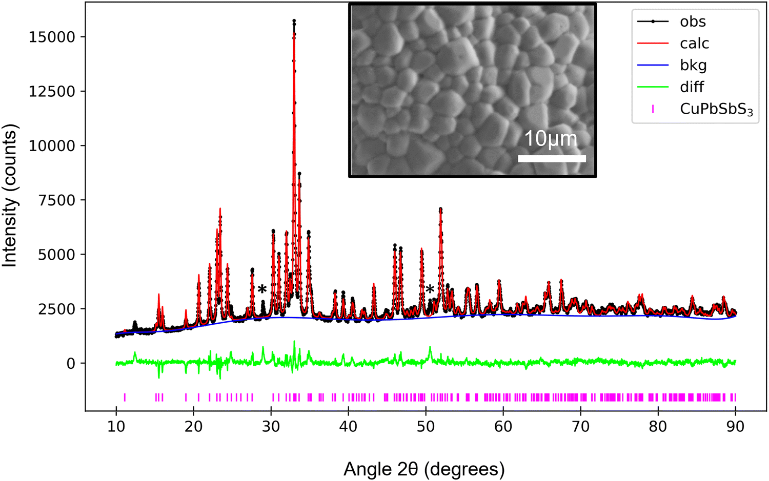 | ||
| Fig. 1 X-ray diffraction for the 500 °C thin-film sample, Rietveld refined using a pure bournonite phase. The raw spectrum is marked by black spots (‘obs’), the refined spectrum by the red line (‘calc’) and the calculated background by the blue line (‘bkg’). Markers designating peak locations for the CuPbSbS3 phase are shown underneath the main plot. A plot of the weighted difference between the observed and calculated intensities is shown in green. Minor secondary phase reflections are marked by asterisks. The fitting results in a Rwp of 4.52%. The figure inset is a secondary electron SEM image of the thin-film grain structure. | ||
3.1. Raman
Raman spectroscopy was used to further evaluate the quality of the thin film. Raman spectra of bournonite in the literature are limited to peaks located near 320 cm−1, 290 cm−1 and 180 cm−1.3,7 A single point Raman spectrum acquired from within a grain of bournonite is presented in Fig. 2a. Low power and long acquisition times were found to be essential for obtaining high quality Raman spectra. The spectrum presented here notably covers all the peaks in the complete spectrum and the peaks are noticeably sharper than in previous reports.3,7 | ||
| Fig. 2 a) Single point Raman spectrum of bournonite with peak wavenumbers labelled. Lorentzian fits to individual peaks are shown in blue, while the red line represents the cumulative fit. (b) PBE calculated DFT Raman for polycrystalline bournonite. | ||
To identify the origin of individual Raman modes, we calculated a polycrystalline Raman spectrum (direction and polarisation averaged) for bournonite using DFT. The result is shown in Fig. 2b and reproduces the main Raman peaks observed in the experiment. The peak positions calculated using DFT are within the typical accuracy of DFT. For a discussion and estimation of the error of ab initio calculations, see the ESI.† From the DFT results, we see that most of the experimental peaks and also most of the smaller visible peaks in the calculated spectrum are modes of A1 symmetry. A full list of all peaks and their symmetry classification is presented in the ESI† where we also show sketches of the phonon modes that give rise to the most intense Raman peaks. The low wavenumber peaks up to 111 cm−1 can be attributed to combined vibrations of all atoms in the lattice, whereas the higher modes consist mostly of vibrations of the lighter S atoms: the 178 cm−1 and 200 cm−1 modes are due to Pb–S stretching (with associated Cu–S–Sb bending) and the 294 cm−1, 326 cm−1 and 338 cm−1 peaks are related to Sb–S stretching. Although DFT indicated that additional peaks should be present, these are not resolved experimentally because of their proximity to more intense peaks and because of some noise in the experimental data.
A Raman map of a region of bournonite revealed the presence of a single grain of tetrahedrite (Cu12Sb4S13) as labelled in Fig. 3a. A single point Raman spectrum of the tetrahedrite grain is shown in Fig. 4a, and is consistent with previous results.27 EDX mapping in the SEM also confirmed local Cu enrichment and Pb, S depletion at the Cu12Sb4S13 tetrahedrite grain, relative to the CuPbSbS3 bournonite matrix (Fig. S3, ESI†). Tetrahedrite is a previously unreported secondary phase in the synthesis of bournonite; the more common secondary phases PbS and Sb2S3 were not detected anywhere in this sample using Raman spectroscopy.
 | ||
Fig. 3 a) SE image of the area mapped by Raman (red box) with locations of extracted point spectra and the Cu12Sb4S11 tetrahedrite grain labelled. (b) Map of the 326 cm−1 peak and (c) 74 cm−1 peak intensity. (d) Map of  intensity ratio. intensity ratio. | ||
 | ||
| Fig. 4 Raman spectra for individual points labelled in Fig. 3a. (a) Raman spectrum extracted from the tetrahedrite grain. (b) Intra-grain Raman spectra from points ‘A’ and ‘B’. (c) Inter-grain Raman spectra from points ‘C’ and ‘D’. (d) Polarised Raman spectra acquired from point ‘D’ in parallel and crossed polarisation conditions. | ||
There was no broadening or shifting of the bournonite peaks observed across the Raman map, but there was variation in the relative intensities of the 74 cm−1 and 326 cm−1 peaks, as well as more subtle changes between the 74 cm−1 and 294 cm−1 relative peak intensities. To help determine if this was related to possible order–disorder effects or due to anisotropy of the grains, an intensity ratio Q was defined: 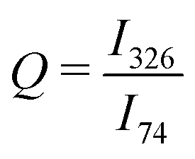 , where Ix is the intensity of the peak at wavenumber x. Maps of the intensities I326 and I74 and Q intensity ratio are shown in Fig. 3b–d, respectively. While the tetrahedrite grain and the large bournonite grain labelled ‘D’ in Fig. 3a can be distinguished there are no other clear morphological features resulting from these maps. To further investigate the spatial variation in relative peak intensity, point spectra were extracted from two crystal facets of the same grain (points ‘A’ and ‘B’ in Fig. 3a) and two separate grains (points ‘C’ and ‘D’). These point spectra are shown in Fig. 4 and indicate that the value of Q changes for both cases. Given that Q is relatively unchanged for the large grain ‘D’, which does not exhibit any well-defined crystal facets, but has variation for points ‘A’ and ‘B’, suggests the change in Q-value can be attributed to crystal anisotropy. However, applying a polarisation filter to the laser source and detector did not show any significant changes to the 74 cm−1, 294 cm−1 or 326 cm−1 peaks for a point spectrum acquired from grain ‘D’, though some changes to the peaks lower than 100 cm−1 were present, as shown in Fig. 4d. DFT calculations (Fig. S9, ESI†) show that for a polycrystalline sample the isotropic intensity ratios for Q change from ∼4 for the parallel components to ∼1 for the perpendicular components. Polarised Raman of a bournonite single crystal oriented along the unit cell axes has been shown by Kharbish et al.28 to affect the relative intensities of the 294 cm−1 and 326 cm−1 peaks, in agreement with the DFT calculations. Although the polarised Raman spectra in Fig. 4d did not show the variation expected, this is likely due to the particular grain chosen. For example, the grain may be oriented along a high index (low symmetry) crystal direction where anisotropic effects are suppressed, or the crystal orientation may be continuously changing due to grain curvature. Furthermore, point Raman spectra acquired from a bulk synthesised and naturally occuring mineral of bournonite did show the expected changes with polarisation (Fig. S4, ESI†). Therefore, anisotropy is likely to be the dominant cause for the variation in Q-values across the mapped region, and consequently no information can be extracted about potential structural disorder in the material.
3.2. Cathodoluminescence
CL hyperspectral mapping was performed on the same area analysed by Raman. Fig. 5 shows a secondary electron (SE) image of this area as well as the panchromatic CL (PanCL) map after the background had been removed. The morphology of the area, including all grains and grain boundaries (GBs), was clearly resolved in the PanCL map (Fig. 5c). The summed CL spectrum from the entire map area is shown in Fig. 5a; two peaks are observed at ∼675 nm and ∼989 nm. The ∼989 nm (∼1.25 eV) peak agrees with the band gap for bournonite.1–3 Applying bandpass filters to the CL hyperspectral data (Fig. 5d and e) reveals that the source of the ∼675 nm peak is the tetrahedrite grain. The bright corners in the right hand side of Fig. 5d are due to luminescence from the bare glass substrate. | ||
| Fig. 5 a) Summed CL spectrum over the mapped region, which is shown as an SE image in (b). The purple line is an asymmetric Gaussian fit with a peak centre of xc =989.2 ± 0.1 nm. The wavelengths used for the bandpass filters in maps d, e are shown as blue and red strips respectively. (c) Panchromatic CL (PanCL) map extracted from the hyperspectral data. Bandpass filtered maps of (d) tetrahedrite (670 nm to 690 nm) and (e) bournonite (978 nm to 1005 nm). The colour bar in each map is the intensity measured in counts. | ||
Gaussians were fitted to the bournonite peak wavelength range for each point in the hyperspectral map. The resulting fitting parameters, i.e. peak centre, amplitude and full width at half maximum (FWHM), are shown in Fig. 6. Apart from the tetrahedrite grain, where the quality of fit is unsurprisingly poor, there is a clear correlation of peak centre with grain morphology. In particular, the CL of the GBs is red shifted compared to the grain interiors by ∼5 nm to 15 nm (∼12 meV to 18 meV). To confirm the red shift behaviour of the GB luminescence, point spectra were extracted from multiple pixels, including large grains, GBs and some of the smaller grains. The location of some example extracted spectra is indicated in the Fig. 6b inset. Interestingly some of the smaller grains show blue shifted CL compared to the CL of the larger grain interiors. The asymmetric Gaussian amplitudes at the GBs are lower than the grain interiors, as is expected due to higher levels of non-radiative recombination of charge carriers.29 The FWHM is relatively constant across the bournonite thin-film, suggesting uniform crystal quality (e.g. Urbach tails) of the individual grains.
 | ||
| Fig. 6 a) Map of the peak centre from fitting a Gaussian to the bournonite CL peak. Colour bar denotes the peak centre wavelength in nm. (b) Select point spectra showing the variation in peak centre with sample microstructure. Inset shows the locations where the point spectra were taken. (c) Map of the amplitude of the fitted Gaussian peaks (colour bar denotes amplitude value in ‘counts’). (d) Map of the FWHM of the fitted Gaussian peaks (colour bar denotes FWHM value in nm). | ||
Red shifted luminescence at GBs has been reported before for Cu2ZnSnS4 (CZTS) on the order of 4 meV to 5 meV and Cu(In,Ga)Se2 (CIGS) on the order of 10 meV to 15 meV by Romero et al.30 The mechanism proposed for these observations was a depletion of Cu content at the GBs resulting in shallow band gap defect states. For CIGS these are VCu and InCu while for CZTS these are VCu and ZnCu, which has since been confirmed by other studies.31,32 For CZTS, intra-grain variation of the CL was suggested to be related to the order–disorder of the kesterite structure.33
3.3. Transmission electron microscopy
To further investigate the cause of the red shifted GB luminescence, a TEM sample was prepared from the same CL mapped region, with the aim to identify if there was any variation in elemental composition at the grain boundary. The GB chosen was located away from the tetrahedrite grain, so that any variation in elemental distribution is not related to tetrahedrite formation (see Fig. S5, ESI†). Fig. 7a shows a TEM bright-field (BF) image of the GB and Fig. 7b and c show high-resolution electron microscopy (HREM) images of the GB atomic structure. The TEM sample in Fig. 7b and c is oriented along the zone axis of the left-hand (LH) and right-hand (RH) grains respectively. A difference in contrast is observable between the two grains, due to the misorientation across the GB. Separate diffraction patterns (DPs) of the zone axes were taken from the LH and RH grains as shown in Fig. 7d and e respectively. The XRD Rietveld refined bournonite lattice parameters of a = 7.81 Å, b = 8.15 Å and c = 8.70 Å, which are similar to the literature values,6 were used to index the diffraction patterns. The DPs confirm that both grains are bournonite, with the LH grain oriented along [![[1 with combining macron]](https://www.rsc.org/images/entities/char_0031_0304.gif) 10] and the RH grain oriented along the [001] zone axis.
10] and the RH grain oriented along the [001] zone axis.
 | ||
| Fig. 7 a) BF image of a bournonite GB with red arrows denoting its location. (b) HREM of the GB, with the left-hand grain oriented along the [10] zone axis (c). HREM of the GB, with the right-hand grain oriented along the [001] zone axis. DP from the (d) LH side and (e) RH side of the GB with planes indexed. | ||
A STEM EDX map of the GB is presented in Fig. 8, with elemental maps for Cu, Pb, Sb and S. The region of darker contrast at the GB triple point (top region of EDX map) is shown to be rich in Pb and S. A DP of this region (see Fig. S6, ESI†) was indexed to be PbS. Another feature suggested by the EDX mapping is an increase in Cu along the GB. To elucidate the distribution of the elements at the GB, multiple linescans were taken across the GB, one of which is shown in Fig. 8b. The linescan confirms the GB to be Cu-rich, as evidenced by the sharp increase in Cu. Additionally the linescan also suggests a decrease in Pb and S along the GB. Similar trends were observed for the other linescans as well (Fig. S7, ESI†). It is proposed that the formation of the Pb, S-rich PbS phase at the GB triple point in bournonite has resulted in Cu-enrichment along the GB. Density functional theory (DFT) calculations by Liu et al.4 suggest shallow band gap defect states of CuPb and Cui (interstitial Cu) to have low formation enthalpies for a perfect crystal of bournonite. These defects are consistent with the Cu enrichment at the GB and are likely responsible for the change in CL peak centre seen at the GBs. To reduce Cu diffusion at GBs it may be necessary to anneal films at lower temperatures, though this will limit the grain size. It may then be beneficial to introduce dopants such as Se, Na or Li which have been successful for other chalcogenides at improving grain growth.34–36
 | ||
| Fig. 8 (a) Bright-field image of the bournonite GB with EDX linescan location (dashed line) and mapped region (red box) annotated. (b) EDX linescan and elemental mappings for (c)–(f) Cu, Pb, Sb and S. The white bar indicates a scale of 100 nm for all images. | ||
As well as GBs and secondary phases, other planar defects were also found in this thin-film sample, as seen in Fig. 9a. The HREM image (Fig. 9b) shows sharp crystallographic boundaries for the planar defect and the corresponding DP (Fig. 9c) shows ‘spot splitting’, indicative of a twin boundary. This is confirmed by the mirror symmetry of [001] crystal directions within grains either side of the planar defect (Fig. 9b). Bournonite is a ferroelectric material with polarisation oriented along [001]. The switching of the [001] direction indicates this planar defect is a ferroelectric domain wall. Domain walls of this nature have been reported before by Rigby et al.,5 and were found not to affect the recombination properties of bournonite or to block charge carrier transport. Their effect on photovoltaic device performance is therefore benign.
 | ||
| Fig. 9 (a) BF image showing a GB extending vertically along the bournonite film thickness, and twin boundaries to the bottom left (locations annotated by red arrows) (b) HREM image of the end-on twin boundaries. Red arrows indicate the [001] crystal direction either side of the twin boundary. (c) [100] zone axis DP acquired over the twin boundary showing spot splitting (such as those circled). | ||
4. Conclusions
Thin-film bournonite has been investigated through a correlated study of Raman, CL spectroscopy and TEM. Complete Raman spectra have been reported for the first time and DFT calculations confirm the major experimental peak positions. Raman maps revealed the presence of a tetrahedrite secondary phase, as well as variations in the relative intensities for the 74 cm−1 and 326 cm−1 peaks in the bournonite matrix. Raman maps, extracted point spectra, polarised Raman spectroscopy and DFT indicate that this variation is most likely due to anisotropy of the grains rather than any structural disorder. CL of the bournonite shows that the luminescence at the GBs is red shifted compared to the grain interiors. TEM revealed the presence of a PbS secondary phase at the intersection of the GB with the specimen surface. Additionally Cu enrichment at the GB is observed and this is proposed to have been driven by the formation of the PbS grain. A higher concentration of low energy point defects, such as CuPb and Cui, is therefore believed to be the origin of the CL red shift at the GBs. The small GB red shift (12 meV to 18 meV) observed by CL suggests these point defects have shallow energy levels within the band gap. Consequently Cu-enrichment at the grain boundaries is not expected to significantly increase Shockley–Read–Hall recombination above that of a chemically pure grain boundary in bournonite. Hence the grain boundary segregation observed here should not adversely affect thin-film photovoltaic device performance metrics. Further, given the p-type nature of bournonite is due to CuPb, it is suggested enriching bournonite with Cu to improve charge carrier separation would not have significantly detrimental non-radiative losses.Author contributions
O. M. R: conceptualization, data curation, formal analysis, investigation, visualization, writing – original draft, writing – review & editing. C. H: investigation. G. K: investigation, data curation, software, writing – review & editing. M.G: data curation, funding acquisition, resources, writing – review & editing. M.S: resources. R.A.O: funding acquisition, writing – review & editing. L.W: formal analysis, funding acquisition, investigation, software, visualization, writing – original draft, writing – review & editing. P.D: conceptualization, funding acquisition. B. G.M: conceptualization, formal analysis, funding acquisition, investigation, software, supervision, writing – original draft, writing – review & editing. All authors have revised the manuscript and have given approval to the final version of the manuscript.Data availability
The experimental data for this work is available open access from the Durham University research data repository with the DOI: 10.15128/r1k930bx10h. The input and output files of our ab initio calculations of the Raman spectrum and the files for the visualization of phonon-eigenvectors are available in the NOMAD repository with the DOI: 10.17172/NOMAD/2025.01.14-2. An interactive animation of the phonon modes (as shown in the ESI†) can be viewed here.Conflicts of interest
The authors have no conflict of interest to declare.Acknowledgements
This work was financially supported by the U.K. Engineering and Physical Sciences research Council (EPSRC) Centre for Doctoral Training in Renewable Energy Northeast Universities (ReNU) through grant EP/SO23836/1. R.A. Oliver and G. Kusch acknowledge EP/R025193/1. C. Hill and M. Guennou acknowledge support by the Luxembourg National Research Fund (FNR) (PRIDE/15/10935404). L.W. acknowledges funding by the FNR through project C22/MS/17415967/ExcPhon.References
- S. K. Wallace, K. L. Svane, W. P. Huhn, T. Zhu, D. B. Mitzi, V. Blum and A. Walsh, Sustainable Energy Fuels, 2017, 1, 1339–1350 RSC.
- M. Zhang, Y. Liu, B. Yang, X. Lin, Y. Lu, J. Zheng, C. Chen and J. Tang, ACS Appl. Mater. Interfaces, 2021, 13, 13273–13280 CrossRef CAS PubMed.
- K. Koskela, B. Melot and R. Brutchey, J. Am. Chem. Soc., 2020, 142, 6173–6179 CrossRef CAS PubMed.
- Y. Liu, B. Yang, M. Zhang, B. Xia, C. Chen, X. Liu, J. Zhong, Z. Xiao and J. Tang, Nano Energy, 2020, 71, 104574 CrossRef CAS.
- O. M. Rigby, T. Richards-Hlabangana, Q. M. Ramasse, I. MacLaren, R. A. Lomas-Zapata, M. S. Rumsey, K. P. McKenna and B. G. Mendis, J. Appl. Phys., 2022, 132, 185001 CrossRef CAS.
- K. Wei, J. Martin, J. R. Salvador and G. S. Nolas, Cryst. Growth Des., 2015, 15, 3762–3766 CrossRef CAS.
- Y. T. Alharbi, F. Alam, K. Parvez, M. Missous and D. J. Lewis, Inorg. Chem., 2021, 60, 13691–13698 CrossRef CAS PubMed.
- S. Bairamova, M. Bagieva, S. Agapashaeva and O. Aliev, Inorg. Mater., 2011, 47, 345–348 CrossRef CAS.
- O. Aliyev, D. Ajdarova, S. Bayramova, S. Aliyeva and V. Ragimova, Azerb. Chem. J., 2016, 2, 51–54 Search PubMed.
- Y. Dong, A. R. Khabibullin, K. Wei, J. R. Salvador, G. S. Nolas and L. M. Woods, Chem. Phys. Chem., 2015, 16, 3264–3270 CrossRef CAS PubMed.
- A. Alvarez Barragan, H. Malekpour, S. Exarhos, A. A. Balandin and L. Mangolini, ACS Appl. Mater. Interfaces, 2016, 8, 22971–22976 CrossRef CAS PubMed.
- S. Palleschi, D. Mastrippolito, P. Benassi, M. Nardone and L. Ottaviano, Appl. Surf. Sci., 2021, 561, 149691 CrossRef CAS.
- J. J. S. Scragg, L. Choubrac, A. Lafond, T. Ericson and C. Platzer-Björkman, Appl. Phys. Lett., 2014, 104, 041911 CrossRef.
- K. Rudisch, Y. Ren, C. Platzer-Björkman and J. Scragg, Appl. Phys. Lett., 2016, 108, 231902 CrossRef.
- S. K. Wallace, J. M. Frost and A. Walsh, J. Mater. Chem. A, 2019, 7, 312–321 RSC.
- B. H. Toby and R. B. Von Dreele, J. Appl. Crystallogr., 2013, 46, 544–549 CrossRef CAS.
- D. Johnstone, E. Pascal, P. Edwards and J. Ferrer Orri, Hyperspy-CL, 2022 DOI:10.5281/zenodo.1469364.
- P. Giannozzi, O. Andreussi, T. Brumme, O. Bunau, M. B. Nardelli, M. Calandra, R. Car, C. Cavazzoni, D. Ceresoli, M. Cococcioni, N. Colonna, I. Carnimeo, A. D. Corso, S. de Gironcoli, P. Delugas, R. A. DiStasio, A. Ferretti, A. Floris, G. Fratesi, G. Fugallo, R. Gebauer, U. Gerstmann, F. Giustino, T. Gorni, J. Jia, M. Kawamura, H.-Y. Ko, A. Kokalj, E. Küçükbenli, M. Lazzeri, M. Marsili, N. Marzari, F. Mauri, N. L. Nguyen, H.-V. Nguyen, A. O. De-la Roza, L. Paulatto, S. Poncé, D. Rocca, R. Sabatini, B. Santra, M. Schlipf, A. P. Seitsonen, A. Smogunov, I. Timrov, T. Thonhauser, P. Umari, N. Vast, X. Wu and S. Baroni, J. Phys.:Condens. Matter, 2017, 29, 465901 CrossRef CAS PubMed.
- J. P. Perdew, K. Burke and M. Ernzerhof, Phys. Rev. Lett., 1996, 77, 3865–3868 CrossRef CAS PubMed.
- M. van Setten, M. Giantomassi, E. Bousquet, M. Verstraete, D. Hamann, X. Gonze and G.-M. Rignanese, Comput. Phys. Commun., 2018, 226, 39–54 CrossRef CAS.
- S. Baroni, S. de Gironcoli, A. Dal Corso and P. Giannozzi, Rev. Mod. Phys., 2001, 73, 515–562 CrossRef CAS.
- M. Lazzeri and F. Mauri, Phys. Rev. Lett., 2003, 90, 036401 CrossRef PubMed.
- R. Dovesi, A. Erba, R. Orlando, C. M. Zicovich-Wilson, B. Civalleri, L. Maschio, M. Reérat, S. Casassa, J. Baima, S. Salustro and B. Kirtman, WIREs Comput. Mol. Sci., 2018, 8, e1360 CrossRef.
- L. Maschio, B. Kirtman, M. Reérat, R. Orlando and R. Dovesi, J. Chem. Phys., 2013, 139, 164101 CrossRef PubMed.
- L. Maschio, B. Kirtman, M. Reérat, R. Orlando and R. Dovesi, J. Chem. Phys., 2013, 139, 164102 CrossRef PubMed.
- M. Bagheri and H.-P. Komsa, Sci. Data, 2023, 10, 1–11 CrossRef PubMed.
- F. Ghisani, K. Timmo, M. Altosaar, J. Raudoja, V. Mikli, M. Pilvet, M. Kauk-Kuusik and M. Grossberg, Mater. Sci. Semicond. Process., 2020, 110, 104973 CrossRef CAS.
- S. Kharbish, E. Libowitzky and A. Beran, Eur. J. Mineral., 2009, 21, 325–333 CrossRef CAS.
- J. Moseley, M. M. Al-Jassim, D. Kuciauskas, H. R. Moutinho, N. Paudel, H. L. Guthrey, Y. Yan, W. K. Metzger and R. K. Ahrenkiel, IEEE J. Photovolt., 2014, 4, 1671–1679 Search PubMed.
- M. J. Romero, H. Du, G. Teeter, Y. Yan and M. M. Al-Jassim, Phys. Rev. B:Condens. Matter Mater. Phys., 2011, 84, 165324 CrossRef.
- D. Abou-Ras, S. S. Schmidt, R. Caballero, T. Unold, H.-W. Schock, C. T. Koch, B. Schaffer, M. Schaffer, P.-P. Choi and O. Cojocaru-Mirédin, Adv. Energy Mater., 2012, 2, 992–998 CrossRef CAS.
- D. Abou-Ras, B. Schaffer, M. Schaffer, S. S. Schmidt, R. Caballero and T. Unold, Phys. Rev. Lett., 2012, 108, 075502 CrossRef PubMed.
- B. Mendis, A. Taylor, M. Guennou, D. Berg, M. Arasimowicz, S. Ahmed, H. Deligianni and P. Dale, Sol. Energy Mater. Sol. Cells, 2018, 174, 65–76 CrossRef CAS.
- S. Uli
![[c with combining breve]](https://www.rsc.org/images/entities/char_0063_0306.gif) ná, L. M. Welch, A. Abbas, M. Togay, V. Tsai, T. R. Betts, A. V. Malkov, J. M. Walls and J. W. Bowers, Prog. Photovoltaics Res. Appl., 2021, 29, 546–557 CrossRef.
ná, L. M. Welch, A. Abbas, M. Togay, V. Tsai, T. R. Betts, A. V. Malkov, J. M. Walls and J. W. Bowers, Prog. Photovoltaics Res. Appl., 2021, 29, 546–557 CrossRef. - S. G. Haass, C. Andres, R. Figi, C. Schreiner, M. Bürki, Y. E. Romanyuk and A. N. Tiwari, Adv. Energy Mater., 2018, 8, 1701760 CrossRef.
- Y. Qu, G. Zoppi and N. S. Beattie, Sol. Energy Mater. Sol. Cells, 2016, 158, 130–137 CrossRef CAS.
Footnote |
| † Electronic supplementary information (ESI) available. See DOI: https://doi.org/10.1039/d5tc00630a |
| This journal is © The Royal Society of Chemistry 2025 |