
 Open Access Article
 This Open Access Article is licensed under a
 Creative Commons Attribution 3.0 Unported Licence
Alumina nanoparticles enable optimal spray-coated perovskite thin film growth on self-assembled monolayers for efficient and reproducible photovoltaics†
Elena J.
Cassella‡
a,
Robert D.J.
Oliver‡
 b,
Timothy
Thornber
a,
Sophie
Tucker
ac,
Rehmat
Goodwin
ac,
David G.
Lidzey
*a and
Alexandra J.
Ramadan
*a
b,
Timothy
Thornber
a,
Sophie
Tucker
ac,
Rehmat
Goodwin
ac,
David G.
Lidzey
*a and
Alexandra J.
Ramadan
*a
aDepartment of Physics and Astronomy, University of Sheffield, Hicks Building, Hounsfield Road, Sheffield S3 7RH, UK. E-mail: a.ramadan@sheffield.ac.uk; d.g.lidzey@sheffield.ac.uk
bDepartment of Materials Science and Engineering, University of Sheffield, Sir Robert Hadfield Building, Mappin Street, Sheffield, S1 3JD, UK
cGrantham Centre for Sustainable Futures, University of Sheffield, Sheffield S10 2TN, UK
First published on 25th July 2024
Abstract
The power conversion efficiencies of metal halide perovskite photovoltaics have increased rapidly over the past decade attracting significant academic and industrial interest. The ease with which high performance perovskite photovoltaics can be fabricated through solution processing routes has opened up significant possibilities for fabrication through existing, industrially mature high-throughput solution coating techniques such as spray-coating. The power conversion efficiencies of spray-coated metal halide perovskite photovoltaics are limited by non-radiative recombination at the interfaces with charge transport layers necessitating the implementation of new charge transport layers. The self-assembled monolayer (SAM) charge transport layers have resulted in record perovskite photovoltaic device performances, due to reduced non-radiative recombination. However, poor wettability associated with some SAMs significantly limits their applicability, this is exaggerated for droplet-based scalable technologies like spray-coating. Here we report an optimised aluminium oxide nanoparticle interlayer which enables spray-coating of triple cation metal halide perovskite thin films and devices onto Me-4PACz (([4-(3,6-dimethyl-9H-carbazol-9-yl)butyl]phosphonic acid)). Our interlayer results in improved structural and optoelectronic properties of spray-coated perovskite thin films, compared to those fabricated through spin-coating. These improved properties enable the fabrication of p–i–n photovoltaic devices with efficiencies over 20% – some of the highest reported for both spray-coated devices in p–i–n architecture, and devices having a spray-coated “triple cation” perovskite active layer.
 Alexandra J. Ramadan | Alexandra Ramadan is a Lecturer in the Department of Physics and Astronomy at the University of Sheffield. She received her PhD from Imperial College London in 2016 where she worked under the supervision of Professor Sandrine Heutz (2016). In 2017 she received a UK–US Fulbright Scholarship to study highly crystalline organic solar cells at Princeton University. She also worked as a postdoctoral researcher at the University of Oxford with Professor Henry Snaith FRS on perovskite semiconductors and their optoelectronic devices. In 2022 she was awarded the Rank Prize Research Visionary Award in optoelectronics. Her research focusses on perovskite semiconductors for next generation optoelectronic devices. |
Introduction
Metal halide perovskite semiconductors have attracted considerable research interest as they possess excellent optoelectronic properties1–4 and can be fabricated through a range of solution and evaporation based processing routes.5 In combination this makes them incredibly versatile and attractive for a range of optoelectronic device applications.6–9 The solution processability of metal halide perovskites allows for their fabrication through a variety of deposition techniques compatible with high-throughput, roll-to-roll manufacturing processes. Of these techniques, ultrasonic spray-coating is an industrially mature option for which exceptionally high speeds and material usage have been demonstrated.10,11 Ultrasonic spray-coating therefore represents an attractive route towards the realisation of high-throughput, low-cost, production of perovskite photovoltaics, a critical element in the drive towards commercialisation.Interfacial recombination is a major energetic loss pathway for all perovskite photovoltaics, regardless of processing method, constraining their open-circuit voltage.12 A key driver of interfacial recombination is mismatch in the energetic alignment at the interfaces between the perovskite semiconducting layer and electron and hole charge transport layers.13,14 In an effort to overcome this, new charge transporting layers with a range of energy level positions have been developed and explored in photovoltaic devices. A successful example of this is the carbazole-based self-assembled monolayers (SAMs) which have boosted reported performances of perovskite photovoltaics by significantly reducing the non-radiative recombination at the perovskite/hole transport layer interface in p–i–n photovoltaics.15,16 Whilst these SAM materials have resulted in a substantial increase in device performance and stability,17,18 several challenges remain. Solution processing of a perovskite layer atop these SAMs can prove extremely challenging due to inadequate wetting of the perovskite.19,20 This effect arises from the polarity mismatch between the underlying charge-transporting layer and the perovskite precursor solvent.21,22 This impacts the reproducibility of photovoltaic device fabrication and hinders the implementation of these SAMs particularly for scalable solution coating techniques.
To mitigate these wetting issues, a wide number of strategies have been adopted to improve the surface coverage of perovskite films onto these materials. These include solvent engineering,19,23,24 interfacial modification, co-deposition of two SAMs,20,25 co-deposition with a semiconducting polymer,26 co-deposition with the perovskite precursor solution,27 and thermal evaporation of the SAM layer.28 Interfacial modification of the SAM layer through the introduction of an interlayer has proven particularly successful in its broad applicability to a range of perovskite compositions.29–32 Furthermore, a wide range of potential interlayers can be employed such as semiconducting polymers33 or metal oxides34–36 and deposited through a range of fabrication routes.
Critically, few studies have explored the applicability of such wetting-enhancement strategies to commercially-relevant, large-area deposition technologies. This is particularly important for droplet-based methods such as spray-coating, which present unique film formation challenges compared to spin-coating or meniscus-assisted techniques such as slot-die or blade coating. Centrifugal forces distribute solutions evenly across substrates during spin-coating, whilst meniscus-assisted coating leverages capillary action to facilitate uniform thin film formation. Contrastingly, droplet-based methods deliver a droplet mist of the coating solution to the surface which must then coalesce. The surface free energy of the substrate is therefore crucial in determining the wetting behaviour and subsequent film formation.37,38 A high contact angle between the spray-coated droplets and the substrate means that the droplets tend to bead up rather than spread out and coalesce. This can lead to the formation of gaps, pinholes, or discontinuities in the resulting perovskite thin film. Despite additional film formation challenges, spray-coating is a scalable solution processing technique capable of combining extremely high deposition speeds with the ability to coat three-dimensional, non-planar structures.39,40
Here, we report an alumina nanoparticle surface modification interlayer to facilitate spray-coating of metal halide perovskite thin films onto one of the most commonly implemented carbazole-based self-assembled monolayers: [4-(3,6-dimethyl-9H-carbazol-9-yl)butyl]phosphonic acid (Me-4PACz). We present a comparison of the structural and optoelectronic properties of our spray-coated metal halide perovskite systems with equivalent spin-coated counterparts and demonstrate our optimised alumina interlayer results in spray-coated perovskite thin films which have improved optoelectronic properties relative to their spin-coated counterparts. With our fully optimised interlayer we report spray-coated p–i–n photovoltaics based on a 1.62 eV triple cation perovskite, Cs0.05FA0.81MA0.14PbI2.55Br0.45 achieving a champion power conversion efficiency (PCE) of 20.4%. This represents the current state of the art for spray-coated p–i–n metal halide perovskite photovoltaics (Tables S1 and S2, ESI†).
Experimental
Materials
All materials were used as received without any further purification. PbI2 and PbBr2 were purchased from Tokyo Chemical Industry (TCI). Me-4PACz (> 99.99%) was purchased from Luminescence Technology Corp. Methylammonium bromide, formamidinium iodide, and 20 × 15 mm and 25 × 25 mm pre-patterned indium tin oxide substrates (≈20 Ω □−1) were purchased from Ossila. Aluminium oxide nanoparticles (< 50 nm particle size (DLS), 20 wt% in isopropanol), C60 (sublimed, 99.95%), bathocuproine (BCP, sublimed, 99.99%), CsI (99.999% trace metals basis), and all solvents were purchased from Sigma Aldrich unless otherwise stated.Thin film and device fabrication
ITO substrates were cleaned by sequential sonication in diluted Hellmanex solution (∼1% in deionised water), deionized water, acetone, and isopropanol (IPA). The substrates were UV ozone treated for 15 minutes immediately prior to thin film and device processing. All thin film and device processing was performed within an N2 filled glovebox.Me-4PACz solution (1 mmol, ethanol) was statically spin-coated (60 μL and 100 μL for small- and large-area substrates, respectively) onto the substrate for 30 s at 3000 rpm in an N2 filled glovebox before annealing on a hotplate at 100 °C for 10 minutes. No subsequent rinsing steps were applied. The Al2O3 nanoparticle solution (∼0.1 wt%, isopropanol) was made by diluting a stock 20 wt% Al2O3 nanoparticle solution in isopropanol in a ratio of either 1 stock![[thin space (1/6-em)]](https://www.rsc.org/images/entities/char_2009.gif) :200 neat IPA, 1 stock:100 neat IPA or 1 stock:50 neat IPA. The diluted solution was extensively vortex-mixed prior to further use. The Al2O3 nanoparticles were spin-coated (60 μL and 100 μL for small- and large-area substrates, respectively) onto SAM thin films at 2000 rpm for 30 s, before annealing on a hotplate at 100 °C for 1 minute. A 1.2 M solution of Cs0.05FA0.81MA0.14PbI2.55Br0.45 was prepared in a 4:1 mixture of dimethylformamide (DMF):dimethyl sulfoxide (DMSO). The resulting solution was filtered through a 0.2 μm PTFE filter. The precursor solution (60 μL and 100 μL for small- and large-area substrates, respectively) was spin-coated at 2000 rpm for 10 s (200 rpm s−1 acceleration) then 4000 rpm for 20 s. An anisole anti-solvent quench (100 μL and 300 μL for small- and large-area substrates, respectively) was employed 10 s before the end of the full spin program. The films were then annealed on a hotplate at 110 °C for 30 min. A Sonotek Exactacoat system was used for spray-coating the perovskite precursor solution following our previously reported procedure.41 Briefly, the spray head moved linearly over the substrate at a speed of 80 mm s−1 at a separation distance of ∼10 cm. The precursor solution was delivered at 1 mL min−1 and sheared into a droplet mist by an ultrasonically-vibrating tip driven at 2 W. N2 shaping gas set to 3 psi directed the droplet mist to the substrate surface, with the hotplate-mounted substrate heated to 40 °C. Around 30 s after spray deposition, the still-wet film was transferred to the antechamber of the glovebox and exposed to a vacuum of ∼80 Pa for 1 min. After 1 min of vacuum exposure, the yellow precursor film had become uniformly dark brown. The film was annealed on a hotplate at 110 °C for 30 min.
:200 neat IPA, 1 stock:100 neat IPA or 1 stock:50 neat IPA. The diluted solution was extensively vortex-mixed prior to further use. The Al2O3 nanoparticles were spin-coated (60 μL and 100 μL for small- and large-area substrates, respectively) onto SAM thin films at 2000 rpm for 30 s, before annealing on a hotplate at 100 °C for 1 minute. A 1.2 M solution of Cs0.05FA0.81MA0.14PbI2.55Br0.45 was prepared in a 4:1 mixture of dimethylformamide (DMF):dimethyl sulfoxide (DMSO). The resulting solution was filtered through a 0.2 μm PTFE filter. The precursor solution (60 μL and 100 μL for small- and large-area substrates, respectively) was spin-coated at 2000 rpm for 10 s (200 rpm s−1 acceleration) then 4000 rpm for 20 s. An anisole anti-solvent quench (100 μL and 300 μL for small- and large-area substrates, respectively) was employed 10 s before the end of the full spin program. The films were then annealed on a hotplate at 110 °C for 30 min. A Sonotek Exactacoat system was used for spray-coating the perovskite precursor solution following our previously reported procedure.41 Briefly, the spray head moved linearly over the substrate at a speed of 80 mm s−1 at a separation distance of ∼10 cm. The precursor solution was delivered at 1 mL min−1 and sheared into a droplet mist by an ultrasonically-vibrating tip driven at 2 W. N2 shaping gas set to 3 psi directed the droplet mist to the substrate surface, with the hotplate-mounted substrate heated to 40 °C. Around 30 s after spray deposition, the still-wet film was transferred to the antechamber of the glovebox and exposed to a vacuum of ∼80 Pa for 1 min. After 1 min of vacuum exposure, the yellow precursor film had become uniformly dark brown. The film was annealed on a hotplate at 110 °C for 30 min.
A C60/BCP (20 nm and 6 nm, respectively) electron-transporting layer was thermally evaporated (Angstrom Engineering) at a chamber base pressure of at least 2.4 × 10⁻⁶ mbar from alumina crucible sources (RADAK, Luxel Corp.) at a constant rate of 0.3 Å s−1. Silver pellets (Lesker) were deposited from a resistive boat source at a ramped rate of 0.1–1.0 Å s−1 through a shadow mask to form the Ag back-electrode (80 nm).
![[thin space (1/6-em)]](https://www.rsc.org/images/entities/i_char_2009.gif) ln(10)/L, where L is the sample thickness.
ln(10)/L, where L is the sample thickness.
Photoluminescence measurements were carried out by photoexciting samples from the perovskite side using a 405 nm CW laser (Edmund Optics #35-069). The intensity was modulated with a neutral density filter wheel. The laser was focused onto the sample spot size ∼0.25 mm2, and emission was collected through the same lens. A beamsplitter directed the emission through a 455 nm longpass filter (Thorlabs FGL455) after which it was fibre coupled to a spectrometer (OceanOptics Flame).
Film thicknesses were measured using a Bruker DekTak XT system. A razor blade was used to scratch the samples before scanning the profilometer tip (12.5 μm diameter) across the “scratch” at a stylus force of 3 mg. Vision64 (Bruker) was used to level the 1D line scan and extract the step height between the thin film surface and the bottom of the scratched valley.
Atomic force microscopy measurements were carried out in air in PeakForce Tapping mode with a Bruker Dimension Icon AFM system using a Bruker scanasyst-air silicon nitride probe (spring constant 0.4 N m−1). Imaging was carried out with peak forces in the range 500–800 pN and tapping amplitudes in the range of 70–100 nm, at an actuation rate of 2 kHz. Images were recorded at scan rates of 0.3–0.6 Hz at a resolution of 512 × 512 pixels. Images were processed using the plane levelling function in Gwyddion.42 Contact angle measurements of water droplets were performed using a contact angle goniometer (Ossila). The Ossila contact angle software was used to extract the contact angle between water droplets and the sample surface at the point of initial contact. X-ray diffraction (XRD) measurements were performed using a Panalytical X’pert3 diffractometer equipped with a Cu line focus X-ray tube operating at a voltage of 45 kV and a current of 40 mA (λ = 0.154 nm). Data was collected via a 1D-detector in Bragg–Brentano geometry. Energy-dispersive X-ray (EDX) spectroscopy measurements, were obtained using a field emission scanning electron microscope (FEI Nova NanoSEM 450, ThermoFisher) equipped with an EDX silicon drift detector (Oxford Instruments X-MaxN 80, Oxford Instruments). For all measurements a working distance between 4.9 and 5.2 mm was used. An accelerating voltage of 5 keV was used for all samples. Spectral maps were collected over an area of around 115 μm2 at a resolution of 2048 × 1408 pixels per scan. For each pixel, the electron beam dwell time was 300 ns, with the processing time set to 6 s. Each scan comprised two recorded frames. All data were processed using Aztec (Oxford Instruments) software, with the binning factor set to 2.
Results and discussion
Optimisation of spray-coated perovskite coverage
Alumina nanoparticles have previously been reported to enable spin-coating of metal halide perovskite thin films from the commonly used mixed dimethylformamide:dimethylsulfoxide solvent system onto Me-4PACz layers34,36 (Fig. S1, ESI†). However, this interfacial modification does not enable coalescence of spray-coated perovskite precursor droplets from the same solvent system and results in incomplete thin films unsuitable for photovoltaic devices (Fig. S2, ESI†). The separation of the spray-coated perovskite solution droplets suggests that the surface energy of the Me-4PACz surface remains too high to facilitate the formation of a continuous thin film.Therefore we investigated the impact of aluminium oxide nanoparticle (Al2O3-np) solution concentration on the surface energy of Me-4PACz thin films. We report the Al2O3-np concentrations investigated as a ratio of nanoparticles to isopropanol (Al2O3-nps:isopropanol) and we investigated the following dilutions: 1:200, 1:100, and 1:50. Contact angle measurements were used to approximate the change in surface free energy of the SAM surface upon interfacial modification with Al2O3-nps. The contact angle between water droplets and the SAM/Al2O3-np surfaces was measured, and the resulting data reported in Fig. 1a. Without modification, the hydrophobic Me-4PACz surface had a water contact angle of 73.7 ± 2.7° (mean ± standard deviation, n = 9). When treated with 1:200, 1:100, and 1:50 dilutions of Al2O3-nps, this contact angle decreased to 69.4 ± 4.0° (n = 6), 65.9 ± 3.1° (n = 9), and 47.2 ± 4.2° (n = 8), respectively (see Table S3 for full data, ESI†). This decrease in contact angle is suggestive of a lower surface energy which should facilitate deposition of high-quality perovskite thin films. The decrease in contact angle with increasing Al2O3-np solution concentration is concomitant with an increase in aluminium concentration. Fig. 1b shows the energy dispersive X-ray (EDX) spectra of bare Me-4PACz and Me-4PACz treated with each dilution of Al2O3-nps. The wt% of Al increased from 0% (bare Me-4PACz) to 1%, 1.5%, and 3.4% for 1:200, 1:100, and 1:50 dilutions, respectively. EDX maps of C and Al distribution (Fig. 1c–f) show the Al2O3-nps are randomly distributed across the sample surface.
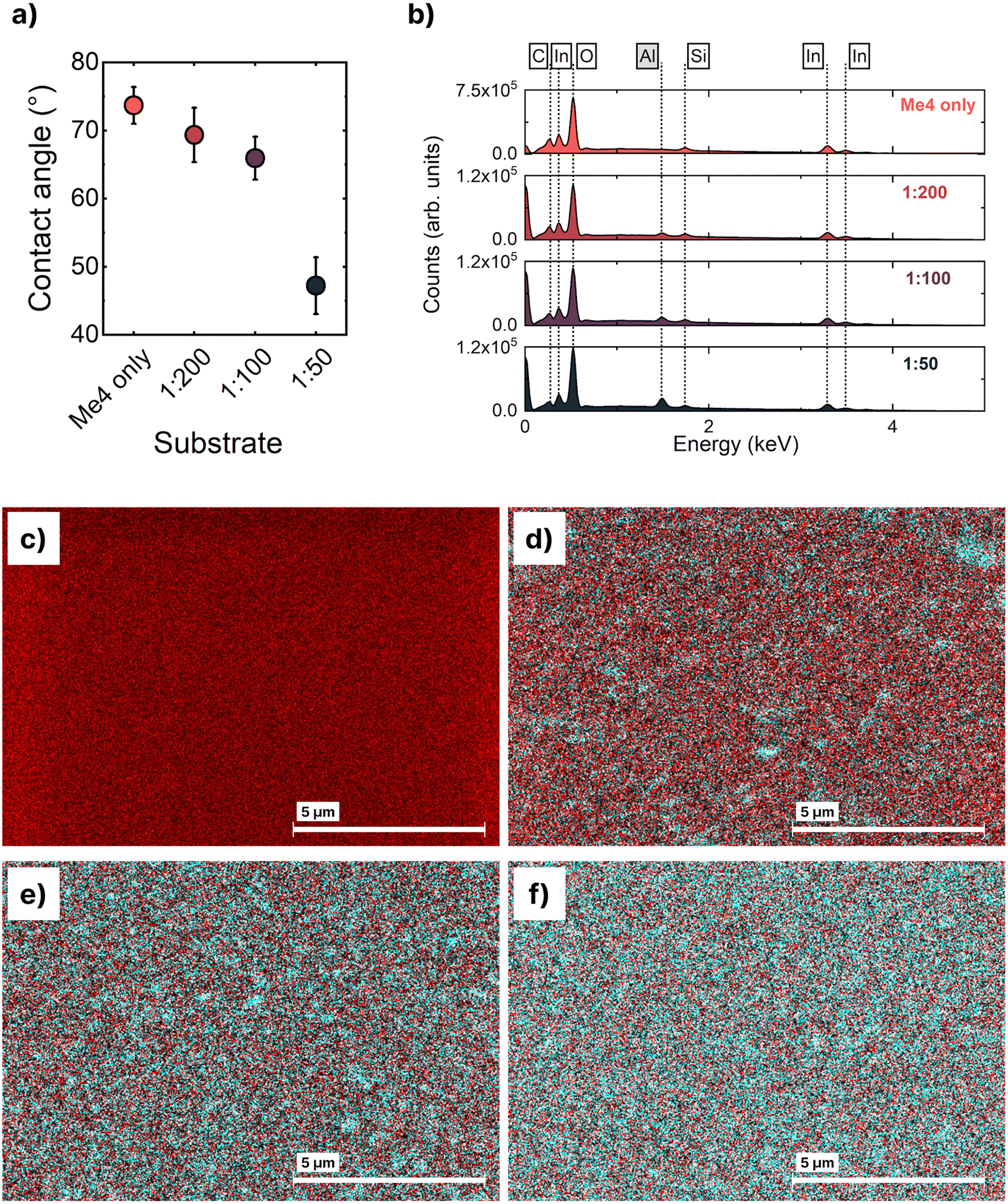 | ||
| Fig. 1 Characterisation of Al2O3 treatment of Me-4PACz thin films on indium tin oxide (ITO) coated glass. (a) Summary of the measured contact angles of a droplet of water on neat Me-4PACz thin films and Al2O3 treated with a range of nanoparticle concentrations. (b) Energy dispersive X-ray (EDX) spectroscopy measurements and corresponding elemental images measured using scanning electron microscopy of thin films of Me-4PACz spin-coated onto indium tin oxide (ITO) glass and treated with Al2O3 nanoparticle solutions diluted with isopropanol in the following ratios (nanoparticles:isopropanol) (c) no nanoparticles, (d) 1:200, (e) 1:100, and (f) 1:50. Red indicates carbon and cyan indicates aluminium. | ||
Subsequently we investigated the effect of increased Al2O3-np concentration on the morphology, crystal structure, and optoelectronic properties of perovskite thin films. A “triple cation” Cs0.05FA0.81MA0.14PbI2.55Br0.45 perovskite thin film was deposited onto Me-4PACz/Al2O3-np coated ITO glass substrates by either spin-coating or ultrasonic spray-coating. As with spin-coating it was not possible to fabricate uniform perovskite thin films using spray-coated on Me-4PACz without Al2O3-nps due to severe dewetting of the perovskite precursor solution. Hereafter, perovskite thin films which are fabricated through spray-coating on either a 1:100 or 1:50 dilution of Al2O3-nps are referred to as “spray 1:100” or “spray 1:50”, respectively. Spray-coating of perovskite thin films atop the 1:200 dilution of nanoparticles resulted in incomplete film formation due to an insufficient modification of the surface energy of the Me-4PACz thin film (Fig. S2, ESI†) and were not further investigated. We compare the properties of our spray-coated perovskite thin films with optimised spin-coated perovskite thin films with a 1:100 dilution of Al2O3-nps on Me-4PACz, these are referred to as “spin 1:100”.
Fig. 2a–c and Fig. S3 (ESI†) show atomic force microscopy (AFM) images of Cs0.05FA0.81MA0.14PbI2.55Br0.45 thin films deposited on to Al2O3 treated Me-4PACz thin films. The corresponding trend in root-mean-squared (RMS) roughness (Rq) is shown in Fig. 2d with full data reported in Table S4 (ESI†). Whilst the perovskite grain size remains relatively consistent we observe a considerable increase in the surface roughness between the spin- and spray-coated thin films and also with increasing concentration of nanoparticles. Whilst the spin-coated thin films are annealed immediately following film deposition our spray-coated films undergo an intermediate vacuum annealing step prior to thermal annealing. Previous reports have shown that the inclusion of DMSO as a co-solvent in perovskite processing onto hydrophobic surfaces can result in dewetting of the thin films during annealing and an increase in the surface roughness of the resulting perovskite thin films.22 The combination of solvent system, the higher vapour pressure of DMF (relative to DMSO), and the vacuum annealing processing step is likely to result in a thin film which has a higher proportion of DMSO present when undergoing the thermal annealing process. This could therefore lead to an increase in film roughness due to the perovskite thin film dewetting from the SAMs. Furthermore, in the spray-coated 1:50 films there are regions that are substantially higher relative to the rest of the film (Fig. S4, ESI†). The EDX data suggests a non-uniform distribution of the nanoparticles and we propose these higher regions are the result of the perovskite film forming atop regions of these clustered nanoparticles. The film thicknesses were measured using a profilometer (Fig. S5 and Table S5, ESI†) and the spray-coated films were observed to be significantly thinner than those fabricated through spin-coating ∼540 nm (spray 1:100) and ∼590 nm (spray 1:50) vs. 670 nm (spin 1:100). Fig. 2e shows X-ray diffraction patterns corresponding to the perovskite thin films on Al2O3 treated Me-4PACz. Additional plots can be found in Fig. S6 and S7 (ESI†). There is a consistent shift in peak positions between the spin and spray-coated samples with the spray-coated samples both exhibiting a shift of 2θ = ∼0.05° towards lower angles. This is typically indicative of an increase in the unit cell size suggesting that there is a structural difference between the spin- and spray-coated films. We note a small peak at ∼12.7° within the spray 1:50 sample, indicative of PbI2 developing during film formation.43
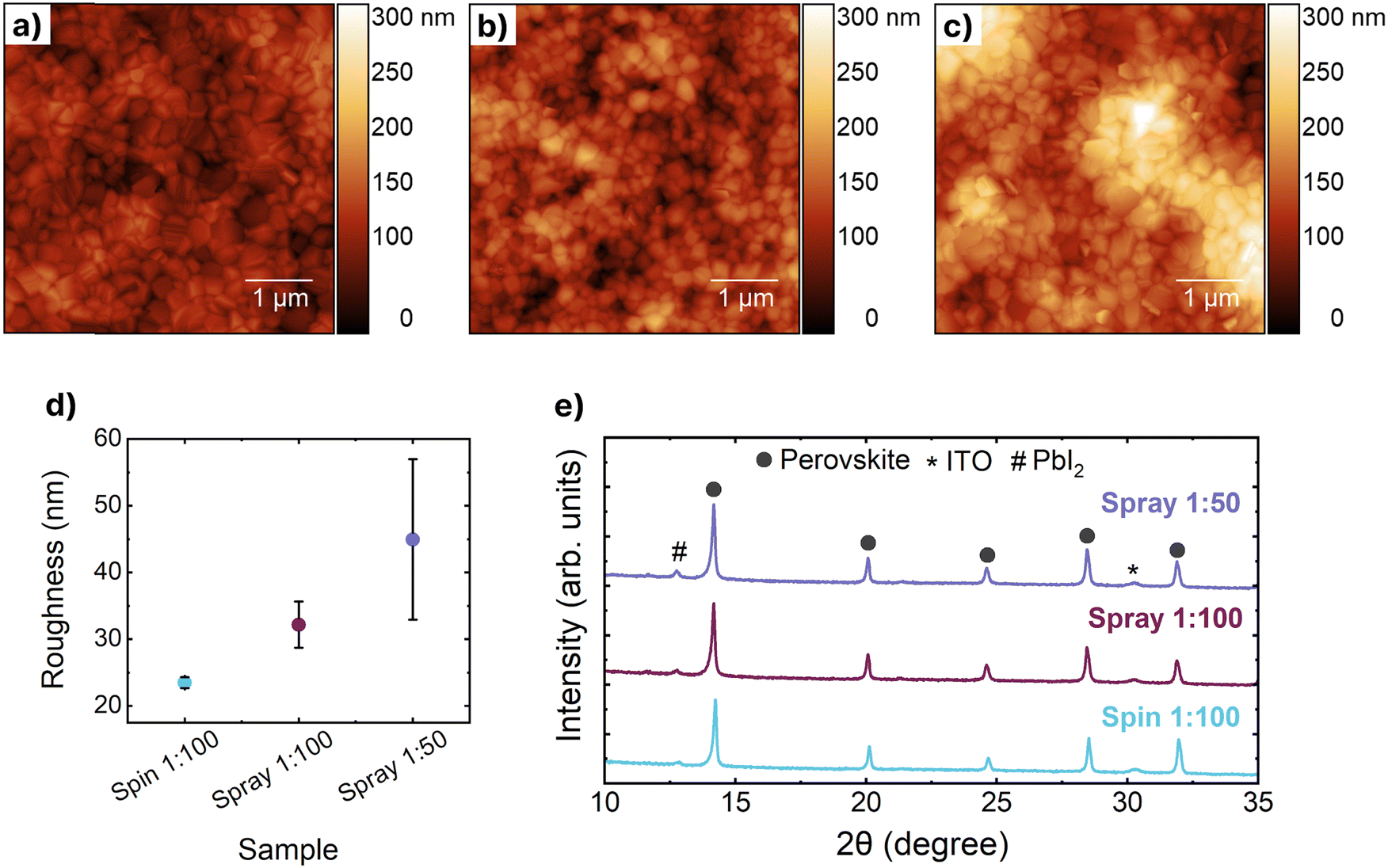 | ||
| Fig. 2 Atomic force microscopy (AFM) images of Cs0.05FA0.81MA0.14PbI2.55Br0.45 thin films on Al2O3 treated Me-4PACz on indium tin oxide (ITO) glass. The perovskite thin films were fabricated through spin- or spray-coating and the ratios represent dilution of nanoparticles:isopropanol. (a) 1:100 spin-coating (b) 1:100 spray-coating and (c) 1:50 spray-coating. (d) root-mean-squared roughness determined from AFM images, error bars represent the mean standard deviation (n = 5) (e) and corresponding X-ray diffraction patterns. | ||
To investigate the influence of this structural change on the optoelectronic properties of these thin films, we conducted photoluminescence (PL) spectroscopy as a function of illumination intensity. As can be seen in Fig. 3a, the centre of the PL peak redshifts substantially between the spin-coated and spray-coated samples for the same Al2O3 concentration. This indicates that the emission is originating from a different structural phase in each sample, suggesting that the different film fabrication routes and subsequent film-formation mechanisms have a strong influence on the optical properties. The magnitude of the red-shift is reduced for the spray-coated 1:50 sample, suggesting that the resulting thin film is more similar to the spin-coated counterpart. Furthermore, the spray-coated samples exhibit an asymmetric PL peak shape. This asymmetry in combination with the red-shifting of the peaks is suggestive of emission from iodide-rich structures44 which is consistent with the peak shifting also observed in the X-ray diffraction measurements. This is further evidence that the metal halide perovskite thin films are not uniform, despite the advances made through the alumina interlayer.
 | ||
| Fig. 3 Optoelectronic properties of Cs0.05FA0.81MA0.14PbI2.55Br0.45 thin films on Al2O3 treated Me-4PACz on indium tin oxide (ITO) glass. Ratios represent dilution of nanoparticles:isopropanol. (a) Intensity dependent steady-state photoluminescence spectra, the integrated area under the peak was then used to calculate (b) the ideality factor, and (c) the absorption coefficient as determined through ultraviolet-visible spectroscopy measurements. The shaded area represents the uncertainty in these measurements. | ||
Fig. 3a also shows a substantial increase in the PL intensity when moving to spray-coated thin films, and with an increased Al2O3 concentration. This is strong evidence for a reduction in the severity of interfacial recombination in these systems. To understand whether the recombination behaviour was changing in these systems, we performed emission measurements across a wide excitation power range which we present in Fig. 3a and summarise in Fig. 3b. The absolute intensity of the peaks is increased by a factor of ∼2.5 and ∼3.5 for spray 1:100 and spray 1:50 over spin 1:100 respectively. However, this increase is not dependent on illumination intensity, giving rise to near identical ideality factors for these systems. This indicates that the underlying recombination mechanisms are unchanged in these systems.
The absorption coefficient of the perovskite thin films was characterised using UV-vis spectroscopy which we show in Fig. 3c. Broadly, the absorption coefficient is similar for each sample with only minor differences. These differences include an apparent increase in below bandgap absorption in the spray-coated samples. However, this is likely due to the spray-coated samples exhibiting an increased roughness (Fig. 2d) resulting in increased scattering.
The absorption onset remains unchanged for each sample, which demonstrates that the bulk perovskite is comparable for each condition. This suggests that the red-shifting of the PL peaks is not a ‘bulk’ effect, but instead originates from a volume of the film that is too small to be detected in absorption measurements. This is likely due to differences in the growth mechanism between the different thin film fabrication routes and due to the differences in the Al2O3 surface modification. This is supported by the clear surface roughness differences between the different systems, determined by AFM measurements, which suggest differences in film formation.
Photovoltaic device performance
To corroborate our structural, morphological and optoelectronic investigations, we fabricated a series of p–i–n photovoltaic devices. All devices had the configuration: ITO-coated glass/Me-4PACz/Al2O3-nps/Cs0.05FA0.81MA0.14PbI2.55Br0.45/C60/bathocuproine (BCP)/Ag, where the perovskite deposition technique and/or Al2O3-nps concentration was altered. We show a statistical summary of the power conversion efficiency (PCE), short-circuit current density (JSC), open-circuit voltage (VOC), and fill factor (FF) in Fig. 4a–d respectively for the different conditions investigated in this study. Additionally, we summarise the device performance statistics in Table 1.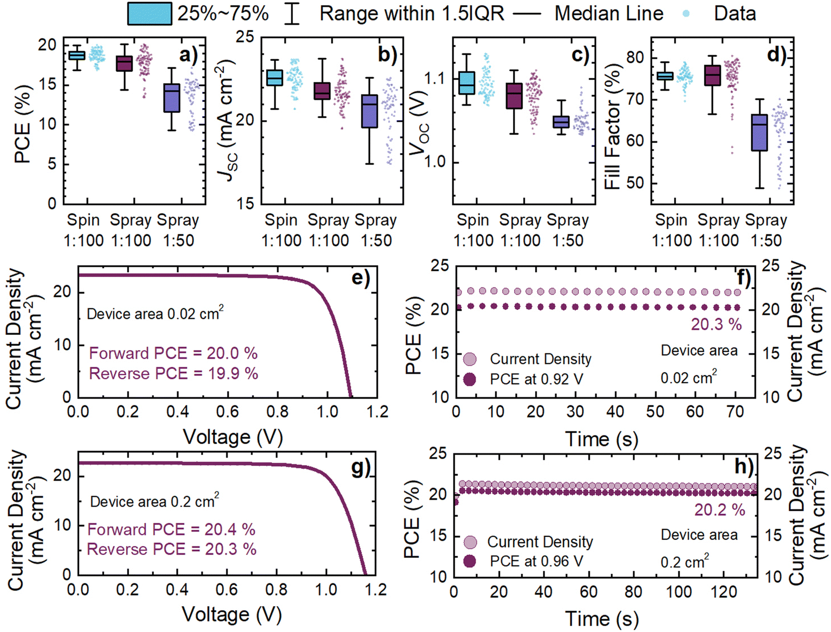 | ||
| Fig. 4 Photovoltaic device performances for p–i–n Cs0.05FA0.81MA0.14PbI2.55Br0.45 devices incorporating optimised Al2O3 nanoparticle interlayer. Box plots for device parameters showing data points relating to (a) power conversion efficiency (PCE), (b) short circuit current density (JSC), (c) open-circuit voltage (VOC), and (d) fill factor. Data relating to champion device performances is shown in (e) JV characteristics for spray (1:100) condition for 0.02 cm2 device active area and (f) corresponding stabilised power conversion efficiency at maximum power point, (g) JV characteristics for spray (1:100) condition for 0.2 cm2 device active area and (f) corresponding stabilised power conversion efficiency at maximum power point. | ||
| J SC (mA cm−2) | V OC (V) | FF (%) | PCE (%) | n devices | |
|---|---|---|---|---|---|
| Spin 1:100 0.025 cm2 |
22.5 ± 0.7 (23.7) | 1.10 ± 0.02 (1.13) | 75.6 ± 1.7 (79.1) | 18.7 ± 0.7 (20.0) | 48 |
| Spray 1:100 0.025 cm2 |
21.8 ± 0.9 (23.7) | 1.08 ± 0.02 (1.11) | 75.4 ± 4.1 (80.6) | 17.7 ± 1.5 (20.1) | 48 |
| Spray 1:50 0.025 cm2 |
20.5 ± 1.5 (22.6) | 1.05 ± 0.01 (1.09) | 62.1 ± 5.7 (70.2) | 13.5 ± 2.2 (17.2) | 32 |
| Spray 1:100 0.2 cm2 |
22.0 ± 1.5 (22.8) | 1.09 ± 0.03 (1.16) | 69.0 ± 5.6 (77.7) | 16.7 ± 2.3 (20.4) | 31 |
The average PCE of spin-coated cells (18.7%, n = 48 devices) is higher than the PCE of spray-coated cells (17.7%, n = 48) for a 1:100 dilution of Al2O3-nps. Whilst the average JSC and VOC of spray 1:100 cells are reduced in comparison to spin 1:100 (22.5 mA cm−2vs. 21.8 mA cm−2, and 1.10 V vs. 1.08 V), device FF remains similar (75.6% vs. 75.4%). The reduction in JSC can be ascribed to the reduced thickness of the spray-coated perovskite. The reduced VOC is surprising, however, since the photoluminescence data in Fig. 3 suggested a reduced degree of non-radiative recombination at the perovskite/SAM interface for spray-coated devices. However, the increased roughness of the spray-coated perovskite has likely impacted the quality of the perovskite/C60 interface, which has resulted in the reduction of the open-circuit voltage. Encouragingly, the maximum device performance of spray 1:100 devices is comparable to the maximum PCE of spin 1:100 cells (20.1% vs. 20.0%, respectively). The current–voltage (JV) curve of the best-performing spray 1:100 device (active area of 0.02 cm2) is shown in Fig. 4e. Fig. S9 and S10 (ESI†) shows the external quantum efficiency (EQE) response for the champion cells of each condition. The integrated short-circuit current density (JSC-EQE) calculated using the EQE data is in good agreement with the JSC extracted from the current–voltage characteristics. For the spray 1:100 device the JSC-EQE = 22.6 mA cm−2 compared to 23.3 mA cm−2 for the measured JSC The mismatch is just 3% providing confidence to our solar simulator measurements. We calculated the photovoltaic bandgap,45–47 shown in Fig. S11 (ESI†), using the derivative of the EQE with respect to energy. This yields a bandgap of 1.62 eV, consistent with the optical data presented in Fig. 3.
The stabilised power output of the champion spray 1:100 device at maximum power point was 20.3% (Fig. 4f) which constitutes a record performance for both spray-coated triple cation and spray-coated p–i–n photovoltaic devices.24,41,48–50 This demonstrates the effectiveness of the Al2O3-np interlayer approach as compared to other techniques. Indeed, our champion device outperforms the spin-coated counterpart (with no additional passivation) Me-4PACz devices in the literature.19,20,26,51–53 This highlights the potential of this approach for demonstrating spray-coated high-performance perovskite photovoltaics enabling high-throughput fabrication. Photovoltaic devices based on the spray 1:50 condition were fabricated, but the improvements implied by the optoelectronic measurements were not present in the device performance. The deterioration in device performance can be attributed to several factors. The increased roughness of the perovskite will lead to increased interfacial recombination limiting the VOC and reducing the shunt resistance (Fig. S12, ESI†). The increased coverage of the insulating Al2O3 interlayer partially inhibits charge transfer to the SAM, which simultaneously constrains the JSC and FF of these devices.
We investigated the ideality factor of photovoltaic devices based on each condition through light intensity dependent JV measurements. Fig. S13(a, c and e) (ESI†) show a double logarithmic plot of JSCversus light intensity and (b, d and e) show the light-dependent VOC response for spray 1:50, spray 1:100, and spin 1:100 cells, respectively. The ideality factor (n) of the devices was found to be 1.46 (spray 1:50), 1.10 (spray 1:100), and 1.13 (spin 1:100) kBT/q respectively. Contrastingly, the ideality factors determined in Fig. 3(b) from perovskite thin-films on Al2O3-np-coated Me-4PACz (without an electron-transporting layer) were near identical for each device type. This change in ideality factor for spray 1:50 devices supports our suggestion that the increased roughness at the C60/perovskite interface in these samples is influencing the recombination processes that are occurring.54 Additionally, this inferior morphology and increased surface recombination would simultaneously constrain the FF, as observed in our devices.
To explore the applicability of our Al2O3-np interlayer for large scale deposition of spray-coated perovskite layers onto Me-4PACz, we fabricated spray-coated devices with larger active areas (0.2 cm2 and 1 cm2) incorporating the best performing interlayer condition (1:100). The champion 0.2 cm2 device demonstrated a stabilised PCE of 20.2% (Fig. 4g and h), equivalent to smaller area devices. Fig. S14 (ESI†) shows histogram plots of the device PCE distribution for each active area of spray 1:100 cells (0.02 cm2 and 0.2 cm2) which shows comparable performance for each condition. All device parameters for these 0.02 cm2 and 0.2 cm2 devices are summarised in Fig. S15 (ESI†). We show champion JV characteristics and stabilised PCE for 1 cm2 devices of both the spin 1:100 and spray 1:100 conditions in Fig. S16 (ESI†). For these conditions we achieve a maximum stabilised PCE of ∼17% for both conditions.
Interestingly, upon scale-up to 0.2 cm2 we observe an increased median JSC and VOC. This indicates a reduced severity of non-radiative recombination in these devices as well as efficient charge-extraction at short-circuit conditions. This suggests an improvement in the formation of the thin film layers resulting in a reduction in structural defects and hence recombination sites. However, the median PCE is reduced slightly, due to an inferior FF for the 0.2 cm2 devices, highlighting a charge transport limitation in these systems. From inspecting the JV curve in Fig. 4g, this reduced FF originates from an increased series resistance within the scaled-up photovoltaics. We attribute this to the sheet resistance of our ITO substrates (∼20 Ω □−1) becoming significant in these larger devices. This phenomenon is exacerbated for 1 cm2 devices where we observe the FF being constrained to ∼66–68%. This arises from the gradient in the JV curves near VOC becoming increasingly shallow, characteristic of an increased series resistance.
Therefore, this limitation is not intrinsic to the Al2O3-np layer we report here, highlighting that with sufficiently low sheet resistance, this approach is applicable for even larger area scale-up.
Conclusions
In summary, we have demonstrated an optimised Al2O3 interlayer which enables scalable, spray-coating of high performance 1.62 eV p–i–n metal halide perovskite photovoltaics onto the Me-4PACz SAM charge transporting layer. We demonstrated that the incorporation of this interlayer between the Me-4PACz and perovskite thin films results in spray-coated perovskite layers with improved structural and optoelectronic properties relative to their spin-coated counterparts. As a result we report champion photovoltaic devices with efficiencies of up to 20.4% which represents the state-of-the-art for spray-coated p–i–n PSCs. The improvements in device performance resulting from the incorporation of the optimised Al2O3-np interlayer remained effective as the device active area was scaled from 0.02 cm2 to 0.2 cm2, suggesting that this approach warrants further investigation for large area photovoltaic devices fabricated through high-throughput solution processing routes.Author contributions
Elena J. Cassella: conceptualization, methodology, investigation, formal analysis, writing – original draft, review and editing. Robert D.J. Oliver: conceptualization, methodology, investigation, formal analysis, supervision, writing – original draft, review and editing. Timothy Thornber: methodology, investigation, formal analysis, writing – original draft, review and editing. Sophie Tucker: investigation, formal analysis. Rehmat Goodwin: investigation, formal analysis. David G. Lidzey: conceptualization, supervision, funding acquisition, writing – review and editing. Alexandra J. Ramadan: conceptualization, methodology, supervision, funding acquisition, writing – original draft, writing – review and editing.Data availability
Data for this article, including raw data and processed data are available at ORDA at https://doi.org/10.15131/shef.data.26180623.Conflicts of interest
D. G. L. is co-chairman of the materials science company Ossila Ltd. which retails materials and equipment for photovoltaic research, including perovskite photovoltaics.Acknowledgements
This work was funded by the Engineering and Physical Sciences Research Council (EPSRC) grants EP/V027131/1, EP/X039285/1 and EP/T012455/1. T. T. acknowledges the Faculty of Science, University of Sheffield for a studentship. S. T. and R. G. acknowledge the EPSRC and the Grantham Centre for Sustainable Futures for funding. R. G. also acknowledges the University of Sheffield's Energy Institute for funding.References
- S. D. Stranks, G. E. Eperon, G. Grancini, C. Menelaou, M. J. P. Alcocer, T. Leijtens, L. M. Herz, A. Petrozza and H. J. Snaith, Science, 2013, 342, 341–344 CrossRef CAS PubMed.
- S. De Wolf, J. Holovsky, S.-J. Moon, P. Löper, B. Niesen, M. Ledinsky, F.-J. Haug, J.-H. Yum and C. Ballif, J. Phys. Chem. Lett., 2014, 5, 1035–1039 CrossRef CAS PubMed.
- A. Miyata, A. Mitioglu, P. Plochocka, O. Portugall, J. T.-W. Wang, S. D. Stranks, H. J. Snaith and R. J. Nicholas, Nat. Phys., 2015, 11, 582–587 Search PubMed.
- C. Wehrenfennig, G. E. Eperon, M. B. Johnston, H. J. Snaith, L. M. Herz, C. Wehrenfennig, G. E. Eperon, M. B. Johnston, H. J. Snaith and L. M. Herz, Adv. Mater., 2014, 26, 1584–1589 CrossRef CAS PubMed.
- Z. Li, T. R. Klein, D. H. Kim, M. Yang, J. J. Berry, M. F. A. M. Van Hest and K. Zhu, Nat. Rev. Mater., 2018, 3, 1–20 CrossRef CAS.
- L. Zhang, L. Mei, K. Wang, Y. Lv, S. Zhang, Y. Lian, X. Liu, Z. Ma, G. Xiao, Q. Liu, S. Zhai, S. Zhang, G. Liu, L. Yuan, B. Guo, Z. Chen, K. Wei, A. Liu, S. Yue, G. Niu, X. Pan, J. Sun, Y. Hua, W.-Q. Wu, D. Di, B. Zhao, J. Tian, Z. Wang, Y. Yang, L. Chu, M. Yuan, H. Zeng, H.-L. Yip, K. Yan, W. Xu, L. Zhu, W. Zhang, G. Xing, F. Gao and L. Ding, Nano-Micro Lett., 2023, 15, 177 CrossRef PubMed.
- Z.-Y. Chen, N.-Y. Huang and Q. Xu, Coord. Chem. Rev., 2023, 481, 215031 CrossRef CAS.
- A. Fakharuddin, M. K. Gangishetty, M. Abdi-Jalebi, S.-H. Chin, A. R. bin Mohd Yusoff, D. N. Congreve, W. Tress, F. Deschler, M. Vasilopoulou and H. J. Bolink, Nat. Electron., 2022, 5, 203–216 CrossRef CAS.
- Y. Wu, J. Feng, Z. Yang, Y. Liu and S. (Frank) Liu, Adv. Sci., 2023, 10, 2205536 CrossRef CAS PubMed.
- N. Rolston, W. J. Scheideler, A. C. Flick, J. P. Chen, H. Elmaraghi, A. Sleugh, O. Zhao, M. Woodhouse and R. H. Dauskardt, Joule, 2020, 4, 2675–2692 CrossRef CAS.
- L.-H. Chou, J. M. W. Chan and C.-L. Liu, Sol. RRL, 2022, 6, 2101035 CrossRef CAS.
- W. Tress, Adv. Energy Mater., 2017, 7, 1602358 CrossRef.
- C. M. Wolff, P. Caprioglio, M. Stolterfoht and D. Neher, Adv. Mater., 2019, 31, 1902762 CrossRef CAS PubMed.
- M. Stolterfoht, P. Caprioglio, C. M. Wolff, J. A. Márquez, J. Nordmann, S. Zhang, D. Rothhardt, U. Hörmann, Y. Amir, A. Redinger, L. Kegelmann, F. Zu, S. Albrecht, N. Koch, T. Kirchartz, M. Saliba, T. Unold and D. Neher, Energy Environ. Sci., 2019, 12, 2778–2788 RSC.
- A. Al-Ashouri, A. Magomedov, M. Roß, M. Jošt, M. Talaikis, G. Chistiakova, T. Bertram, J. A. Márquez, E. Köhnen, E. Kasparavičius, S. Levcenco, L. Gil-Escrig, C. J. Hages, R. Schlatmann, B. Rech, T. Malinauskas, T. Unold, C. A. Kaufmann, L. Korte, G. Niaura, V. Getautis and S. Albrecht, Energy Environ. Sci., 2019, 12, 3356–3369 RSC.
- A. Magomedov, A. Al-Ashouri, E. Kasparavičius, S. Strazdaite, G. Niaura, M. Jošt, T. Malinauskas, S. Albrecht and V. Getautis, Adv. Energy Mater., 2018, 8, 1801892 CrossRef.
- A. Al-Ashouri, E. Köhnen, B. Li, A. Magomedov, H. Hempel, P. Caprioglio, J. A. Márquez, A. B. Morales Vilches, E. Kasparavicius, J. A. Smith, N. Phung, D. Menzel, M. Grischek, L. Kegelmann, D. Skroblin, C. Gollwitzer, T. Malinauskas, M. Jošt, G. Matič, B. Rech, R. Schlatmann, M. Topič, L. Korte, A. Abate, B. Stannowski, D. Neher, M. Stolterfoht, T. Unold, V. Getautis and S. Albrecht, Science, 2020, 370, 1300–1309 CrossRef CAS PubMed.
- M. Roß, S. Severin, M. B. Stutz, P. Wagner, H. Köbler, M. Favin-Lévêque, A. Al-Ashouri, P. Korb, P. Tockhorn, A. Abate, B. Stannowski, B. Rech and S. Albrecht, Adv. Energy Mater., 2021, 11, 2101460 CrossRef.
- A. Kulkarni, R. Sarkar, S. Akel, M. Häser, B. Klingebiel, M. Wuttig, S. Wiegand, S. Chakraborty, M. Saliba and T. Kirchartz, Adv. Funct. Mater., 2023, 33, 2305812 CrossRef CAS.
- A. Al-Ashouri, M. Marčinskas, E. Kasparavičius, T. Malinauskas, A. Palmstrom, V. Getautis, S. Albrecht, M. D. McGehee and A. Magomedov, ACS Energy Lett., 2023, 8, 898–900 CrossRef CAS.
- F. H. Isikgor, A. S. Subbiah, M. K. Eswaran, C. T. Howells, A. Babayigit, M. De Bastiani, E. Yengel, J. Liu, F. Furlan, G. T. Harrison, S. Zhumagali, J. I. Khan, F. Laquai, T. D. Anthopoulos, I. McCulloch, U. Schwingenschlögl and S. De Wolf, Nano Energy, 2021, 81, 105633 CrossRef CAS.
- K. O. Brinkmann, J. He, F. Schubert, J. Malerczyk, C. Kreusel, F. van gen Hassend, S. Weber, J. Song, J. Qu and T. Riedl, ACS Appl. Mater. Interfaces, 2019, 11, 40172–40179 CrossRef CAS PubMed.
- J. Li, J. Dagar, O. Shargaieva, M. A. Flatken, H. Köbler, M. Fenske, C. Schultz, B. Stegemann, J. Just, D. M. Többens, A. Abate, R. Munir and E. Unger, Adv. Energy Mater., 2021, 11, 2003460 CrossRef CAS.
- E. J. Cassella, E. L. K. Spooner, T. Thornber, M. E. O’Kane, T. E. Catley, J. E. Bishop, J. A. Smith, O. S. Game and D. G. Lidzey, Adv. Sci., 2022, 9, 2104848 CrossRef CAS PubMed.
- Q. Cao, T. Wang, X. Pu, X. He, M. Xiao, H. Chen, L. Zhuang, Q. Wei, H.-L. Loi, P. Guo, B. Kang, G. Feng, J. Zhuang, G. Feng, X. Li and F. Yan, Adv. Mater., 2024, 36(16), 2311970 CrossRef CAS PubMed.
- K. Hossain, A. Kulkarni, U. Bothra, B. Klingebiel, T. Kirchartz, M. Saliba and D. Kabra, ACS Energy Lett., 2023, 8, 3860–3867 CrossRef CAS.
- X. Zheng, Z. Li, Y. Zhang, M. Chen, T. Liu, C. Xiao, D. Gao, J. B. Patel, D. Kuciauskas, A. Magomedov, R. A. Scheidt, X. Wang, S. P. Harvey, Z. Dai, C. Zhang, D. Morales, H. Pruett, B. M. Wieliczka, A. R. Kirmani, N. P. Padture, K. R. Graham, Y. Yan, M. K. Nazeeruddin, M. D. McGehee, Z. Zhu and J. M. Luther, Nat. Energy, 2023, 8, 462–472 CrossRef CAS.
- A. Farag, T. Feeney, I. M. Hossain, F. Schackmar, P. Fassl, K. Küster, R. Bäuerle, M. A. Ruiz-Preciado, M. Hentschel, D. B. Ritzer, A. Diercks, Y. Li, B. A. Nejand, F. Laufer, R. Singh, U. Starke and U. W. Paetzold, Adv. Energy Mater., 2023, 13, 2203982 CrossRef CAS.
- M. Pitaro, J. E. S. Alonso, L. Di Mario, D. G. Romero, K. Tran, J. Kardula, T. Zaharia, M. B. Johansson, E. M. J. Johansson, R. C. Chiechi and M. A. Loi, Adv. Funct. Mater., 2023, 2306571 CrossRef.
- Y. Xu, F. Fei, X. Dong, L. Li, Y. Li, N. Yuan and J. Ding, Sol. RRL, 2023, 7, 2300283 CrossRef CAS.
- N. Phung, M. Verheijen, A. Todinova, K. Datta, M. Verhage, A. Al-Ashouri, H. Köbler, X. Li, A. Abate, S. Albrecht and M. Creatore, ACS Appl. Mater. Interfaces, 2022, 14, 2166–2176 CrossRef CAS PubMed.
- D. Takhellambam, L. A. Castriotta, G. Zanotti, L. Mancini, V. Raglione, G. Mattioli, B. Paci, A. Generosi, M. Guaragno, V. Campanari, G. Ammirati, F. Martelli, E. Calabrò, A. Cricenti, M. Luce, N. Yaghoobi Nia, F. Di Giacomo and A. Di Carlo, Sol. RRL, 2023, 7, 2300658 CrossRef CAS.
- S.-C. Liu, H.-Y. Lin, S.-E. Hsu, D.-T. Wu, S. Sathasivam, M. Daboczi, H.-J. Hsieh, C.-S. Zeng, T.-G. Hsu, S. Eslava, T. J. Macdonald and C.-T. Lin, J. Mater. Chem. A, 2024, 12, 2856–2866 RSC.
- M. Taddei, J. A. Smith, B. M. Gallant, S. Zhou, R. J. E. Westbrook, Y. Shi, J. Wang, J. N. Drysdale, D. P. McCarthy, S. Barlow, S. R. Marder, H. J. Snaith and D. S. Ginger, ACS Energy Lett., 2022, 7, 4265–4273 CrossRef CAS.
- W. Peng, K. Mao, F. Cai, H. Meng, Z. Zhu, T. Li, S. Yuan, Z. Xu, X. Feng, J. Xu, M. D. McGehee and J. Xu, Science, 2023, 379, 683–690 CrossRef CAS PubMed.
- W. H. K. Perera, M. G. Masteghin, H. Shim, J. D. Davies, J. L. Ryan, S. J. Hinder, J. S. Yun, W. Zhang, K. D. G. I. Jayawardena and S. R. P. Silva, Sol. RRL, 2023, 2300388, 1–11 Search PubMed.
- Y. Diao, L. Shaw, Z. Bao and S. C. B. Mannsfeld, Energy Environ. Sci., 2014, 7, 2145–2159 RSC.
- J. E. Bishop, J. A. Smith and D. G. Lidzey, ACS Appl. Mater. Interfaces, 2020, 12, 48237–48245 CrossRef CAS PubMed.
- T. Carey, C. Jones, F. Le Moal, D. Deganello and F. Torrisi, ACS Appl. Mater. Interfaces, 2018, 10, 19948–19956 CrossRef CAS PubMed.
- T. Thornber, O. S. Game, E. J. Cassella, M. E. O’Kane, J. E. Bishop, T. J. Routledge, T. I. Alanazi, M. Togay, P. J. M. Isherwood, L. C. Infante-Ortega, D. B. Hammond, J. M. Walls and D. G. Lidzey, ACS Appl. Mater. Interfaces, 2022, 14, 37587–37594 CrossRef CAS PubMed.
- J. E. Bishop, C. D. Read, J. A. Smith, T. J. Routledge and D. G. Lidzey, Sci. Rep., 2020, 10, 6610 CrossRef CAS PubMed.
- D. Nečas and P. Klapetek, Open Phys., 2012, 10, 181–188 CrossRef.
- T. J. Jacobsson, J.-P. Correa-Baena, E. Halvani Anaraki, B. Philippe, S. D. Stranks, M. E. F. Bouduban, W. Tress, K. Schenk, J. Teuscher, J.-E. Moser, H. Rensmo and A. Hagfeldt, J. Am. Chem. Soc., 2016, 138, 10331–10343 CrossRef CAS PubMed.
- A. J. Knight, J. Borchert, R. D. J. Oliver, J. B. Patel, P. G. Radaelli, H. J. Snaith, M. B. Johnston and L. M. Herz, ACS Energy Lett., 2021, 6, 799–808 CrossRef CAS PubMed.
- P. K. Nayak, S. Mahesh, H. J. Snaith and D. Cahen, Nat. Rev. Mater., 2019, 4, 269–285 CrossRef CAS.
- U. Rau, B. Blank, T. C. M. Müller and T. Kirchartz, Phys. Rev. Appl., 2017, 7, 044016 CrossRef.
- A. J. Ramadan, R. D. J. Oliver, M. B. Johnston and H. J. Snaith, Nat. Rev. Mater., 2023, 8, 822–838 CrossRef CAS.
- J. Su, H. Cai, J. Yang, X. Ye, R. Han, J. Ni, J. Li and J. Zhang, ACS Appl. Mater. Interfaces, 2019, 12, 3531–3538 CrossRef PubMed.
- J. E. Bishop, J. A. Smith, C. Greenland, V. Kumar, N. Vaenas, O. S. Game, T. J. Routledge, M. Wong-Stringer, C. Rodenburg and D. G. Lidzey, ACS Appl. Mater. Interfaces, 2018, 10, 39428–39434 CrossRef CAS PubMed.
- M. Park, S. C. Hong, Y. W. Jang, J. Byeon, J. Jang, M. Han, U. Kim, K. Jeong, M. Choi and G. Lee, Int. J. Precis. Eng. Manuf., 2022, 1–12 Search PubMed.
- J. Siekmann, A. Kulkarni, S. Akel, B. Klingebiel, M. Saliba, U. Rau and T. Kirchartz, Adv. Energy Mater., 2023, 13, 2300448 CrossRef CAS.
- Y. Yuan, G. Yan, C. Dreessen, T. Rudolph, M. Hülsbeck, B. Klingebiel, J. Ye, U. Rau and T. Kirchartz, Nat. Mater., 2024, 23, 391–397 CrossRef CAS PubMed.
- Y. Wang, S. Akel, B. Klingebiel and T. Kirchartz, Adv. Energy Mater., 2024, 14, 2302614 CrossRef CAS.
- P. Caprioglio, C. M. Wolff, O. J. Sandberg, A. Armin, B. Rech, S. Albrecht, D. Neher and M. Stolterfoht, Adv. Energy Mater., 2020, 10, 2000502 CrossRef CAS.
Footnotes |
| † Electronic supplementary information (ESI) available. See DOI: https://doi.org/10.1039/d4tc01602e |
| ‡ These authors contributed equally. |
| This journal is © The Royal Society of Chemistry 2024 |