 Open Access Article
Helical interfacial modulation for perovskite photovoltaics†
Ghewa
AlSabeh‡
 ab,
Masaud
Almalki‡
 a,
Sitthichok
Kasemthaveechok‡
 c,
Marco A.
Ruiz-Preciado
a,
Hong
Zhang§
a,
Nicolas
Vanthuyne
 dg,
Paul
Zimmermann
e,
Daphne M.
Dekker
f,
Felix Thomas
Eickemeyer
a,
Alexander
Hinderhofer
e,
Frank
Schreiber
 e,
Shaik M.
Zakeeruddin
a,
Bruno
Ehrler
 f,
Jeanne
Crassous
 *c,
Jovana V.
Milić
 *ab and
Michael
Grätzel
*a
aLaboratory of Photonics and Interfaces, Institute of Chemical Sciences and Engineering, École Polytechnique Fédérale de Lausanne, Lausanne, Switzerland. E-mail: michael.graetzel@epfl.ch
bAdolphe Merkle Institute, University of Fribourg, Fribourg, Switzerland. E-mail: jovana.milic@unifr.ch
cUniv. Rennes, CNRS, ISCR – UMR 6226, Rennes, France. E-mail: jeanne.crassous@univ-rennes1.fr
dAix Marseille University, CNRS Centrale Marseille, iSm2, Marseille, France
eInstitute of Applied Physics, University of Tübingen, 72076 Tübingen, Germany
fAMOLF, Science Park 104, Amsterdam, The Netherlands
gAix-Marseille University, CNRS, Centrale Marseille, FSCM, Chiropole, Marseille, France
First published on 30th May 2024
Abstract
Hybrid metal halide perovskites have demonstrated remarkable performances in modern photovoltaics, although their stabilities remain limited. We assess the capacity to advance their properties by relying on interfacial modulators featuring helical chirality based on P,M-(1-methylene-3-methyl-imidazolium)[6]helicene iodides. We investigate their characteristics, demonstrating comparable charge injection for enantiomers and the racemic mixture. Overall, they maintain the resulting photovoltaic performance while improving operational stability, challenging the role of helical chirality in the interfacial modulation of perovskite solar cells.
Hybrid halide perovskites have gradually increased their solar-to-electric power conversion efficiencies in photovoltaics over the past decade.1 They, however, feature limited stability under device operating conditions,2–4 which are especially pronounced at the interface with the selective charge-transport layers.4–7 In the case of hole-transporting materials (HTMs), such as the commonly employed 2,2′,7,7′-tetrakis[N,N-di(4-methoxyphenyl)amino]-9,9′-spirobifluorene (spiro-OMeTAD), ion-migration-induced processes are pronounced due to the use of doping agents based on metal salts, which can migrate into the perovskite layer and be detrimental for their performances.4–7 To suppress the degradation processes, a common strategy refers to using interlayers between the perovskite and charge-transport layers, such as in the form of molecular assemblies or graphene composites.2,4,8–11 However, these layers could interfere with hole injection, and it is of interest to employ alternative assemblies that do not interfere with the charge transport. There has recently been a development of several helically chiral systems that were shown to facilitate electron transport through chiral-induced spin selectivity (CISS) phenomena using chiral molecular systems,12–15 in particular those featuring helical chirality.14–16 This can facilitate electron transfer through chiral molecular assemblies.14,15,17 Chiral moieties have already demonstrated promise in hybrid perovskite optoelectronics18–28 and chiral perovskites were presented as promising materials for next-generation optoelectronics due to electronic circular dichroism,24 non-linear optical activity,25 and circularly polarized emission.26 For instance, it was shown that α-methylbenzylammonium (MBA) based (R/S-MBA)2PbI4 films display CISS effect.19 Moreover, a spin-LED has recently showed effective circularly polarized electroluminescence at room temperature using CsPbI3 heterostructures with (R/S-MBA)2PbI4 overlayers.27 However, their utility in selective charge transfer for hybrid perovskite photovoltaics remains underexploited.22,24
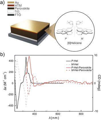
Here, we assess the use of chiral molecular assemblies based on functional [6]helicenes, namely P,M-(1-methylene-3-methyl-imidazolium)[6]helicene iodides, in conventional n-i-p perovskite solar cells (Fig. 1a). Helicene assemblies have demonstrated the CISS effect,28–30 and introducing suitable anchoring groups31–34 enables functionalizing the hybrid halide perovskite interface.35–37 We have assembled functionalized [6]helicene moieties38,39 at the interface with the hole-transport layers. This resulted in comparable photovoltaic performances of hybrid perovskite solar cells, which were accompanied by enhanced operational stabilities, thus challenging the role of helical interfacial modulation in hybrid perovskite photovoltaics.
 | ||
| Fig. 1 (a) Schematic of the perovskite solar cell and the corresponding layers. The interfacial modulation is applied between the perovskite (brown) and hole-transporting layers (HTM, red). Inset shows the M- and P-2-(1-methylene-3-methyl-imidazolium)[6]helicene iodide structures (abbreviated as M- and P-Hel). The synthesis and characterization are detailed in the ESI (Fig. S1–S14 and Tables S1–S5†). (b) ECD spectra of P-Hel (black) and M-Hel (dashed grey) and perovskite films with P-Hel (solid red) and P-Hel (dashed red), evidencing chiral modulation at the hybrid perovskite interface. | ||
Hybrid perovskite films based on conventional double-cation (FA0.95MA0.05Pb(I0.95Br0.05)3) and triple-cation halide perovskite ((FA0.9MA0.1)0.95Cs0.05Pb1.03(I0.93Br0.1)3) compositions were deposited on glass substrates via previously reported procedures detailed in the Experimental section (ESI†).35–37 The modulation was performed at the interface with the HTM from a tetrachloroethane solution in the concentrations of 0.5–1 mg mL−1, followed by annealing for 10 min at 100 °C. The formation of the chiral assemblies was evidenced using electronic circular dichroism (ECD) spectroscopy (Fig. 1b).23
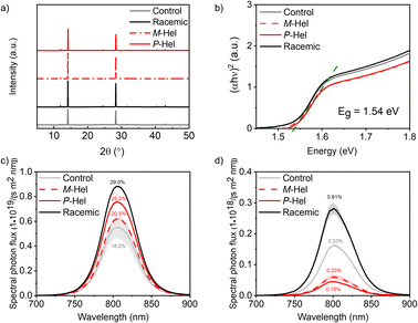
Structural properties were investigated by X-ray diffraction (XRD; Fig. 2a). XRD patterns of the modulated perovskite films closely matched those of the control perovskites, suggesting comparable characteristics across material compositions (Fig. S15, ESI†). This was in accordance with the grazing incidence wide-angle X-ray scattering (GIWAXS) measurements (Fig. S16†). The control sample displayed a preferred orientation towards 35° and 65° with respect to the substrate, which remained the same upon modulation with M-Hel, whereas using either P-Hel or racemic mixture resulted in a minor change in the orientation with a broader distribution. All samples showed a perovskite phase with a certain amount of residual PbI2, indicated by a signal at q = 0.9 A−1. The control sample also showed the presence of the hexagonal δ-FAPbI3 phase, which was present in a much smaller amount for the modulated samples, likely due to the stabilization of the perovskite phase. This was especially the case for the P-Hel samples, which revealed two additional peaks at 0.659° A−1 and 0.696° A−1, associated with a low-dimensional phase incorporating the solvent molecules, similar to (MA)2Pb3I8 × 2DMSO. In contrast, M-Hel and racemic mixture modulation did not show additional phases. The films were further assessed by infrared (IR) spectroscopy (Fig. S17a†), confirming that the structural integrity was preserved, whereas the analysis of the film morphology by scanning electron microscopy (SEM) suggested minor improvement in homogeneity for the racemic modulation (Fig. S18†). Furthermore, X-ray photoelectron spectroscopy (XPS; Fig. S17b†) revealed Pb 4f7/2 and 4f5/2 signals at 138.77 and 143.66 eV, respectively, with the control films featuring additional peaks at 136.98 and 141.83 eV that correspond to the metallic lead. These peaks were not apparent in modulated samples, suggesting that helical modulators might suppress their formation, likely through the surface interaction with Pb(II) that can affect optoelectronic characteristics.
 | ||
| Fig. 2 Effect of helical modulation on the properties of FA0.97MA0.03Pb(I0.97Br0.03)3 perovskite films. (a) XRD patterns and (b) the corresponding Tauc plots. (c and d) Absolute intensity steady-state PL for control (grey) and modulated (red, black) films on microscope glass in the absence (c) and presence (d) of HTM (spiro-OMeTAD). Numbers represent PLQY and quasi-Fermi level splitting (ΔEF; Table S6†).40 TRPL data is shown in Fig. S19–S21.† | ||
The optoelectronic properties of the films were analysed by steady-state UV-Vis absorption and photoluminescence (PL) spectroscopy (Fig. 2b–d). UV-Vis spectra (Fig. 2b) revealed a comparable optical bandgap of about 1.54–1.56 eV for the helically modulated perovskite and the control samples, in accordance with the preservation of the perovskite structure. PL measurements (Fig. 2c) of modulated double cation perovskite films on glass showed an enhanced PL quantum yield (PLQY) compared to the control films, which is an indication of surface defect passivation. For triple-cation perovskites, we did not observe a beneficial effect on defect passivation by helicene-modulation (Fig. S15†) suggesting that the effect depends on the perovskite composition. Upon the addition of spiro-OMeTAD, the PLQY was decreased by more than one order of magnitude for all samples. In the control films without any modulator, this was expected due to the introduction of defect states by the PbI2-complexing additives in the HTM layer (e.g., 4-tert-butylpyridine).40 However, for the modulated films, we observed a PLQY decrease for the M- and P-Hel, and a PLQY increase with the racemic mixture (Fig. 2d), pointing at a more efficient protection of the perovskite surface by the racemic mixture as compared to the enantiomers, which was expected to affect their photovoltaic properties.
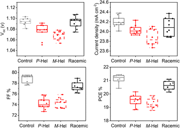
The photovoltaic characteristics were assessed in conventional n-i-p device architectures based on the fluorine-doped tin oxide (FTO)/compact (c) TiO2 (∼60 nm)/mesoporous (mp) TiO2 (∼100 nm)/perovskite (∼575 nm)/HTM (∼200 nm)/Au (∼80 nm) (Fig. 1a and S18†) with two perovskite compositions (detailed in the Experimental section of the ESI and figure captions†). The layer thicknesses were assessed by cross-sectional scanning electron microscopy (SEM; Fig. S18†). M- and P-Hel modulated samples showed (Fig. 3) a reduced power conversion efficiency (PCE) mainly due to lower open-circuit voltage (VOC) and fill factor (FF). The reduced VOC was in accordance with the lower quasi-Fermi level splitting (ΔEF) deduced from PLQY (Fig. 2c and Table S6†). The racemic mixture showed a higher VOC compared to the enantiomers, which is in good agreement with the ΔEF trend. A similar VOC of the racemic mixture as the control (Fig. 3), despite higher ΔEF, arose from the effect of the added interfaces in the devices as compared to films (Fig. 2d). The improved photovoltaic characteristics for the racemic mixture as compared to the enantiopure samples further corroborated that helical chirality through either heterochiral racemic (P/M) or homochiral enantiopure (M/M or P,P) assemblies had a different impact on the performance under these experimental conditions. Moreover, the devices based on alternative perovskite layers showed a higher performance upon modulation with the enantiomers as compared to the racemic and control samples (Fig. S25 and S26†), highlighting the effect of the composition, which is likely to be associated with differences in surface chemistry that are not uncommon. For instance, n-octylammonium iodide (OAI) treatment was found more effective in certain perovskite compositions.41,42
 | ||
| Fig. 3 Photovoltaic device performance. Photovoltaic metrics of control (black) and helically modulated (in color) devices. Representative J–V curves and photovoltaic performances for other perovskite compositions and preparation procedures are shown in the ESI (Experimental section and Fig. S25 and S26†). | ||
The factors determining photovoltaic characteristics were further assessed by time-resolved PL (TRPL) spectroscopy (Fig. S19–S21, ESI†).40 In the absence of HTM, the TRPL decays were comparable, whereas a faster decay was observed for the modulated samples compared to the control ones in the presence of HTM, suggesting that the helicene layer does not act as a barrier for charge extraction. By applying a mono-exponential fit to the TRPL decays, the extraction time τ of holes from the perovskite absorber into the HTM was estimated, showing reduced values upon modulation (Fig. S19 and Table S7†). This should have resulted in higher FF, which was not the case (Fig. 3), likely due to the effect of the added interfaces in the devices compared to the films. Here, the CISS effect was expected to be apparent in a magnetic field,38,39 and the TRPL response was thereby studied in the presence of a magnetic field (Fig. S20†). Comparable TRPL decays were observed for the samples with and without magnet. Similarly, the magnetic field had no significant effect on the PL of the enantiopure or racemic samples (Fig. S22–S24†), supporting the hypothesis that CISS was not likely to be the main effect contributing to the photovoltaic performance of the modulated devices.
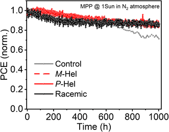
While photovoltaic performances were comparable, the stability of perovskite solar cells improved upon modulation (Fig. 4 and S27†). This was likely due to the increased hydrophobicity evidenced by contact angle measurements (Fig. S28†). Specifically, the contact angle between the water droplet and the perovskite surface increased upon modulating the perovskites, which suggests an increase in the hydrophobicity of the surface. This is expected to contribute to protecting the underlying perovskites from degradation upon exposure to moisture and improve contact with the hole-transporting material. Accordingly, the evolution of the photovoltaic characteristics at the maximum power point during continuous device operation indicated improved operational stabilities of the modulated devices compared to the control ones (Fig. 4). While the control devices lost more than 30% of their initial performances after 1000 h, the modulated systems maintained over 80% of their initial efficiency for more than 1000 h, corroborating the impact of helical modulation on the operational stabilities of perovskite solar cells and stimulating further investigations.
 | ||
| Fig. 4 Operational stability of perovskite solar cells (4 devices tested per condition). Maximum power point (MPP) tracking was measured with the unencapsulated device under full solar illumination (AM 1.5 G, 100 mW cm−2 under nitrogen at 25 °C). Other photovoltaic metrics are shown in Fig. S27.† | ||
Conclusions
In summary, we have assessed the utility of chiral helicene assemblies as interfacial modulators between the perovskite absorber and hole-transporting material in perovskite solar cells. In contrast to the previous reports on the beneficial effects of chiral assemblies, we do not identify any substantial contribution of the chiral moieties to the resulting photovoltaic performances. Instead, we observe differences in the performance between the racemic and enantiopure layers, with a benefit for the racemic system. Moreover, using modulators at the interface improves operational stabilities. While the performances could be further optimised, the results challenge the perspective on the role of chiral helical modulation in perovskite photovoltaics, stimulating further investigation toward realizing the potential of this approach.Data availability
Data is available at https://zenodo.org/records/11234499 under Creative Commons Attribution-ShareAlike 4.0 International license.Author contributions
The project was conceptualized by J. V. M. and J. C., who supervised the synthesis and characterization of the helicene modulators by S. K., while G. A., M. A., H. Z., and M. A. R.-P. characterized the perovskite materials and devices. N. V. performed the chiral HPLC separations. P. Z. performed the X-ray scattering measurements with the support of G. A. under the supervision of A. H. and F. S., whereas F. E. performed the PL/TRPL characterizations and the analysis of the optoelectronic loss mechanisms. D. M. D. performed the PL analysis in the magnetic field under the supervision of B. E., whereas S. M. Z. was involved in the discussion, and M. G. directed the study. All the authors contributed to the manuscript.Conflicts of interest
There are no conflicts to declare.Acknowledgements
This project received funding from the European Union's Horizon 2020 Research and Innovation Program under grant agreement no. 764047. J. V. M. acknowledges the SNSF grant no. 193174. M. A. acknowledges King Abdulaziz City for Science and Technology (KACST) for the fellowship. The work of D. D. and B. E. is part of the Dutch Research Council (NWO) project no. KICH1.ED02.20.007 performed at the institute AMOLF. The authors are grateful to Olivier Ouellette (EPFL) for support with the PL spectroscopy and data analysis. Parts of the research were done at SOLEIL (Paris, France). The authors gratefully acknowledge support by Andrea Resta and Alessandro Coati from beamline SIXS (SOLEIL). We acknowledge funding from the BMBF (ERUM-Pro) project 05K19VTA and thank Niels Scheffczyk and Leonard Simeonov for experimental support.References
- A. K. Jena, A. Kulkarni and T. Miyasaka, Chem. Rev., 2019, 119, 3036–3103 CrossRef CAS PubMed.
- R. Wang, M. Mujahid, Y. Duan, Z.-K. Wang, J. Xue and Y. Yang, Adv. Funct. Mater., 2019, 29, 1808843 CrossRef CAS.
- M. V. Khenkin, E. A. Katz, A. Abate, G. Bardizza, J. J. Berry, C. Brabec, F. Brunetti, V. Bulović, Q. Burlingame, A. Di Carlo, R. Cheacharoen, Y.-B. Cheng, A. Colsmann, S. Cros, K. Domanski, M. Dusza, C. J. Fell, S. R. Forrest, Y. Galagan, D. Di Girolamo, M. Grätzel, A. Hagfeldt, E. Hauff, H. Hoppe, J. Kettle, H. Köbler, M. S. Leite, S. F. Liu, Y.-L. Loo, J. M. Luther, C.-Q. Ma, M. Madsen, M. Manceau, M. Matheron, M. McGehee, R. Meitzner, M. K. Nazeeruddin, A. F. Nogueira, Ç. Odabaşı, A. Osherov, N.-G. Park, M. O. Reese, F. De Rossi, M. Saliba, U. S. Schubert, H. J. Snaith, S. D. Stranks, W. Tress, P. A. Troshin, V. Turkovic, S. Veenstra, I. Visoly-Fisher, A. Walsh, T. Watson, H. Xie, R. Yıldırım, S. M. Zakeeruddin, K. Zhu and M. Lira-Cantu, Nat. Energy, 2020, 5, 35–49 CrossRef.
- J. Wei, Q. Wang, J. Huo, F. Gao, Z. Gan, Q. Zhao and H. Li, Adv. Energy Mater., 2020, 77, 2002326 Search PubMed.
- K. Domanski, J.-P. Correa-Baena, N. Mine, M. K. Nazeeruddin, A. Abate, M. Saliba, W. Tress, A. Hagfeldt and M. Grätzel, ACS Nano, 2016, 10, 6306–6314 CrossRef CAS PubMed.
- K. Domanski, B. Roose, T. Matsui, M. Saliba, S.-H. Turren-Cruz, J.-P. Correa-Baena, C. R. Carmona, G. Richardson, J. M. Foster, F. De Angelis, J. M. Ball, A. Petrozza, N. Mine, M. K. Nazeeruddin, W. Tress, M. Grätzel, U. Steiner, A. Hagfeldt and A. Abate, Energy Environ. Sci., 2017, 10, 604–613 RSC.
- K. Domanski, E. A. Alharbi, A. Hagfeldt, M. Grätzel and W. Tress, Nat. Energy, 2018, 3, 61–67 CrossRef CAS.
- J. V. Milić, N. Arora, M. I. Dar, S. M. Zakeeruddin and M. Grätzel, Adv. Mater. Interfaces, 2018, 356, 1800416 CrossRef.
- J. V. Milić, D. J. Kubicki, L. Emsley and M. Grätzel, Chimia, 2019, 73, 317–323 CrossRef PubMed.
- S. Shao and M. A. Loi, Adv. Mater. Interfaces, 2019, 7, 1901469 CrossRef.
- S. Y. Kim, S. J. Cho, S. E. Byeon, X. He and H. J. Yoon, Adv. Energy Mater., 2020, 131, 2002606 CrossRef.
- R. Naaman and D. H. Waldeck, J. Phys. Chem. Lett., 2012, 3, 2178–2187 CrossRef CAS PubMed.
- K. Michaeli, N. Kantor-Uriel, R. Naaman and D. H. Waldeck, Chem. Soc. Rev., 2016, 45, 6478–6487 RSC.
- R. Naaman, Y. Paltiel and D. H. Waldeck, Nat. Rev. Chem, 2019, 3, 250–260 CrossRef CAS.
- R. Naaman, Y. Paltiel and D. H. Waldeck, Acc. Chem. Res., 2020, 53, 2659–2667 CrossRef CAS PubMed.
- K. Michaeli and R. Naaman, J. Phys. Chem. C, 2019, 123, 17043–17048 CrossRef CAS.
- J. M. Abendroth, D. M. Stemer, B. P. Bloom, P. Roy, R. Naaman, D. H. Waldeck, P. S. Weiss and P. C. Mondal, ACS Nano, 2019, 13, 4928–4946 CrossRef CAS PubMed.
- G. Long, R. Sabatini, M. I. Saidaminov, G. Lakhwani, A. Rasmita, X. Liu, E. H. Sargent and W. Gao, Nat. Rev. Mater., 2020, 5, 423–429 CrossRef.
- H. Lu, J. Wang, C. Xiao, X. Pan, X. Chen, R. Brunecky, J. J. Berry, K. Zhu, M. C. Beard and Z. V. Vardeny, Sci. Adv., 2019, 5, eaay0571 CrossRef CAS PubMed.
- J. Ahn, S. Ma, J.-Y. Kim, J. Kyhm, W. Yang, J. A. Lim, N. A. Kotov and J. Moon, J. Am. Chem. Soc., 2020, 142, 4206–4212 CrossRef CAS PubMed.
- Z.-G. Yu, J. Phys. Chem. Lett., 2020, 11, 8638–8646 CrossRef CAS PubMed.
- Z. Huang, B. P. Bloom, X. Ni, Z. N. Georgieva, M. Marciesky, E. Vetter, F. Liu, D. H. Waldeck and D. Sun, ACS Nano, 2020, 14, 10370–10375 CrossRef CAS PubMed.
- N. Xu, A. Zheng, Y. Wei, Y. Yuan, J. Zhang, M. Lei and P. Wang, Chem. Sci., 2020, 11, 3418–3426 RSC.
- Y. Dong, Y. Zhang, X. Li, Y. Feng, H. Zhang and J. Xu, Small, 2019, 15, 1902237 CrossRef PubMed.
- J. Ahn, E. Lee, J. Tan, W. Yang, B. Kim and J. Moon, Mater. Horiz., 2017, 4, 851–856 RSC.
- J. Ma, C. Fang, C. Chen, L. Jin, J. Wang, S. Wang, J. Tang and D. Li, ACS Nano, 2019, 13, 3659–3665 CrossRef CAS PubMed.
- Y. H. Kim, Y. Zhai, H. Lu, X. Pan, C. Xiao, E. A. Gaulding, S. P. Harvey, J. J. Berry, Z. V. Vardeny, J. M. Luther and M. C. Beard, Science, 2021, 371, 1129–1133 CrossRef CAS PubMed.
- M. Kettner, V. V. Maslyuk, D. Nürenberg, J. Seibel, R. Gutierrez, G. Cuniberti, K.-H. Ernst and H. Zacharias, J. Phys. Chem. Lett., 2018, 9, 2025–2030 CrossRef CAS PubMed.
- V. Kiran, S. P. Mathew, S. R. Cohen, I. Hernández Delgado, J. Lacour and R. Naaman, Adv. Mater., 2016, 28, 1957–1962 CrossRef CAS.
- R. Rodríguez, C. Naranjo, A. Kumar, P. Matozzo, T. K. Das, Q. Zhu, N. Vanthuyne, R. Gómez, R. Naaman, L. Sánchez and J. Crassous, J. Am. Chem. Soc., 2022, 144, 7709–7719 CrossRef PubMed.
- N. Hellou, C. Jahier-Diallo, O. Baslé, M. Srebro-Hooper, L. Toupet, T. Roisnel, E. Caytan, C. Roussel, N. Vanthuyne, J. Autschbach, M. Mauduit and J. Crassous, Chem. Commun., 2016, 52, 9243–9246 RSC.
- N. Hellou, M. Srebro-Hooper, L. Favereau, F. Zinna, E. Caytan, L. Toupet, V. Dorcet, M. Jean, N. Vanthuyne, J. A. G. Williams, L. Di Bari, J. Autschbach and J. Crassous, Angew. Chem., Int. Ed., 2017, 129, 8348–8351 CrossRef.
- D. Schweinfurth, M. Zalibera, M. Kathan, C. Shen, M. Mazzolini, N. Trapp, J. Crassous, G. Gescheidt and F. Diederich, J. Am. Chem. Soc., 2014, 136, 13045–13052 CrossRef CAS PubMed.
- J. V. Milić, C. Schaack, N. Hellou, F. Isenrich, R. Gershoni-Poranne, D. Neshchadin, S. Egloff, N. Trapp, L. Ruhlmann, C. Boudon, G. Gescheidt, J. Crassous and F. Diederich, J. Phys. Chem. C, 2018, 122, 19100–19109 CrossRef.
- M. A. Ruiz Preciado, D. J. Kubicki, A. Hofstetter, L. McGovern, M. H. Futscher, A. Ummadisingu, R. Gershoni-Poranne, S. M. Zakeeruddin, B. Ehrler, L. Emsley, J. V. Milić and M. Grätzel, J. Am. Chem. Soc., 2020, 142, 1645–1654 CrossRef CAS PubMed.
- T.-S. Su, F. T. Eickemeyer, M. A. Hope, F. Jahanbakhshi, M. Mladenović, J. Li, Z. Zhou, A. Mishra, J.-H. Yum, D. Ren, A. Krishna, O. Ouellette, T.-C. Wei, H. Zhou, H.-H. Huang, M. D. Mensi, K. Sivula, S. M. Zakeeruddin, J. V. Milić, A. Hagfeldt, U. Rothlisberger, L. Emsley, H. Zhang and M. Grätzel, J. Am. Chem. Soc., 2020, 142, 19980–19991 CrossRef CAS PubMed.
- H. Zhang, F. T. Eickemeyer, Z. Zhou, M. Mladenović, F. Jahanbakhshi, L. Merten, A. Hinderhofer, M. A. Hope, O. Ouellette, A. Mishra, P. Ahlawat, D. Ren, T.-S. Su, A. Krishna, Z. Wang, Z. Dong, J. Guo, S. M. Zakeeruddin, F. Schreiber, A. Hagfeldt, L. Emsley, U. Rothlisberger, J. V. Milić and M. Grätzel, Nat. Commun., 2021, 12, 3383 CrossRef CAS PubMed.
- P. Josse, L. Favereau, C. Shen, S. Dabos-Seignon, P. Blanchard, C. Cabanetos and J. Crassous, Chem.–Eur. J., 2017, 23, 6277–6281 CrossRef CAS PubMed.
- Y. Yang, B. Rice, X. Shi, J. R. Brandt, R. Correa da Costa, G. J. Hedley, D.-M. Smilgies, J. M. Frost, I. D. W. Samuel, A. Otero-de-la-Roza, E. R. Johnson, K. E. Jelfs, J. Nelson, A. J. Campbell and M. J. Fuchter, ACS Nano, 2017, 11, 8329–8338 CrossRef CAS PubMed.
- T. Kirchartz, J. A. Márquez, M. Stolterfoht and T. Unold, Adv. Energy Mater., 2020, 10, 1904134 CrossRef CAS.
- M. Kim, J. Jeong, H. Lu, T. K. Lee, F. T. Eickemeyer, Y. Liu, I. W. Choi, S. J. Choi, Y. Jo, H.-B. Kim, S.-I. Mo, Y.-K. Kim, H. Lee, N. G. An, S. Cho, W. R. Tress, S. M. Zakeeruddin, A. Hagfeldt, J. Y. Kim, M. Grätzel and D. S. Kim, Science, 2022, 375, 302–306 CrossRef CAS PubMed.
- Z. Wang, T. Ma, J. Wang, S. Zhu, M. Zhang and M. Guo, Ceram. Int., 2024, 50, 7528–7537 CrossRef CAS.
Footnotes |
| † Electronic supplementary information (ESI) available. See DOI: https://doi.org/10.1039/d4na00027g |
| ‡ Authors have contributed equally to this work. |
| § H. Z. is presently affiliated with State Key Laboratory of Photovoltaic Science and Technology, Shanghai Frontiers Science Research Base of Intelligent Optoelectronics and Perception, Institute of Optoelectronics, Fudan University, Shanghai, China. |
| This journal is © The Royal Society of Chemistry 2024 |
