
Designing a novel Eu2+-doped hafnium-silicate phosphor for an energy-down-shift layer of CsPbI3 solar cells
Yixin
Li
,
Shichuan
Wang
and
Yuhua
Wang
 *
*
Department of Materials Science, School of Materials and Energy, Key Laboratory of Special Function Materials and Structure Design of Ministry of Education, National and Local Joint Engineering Laboratory for Optical Conversion Materials and Technology of National Development and Reform Commission, Lanzhou University, Lanzhou 730000, P. R. China. E-mail: wyh@lzu.edu.cn
First published on 21st January 2022
Abstract
The excessive carbon discharge and low utilization efficiency of solar energy are still the biggest challenges in the world. A series of Eu2+ doped K2HfSiO5 phosphors were synthesized and applied in CsPbI3 perovskite solar cells. Under the excitation of ultraviolet and near ultraviolet light in the range of 300–450 nm, K2HfSiO5:Eu2+ exhibits emission in the visible range of 450–650 nm. Due to their strong absorption in the ultraviolet region and high quantum efficiency, K2HfSiO5:Eu2+ phosphors could be used to fabricate an energy-down-shift layer for solar cells. When spin-coated with the layer, the value of the short-circuit current of the packaged CsPbI3 solar cell increased, resulting in the enhancement of the power conversion efficiency by 2.19%. In addition, other basic properties of K2HfSiO5:Eu2+ phosphors such as photoluminescence, cathodoluminescence and stability have also been studied. All the results indicate that the energy-down-shift layer made using K2HfSiO5:Eu2+ phosphors has a positive effect on improving the performance of CsPbI3 perovskite solar cells.
1. Introduction
In recent years, a luminescence energy-down-shift (EDS) layer for solar cells has received much attention because of its obvious light conversion effect.1–3 By converting the light that is useless for solar cells (ultraviolet (UV) or infrared (IR) light) into the useful visible or near infrared light, the EDS layers allow solar cells to produce more carriers, thus improving their power conversion efficiency (PCE).4–6 Therefore, researching and developing EDS layers for solar cells are of great significance for the utilization of solar energy and clean energy.Among several types of solar cells, CsPbI3 perovskite solar cells have aroused interest due to their desirable band gap (about 1.73 eV), strong light absorption and outstanding photoelectric properties.7–9 CsPbI3 is considered to be one of the materials with the most potential as a new photovoltaic material for the next generation. According to some existing reports, inorganic quantum dots, carbon dots, up-conversion phosphors and metal clusters could serve as EDS layers for CsPbI3 solar cells.5,10–12 In these studies, although the performance of the solar cells has been enhanced to a certain extent, numerous shortcomings still exist. For example, the synthetic process of quantum dots is very complex, relating to many toxic raw materials which are harmful to human health and have a poor stability when set in an air environment. Besides, the photoluminescence quantum yield of most EDS layers made by up-conversion phosphors is very low, which affects the PCE of solar cells. Furthermore, though metal nano cluster luminescent materials have a high quantum efficiency, their fabrication cost is so high that they are not suitable for large-scale application. Hence, it is necessary for us to search for a novel light-conversion material which could be applied to the EDS layer for CsPbI3 solar cells with low costs and convenience of preparation.
As is well known, the range of the solar spectrum is from UV to IR light. However, the CsPbI3 solar cells cannot effectively utilize UV light because the photoelectric reaction in this region is weak. Instead, it has a strong photoelectric effect in the visible range (400–800 nm).13,14 As a type of light conversion material, phosphors have many advantages such as suitable size, excellent luminous efficiency, preferable stability, intense absorption in the UV region and low energy consumption.15–18 Consequently, phosphors with a down-conversion (DC) effect could better satisfy with the requirements of the EDS layer for CsPbI3 solar cells.19
It is worth mentioning that Eu2+ doped phosphors generally exhibit a broad-band emission according to the 4f–5d transition, so that they have outstanding luminescence features.20 Most part of Eu2+ activated phosphors which can be used in the EDS layer are nitrides such as CaAlSiN3:Eu2+, SrSi2O2N2:Eu2+ and (Ca,Sr)2Si5N8:Eu2+, Tm3+; they all have a favourable luminescence performance.21–23 However, it is very hard to synthesize nitrides because of their rigorous preparation conditions (high temperature and high pressure) and because the cost of their fabrication process is tremendously high. Silicate based phosphors are a superior choice; many of them have tremendous potential for photoluminescence and cathodoluminescence materials such as NaScSi2O6:Eu2+, RbNa3(Li3SiO4)4:Eu2+ and Sr3SiO5:Eu2+ because of their luminescence properties, splendid chemical and physical stability and so on.24–26 Thus, when combining with polyvinyl pyrrolidone (PVP), the luminescence performance of the silicate phosphor will not be influenced due to its great stability. In addition, silicates are easily available and low cost, widely used in basic research studies.27–29 In this work, we had prepared a K2HfSiO5:Eu2+ phosphor via replacing Zr in K2ZrSiO5:Eu2+ with Hf through the solid-state reaction. The highest internal quantum efficiency was nearly about 60% and the thermal stability was greatly improved.30 Then the K2HfSiO5:Eu2+ phosphor was successfully applied onto the CsPbI3 perovskite solar cells as an EDS layer. It is found that both short-circuit current (Jsc) and PCE are distinctly increasing. Meanwhile, the cathodoluminescence properties of the K2HfSiO5:Eu2+ phosphor were also explored, demonstrating that it has the potential for multifunctional application.
2. Experimental
Phosphor preparation
The K2HfSiO5:Eu2+ phosphor was fabricated through the high temperature solid-state method. The initial raw materials were K2CO3 (A.R), HfO2 (≥99.9%), SiO2 (A.R.) and Eu2O3 (99.99%). They were mixed together in a stoichiometric ratio, and 3 wt% H3BO3 was used as the flux. The mixture was ground homogeneously with alcohol for 20 minutes and then put into several alumina crucibles. The heating rate was set to 3 °C min−1. After calcination in a tube furnace at 1120 °C for 6 h in a reduced atmosphere (H2![[thin space (1/6-em)]](https://www.rsc.org/images/entities/char_2009.gif) :N2 = 5:95), the products were taken out and cooled down to room temperature and ground again for further analysis.
:N2 = 5:95), the products were taken out and cooled down to room temperature and ground again for further analysis.
EDS layer fabrication
The crude materials of the EDS layer were K2HfSiO5:0.02Eu2+ phosphor, PVP and ethanol. They were weighed according to the mass ratio of 1:10:50, and then PVP and ethanol were added into a beaker for stirring. After PVP dissolves, the K2HfSiO5:0.02Eu2+ phosphor was added into the beaker and stirring was continued for another 30 minutes. Finally, the EDS layer solution in the middle of the beaker was spin-coated on the near light side of the CsPbI3 solar cells in a glove box at 2000 rpm for 30 s at room temperature.
Device fabrication
Precursor solution preparation: all experiments were carried out in a glove box that was filled with N2. CsI and PbI2 were weighed according to the stoichiometric ratio in the container, 0166 g DAMI and 1 ml DMF were weighed, respectively; DMF-d7 was added according to the volume ratio of 5%, and magnetic stirring was carried out for more than 6 h.Packaged solar cell preparation: the precursor solution was spin coated on the TiO2/FTO surface which was treated with peroxide plasma for 35 s at 3000 rpm. Then it was annealed at 210 °C for 10 min to obtain the CsPbI3 film. After this, the device was assembled as an EDS layer/FTO/TiO2/CsPbI3 film/spiro-OMeTAD/electrode structure, and finally the spin coated CsPbI3 device was obtained.
Measurements and characterization
The phase of the instrument of X-ray powder diffraction (XRD) was Bruker D2 PHASER X-ray diffractometer with Cu Kα radiation. The range of the measured 2θ was 10–80°, the set step length was 0.03° and the counting time was 0.1 s per step. The XRD Rietveld refinement result of the K2HfSiO5 host was obtained using the General Structure Analysis System (GSAS).31 Both the morphology and Energy Dispersive X-Ray (EDX) spectra were obtained using a scanning electron microscope (SEM) and a transmission electron microscope (TEM). Density functional theory (DFT) was used to calculate the band structure with the help of the Cambridge Serial Total Energy Packet (CASTEP) code.32 The diffuse reflectance spectra (DRS) were obtained using an UV-vis spectrophotometer (PE-Lambda 950) and BaSiO4 powders were used as a reference. The photoluminescence (PL) and photoluminescence excitation (PLE) spectra and decay curves were detected using a FLS-920T fluorescence spectrophotometer. At the same time, thermal stability was tested with the same PL equipment and a TAP-02 heating device was added. The cathodoluminescence (CL) properties of K2HfSiO5:Eu2+ phosphors were measured using a Mp-Micro-S instrument. The current density–voltage (I–V) curves were recorded via the illumination of an AM 1.5G (100 mW cm−2) solar simulator (Enlitech). The external quantum efficiency (EQE) spectra were measured using a Quantum efficiency tester (QE-R, Enlitech).3. Results and discussion
Crystal structure and phase information
The XRD Rietveld refinement was introduced to acquire the detailed crystal structure of K2HfSiO5. For the sake of acquiring the phase information, K2ZrSiO5 was set as an initial model. The refinement results are shown in Fig. 1(a). The calculated data agree well with the experimental data and the refined factors are Rwp = 8.52%, Rp = 7.67% and χ2 = 1.31, respectively. These parameters illustrated that the results of refinement have a referential value. The total refinement crystal data are shown in Table 1. It could be known that K2HfSiO5 is a monoclinic crystal system and its space group belongs to p121/c1(14), and the atom coordinates are listed in Table 2.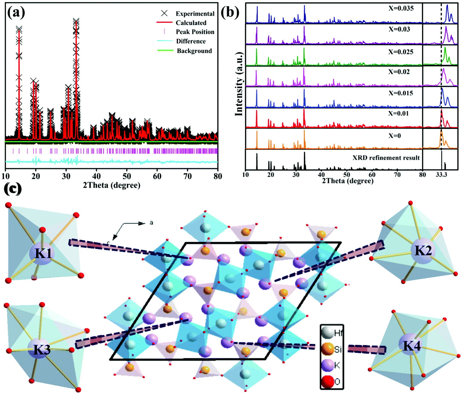 | ||
| Fig. 1 (a) The K2HfSiO5 host Rietveld refinement result; (b) XRD patterns of K2HfSiO5:xEu2+ (0.00 ≤ x ≤ 0.035); and (c) the crystal structure sketch map of K2HfSiO5 and the different coordination surroundings of K+. | ||
| Formula | K2HfSiO5 |
|---|---|
| Crystal system | Monoclinic |
| Z | 8 |
| V | 975.51(32) Å3 |
| Space-group | P121/c1 (14) |
| P | 4.97 g cm−3 |
| A | 14.10(18) Å |
| B | 5.67 Å |
| C | 14.09 Å |
| A | 90.00° |
| B | 90.00° |
| Γ | 119.98° |
| χ 2 | 1.311 |
| R wp | 8.52% |
| R p | 7.67% |
| Atom | Wyckoff | x/a | y/b | z/c |
|---|---|---|---|---|
| K1 | 4e | 0.291(5) | 0.778(6) | 0.144(8) |
| K2 | 4e | 0.075(3) | 0.752(6) | 0.126(4) |
| K3 | 4e | 0.195(6) | 0.221(2) | 0.332(6) |
| K4 | 4e | 0.430(6) | 0.250(3) | 0.071(7) |
| Hf1 | 4e | 0.065(8) | 0.739(3) | 0.369(2) |
| Hf2 | 4e | 0.434(2) | 0.235(8) | 0.309(4) |
| Si1 | 4e | 0.161(3) | 0.244(9) | 0.088(6) |
| Si2 | 4e | 0.338(4) | 0.761(2) | 0.394(6) |
| O1 | 4e | 0.127(8) | 0.102(4) | 0.461(5) |
| O2 | 4e | 0.289(9) | 0.254(3) | 0.150(9) |
| O3 | 4e | 0.408(9) | 0.789(13) | 0.041(8) |
| O4 | 4e | 0.212(9) | 0.714(7) | 0.362(5) |
| O5 | 4e | 0.092(14) | 0.303(9) | 0.129(7) |
| O6 | 4e | 0.378(9) | 0.596(22) | 0.338(15) |
| O7 | 4e | 0.134(2) | 0.934(7) | 0.027(3) |
| O8 | 4e | 0.363(1) | 0.064(8) | 0.392(6) |
| O9 | 4e | 0.007(12) | 0.474(4) | 0.272(8) |
| O10 | 4e | 0.492(10) | 0.966(3) | 0.263(1) |
According to the XRD patterns of K2HfSiO5:xEu2+ (0 ≤ x ≤ 0.35) samples shown in Fig. 1(b), with the increasing amounts of the introduced Eu ions, all the diffraction peaks are in accordance with the refinement result. The Eu2+ ions are considered to occupy the position of K+ because the values of the ionic radii of Eu2+ (1.17 Å, coordination number (CN) = 6; 1.2 Å, CN = 7) are close to those of K+ (1.38 Å, CN = 6; 1.46 Å, CN = 7), and much higher than those of Hf4+ (0.71 Å, CN = 6; 0.76 Å, CN = 7). It is worth noting in the partial enlarged patterns that the position of the diffraction peak at 33.3° gradually shifts to larger 2θ with Eu2+ doping. This phenomenon could be attributed to the fact that smaller radius (Eu2+) ions occupy the site of the larger ions (K+). According to the Bragg formula, when the smaller ions substituted the larger ones, the crystal lattice would shrink, leading to an increase of θ.33 All the above results indicate that Eu ions are successfully doped into the K2HfSiO5 host and there is no impurity phase.
Fig. 1(c) displays the structure of K2HfSiO5. One [SiO4]4− tetrahedron is connected with another [HfO6]8− octahedron by sharing one O2−, and one [Hf2O11]14− unit also consisted of two [HfO6]8− octahedra. A variety of polyhedron pairs constituting a 3D framework of K2HfSiO5 and the isolated K+ act as cations which could be substituted by doped ions. There are four different coordination surroundings of K+ (K1, CN = 6; K2, CN = 6; K3, CN = 7 and K4, CN = 7) and as listed in Table 3, the average bond lengths of K1–O, K2–O, K3–O and K4–O are 2.658 Å, 2.587 Å, 2.714 Å and 2.663 Å, respectively.
| Bond | Distance |
|---|---|
| K1–O(CN = 6) | 2.658(6) |
| K2–O(CN = 6) | 2.587(3) |
| K3–O(CN = 7) | 2.714(9) |
| K4–O(CN = 7) | 2.663(2) |
Fig. 2(a) reveals the SEM image of K2HfSiO5:0.02Eu2+ particles. The shape of the sample is irregular rod distribution, the ranges of the length and diameter are 10–15 μm and 2–5 μm, respectively. The SEM mapping image of the sample is shown in Fig. 2(b). It could be seen from the image that K, Hf, Si, O and Eu elements are detected and uniformly distributed on the selected particle surface. In addition, TEM and the High-Resolution Transmission Electron Microscope (HRTEM) graphs of K2HfSiO5:0.02Eu2+ are shown in Fig. 2(c). The stable crystal lattice could be seen clearly and the distance between two adjacent crystal planes is 0.4515 nm, which corresponds to the (111) crystal plane. The different element compositions of K2HfSiO5:0.02Eu2+ are exhibited in Fig. 2(d). There are no other elements in the sample (the C peak is attributed to the instrument) and it could be observed from the insight table that the stoichiometric ratio of each element has exactly constituted K2HfSiO5. These characterization methods demonstrated the successful preparation of K2HfSiO5:Eu.
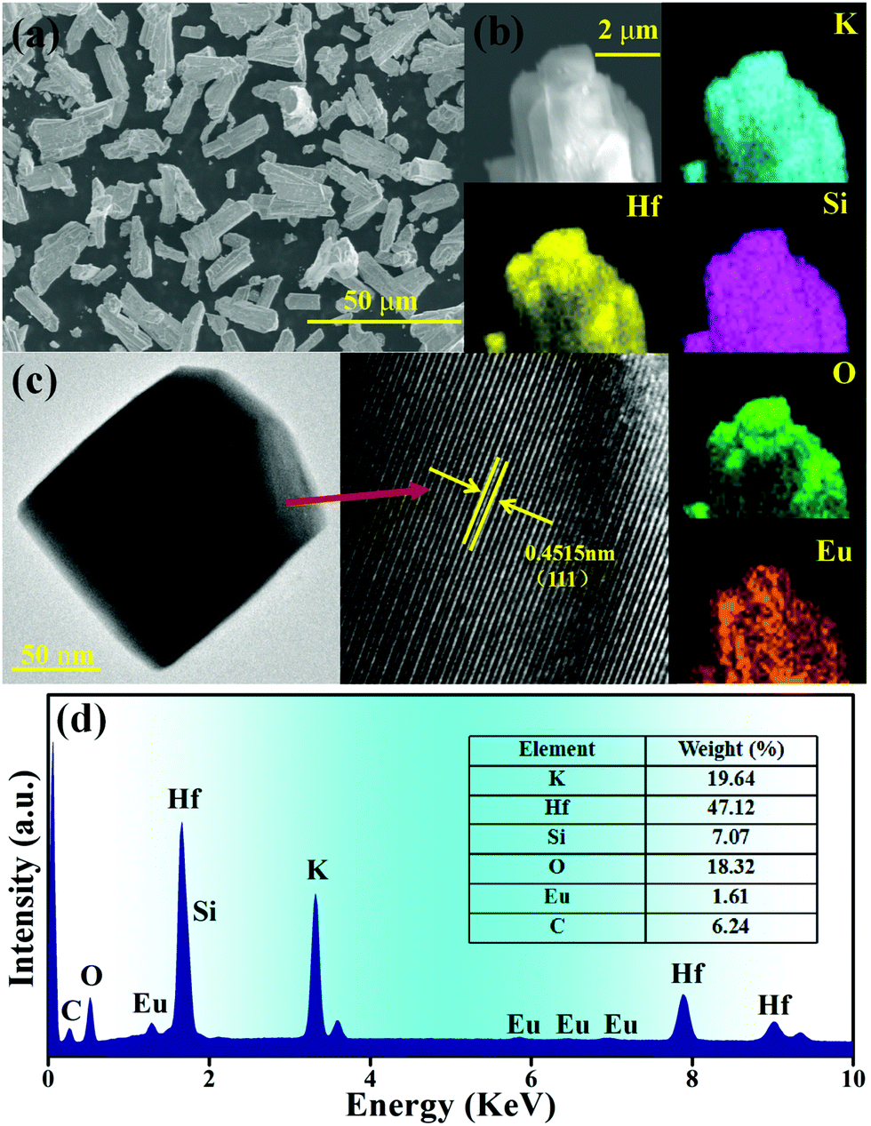 | ||
| Fig. 2 (a) SEM image of K2HfSiO5:0.02Eu2+; (b) SEM mapping (K, Hf, Si, O and Eu) of K2HfSiO5:0.02Eu2+; (c) TEM and HTEM images of one K2HfSiO5:0.02Eu2+ particle; and (d) EDX spectrum of K2HfSiO5:0.02Eu2+. | ||
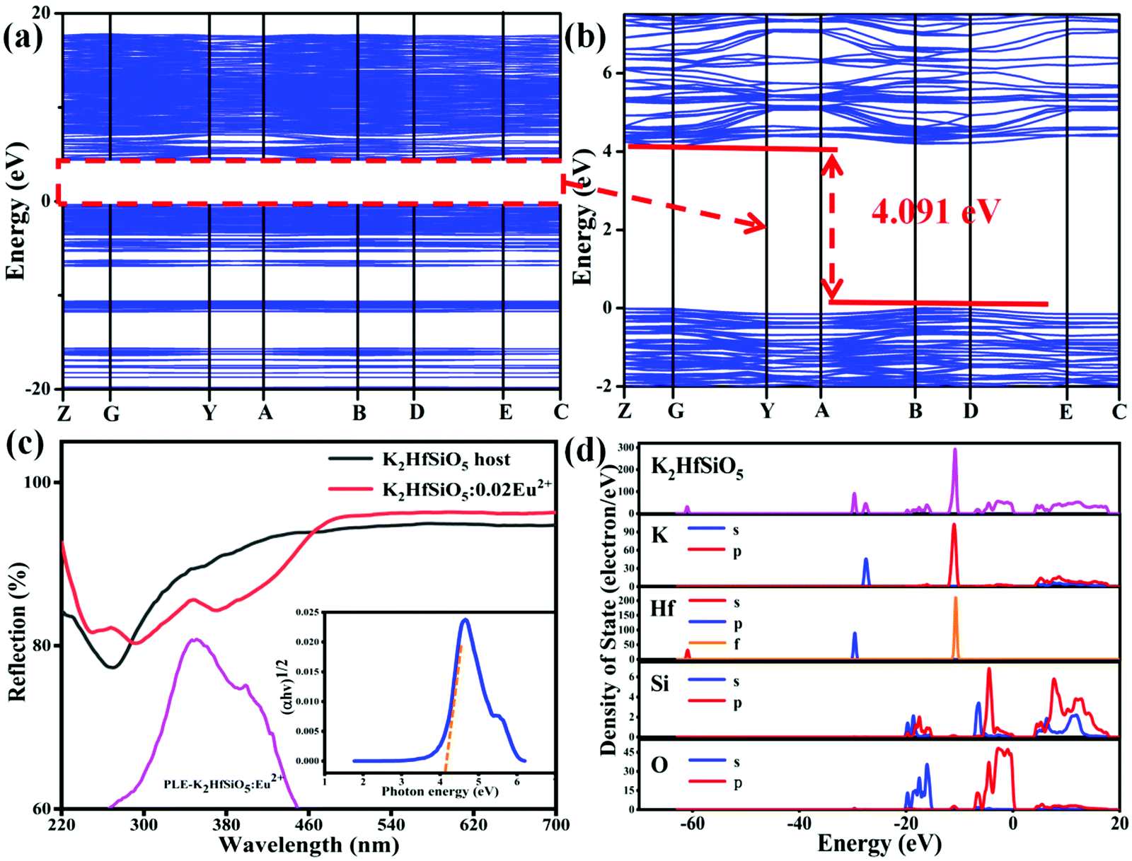
The calculated band structure of K2HfSiO5 is shown in Fig. 3(a) and (b) according to the refined crystallographic results. It could be observed that K2HfSiO5 has an indirect band;34 the maximum position of the valence band (VB) is located at point B and the minimum position of conduction band (CB) is located at point G. The calculated bandgap of K2HfSiO5 is 4.091 eV. The diffuse reflectance spectrum (DRS) of the K2HfSiO5 host displayed in Fig. 3(c) was taken to judge whether the calculation value is reliable. The optical bandgap of the K2HfSiO5 host could be obtained using the following formulae:
| (αhν)1/2 = A(hν − Eg) | (1) |
 | (2) |
 | ||
| Fig. 3 (a) and (b) Band structure of K2HfSiO5; (c) the DRS spectra of Eu2+ doped and host of K2HfSiO5 (the inset shows the relationship between photon energy and (αhν)1/2 of the K2HfSiO5 host); (d) total and partial density of states of K2HfSiO5. | ||
In these equations, α refers to the absorption co-efficient, hν is the incident photon energy, A is constant, and n = 1/2 corresponding to an indirect bandgap. As depicted in Fig. 3(c), the obtained optical bandgap of K2HfSiO5 is 4.125 eV. The value of the calculated bandgap is close to that of the optical bandgap, indicating the reliability of the calculation. This value illustrated that the 4f65d ↔ 4f7 energy level transition of Eu2+ has little influence on the VB and CB of K2HfSiO5.35
Fig. 3(d) displays the calculated total Density of States (DOS) and partial Density of States (PDOS) of K2HfSiO5. The graph shows that the upper VB is mainly composed of the p-states of O element. The lower VB (−10 eV to −30 eV) involves the K s, p-states, Hf p-states, Si s, p-states and O s-states. These characteristics indicate the strong sp-hybridization of O-Hf and O-Si, which could be frequently seen in silicate inorganic hosts.36 The CB is chiefly composed of K p-states. The DOS shows that the formation of the CB and VB includes the participation of all elements. All the above results show that K2HfSiO5 could be used as a potential host of luminescent materials.
Photoluminescence properties
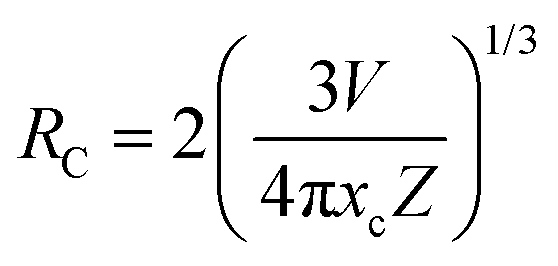
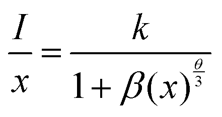
Fig. 4(a) shows the PL spectra and PLE spectra of K2HfSiO5:0.02Eu2+. When monitoring at 513 nm, a broad excitation band ranging from 250–480 nm has been detected, with a peak at 360 nm. Under 360 nm wavelength excitation, the K2HfSiO5:0.02Eu2+ phosphor shows a cyan-green light emission, exhibiting a wide emission band in the range of 400–650 nm with the maximum value located at 513 nm because of the 5d–4f energy transition of Eu2+.37,38 However, several sharp peaks appear in the range of 550–650 nm, which could be attributed to the energy transition of Eu3+. In order to explore the reason of these peaks, the emission spectrum monitored at 394 nm is given in Fig. 4(b). It is found that the characteristic peak of Eu3+ was detected despite its intensity being weak. The sharp peaks at 570 nm, 586 nm, 598 nm, 615 nm and 650 nm correspond to the 5D0–7Fj (j = 0, 1, 2, 3 and 4) energy transition of Eu3+, respectively. This result illustrates that a small amount of Eu3+ was not reduced to Eu2+ in K2HfSiO5:Eu2+. Owing to the existence of Eu3+, the K2HfSiO5:Eu phosphor is not suitable for light emitting diode (LED) devices. However, for the EDS layer, the characteristic emission of Eu3+ could increase the efficiency of the solar spectral conversion for solar cells.39–41 The PL spectra of various concentrations of Eu2+ doped K2HfSiO5 are shown in Fig. 4(c). The optimum doping concentration is nearly about 2% with an internal quantum efficiency of 59.5% at this time. With the increase of Eu2+ concentration, the possibility of non-radiative energy transfer between Eu2+ was increasing, which would lead to concentration quenching.42 The inset photo shows the time-resolved PL (TRPL) spectra of K2HfSiO5:0.02Eu2+. It could be observed that the shape of TRPL spectra is consistent with that of PL spectra. Distinctly, different decay times have been detected when monitoring at the same wavelength, indicating that energy transfer occurs between different Eu2+ ions and further proving that there exist several luminescence centers in the K2HfSiO5:Eu2+ phosphor.43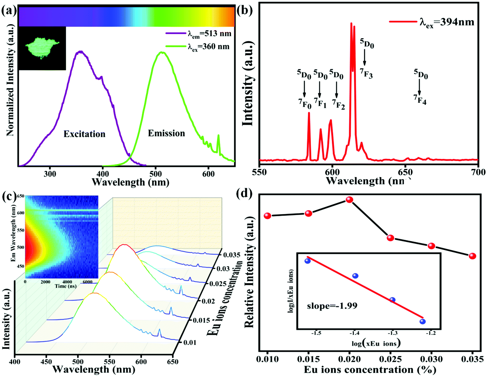 | ||
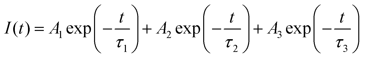
| Fig. 4 (a) PLE and PL spectra of K2HfSiO5:0.02Eu2+ (the inset shows the phosphor image under 365 nm ultraviolet light); (b) PL spectrum of K2HfSiO5:0.02Eu2+ under 394 nm excitation; (c) the emission spectra of K2HfSiO5:xEu2+ (0.01 ≤ x ≤ 0.35) (the inset represents the TRPL spectra); and (d) the relative emission intensity of K2HfSiO5:xEu2+ (0.01 ≤ x ≤ 0.35) samples (the inset shows the curve of log(x) and log(I/x).). | ||
There are three energy transfer methods among Eu2+ ions: radiation re-absorption, exchange interactions, or electric multipolar interactions.42 It could be observed from Fig. 4(a) that the emission and excitation bands have a little overlap area, so that the effect of re-absorption is small. The parameter of critical distance (Rc) has been introduced to further confirm which mechanism of energy transfer between the different Eu2+ in K2HfSiO5:0.02Eu2+. When Rc ≤ 5 Å, the energy transfer mechanism is exchange interactions, otherwise it may be electric multipolar interactions. The value of Rc could be calculated using the following equation:44
 | (3) |
 | (4) |
The factor x refers to the doping concentration of Eu2+, θ = 6, 8 or 10 representing the dipole–dipole, dipole–quadrupole and quadrupole–quadrupole interactions, respectively. What's more, k and β are constants. Fig. 4(d) inset shows the fitting line of log (x) and log (I/x). The slope of this line represents θ/3. For K2HfSiO5:xEu2+ (0.01 ≤ x ≤ 0.035) samples, the calculated result of θ is close to 6, demonstrating that the energy transfer interaction type of K2HfSiO5:Eu2+ is dipole–dipole.
To further probe the reason for the concentration quenching of the K2HfSiO5:Eu2+ phosphor, Fig. 5 depicts the decay curves of the K2HfSiO5:xEu2+ (0.01 ≤ x ≤ 0.035) samples and all the decay curves could be fitted by the following formula[30]:
 | (5) |
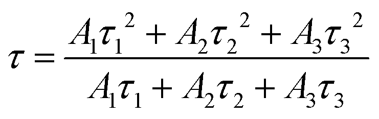 | (6) |
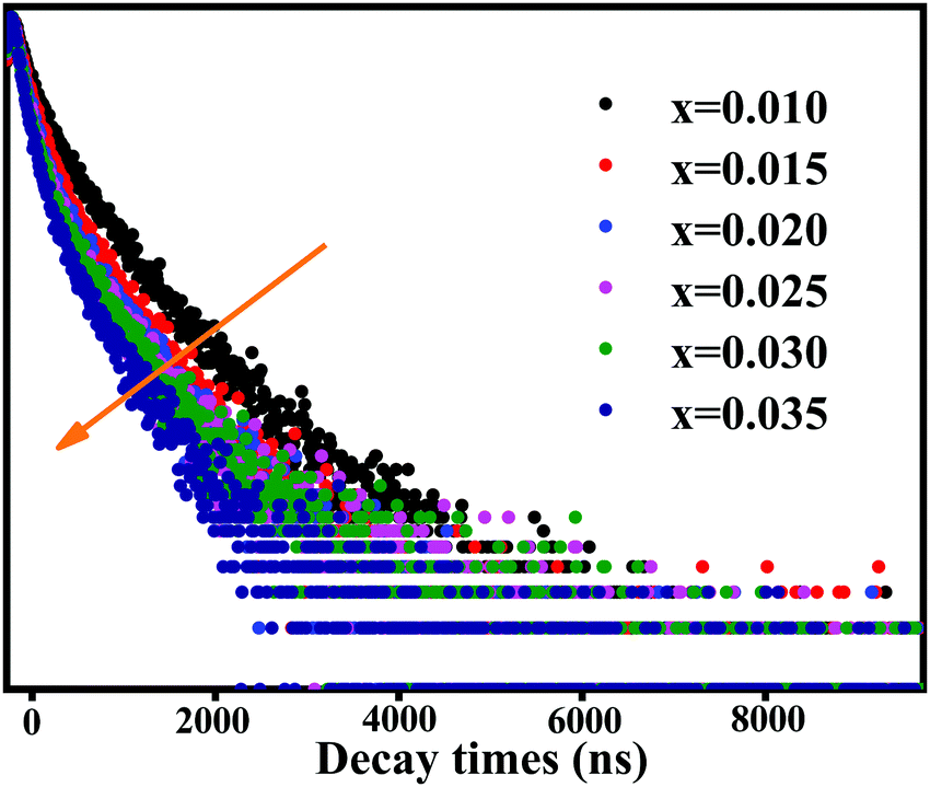 | ||
| Fig. 5 The decay curves of the K2HfSiO5:xEu2+ (0.01 ≤ x ≤ 0.035) samples. | ||
According to this formula, the average decay times of different concentrations of Eu2+ doping samples are 512, 505, 486, 478, 468 and 455 ns, separately. With the increase of Eu2+, the decay time of K2HfSiO5:Eu2+ keeps decreasing. This could be ascribed to the fact that the distance between the activators becomes shorter with the increase of the Eu2+ doping amount. Therefore, non-radiative energy transfer is more likely to occur in K2HfSiO5:Eu2+, leading to concentration quenching of Eu2+.46
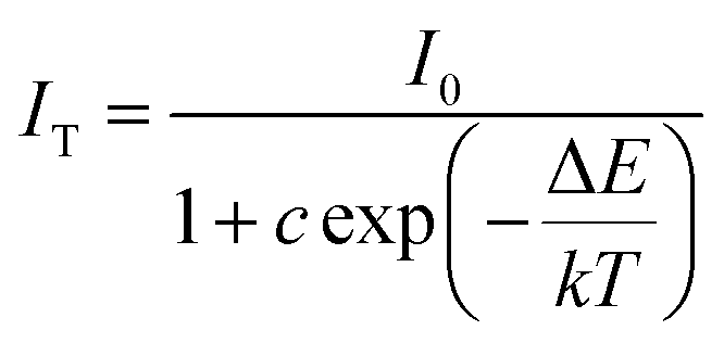
The thermal stability of K2HfSiO5:Eu2+ is shown in Fig. 6(a). It could be found that the emission intensity decreased with the temperature increase from 25 °C to 200 °C; the position of emission almost doesn’t shift. Fig. 6(b) shows the relative emission intensity with a linear increase in temperature. When it reached 150 °C, K2HfSiO5:0.02Eu2+ could still retain about 81.2% of its initial emission intensity. This result shows that the thermal stability of K2HfSiO5:Eu2+ is apparently higher than that of Na2HfSiO5:Eu2+ (retains 45% at 150 °C) and K2ZrSiO5:Eu2+ (retains 19.4% at 150 °C) phosphors. To understand the reason why the K2HfSiO5:Eu2+ phosphor has great thermal stability, the activation energy (ΔE) could be calculated according to the Arrhenius equation:47
 | (7) |
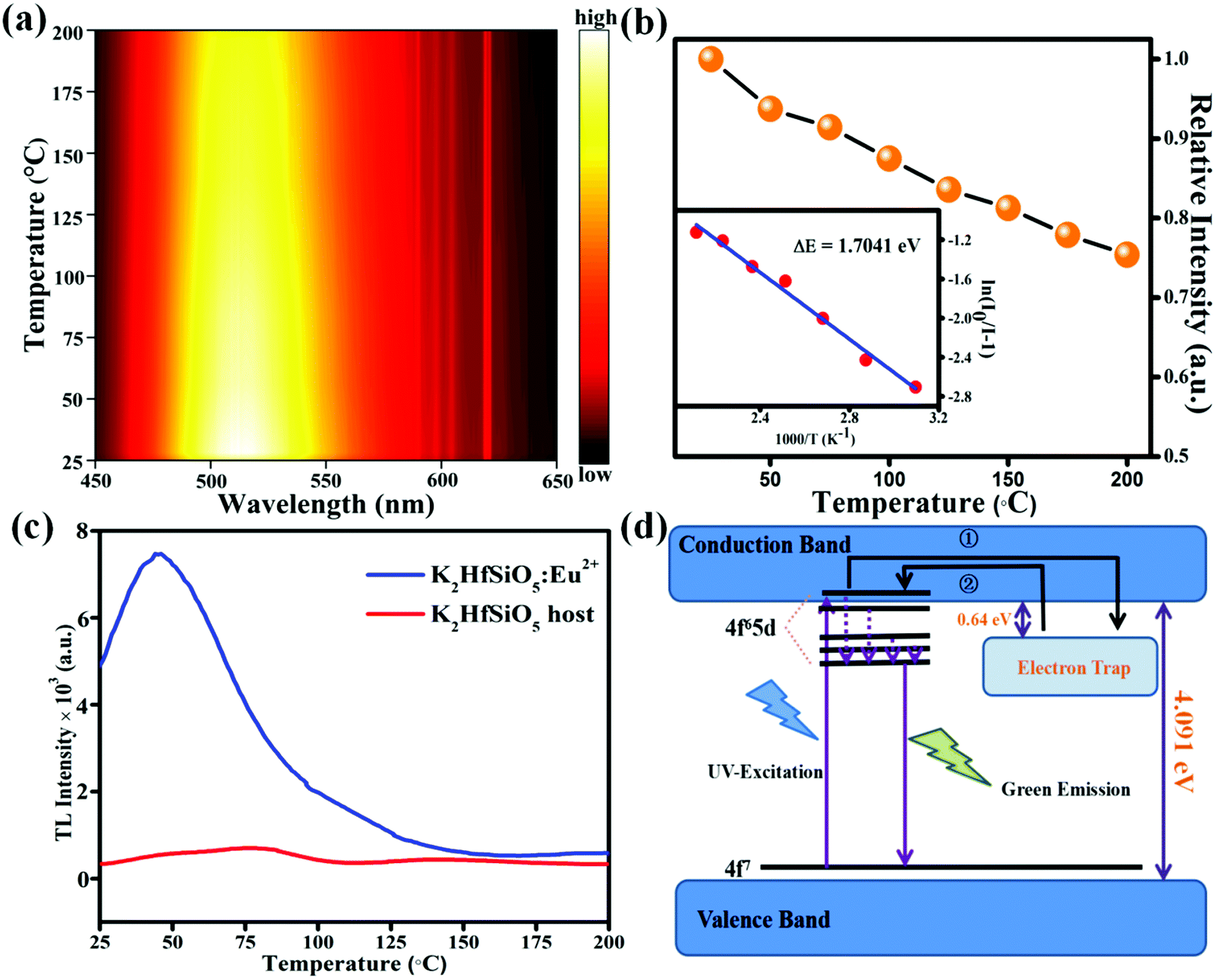 | ||
| Fig. 6 (a) Temperature dependent luminescence spectra of K2HfSiO5:0.02Eu2+ phosphor from 25 to 200 °C; (b) the relative emission intensity of K2HfSiO5:0.02Eu2+ at different temperatures (the inset shows the fitting activation energy of K2HfSiO5:0.02Eu2+); (c) the thermoluminescence (TL) curves of K2HfSiO5:0.02Eu2+ and K2HfSiO5 host; and (d) the energy level diagram of Eu2+ in K2HfSiO5. | ||
The thermoluminescence curves of the K2HfSiO5 host and K2HfSiO5:Eu2+ are shown in Fig. 6(c). It could be obviously seen that there exists an electron trap at about at 50 °C in K2HfSiO5:Eu2+. The trap depth could be estimated using the following formula:
 | (8) |
Cathodoluminescence properties
The cathodoluminescence (CL) performance is vital for the display of radar, television and oscilloscope.49–51Fig. 7(a) and (b) show the SEM and CL mapping images of one K2HfSiO5:0.02Eu2+ particle. These graphs demonstrate that luminescence centers are distributed on the particle evenly.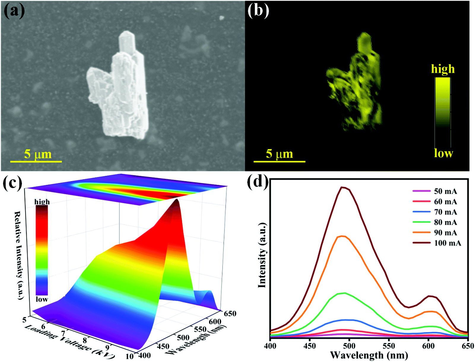 | ||
| Fig. 7 The SEM image (a) and CL mapping (b) of one K2HfSiO5:0.02Eu2+ particle; (c) the CL intensity of K2HfSiO5:0.02Eu2+ with various voltage (4–9 kV); and (d) the CL spectra of K2HfSiO5:0.02Eu2+ with different current (50–100 mA). | ||
Fig. 7(c) represents the CL spectra of K2HfSiO5:0.02Eu2+ under increasing voltage. The shape of the CL spectra is similar to the PL spectra which are shown in Fig. 4(a). When the current remains at 60 mA, the CL intensity of K2HfSiO5:0.02Eu2+ continuously increases with the growing voltage (5–10 kV). This phenomenon could be explained by the electron penetration depth and the value could be calculated using the following formula:52
 | (9) |
In this case, A is the molecular weight of K2HfSiO5, Z indicates the atomic number, ρ refers to the density, and E is the loading voltage (kV). For K2HfSiO5:Eu2+, A = 364.77, Z = 207 and ρ = 4.97 g cm−3. The calculated electron penetration depths are 25.45 (6 kV), 92.31 (8 kV) and 307.69 (10 kV) nm, respectively. Moreover, as shown in Fig. 7(d), the CL intensity also increases with different currents varying from 50–100 mA. The deeper the electron penetration depth, the more luminescence centers detected, leading to an increase of the CL intensity.
The anti-degradation properties of K2HfSiO5:0.02Eu2+ have been tested under certain conditions (6 kV, 60 mA) shown in Fig. 8. Obviously, the CL intensity decreases slowly with the electron bombardment from 10 to 90 min. It is well known that graphite carbon will accumulate in the process of high current density electron beam irradiation. This accumulation will not only prevent low-energy electrons from reaching the phosphor particles, but also aggravate surface charging which leads to the decrease of CL intensity.53 It can be observed from Fig. 8 that the CL intensity still remains about 80.12% of the initial intensity, indicating that the CL stability of K2HfSiO5:0.02Eu2+ is perfect. Meanwhile, the color stability and peak position of K2HfSiO5:0.02Eu2+ are almost unchanged. All the above results demonstrate that the K2HfSiO5:Eu2+ phosphor possesses outstanding CL properties and has potential application in CL devices.
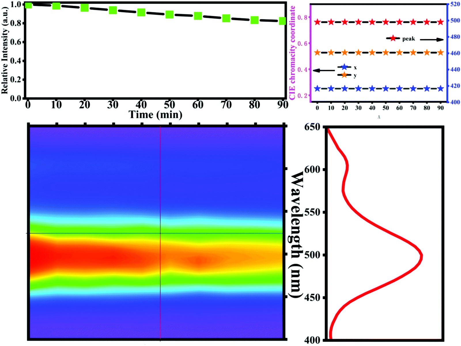 | ||
| Fig. 8 The anti-degradation properties and the relative intensity of K2HfSiO5:0.02Eu2+ under sustained electron bombardment (the top right corner represents the change of CIE coordinates and peak position). | ||
Applications
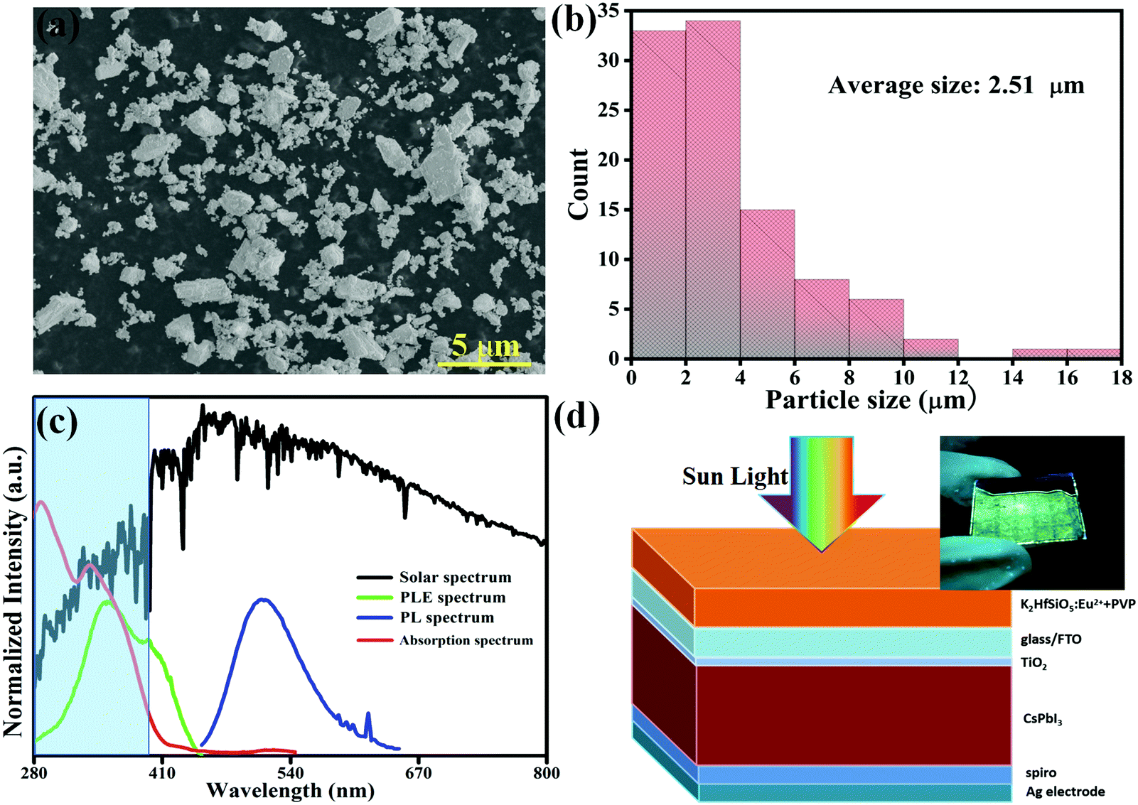 | ||
| Fig. 9 (a) The SEM image of K2HfSiO5:0.02Eu2+ particles for the energy-down-shift layer; (b) the average size of K2HfSiO5:0.02Eu2+ phosphor; (c) solar spectrum, emission spectrum of K2HfSiO5:0.02Eu2+ under 360 nm excitation, excitation spectrum monitored at 513 nm and the absorption spectrum of coated solar cell; and (d) schematic structure of CsPbI3 solar cells coated with the EDS layer. | ||
In order to more intuitively illustrate the successful application of the EDS layer on CsPbI3 solar cells, the EDS layer was spin coated on FTO and characterized by SEM as shown in Fig. 10(a). According to the vertical view, the K2HfSiO5:Eu2+ phosphor in the EDS layer is evenly distributed in the film-forming agent PVP, and there is no obvious agglomeration of phosphor particles. The side view clearly shows that the EDS layer is a film with an average thickness of nearly about 2 μm. It could be seen from the reflection spectra in Fig. 10(b) that the reflectivity of the solar cells coated with the EDS layer has decreased. Therefore, it can be concluded that part of the UV light has been converted into visible light. The I–V curves are measured as shown in Fig. 10(c). When coated with this EDS layer, the JSC shows an increasing tendency after coated with the EDS layer. To further verify the effect of the K2HfSiO5:Eu2+ phosphor EDS layer, the external quantum efficiency (EQE) spectra are shown in Fig. 10(d). In the range of UV light, the value of uncoated sample is lower than that of the coated sample. However, the EQE curves of the two samples are similar in other ranges of light. Therefore, it can be concluded that the increase of Jsc is related to the application of the energy transfer layer. PCE could be calculated from the parameters shown in Table 4:
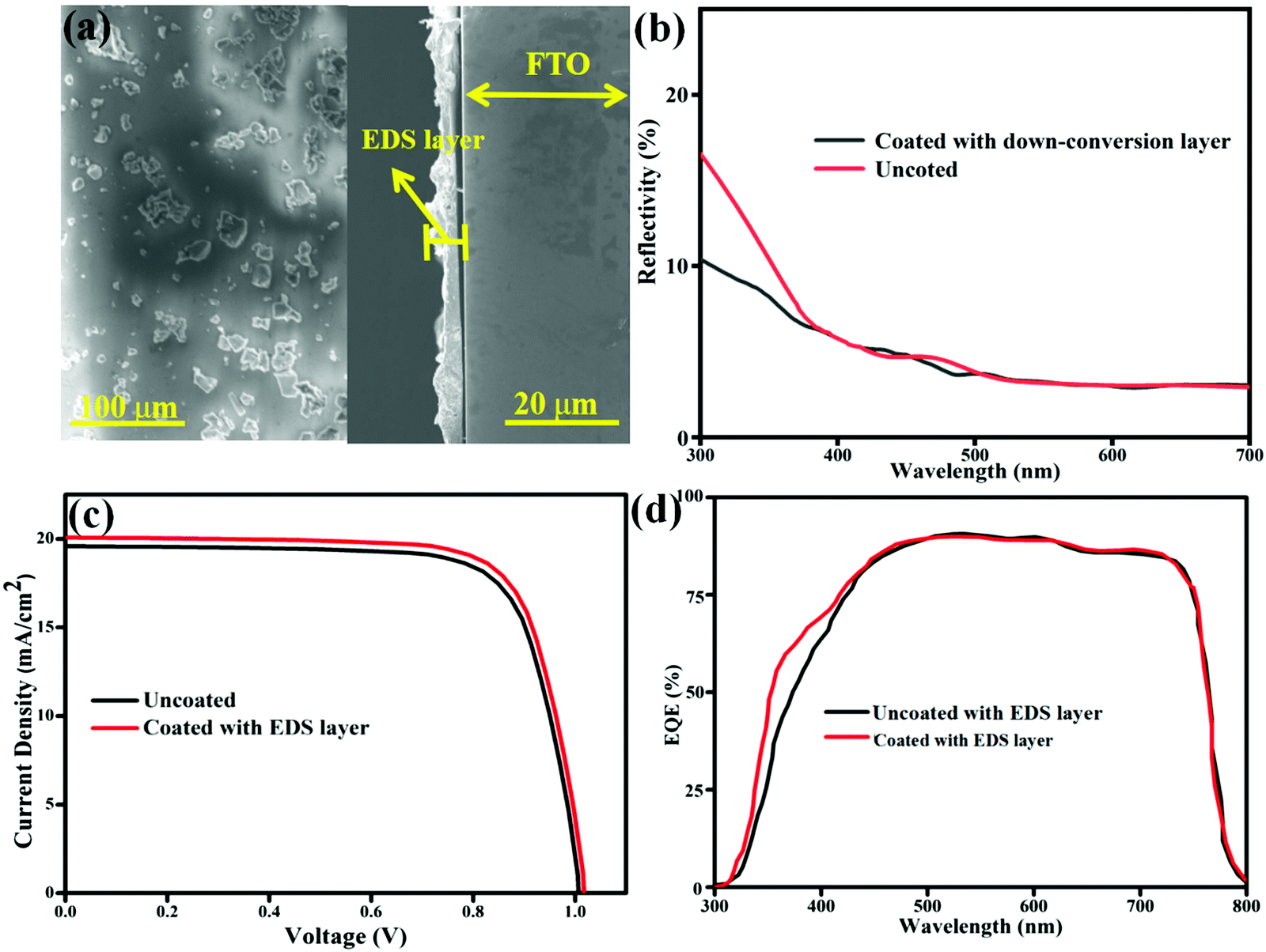 | ||
| Fig. 10 (a) SEM images of the EDS layer in vertical and side views; (b) reflection spectra of solar cells; (c) I–V curves of solar cells; (d) the EQE spectra of CsPbI3 solar cells with coated and uncoated solar cells. | ||
| Sample | V oc (V) | J SC (mA cm−2) | Fill factor (%) | PCE (%) | ΔPCE (%) |
|---|---|---|---|---|---|
| Bare cell | 1.007 | 19.77 | 72.47 | 16.35 | 2.19 |
| Coated cell | 1.012 | 20.05 | 72.48 | 16.73 |
This result shows that the CsPbI3 solar cells coated with the EDS layer present a higher PCE value of 16.83%, with an amplification of 2.19% compared with that of the bare cell. These results indicate that K2HfSiO5:0.02Eu2+ could be used as an EDS layer to improve the PCE of CSPbI3 solar cells. At the same time, it also provides the possibility for the combination of the luminescence material and perovskite solar cell technology.
4. Conclusions
In this work, a series of K2HfSiO5:xEu2+ (0.01 ≤ x ≤ 0.035) phosphors were successfully designed and synthesized for the first time. The structure, morphology and bandgap were investigated in detail. Under 360 nm excitation, the K2HfSiO5:0.02Eu2+ phosphor emits a high efficiency cyan-green light and the peak is located at 513 nm. After the feasibility analysis, we packaged the CsPbI3 solar cells coated with the K2HfSiO5:0.02Eu2+ phosphor EDS layer and the major electrochemical parameters were increased. Under the sustained electron-beam excitation, the K2HfSiO5:0.02Eu2+ phosphor shows excellent anti-degradation properties and a perfect color stability. In addition, since the K2HfSiO5:Eu2+ phosphor has potential for multifunctional application, we can imagine that in future, we can use the K2HfSiO5:Eu2+ EDS layer to improve the photoelectric conversion rate of solar cells, and then apply the electric energy to cathodoluminescence devices fabricated using the K2HfSiO5:Eu2+ phosphor. All the above results offer us a novel way to achieve effective utilization of solar energy.Conflicts of interest
There are no conflicts to declare.References
- M. Ali, R. Riaz, S. Bae, H.-S. Lee, S. H. Jeong and M. J. Ko, Layer-by-Layer self-assembly of hollow nitrogen-doped carbon quantum dots on cationized textured crystalline silicon solar cells for an efficient energy down-shift, ACS Appl. Mater. Interfaces, 2020, 12, 10369–10381 CrossRef CAS PubMed
.
- R. Riaz, M. Ali, T. Maiyalagan, A. S. Anjum, S. Lee, M. J. Ko and S. H. Jeong, Dye-sensitized solar cell (DSSC) coated with energy down shift layer of nitrogen-doped carbon quantum dots (N-CQDs) for enhanced current density and stability, Appl. Surf. Sci., 2019, 483, 425–431 CrossRef CAS
- B. Ren and C. Jiang, Designing a multi-quantum-dot-doped wavelength down-shifting model of c-Si solar cells by using machine learning, Appl. Opt., 2020, 59, 985–990 CrossRef CAS PubMed
- J. M. Ball, S. D. Stranks, M. T. Hörantner, S. Hüttner, W. Zhang, E. J. Crossland, I. Ramirez, M. Riede, M. B. Johnston and R. H. Friend, Optical properties and limiting photocurrent of thin-film perovskite solar cells, Energy Environ. Sci., 2015, 8, 602–609 RSC
- H. Bian, Q. Wang, S. Yang, C. Yan, H. Wang, L. Liang, Z. Jin, G. Wang and S. F. Liu, Nitrogen-doped graphene quantum dots for 80% photoluminescence quantum yield for inorganic γ-CsPbI3 perovskite solar cells with efficiency beyond 16%, J. Mater. Chem. A, 2019, 7, 5740–5747 RSC
- M. Jalalah, Y.-H. Ko, F. A. Harraz, M. Al-Assiri and J.-G. Park, Enhanced efficiency and current density of solar cells via energy-down-shift having energy-tuning-effect of highly UV-light-harvesting Mn2+-doped quantum dots, Nano Energy, 2017, 33, 257–265 CrossRef CAS
- X. Zhang, H. Huang, X. Ling, J. Sun, X. Jiang, Y. Wang, D. Xue, L. Huang, L. Chi, J. Yuan and W. Ma, Homojunction Perovskite Quantum Dot Solar Cells with over 1 μm-Thick Photoactive Layer, Adv. Mater., 2021, 33, 2105977 Search PubMed
- J. Yuan, X. Zhang, J. Sun, R. Patterson, H. Yao, D. Xue, Y. Wang, K. Ji, L. Hu, S. Huang, D. Chu, T. Wu, J. Hou and J. Yuan, Hybrid Perovskite Quantum Dot/Non-Fullerene Molecule Solar Cells with Efficiency Over 15%, Adv. Funct. Mater., 2021, 2101272 CrossRef CAS
- J. Yuan, N. Rujisamphan, W. Ma, J. Yuan, Y. Li and S. T. Lee, Perspective on the perovskite quantum dots for flexible photovoltaics, J. Energy Chem., 2021, 62, 505–507 CrossRef
- Z. Li, J. Guo, Z. Li, W. Han, G. Ren, C. Liu, L. Shen and W. Guo, Incorporating self-assembled silane-crosslinked carbon dots into perovskite solar cells to improve efficiency and stability, J. Mater. Chem. A, 2020, 8, 5629–5637 RSC
- L. Liang, M. Liu, Z. Jin, Q. Wang, H. Wang, H. Bian, F. Shi and S. Liu, Optical management with nanoparticles for a light conversion efficiency enhancement in inorganic γ-CsPbI3 solar cells, Nano Lett., 2019, 19, 1796–1804 CrossRef CAS PubMed
-
P. V. Kamat, Emergence of new materials for light–energy conversion: perovskites, metal Clusters, and 2-D Hybrids, ACS Publications, 2014 Search PubMed
- S. C. Liu, Y. Yang, Z. Li, D. J. Xue and J. S. Hu., GeSe thin-film solar cells, Mater. Chem. Front., 2020, 4(3), 775–787 RSC
- W. T. Li, Q. S. Liu, K. Jin, M. Cheng, F. Hao, W. Q. Wu, S. J. Liu, Z. Xiao, S. F. Yang, A. W. Shi and L. M. Ding, Fused-ring phenazine building blocks for efficient copolymer donors, Mater. Chem. Front., 2020, 1454–1458 RSC
- P. Pust, P. J. Schmidt and W. Schnick, A revolution in lighting, Nat. Mater., 2015, 14, 454–458 CrossRef CAS PubMed
- H. A. Höppe, Recent developments in the field of inorganic phosphors, Angew. Chem., Int. Ed., 2009, 48, 3572–3582 CrossRef PubMed
- B. S. Richards, Luminescent layers for enhanced silicon solar cell performance: Down-conversion, Sol. Energy Mater. Sol. Cells, 2006, 90, 1189–1207 CrossRef CAS
- P. Du, J. Ma, Q. Zhu and J. G. Li, Phase evolution, structure, and up-/down-conversion luminescence of Li6CaLa2Nb2O12: Yb3+/RE3+ phosphors (RE = Ho, Er, Tm), J. Am. Ceram. Soc., 2020, 103, 2674–2685 CrossRef CAS
- L. Gao, Y. Yan, Y. Li and T. Ma, Comparison of Physical Isolation on Large Active Area Perovskite Solar Cells, Chem. Res. Chin. Univ., 2020, 36, 1279–1283 CrossRef CAS
- X. Qin, X. Liu, W. Huang, M. Bettinelli and X. Liu, Lanthanide-activated phosphors based on 4f-5d optical transitions: theoretical and experimental aspects, Chem. Rev., 2017, 117, 4488–4527 CrossRef CAS PubMed
- Z. Hosseini, E. W. G. Diau, K. Mehrany and N. Taghavinia, Assessment of Luminescent Downshifting Layers for the Improvement of Light-Harvesting Efficiency in Dye-Sensitized Solar Cells, ChemPhysChem, 2014, 15, 3791–3799 CrossRef CAS PubMed
- Y.-C. Fang, P.-C. Kao, Y.-C. Yang and S.-Y. Chu, Two-step synthesis of SrSi2O2N2: Eu2+ green oxynitride phosphor: electron-phonon coupling and thermal quenching behavior, J. Electrochem. Soc., 2011, 158, J246 CrossRef CAS
- J. Wang, H. Zhang, B. Lei, H. Dong, H. Zhang, Y. Liu, M. Zheng and Y. Xiao, Optical energy storage properties of (Ca1−xSrx)2Si5N8: Eu2+,Tm3+ solid solutions, J. Am. Ceram. Soc., 2015, 98, 1823–1828 CrossRef CAS
- Z. Xia, Y. Zhang, M. S. Molokeev and V. V. Atuchin, Structural and luminescence properties of yellow-emitting NaScSi2O6: Eu2+ phosphors: Eu2+ site preference analysis and generation of red emission by codoping Mn2+ for white-light-emitting diode applications, The, J. Phys. Chem. C, 2013, 117, 20847–20854 CrossRef CAS
- H. Liao, M. Zhao, M. S. Molokeev, Q. Liu and Z. Xia, Learning from a mineral structure toward an ultra-narrow-band blue-emitting silicate phosphor RbNa3 (Li3SiO4)4: Eu2+, Angew. Chem., 2018, 130, 11902–11905 CrossRef
- J. K. Park, C. H. Kim, S. H. Park, H. D. Park and S. Y. Choi, Application of strontium silicate yellow phosphor for white light-emitting diodes, Appl. Phys. Lett., 2004, 84, 1647–1649 CrossRef CAS
- X. Xu, Q. Shao, L. Yao, Y. Dong and J. Jiang, Highly efficient and thermally stable Cr3+ -activated silicate phosphors for broadband near-infrared LED applications, Chem. Eng. J., 2020, 383, 123108 CrossRef CAS
- X. Tong, J. Han, R. Cai, Y. Xu, P. Wu, H. Zhou and X. Zhang, Multisite-occupancy-driven efficient multiple energy transfer: a straightforward strategy to achieve single-composition white-light emission in Ce3+-, Tb3+-, and Mn2+-doped silicate phosphors, Inorg. Chem., 2020, 59, 9838–9846 CrossRef CAS PubMed
- R. Nagaraj, A. Raja and S. Ranjith, Synthesis and luminescence properties of novel red-emitting Eu3+ ions doped silicate phosphors for photonic applications, J. Alloys Compd., 2020, 827, 154289 CrossRef CAS
- Q. Wu, J. Ding and J. Zhou, Insight into a Eu2+-activated zirconium-silicate yellow phosphor for multifunctional applications, Ceram. Int., 2020, 46, 20545–20552 CrossRef CAS
- B. H. Toby, EXPGUI, a graphical user interface for GSAS, J. Appl. Crystallogr., 2001, 34, 210–213 CrossRef CAS
- M. Segall, P. J. Lindan, M.a. Probert, C. J. Pickard, P. J. Hasnip, S. Clark and M. Payne, First-principles simulation: ideas, illustrations and the CASTEP code, J. Phys.: Condens. Matter, 2002, 14, 2717 CrossRef CAS
- O. Eritsyan, Diffraction reflection of light in a cholesteric liquid crystal in the presence of wave irreversibility and Bragg formula for media with nonidentical forward and return wavelengths, J. Exp. Theor. Phys., 2000, 90, 102–108 CrossRef CAS
- G. Cassabois, P. Valvin and B. Gil, Hexagonal boron nitride is an indirect bandgap semiconductor, Nat. Photonics, 2016, 10, 262–266 CrossRef CAS
- Q. Wei, J. Ding and Y. Wang, A novel wide-excitation and narrow-band blue-emitting phosphor with hafnium silicon multiple rings structure for photoluminescence and cathodoluminescence, J. Alloys Compd., 2020, 831, 154825 CrossRef CAS
- D. Magero, M. E. Casida, G. Amolo, N. Makau and L. Kituyi, Partial density of states ligand field theory (PDOS-LFT): Recovering a LFT-like picture and application to photoproperties of ruthenium(II) polypyridine complexes, J. Photochem. Photobiol., A, 2017, 348, 305–325 CrossRef CAS
- P. Dorenbos, Energy of the first 4f7 → 4f65d transition of Eu2+ in inorganic compounds, J. Lumin., 2003, 104, 239–260 CrossRef CAS
- E. Elzer, P. Strobel, V. Weiler, P. J. Schmidt and W. Schnick, Illuminating nitridoberylloaluminates: the highly efficient red-emitting phosphor Sr2 [BeAl3N5]: Eu2+, Chem. Mater., 2020, 32, 6611–6617 CrossRef CAS
- X. Yang, J. Chen, S. Zheng and C. Chen, A downshifting Eu3+ doped glass embedded with concave pyramid microstructure to improve the efficiency of silicon solar cell, J. Rare Earths, 2020, 38, 1158–1164 CrossRef CAS
- K. Jha and M. Jayasimhadri, Effective sensitization of Eu3+ and energy transfer in Sm3+/Eu3+ co-doped ZPBT glasses for CuPc based solar cell and w-LED applications, J. Lumin., 2018, 194, 102–107 CrossRef CAS
- J. Garcia, L. Bontempo, L. Gomez-Malagon and L. Kassab, Efficiency boost in Si-based solar cells using tellurite glass cover layer doped with Eu3+ and silver nanoparticles, Opt. Mater., 2019, 88, 155–160 CrossRef CAS
- D. L. Dexter and J. H. Schulman, Theory of concentration quenching in inorganic phosphors, J. Chem. Phys., 1954, 22, 1063–1070 CrossRef CAS
- R. Shi, L. Ning, Z. Wang, J. Chen, T. K. Sham, Y. Huang, Z. Qi, C. Li, Q. Tang and H. Liang, Zero-thermal quenching of Mn2+ red luminescence via efficient energy transfer from Eu2+ in BaMgP2O7, Adv. Opt. Mater., 2019, 7, 1901187 CrossRef CAS
- G. Blasse, Energy transfer in oxidic phosphors, Phys. Lett. A, 1968, 28, 444–445 CrossRef CAS
- D. L. Dexter, A theory of sensitized luminescence in solids, J. Chem. Phys., 1953, 21, 836–850 CrossRef CAS
- N. J. Johnson, S. He, S. Diao, E. M. Chan, H. Dai and A. Almutairi, Direct evidence for coupled surface and concentration quenching dynamics in lanthanide-doped nanocrystals, J. Am. Chem. Soc., 2017, 139, 3275–3282 CrossRef CAS PubMed
- K. Shioi, N. Hirosaki, R.-J. Xie, T. Takeda and Y. Q. Li, Photoluminescence and thermal stability of yellow-emitting Sr-α-SiAlON: Eu2+ phosphor, J. Mater. Sci., 2010, 45, 3198–3203 CrossRef CAS
- Q. Wei, J. Ding and Y. Wang, A novel tunable extra-broad yellow-emitting nitride phosphor with zero-thermal-quenching property, Chem. Eng. J., 2020, 386, 124004 CrossRef CAS
- J. Götze and U. Kempe, A comparison of optical microscope-and scanning electron microscope-based cathodoluminescence (CL) imaging and spectroscopy applied to geosciences, Mineral. Mag., 2008, 72, 909–924 CrossRef
- S. Meuret, Y. Auad, L. Tizei, H. Chang, F. Houdellier, M. Kociak and A. Arbouet, Time-resolved Cathodoluminescence in a Transmission Electron Microscope Applied to NV Centers in Diamond, Microsc. Microanal., 2020, 26, 2022–2023 CrossRef
- F. Ammari, N. Del-Solar-Velarde, R. Chapoulie and B. Bousquet, Chemometrics applied to cathodoluminescence images: a new approach to classify pre-Columbian artefacts from northern Peru, Environ. Sci. Pollut. Res., 2017, 24, 2205–2209 CrossRef CAS PubMed
- G. Li, C. Li, C. Zhang, Z. Cheng, Z. Quan, C. Peng and J. Lin, Tm3+ and/or Dy3+ doped LaOCl nanocrystalline phosphors for field emission displays, J. Mater. Chem., 2009, 19, 8936–8943 RSC
- P. Wen, S. Zhang, D. Li, J. Liu, L. Zhang, K. Zhou, M. Feng, A. Tian, F. Zhang and X. Gao, Identification of degradation mechanisms of blue InGaN/GaN laser diodes, J. Phys. D: Appl. Phys., 2015, 48, 415101 CrossRef
- Q. Wang, X. Zhang, Z. Jin, J. Zhang, Z. Gao, Y. Li and S. F. Liu, Energy-down-shift CsPbCl3: Mn quantum dots for boosting the efficiency and stability of perovskite solar cells, ACS Energy Lett., 2017, 2, 1479–1486 CrossRef CAS
- J. Jin, H. Li, W. Bi, C. Chen, B. Zhang, L. Xu, B. Dong, H. Song and Q. Dai, Efficient and stable perovskite solar cells through e-beam preparation of cerium doped TiO2 electron transport layer, ultraviolet conversion layer CsPbBr3 and the encapsulation layer Al2O3, Sol. Energy, 2020, 198, 187–193 CrossRef CAS
- Ç. Kırbıyık, A. Toprak, C. Başlak, M. Kuş and M. Ersöz, Nitrogen-doped CQDs to enhance the power conversion efficiency of perovskite solar cells via surface passivation, J. Alloys Compd., 2020, 832, 154897 CrossRef
- Y. Wang, Y. Chang, J. Zhang, G. Lu and Z. Wei, Semitransparent Flexible Organic Solar Cells, Chem. Res. Chin. Univ., 2020, 36, 343–350 CrossRef CAS
| This journal is © the Partner Organisations 2022 |