DOI:
10.1039/D1QM01586A
(Research Article)
Mater. Chem. Front., 2022,
6, 1026-1032
Controlling the charge carrier dynamics by modulating the orientation diversity of perovskites†
Received
7th December 2021
, Accepted 2nd March 2022
First published on 3rd March 2022
Abstract
Organic–inorganic halide perovskite-based solar cells have drastically improved in recent decades, with power conversion efficiencies of up to 25%. However, the fundamental photophysical properties underlying the outstanding performance have not been elucidated. Herein, we investigate the detailed photo-induced charge carrier dynamics over a wide time domain from sub-nanoseconds to microseconds, via time-correlated single photon counting and flash photolysis time-resolved microwave conductivity measurements. The structure of the perovskites significantly influences the whole periodic dynamics of mobile charge carriers. The mobility was considerably larger and the extraction to the transporting layer occurred more effectively in perovskites with higher orientation diversity than in highly oriented perovskites, resulting in higher efficiencies. The relationship between the orientation diversity of perovskites and their power conversion efficiency was investigated. Our work will be beneficial for the development of high-efficiency solar cell devices.
Introduction
Organic–inorganic halide perovskite solar cells (PSCs) have been spotlighted as a promising alternative to silicon-based solar cells. Significant improvements in device efficiencies have been achieved over the past few years.1–12 An unprecedented rise in the power conversion efficiency (PCE) of PSCs of over 25% has led to numerous studies to investigate the photophysical properties of perovskites. However, there is still a lack of fundamental understanding regarding the whole periodic dynamics of photo-induced charge carriers from the nanosecond to microsecond time scale. Recently, studies on mobile charge carriers within perovskites in the microsecond region have been conducted using flash photolysis time-resolved microwave conductivity (FP-TRMC) measurements.13–15 Saeki et al. found that enhanced charge carrier mobilities were achieved through morphological changes by adding bulky A-site cations, guanidinium (GA), for high-efficiency tin-based PSCs.13 Hutter et al. first revealed the temperature dependence of charge carrier mobilities and recombination rates for various perovskite materials.14 These studies have significantly broadened our understanding of the intrinsic photophysical properties of perovskites. Herein, we investigated detailed photo-induced charge carrier dynamics over a wide time window by combining FP-TRMC measurements with the time-correlated single photon counting (TCSPC) technique. As the TCSPC technique measures the radiative recombination rate in the nanosecond region and FP-TRMC measures all recombination rates from sub-micro to microseconds, these two measurements could be quite complementary. Thus, the combination of these two measurements is essential for understanding the whole periodic dynamics of photo-induced charge carriers. Consequently, they can be advantageous in the design of high-efficiency devices. In particular, by modulating the orientation diversity of perovskite films, we investigated the effects of structural diversity on charge carrier dynamics. Furthermore, we demonstrate that structural orientation diversity leads to improved PSC performance owing to increased charge carrier mobility and effective charge extraction to the electrodes. The increased orientation diversity of the perovskite film could release the micro-strain in the crystal structures, which could enhance the performance of the SPCs.16–18
Experimental section
Materials
Lead iodide (PbI2, 99.999%, anhydrous beads), lead bromide (PbBr2, 99.999%), methylammonium iodide (CH3NH3I, ≥99%, anhydrous), formamidinium iodide (CH(NH2)2I, ≥99%, anhydrous), methylammonium bromide (CH3NH3Br, ≥99%, anhydrous), N,N-dimethylformamide (DMF, 99.8%, anhydrous), dimethyl sulfoxide (DMSO, ≥99.9%, anhydrous), and all the other chemicals were purchased from Sigma Aldrich/Merck or Alfa Aesar. All materials were used as received without any treatment.
Perovskite film fabrication
To prepare the 1.2 M FAPbI3 (or MAPbI3, MAPbBr3) precursor solution, FAI (or MAI, MABr) is mixed with PbI2 (or PbBr2) in DMF![[thin space (1/6-em)]](https://www.rsc.org/images/entities/char_2009.gif) :DMSO mixed solvent (4:1 volume ratio) at room temperature. For the solution of (FAPbI3)0.85(MAPbBr3)0.15, prepared FAPbI3 and MAPbBr3 solutions were mixed with the corresponding volume ratio. All perovskite precursor solutions were prepared inside a nitrogen-filled glovebox. In the case of the perovskite solution that we used in this study, excess PbI2 (5 mol% to FAPbI3 or MAPbI3) was mixed with the prepared (FAPbI3)0.85(MAPbBr3)0.15 for the diverse orientation (D.O.) perovskite and (MAPbI3)0.85(MAPbBr3)0.15 for the highly oriented (H.O.) perovskite solution and stirred at room temperature for 2 h. Then a D.O. perovskite layer was deposited by spin-coating the prepared perovskite solution at 2000 and 6000 rpm for 20 and 30 s, respectively. During the last 15 s of the second spin-coating step, an anti-solvent of chlorobenzene (CB) was drop-cast. For H.O. perovskite, the perovskite solution was spun at 4000 rpm for 30 s and diethyl ether (DE) was used as an anti-solvent. The films were annealed on a hot plate at 100 °C for 30 min.
:DMSO mixed solvent (4:1 volume ratio) at room temperature. For the solution of (FAPbI3)0.85(MAPbBr3)0.15, prepared FAPbI3 and MAPbBr3 solutions were mixed with the corresponding volume ratio. All perovskite precursor solutions were prepared inside a nitrogen-filled glovebox. In the case of the perovskite solution that we used in this study, excess PbI2 (5 mol% to FAPbI3 or MAPbI3) was mixed with the prepared (FAPbI3)0.85(MAPbBr3)0.15 for the diverse orientation (D.O.) perovskite and (MAPbI3)0.85(MAPbBr3)0.15 for the highly oriented (H.O.) perovskite solution and stirred at room temperature for 2 h. Then a D.O. perovskite layer was deposited by spin-coating the prepared perovskite solution at 2000 and 6000 rpm for 20 and 30 s, respectively. During the last 15 s of the second spin-coating step, an anti-solvent of chlorobenzene (CB) was drop-cast. For H.O. perovskite, the perovskite solution was spun at 4000 rpm for 30 s and diethyl ether (DE) was used as an anti-solvent. The films were annealed on a hot plate at 100 °C for 30 min.
Perovskite solar cell fabrication
An FTO glass substrate (AGC Fabritech, TCO VU) was sequentially cleaned with toluene, acetone, and ethanol for 15 min each in an ultrasonic bath. Compact TiO2 (c-TiO2) was deposited using spray pyrolysis (∼50 nm) on the FTO substrate using a 12.5 mM titanium diisopropoxide bis(acetylacetonate) solution at 470 °C. On top of the c-TiO2 layer, 150 mg mL−1 of mesoporous TiO2 paste (meso-TiO2, Greatcell solar 30 NR-D) in ethanol was spin-coated at 4000 rpm for 12 s. The substrates were then annealed at 100 °C for 5 min followed by sintering at 500 °C for 30 min, producing a meso-TiO2 layer of ∼200 nm. Then, a perovskite layer was deposited by spin-coating the prepared perovskite solution, producing a capping perovskite layer of ∼700 nm on the meso-TiO2. (The same conditions are used for producing test structures with a perovskite film on glass only or the FTO substrate only.) For a solution of hole transport material (HTM), 520 mg mL−1 lithium bis(trifluoromethylsulfonyl)imide in acetonitrile (Li-TFSI) was prepared. Then, 72.3 mg of spiro-OMeTAD, 17.5 μL of a Li-TFSI solution, and 31.2 μL of 4-tert-butylpyridine were mixed in 1 mL chlorobenzene. This solution was spin-coated on the FTO/meso-TiO2/c-TiO2/perovskite substrate at 5000 rpm for 40 s, which gave ∼150 nm thickness of the spiro-OMeTAD layer. A 100 nm gold electrode was deposited by thermal evaporation. All films on meso-TiO2 were deposited in a nitrogen-filled glovebox.
Measurement and characterization
Steady-state absorption spectra were measured on a UV/Vis/NIR spectrometer (Varian, Cary5000) and fluorescence spectra were measured on a fluorescence spectrophotometer (Hitachi, F-7000/F-2500). Fluorescence spectra are spectrally corrected by using the correction factor of the fluorescence spectrophotometer. The surface morphology and cross-sectional images of perovskite thin films were investigated using a field-emission scanning electron microscopy (FE-SEM, JSM7500 and JSM-7100F, JEOL Ltd, Tokyo, Japan) with an accelerating voltage of 5–15 kV. The as-spun thin film on the glass substrate was coated with platinum (20 mA for 60 s) with a high-resolution sputter coater (208HR, Cressington Scientific Instruments Ltd, England, UK). X-ray diffraction patterns of thin films were obtained using a high-resolution X-ray diffractometer (HR-XRD, SmartLab, Rigaku, Tokyo, Japan) where Cu Kα radiation was used with a scan rate of 2° min−1. Other experimental details are described in the ESI.†
Results and discussion
Structural analysis according to orientation diversity
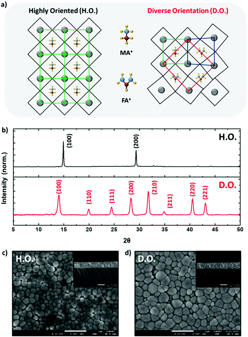
In this study, we synthesized H.O. perovskite films using only methylammonium (MA) as an A-site cation and D.O. perovskite films using both MA and formamidinium (FA) as A-site cations. As shown in Fig. 1a, when MA and FA are used as A-site cations, atoms within the perovskite crystal structure rearrange, inducing lattice extension (compared to only MA A-site cations), resulting in increased orientation diversity along multiple directions. To confirm the modulated orientation diversity of perovskite films upon intercalation of FA cations into the perovskite structure, the perovskite films were subjected to XRD analysis. As shown in Fig. 1b, in the H.O. perovskite film, only two major diffraction peaks were detected, located at 14.9 and 28.2° and assigned to the (100) and (200) crystal planes, respectively.19 However, several new peaks appeared at 19.9, 24.5, 31.8, 34.9, 40.5, and 43.1° for the D.O. perovskite films. These results indicate the formation of perovskite films with diverse crystal orientations upon the addition of FA cations. In addition, XRD peak shifts to the lower 2θ region were observed in the D.O. perovskite films, as shown in Fig. S1 (ESI†), which can be attributed to the intercalation of relatively larger FA cations that expand the crystal lattice.20 The thickness and surface roughness of the two different types of perovskite films were almost the same, but D.O. perovskites exhibited relatively larger grain size than H.O. perovskites as shown in the SEM images presented in Fig. 1c and d. This difference contradicted the XRD measurements. Typically, the larger the grain size of the perovskite film, the narrower the peaks of the XRD pattern.18,21 However, in this case, the D.O. perovskite film showed broader XRD peaks than those of the H.O. perovskite film probably owing to the various crystalline sizes, not grain size, originating from the mixed A-site cations (Fig. S2, ESI†).
 |
| | Fig. 1 (a) Simplified illustration of the crystal structures of H.O. (left) and D.O. perovskites (right). (b) XRD patterns of H.O. and D.O. perovskite films. FE-SEM images of (c) H.O. and (d) D.O. perovskite films (inset shows cross-sectional view). | |
Fundamental photophysical properties
Fig. 2 shows the fundamental photophysical properties of the perovskite films with different structural orientations. As shown in Fig. 2a and b, the slightly red-shifted absorption and photoluminescence (PL) peaks of the D.O. films compared to those of the H.O. perovskite films are mainly due to the introduction of FA into the perovskite lattice.22 To confirm the effect of orientation diversity on the photo-induced charge carrier dynamics within the perovskite films, especially the radiative recombination rates, we conducted TCSPC experiments with excitation at 470 nm for two different types of perovskite films. The PL decay profiles, monitored at the peak emission, exhibited radiative recombination rates with lifetimes of 60 and 200 ns for pristine H.O. and D.O. respectively. The significantly increased radiative recombination rate of the D.O. perovskite film might be owing to the various structural orientations of the perovskite film. This indicates that the diverse structural orientations induced by the mixed A-site cation system provided various pathways for the photo-induced charge carriers to diffuse. Furthermore, this increased diffusion capacity of the D.O. perovskite film resulted in improved charge extraction into the transporting layer, as shown in Fig. S3 (ESI†). In the case of the H.O. perovskite, the difference in radiative recombination dynamics between pristine and HTL layered films is relatively negligible, whereas the D.O. perovskite showed very efficient charge extraction from the active layer to the transporting layer as a result of increased long-lived charge carriers, which is one of the most important factors enabling the improvement of the photovoltaic performance.23,24
 |
| | Fig. 2 UV-Visible absorption and PL spectra of (a) H.O. and (b) D.O. perovskite films. (c) Time-resolved PL decay profiles of H.O. and D.O. perovskite films at the photoexcitation of 470 nm. Excitation intensity was 4 × 10¹¹ photons cm−2. | |
Microwave conductivity
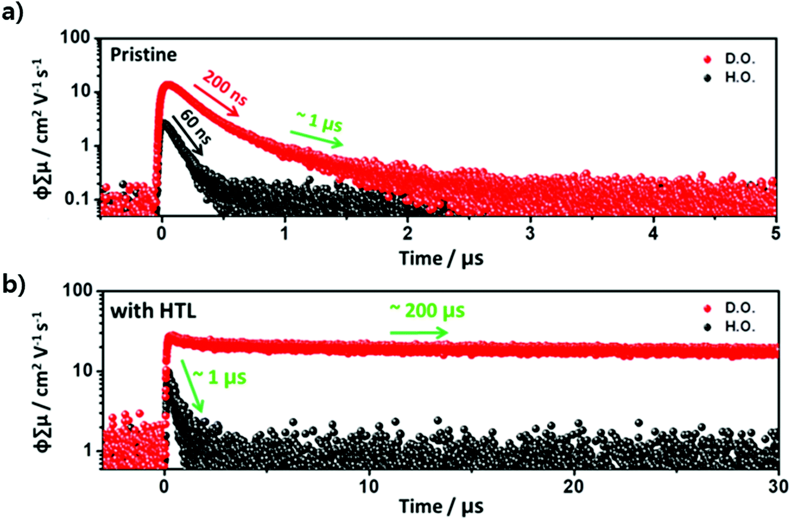
To provide further insight into the different behaviors of photo-induced charge carriers between H.O. and D.O. perovskites from the viewpoint of whole periodic dynamics, especially in the sub-micro and microsecond time region, FP-TRMC measurements were carried out. These experiments were conducted in an inert environment using 532 nm as the excitation source for the four samples, i.e., pristine perovskites H.O. and D.O. and layered H.O./HTL and D.O./HTL on a quartz plate.13 The advantage of the combination of TCSPC and FP-TRMC is that the rates of radiative and non-radiative recombination and the amplitudes of free charge carriers can be fully tracked as time evolves complementarily (Fig. 3). FP-TRMC traces recorded at different incident light intensities are shown in Fig. S4 (ESI†). Excitation intensity (photons cm−2) was adjusted from 1 × 10¹¹ to 2 × 10¹². As the excitation intensity decreased to 4 × 10¹¹, the highest Φ∑μ was observed, which originates from the formation of excess mobile charge carriers. Therefore, we conducted the FP-TRMC experiments for all the samples at an excitation intensity of 4 × 1011 cm−2, where the free charge carriers are maximally generated. The observed photoconductivity transients are shown in Fig. 3. The vertical axis Φ∑μ represents the product of the photo-generation efficiency of the free charge carriers (Φ) and the sum of the mobility of the hole and electron (∑μ = μh + μe). It can be assumed that all absorbed photons lead to the formation of free charge carriers at room temperature due to their relatively low binding energies in perovskite materials.25,26 D.O. perovskite showed photoconductivity (Φ∑μ = 13.7 cm2 V−1 s−1) with double exponential decay with time constants of 200 ns and 1 μs, while H.O. perovskite gave more than 5 times lower photoconductivity measured to be 2.6 cm2 V−1 s−1 with monoexponential decay with a time constant of 60 ns (Fig. 3a). The short time components (60 and 200 ns) of H.O. and D.O. correspond to the radiative recombination times observed in the TCSPC experiments. In H.O. perovskite, most of the free charge carriers are eliminated via the radiative recombination process. However, D.O. perovskite has long-lived charge carriers that are substantially maintained beyond a few microseconds. Free charge carriers can spread over a wide area in the D.O. perovskite owing to the diverse orientation structures, resulting in reduced probabilities of both radiative and non-radiative recombination. This is the main cause of the long-time component (1 μs). Because free charge carriers that dissipate rapidly have a negative effect on device performance, it is important to maximize the quantity of long-lived photo-induced charge carriers. Increasing the lattice orientation of perovskite materials can achieve this. In the FP-TRMC experiment of H.O. and D.O. perovskites in which the transporting layers were laid, surprisingly, a more pronounced effect was observed on the behavior of mobile free charge carriers (Fig. 3b). D.O./HTL showed a significantly increased photoconductivity (27.9 cm2 V−1 s−1) with a time component of hundreds of microseconds, whereas H.O./HTL exhibited a relatively low photoconductivity (9.8 cm2 V−1 s−1) with a monoexponential decay with a time constant of 1 μs. In summary, (i) the slower recombination rates seen in both D.O./HTL and H.O./HTL are affected by the hole extraction into the HTL, which inhibits unwanted recombination of mobile charge carriers with regard to the perovskite solar cell, (ii) the effect of layered HTL is more pronounced in D.O. than in H.O., which indicates enhanced mobility of photo-induced charge carriers and remarkably reduced probability of rapid charge recombination within the perovskite layer resulting from structural diversity. The spectroscopic interpretation of these results is presented in Fig. S5 (ESI†).
 |
| | Fig. 3 (a) Kinetic traces of photoconductivity transients of pristine perovskites of D.O. and H.O. recorded by FP-TRMC measurements. (b) Significantly changed kinetic traces when the hole transporting layer (HTL) was laid on D.O. and H.O. The excitation wavelength for the FP-TRMC measurements was 532 nm. | |
Perovskite solar cell devices
To link the effectiveness of the whole periodic photo-induced charge carrier dynamics to the photovoltaic performances, we fabricated PSCs with a planar architecture of glass/FTO/c-TiO2/meso-TiO2/perovskite/spiro-OMeTAD/Au, as shown in Fig. 4a. TiO2 and spiro-OMeTAD were used as the electron transporting layer (ETL) and HTL, respectively. To investigate the effect of the perovskite active layers, we used well-known transporting materials without special treatment.27–31 As shown in Fig. 4b, at a scan rate of 0.1 V s−1 with an aperture area of 0.09 cm2, the D.O. perovskite-based devices achieved an average PCE of 17.4% and a maximum PCE of 18.8%, whereas the H.O. perovskite-based devices showed average and maximum PCEs of 14.1% and 16.1%, respectively. The photovoltaic metrics of the PSCs (Fig. S6, ESI†) show higher average PCE values for the D.O. perovskite-based solar cells compared to those of the H.O. perovskite-based solar cells. The significant improvement in JSC and FF seems to be mainly due to the low density of recombination centers and higher absorbance. In Fig. S7 (ESI†), the external quantum efficiency (EQE) was measured to ensure the validity of the solar cell efficiency. These measurements agree with the results of spectroscopic experiments. This performance enhancement could be mainly due to (i) the increased mobility of photo-induced charge carriers, (ii) the reduced unwanted charge carrier recombination in the active layer, and (iii) the improved charge extraction from the active layer to the electrodes. Furthermore, the increased structural orientation could aid in efficient wide bandgap layer passivation on the active layer. Typically, efficiently passivated perovskite exhibits an improved PL lifetime owing to alleviated trap density.32 In the case of H.O. perovskite, however, the opposite result is most likely due to structural limitations of growth only in a specific direction (Fig. S8a, ESI†). However, D.O. perovskite which has various structural orientations and crystalline domain sizes seems to be well-passivated resulting in enhanced PL lifetime, as shown in Fig. S8b (ESI†). The D.O. perovskite showed remarkably improved PCE distribution (Fig. 4c), corresponding to this spectroscopic result.
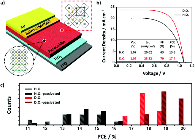 |
| | Fig. 4 (a) Simplified illustration of the perovskite solar cell device with the structure of glass/FTO/TiO2/perovskite/spiro-OMeTAD/Au. The black dashed circle and red dashed square represent the crystal structure of H.O. and D.O. perovskite, respectively. (b) J–V curves of the H.O. and D.O. perovskite-based solar cell devices, which show average efficiencies. (Inset shows detailed efficiency factors.) (c) Histograms of the J–V scan efficiencies of H.O. (dark grey), D.O. (red), passivated-H.O. (black), and passivated-D.O. (dark red) perovskite-based solar cells. | |
Conclusions
In summary, we combined TCSPC and FP-TRMC measurements to evaluate the whole periodic photo-induced charge carrier dynamics according to the orientation diversity of perovskites. Perovskites with various structural orientations showed a relatively long lifetime and improved mobility of free charge carriers, which is very important in that it enables an enhancement of device performance. As a result, perovskite with various structural orientations exhibited better power conversion efficiency than that of highly oriented perovskite. Although we have found a positive influence on the performance of PSCs by the diversity of structural orientation, further performance advancements can be derived through fine modulation of the crystal structure. Consequently, this study introduces a novel design for high-efficiency perovskite-based photovoltaic devices.
Author contributions
D. Kim and W. Cha conceived and designed this work. W. Cha performed the spectroscopic measurements and structural analysis. W. Cha, W.-Y. Cha and S. Seki performed the microwave conductivity measurements. W. Cha, I. Noh, and H. Ohkita fabricated the solar cell devices. W. Cha and W.-Y. Cha co-wrote the paper.
Conflicts of interest
There are no conflicts to declare.
Acknowledgements
This work at Yonsei University was supported by the National Research Foundation of Korea (NRF) grant funded by the Korean government (MSIT) (No. 2021R1A2C3006308). W.-Y. Cha acknowledges a JSPS Postdoctoral Fellowship for Research in Japan (P19345).
Notes and references
- A. Kojima, K. Teshima, Y. Shirai and T. Miyasaka, Organometal Halide Perovskites as Visible-Light Sensitizers for Photovoltaic Cells, J. Am. Chem. Soc., 2009, 131, 6050–6051 CrossRef CAS PubMed.
- M. M. Lee, J. Teuscher, T. Miyasaka, T. N. Murakami and H. J. Snaith, Efficient Hybrid Solar Cells Based on Meso-Superstructured Organometal Halide Perovskites, Science, 2012, 338, 643–647 CrossRef CAS PubMed.
- J. H. Heo, S. H. Im, J. H. Noh, T. N. Mandal, C.-S. Lim, J. A. Chang, Y. H. Lee, H.-J. Kim, A. Sarkar, M. K. Nazeeruddin, M. Grätzel and S. I. Seok, Efficient inorganic–organic hybrid heterojunction solar cells containing perovskite compound and polymeric hole conductors, Nat. Photonics, 2013, 7, 486–491 CrossRef CAS.
- M. A. Green, A. Ho-Baillie and H. J. Snaith, The emergence of perovskite solar cells, Nat. Photonics, 2014, 8, 506–514 CrossRef CAS.
- H. Zhou, Q. Chen, G. Li, S. Luo, T.-B. Song, H.-S. Duan, Z. Hong, J. You, Y. Liu and Y. Yang, Interface engineering of highly efficient perovskite solar cells, Science, 2014, 345, 542–546 CrossRef CAS PubMed.
- N. J. Jeon, J. H. Noh, W. S. Yang, Y. C. Kim, S. Ryu, J. Seo and S. I. Seok, Compositional engineering of perovskite materials for high-performance solar cells, Nature, 2015, 517, 476–480 CrossRef CAS PubMed.
- W. S. Yang, J. H. Noh, N. J. Jeon, Y. C. Kim, S. Ryu, J. Seo and S. I. Seok, High-performance photovoltaic perovskite layers fabricated through intramolecular exchange, Science, 2015, 348, 1234–1237 CrossRef CAS PubMed.
- K.-H. Jung, J.-Y. Seo, S. Lee, H. Shin and N.-G. Park, Solution-processed SnO2 thin film for a hysteresis-free planar perovskite solar cell with a power conversion efficiency of 19.2%, J. Mater. Chem. A, 2017, 5, 24790–24803 RSC.
- A.-N. Cho, I.-H. Jang, J.-Y. Seo and N.-G. Park, Dependence of hysteresis on the perovskite film thickness: inverse behavior between TiO2 and PCBM in a normal planar structure, J. Mater. Chem. A, 2018, 6, 18206–18215 RSC.
- J. Chen, S.-G. Kim, S. Ren, H. S. Jung and N.-G. Park, Effect of bidentate and tridentate additives on the photovoltaic performance and stability of perovskite solar cells, J. Mater. Chem. A, 2019, 7, 4977–4987 RSC.
- J. J. Yoo, G. Seo, M. R. Chua, T. G. Park, Y. Lu, F. Rotermund, Y.-K. Kim, C. S. Moon, N. J. Jeon, J.-P. Correa-Baena, V. Bulović, S. S. Shin, M. G. Bawendi and J. Seo, Efficient perovskite solar cells via improved carrier management, Nature, 2021, 590, 587–593 CrossRef CAS PubMed.
- J. Jeong, M. Kim, J. Seo, H. Lu, P. Ahlawat, A. Mishra, Y. Yang, M. A. Hope, F. T. Eickemeyer, M. Kim, Y. J. Yoon, I. W. Choi, B. P. Darwich, S. J. Choi, Y. Jo, J. H. Lee, B. Walker, S. M. Zakeeruddin, L. Emsley, U. Rothlisberger, A. Hagfeldt, D. S. Kim, M. Grätzel and J. Y. Kim, Pseudo-halide anion engineering for α-FAPbI3 perovskite solar cells, Nature, 2021, 592, 381–385 CrossRef CAS PubMed.
- E. Nakanishi, R. Nishikubo, A. Wakamiya and A. Saeki, How the Mixed Cations (Guanidium, Formamidinium,
and Phenylethylamine) in Tin Iodide Perovskites Affect Their Charge Carrier Dynamics and Solar Cell Characteristics, J. Phys. Chem. Lett., 2020, 11, 4043–4051 CrossRef CAS PubMed.
- E. M. Hutter and T. J. Savenije, Thermally Activated Second-Order Recombination Hints toward Indirect Recombination in Fully Inorganic CsPbI3 Perovskites, ACS Energy Lett., 2018, 3, 2068–2069 CrossRef CAS PubMed.
- T. J. Savenije, D. Guo, V. M. Caselli and E. M. Hutter, Quantifying Charge-Carrier Mobilities and Recombination Rates in Metal Halide Perovskites from Time-Resolved Microwave Photoconductivity Measurements, Adv. Energy Mater., 2020, 10, 1903788 CrossRef CAS.
- S. Zhang, S. Wu, R. Chen, W. Chen, Y. Huang, H. Zhu, Z. Yang and W. Chen, Controlling Orientation Diversity of Mixed Ion Perovskites: reduced Crystal Microstrain and Improved Structural Stability, J. Phys. Chem. Lett., 2019, 10, 2898–2903 CrossRef CAS PubMed.
- G. Zheng, C. Zhu, J. Ma, X. Zhang, G. Tang, R. Li, Y. Chen, L. Li, J. Hu, J. Hong, Q. Chen, X. Gao and H. Zhou, Manipulation of facet orientation in hybrid perovskite polycrystalline films by cation cascade, Nat. Commun., 2018, 9, 2793 CrossRef PubMed.
- Z. Xu, Z. Liu, N. Li, G. Tang, G. Zheng, C. Zhu, Y. Chen, L. Wang, Y. Huang, L. Li, N. Zhou, J. Hong, Q. Chen and H. Zhou, A Thermodynamically Favored Crystal Orientation in Mixed Formamidinium/Methylammonium Perovskite for Efficient Solar Cells, Adv. Mater., 2019, 31, 1900390 CrossRef PubMed.
- T. Baikie, Y. Fang, J. M. Kadro, M. Schreyer, F. Wei, S. G. Mhaisalkar, M. Grätzel and T. J. White, Synthesis and crystal chemistry of the hybrid perovskite (CH3NH3)PbI3 for solid-state sensitised solar cell applications, J. Mater. Chem. A, 2013, 1, 5628–5641 RSC.
- S. Prathapani, P. Bhargava and S. Mallick, Electronic band structure and carrier concentration of formamidinium–cesium mixed cation lead mixed halide hybrid perovskites, Appl. Phys. Lett., 2018, 112, 092104 CrossRef.
- Y. Xue, J. Tian, H. Wang, H. Xie, S. Zhu, B. Zheng, C. Gaob and X. Liu, Localized incorporation of cesium ions to improve formamidinium lead iodide layers in perovskite solar cells, RSC Adv., 2018, 8, 25645–25652 RSC.
- A. Maqsood, Y. Li, J. Meng, D. Song, B. Qiao, S. Zhao and Z. Xu, Perovskite Solar Cells Based on Compact, Smooth FA0.1MA0.9PbI3 Film with Efficiency Exceeding 22%, Nanoscale Res. Lett., 2020, 15, 89 CrossRef CAS PubMed.
- A. E. Shalan, T. Oshikiri, S. Narra, M. M. Elshanawany, K. Ueno, H.-P. Wu, K. Nakamura, X. Shi, E. W.-G. Diau and H. Misawa, Cobalt Oxide (CoOx) as an Efficient Hole-Extracting Layer for High-Performance Inverted Planar Perovskite Solar Cells, ACS Appl. Mater. Interfaces, 2016, 8, 33592–33600 CrossRef CAS PubMed.
- Q.-D. Yang, J. Li, Y. Cheng, H.-W. Li, Z. Guan, B. Yu and S.-W. Tsang, Graphene oxide as an efficient hole-transporting material for high-performance perovskite solar cells with enhanced stability, J. Mater. Chem. A, 2017, 5, 9852–9858 RSC.
- Z. Yang, A. Surrente, K. Galkowski, A. Miyata, O. Portugall, R. J. Sutton, A. A. Haghighirad, H. J. Snaith, D. K. Maude, P. Plochocka and R. J. Nicholas, Impact of the Halide Cage on the Electronic Properties of Fully Inorganic Cesium Lead Halide Perovskites, ACS Energy Lett., 2017, 2, 1621–1627 CrossRef CAS.
- M. C. Gélvez-Rueda, D. H. Cao, S. Patwardhan, N. Renaud, C. C. Stoumpos, G. C. Schatz, J. T. Hupp, O. K. Farha, T. J. Savenije, M. G. Kanatzidis and F. C. Grozema, Effect of Cation Rotation on Charge Dynamics in Hybrid Lead Halide Perovskites, J. Phys. Chem. C, 2016, 120, 16577–16585 CrossRef.
- C.-Y. Chang, H.-H. Huang, H. Tsai, S.-L. Lin, P.-H. Liu, W. Chen, F.-C. Hsu, W. Nie, Y.-F. Chen and L. Wang, Facile Fabrication of Self-Assembly Functionalized Polythiophene Hole Transporting Layer for High Performance Perovskite Solar Cells, Adv. Sci., 2021, 8, 2002718 CrossRef CAS PubMed.
- F. Juan, Y. Wu, B. Shi, M. Wang, F. Xu, J. Jia, H. Wei, T. Yang and B. Cao, Plasmonic Au Nanooctahedrons Enhance Light Harvesting and Photocarrier Extraction in Perovskite Solar Cell, ACS Appl. Energy Mater., 2021, 4, 3201–3209 CrossRef CAS.
- J. Ma, J. Chang, Z. Lin, X. Gua, L. Zhou, H. Xi, D. Chen, C. Zhang and Y. Hao, Elucidating the Roles of TiCl4 and PCBM Fullerene Treatment on TiO2 Electron Transporting Layer for Highly Efficient Planar Perovskite Solar Cells, J. Phys. Chem. C, 2018, 122, 1044–1053 CrossRef CAS.
- A. Agresti, S. Pescetelli, L. Cinà, D. Konios, G. Kakavelakis, E. Kymakis and A. D. Carlo, Efficiency and Stability Enhancement in Perovskite Solar Cells by Inserting Lithium-Neutralized Graphene Oxide as Electron Transporting Layer, Adv. Funct. Mater., 2016, 26, 2686–2694 CrossRef CAS.
- J. Liu, X. Yin, Y. Gua, M. Que, J. Chen, Z. Chen and W. Que, Influence of Hole Transport Layers/Perovskite Interfaces on the Hysteresis Behavior of Inverted Perovskite Solar Cells, ACS Appl. Energy Mater., 2020, 3, 6391–6399 CrossRef CAS.
- D. Kim, H. J. Jung, I. J. Park, B. W. Larson, S. P. Dunfield, C. Xiao, J. Kim, J. Tong, P. Boonmongkolras, S. G. Ji, F. Zhang, S. R. Pae, M. Kim, S. B. Kang, V. Dravid, J. J. Berry, J. Y. Kim, K. Zhu, D. H. Kim and H. Shin, Efficient, stable silicon tandem cells enabled by anion-engineered wide-bandgap perovskites, Science, 2020, 368, 155–160 CrossRef CAS PubMed.
Footnotes |
| † Electronic supplementary information (ESI) available: Details of structural analysis, photophysical properties, and device performance. See DOI: 10.1039/d1qm01586a |
| ‡ Both authors contributed equally to this manuscript. |
|
| This journal is © the Partner Organisations 2022 |

 c,
Shu
Seki
c,
Shu
Seki