
 Open Access Article
 This Open Access Article is licensed under a
 Creative Commons Attribution 3.0 Unported Licence
Thermal atomic layer deposition of In2O3 thin films using a homoleptic indium triazenide precursor and water
Pamburayi
Mpofu
 ,
Polla
Rouf
,
Nathan J.
O'Brien
,
Urban
Forsberg
and
Henrik
Pedersen
*
,
Polla
Rouf
,
Nathan J.
O'Brien
,
Urban
Forsberg
and
Henrik
Pedersen
*
Department of Physics, Chemistry and Biology, Linköping University, SE-581 83 Linköping, Sweden. E-mail: henrik.pedersen@liu.se
First published on 22nd February 2022
Abstract
Indium oxide (In2O3) is an important transparent conducting material widely used in optoelectronic applications. Herein, we study the deposition of In2O3 by thermal atomic layer deposition (ALD) using our recently reported indium(III) triazenide precursor and H2O. A temperature interval with self-limiting growth was found between ∼270 and 385 °C with a growth per cycle of ∼1.0 Å. The deposited films were polycrystalline cubic In2O3 with In![[thin space (1/6-em)]](https://www.rsc.org/images/entities/char_2009.gif) :O ratios of 1:1.2, and low levels of C and no detectable N impurities. The transmittance of the films was found to be >70% in visible light and the resistivity was found to be 0.2 mΩ cm. The high growth rates, low impurities, high optical transmittance, and low resistivity of these films give promise to this process being used for ALD of In2O3 films for future microelectronic displays.
:O ratios of 1:1.2, and low levels of C and no detectable N impurities. The transmittance of the films was found to be >70% in visible light and the resistivity was found to be 0.2 mΩ cm. The high growth rates, low impurities, high optical transmittance, and low resistivity of these films give promise to this process being used for ALD of In2O3 films for future microelectronic displays.
I. Introduction
Indium oxide (In2O3) is a material of high interest due to its high electrical conductivity and optical transparency, making it a key material for transparent and optoelectronics1e.g. microelectronic displays on touch screens. The electrical conductivity of In2O3 is controlled by the stoichiometry of the film2,3 and is typically enhanced by substituting the In atoms with 5–10 atomic % Sn.4,5 All applications of In2O3 as transparent conducting layers require the deposition of high-quality thin films of In2O3. This requirement is the driving force for extensive studies by sputtering,6 thermal evaporation,7 chemical vapor deposition,8 and atomic layer deposition (ALD).9 ALD of In2O3 is especially interesting as it can deposit high quality films with precise thickness, controlled composition, low impurity contents, and excellent conformality on complex substrates.10ALD of In2O3 was first reported using InCl3 and either H2O or H2O2 at temperatures between 300–500 °C.11 The low vapor pressure of InCl3, the generation of HCl as the reaction by-product and the possibility for InCl3 to etch the growing In2O3 layer12 has motivated the use of other In precursors. Furthermore, there has been limitations on availability of efficient In precursors that give processes with high growth rates, fully self-limiting reactions, low impurity contents and good film crystallinity. The In compounds tested as precursors in combination with different reactants, within different deposition temperature windows are shown in Table 1.
| Indium precursor | Reactant | Temperature window (°C) | Ref. |
|---|---|---|---|
| Cp = cyclopentadienyl, acac = acetylacetonate, tmhd = 2,2,6,6-tetramethyl-3,5-heptanedionate, guan = N,N-dimethyl-N′,N′′-diisopropylguanidinato, famd = N,N′-diisopropylformamidinato, amd = N,N′-diisopropylamidinato, DAT = dimethylbutylamino-trimethyl, TMS = trimethylsilyl, NCA = diethyl[1,1,1-trimethyl-N-(trimethylsilyl)silanaminato], DAD = [3-(dimethylamino)propyl]dimethyl, dmamp = 1-dimethylamino-2-methyl-2-propoxy, EDPA = N-ethoxy-2,2-dimethylpropanamido. | |||
| InCl3 | H2O/H2O2 | 300–500 | 11, 13 and 14 |
| InMe3 | H2O | 200–250 | 15 and 16 |
| InMe3 | O3 | 100–200 | 17 |
| InCp | O3 | 200–450 | 12 |
| InCp | H2O/O2 | 100–350 | 18–21 |
| InCp | H2O2 | 160–200 | 10 and 22 |
| In(acac)3 | H2O or O3 | 165–220 (H2O), 160–225 (O3) | 23 |
| In(tmhd)3 | O2 plasma | 100–400 | 24 |
| In(guan)3 | H2O | 230–300 | 25 |
| Et2InN(TMS)2 | H2O | 175–250 | 26 |
| InNCA, DADIn, InEt3 | O3 | 100–200 | 27 |
| InNCA | H2O2 | 125–225 | 28 |
| In(dmamp)3 | O3 | 100–300 | 29 |
| Me2In(EDPA) | O2 plasma | 70–250 | 30 |
| In(famd)3 and In(amd)3 | H2O | 150–275 and 225–300 | 31 |
| In(CH3)3[CH3OCH2CH2NHtBu] | H2O | 150–200 | 32 |
| DATIn | O2 plasma | 100–200 | 33 |
| InCp | O2 plasma | 225–275 | 34 |
Amidinate and guanidinate ligands have been employed to improve the thermal stability of In precursors whilst maintaining sufficient reactivity for surface reactions. This has led to the formation of homoleptic hexacoordinated In–N bonded precursors, In(III) tris-formamidinate31 (In(famd)3) 1, amidinate35 (In(amd)3) 2 and guanidinate36 (In(guan)3,) 3 (Fig. 1a). As the coordination sphere of the metal centre is all In–N bonds, their use for In2O3 is especially attractive as it makes formation of In–O bonds thermodynamically favourable. This would allow H2O to be used as the co-reactant and remove the need for strong reactants such as O3 and O2 plasma. Precursors 1–3 have been used with H2O for thermal ALD of In2O3 with all showing self-limiting growth behaviour.25,31 Although all precursors gave similar growth rates of In2O3 (0.45–0.55 Å per cycle), 1 was found to have faster kinetics with the surface and H2O than 2 and 3. A surface chemical model was used to explain the faster kinetics of 1, which was thought to be due to its smaller endocyclic carbon substituent. This allowed the exocyclic N-isopropyl groups of the ligand to fold up more, leading to a surface species with less surface repulsion and a more exposed In centre for its subsequent reaction with H2O.31 This surface chemical model was further confirmed when we used 1–3 for plasma ALD of InN.37 Again, 1 was found to be superior to 2 and 3. To continue this trend, we replaced the substituted endocyclic carbon to a nitrogen atom. This led to our discovery of the indium(III) triazenide (4) (Fig. 1b), which we used with NH3 plasma to render high-quality InN.38
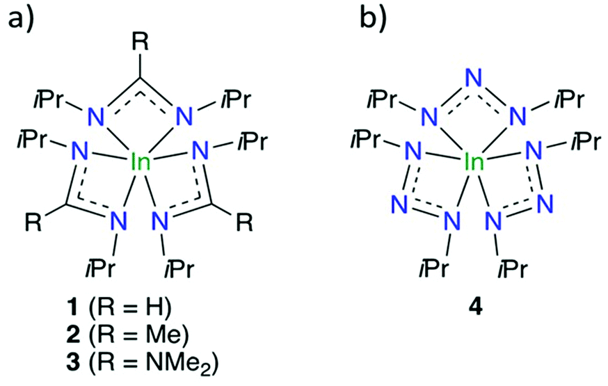 | ||
| Fig. 1 (a) Evolution of In(III) precursors 1–3, used in various indium-based ALD studies, and (b) 4. | ||
Here, we investigate the use of 4 as In precursor in thermal ALD of In2O3 with H2O as reactant. The ALD characteristics, optical and electrical properties of the deposited In2O3 films are investigated and a direct comparison between 4 and 1 is undertaken.
II. Experimental
A. Film deposition
Precursors 1 and 4 were synthesised using literature procedures.37,38 Films were deposited using a homebuilt crossflow ALD reactor at 50 hPa. A flow of N2 (99.999%) was used as the carrier and purging gas. At all times during the deposition, the N2 pressure was kept constant. Precursor 1 or 4 and H2O were used as the In and O sources, respectively. The precursors were introduced separately into the reactor via stainless steel gas lines, which were extended into the reactor tube to ensure maximum substrate exposure. Precursors 1 and 4 were placed in a stainless-steel bubbler, which was heated to 120 °C, the gas delivery line was heated to 140 °C and flow of precursor into the chamber was aided by N2 carrier gas. The deionized H2O was kept at room temperature and delivered into the chamber without a carrier gas. Film deposition was undertaken on approximately 2 × 3 cm Si (100) and glass substrates, which were cleaned by dry N2 gas and used without further chemical cleaning. After loading the substrates, the chamber was baked at 155 °C overnight. The deposition zone of the reactor was defined by the heated zone of the tube furnace. Unless otherwise noted, a typical ALD cycle consisted of a 4 s pulse of 1 or 4 and 3 s pulse of H2O, with 10 s N2 purges after the In precursor and the water pulses. The deposition process was studied between 150 and 520 °C.B. Film characterization
The crystallographic phases of the films were characterized by a X-ray diffractometer (XRD) PANalytical X'pert Pro equipped with a Cu Kα X-ray source (λ = 1.54 Å) in the θ–2θ mode. A Ni foil was used to filter the Kβ radiation. Film thickness was measured using the same PANalytical X'Pert Pro X-ray diffractometer in X-ray reflectivity (XRR) mode. The film thickness was obtained from the XRR data using X'Pert reflectivity software and a two-layer model, In2O3/Si, to fit the data. The film morphology was analyzed by scanning electron microscopy (SEM) using a LEO 1550 scanning electron microscope with an acceleration energy of 2 kV using the in-lens detector at a working distance of 3–6 mm. SEM was also used to obtain film thickness on samples that were too thick or rough for XRR measurements. The composition and impurity levels of the deposited films were probed with high resolution X-ray photoelectron spectroscopy (XPS), Kratos AXIS Ultra DLD, equipped with an Ar (0.30 eV) sputtering source for 600 s, employing monochromatic Al Kα radiation (hν = 1486.6 eV). Sputter-cleaning (sputter-etching) was undertaken to eliminate surface contamination, which resulted after exposure of the substrate to air. Analysis of the photoelectron spectra was completed using the CasaXPS software package. By quantitative analysis, the signals originating from the substrate and the thin film could be de-convoluted and the chemical composition was obtained. Gaussian-Laurentius functions and Shirley background were used to fit the experimental XPS data.The optical, transmittance, absorbance, and bandgap properties of the films were obtained using a Shimadzu UV-2450 UV-VIS spectrophotometer in a wavelength range of 250–800 nm. The UV-VIS spectrophotometer was operated in the reflectance mode in analyzing films deposited on glass substrates. Determination of band gap was determined using the Tauc plot formalism from data obtained by UV-Vis spectrophotometry based on the Tauc relation: (αhν)1/y = β(hν − Eg) where α is the absorption coefficient (absorbance/film thickness), β is the band tailing parameter, h is the Planck's constant, ν is the frequency of incident light, Eg is the energy of the optical band gap and y is the power factor, which depends upon the nature of the transition (semi-conducting materials, y = 0.5 for direct allowed transitions). Therefore: (αhν)2 = β(hν − Eg).
By drawing a tangential line from the plotted graph of hν versus (αhν)2, the value of the band gap was determined as the value of hν at the point where this line crosses the axis i.e. the intercept of the extrapolation to near zero absorption with photon energy axis i.e. (αhν)2 → 0. Electrical characterization by resistivity measurements were performed using the 4-point probe technique. Measurements were done on a Jandel, Model RM3000 test unit or probing system, which was first calibrated using a standard glass sample before sample resistivities were determined.
III. Results and discussion
A. Film deposition
The ALD process with 4 and H2O was studied by varying their pulse lengths at 290 °C. The resulting saturation curves (Fig. 2a) show the deposition process is self-limiting for pulse times ≥3 s, resulting in film growth of ∼1.0 Å per cycle. Varying the deposition temperature whilst using a 4 s pulse of 4 and 3 s pulse of H2O revealed a temperature interval where the growth per cycle (GPC) is constant with the temperature between 270 and 385 °C (Fig. 2b). The film thickness at 290 °C using 300, 500, 800 and 1100 ALD cycles (Fig. 2c) follows a linear trend line, however, it shows a significantly slower initial deposition interpreted as a nucleation delay of approximately 49 cycles. This result suggests slow surface kinetics of 4 at low temperatures presumably due to steric crowding of the metal centre. Similar behaviour was also reported for ALD of InN from 1, whereby multiple pulses of 1 was used to circumvent this problem.37 Attempts to fit a linear trend line results in an average growth per cycle of 0.9 Å.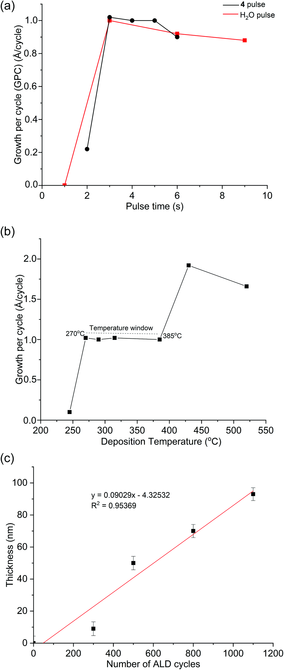 | ||
| Fig. 2 (a) Growth per cycle behaviour of 4 and H2O pulses at 290 °C on Si (100). (b) Growth dependence on process temperature using a 4 s pulse of 4 and 3 s pulse of H2O on Si(100). (c) Growth behaviour of 4 at 290 °C dependent on the number of cycles using a 4 s pulse of 4 and 3 s pulse of H2O on Si(100). | ||
B. Film properties
The θ–2θ XRD analysis of films deposited at 315 °C and 430 °C (Fig. 3) showed cubic In2O3 as the only crystalline phase except the Si substrate. In addition, the films are polycrystalline with a preferred (222) orientation.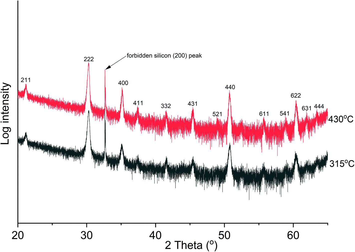 | ||
| Fig. 3 The θ–2θ XRD analysis of deposited films at 315 °C (50 nm thick) and 430 °C (96 nm thick), showing polycrystalline cubic In2O3 films. | ||
XPS analysis of the films showed the C impurities range from 0.8 to 3.5 at% and N impurities are below the detection limit. As summarized in Table 2, XPS analysis also shows the films are oxygen deficient, which is comparable to literature.10 The elemental composition of the films displayed in Table 2 indicates that higher deposition temperatures and H2O pulse times lower the impurity concentrations. A longer H2O pulse also increases the O content and reduces the impurity content of the films. The oxygen deficient nature of the deposited films opens the possibility of O vacancies in the In2O3 films. Oxygen vacancies are point defects39 critical for explaining the optoelectrical properties of metal oxide thin films.40
| Deposition temperature (°C) | C (at%) | In (at%) | O (at%) | Atomic ratio In:O (expected 1:1.5) |
|---|---|---|---|---|
| 290 | 3.5 | 43.5 | 53.0 | 1:1.2 |
| 315 | 1.4 | 45.0 | 53.6 | 1:1.2 |
| 385 | 0 | 51.5 | 48.5 | 1:0.9 |
| Water pulse length (s) | ||||
| 3 | 4.3 | 43.2 | 52.5 | 1:1.2 |
| 6 | 1.3 | 45.3 | 53.4 | 1:1.2 |
| 9 | 0.8 | 45.6 | 53.6 | 1:1.2 |
| 12 | 1.3 | 44.7 | 54.0 | 1:1.2 |
Top view SEM images of 50 nm and 96 nm thick films deposited at 290 °C and 430 °C respectively (Fig. 4) showed smooth films at lower temperatures (Fig. 4a), and larger, flattened, and faceted grains at higher temperatures (Fig. 4b). Cross-section micrographs further indicated smooth and uniform films grown at 315 °C (Fig. 4c).
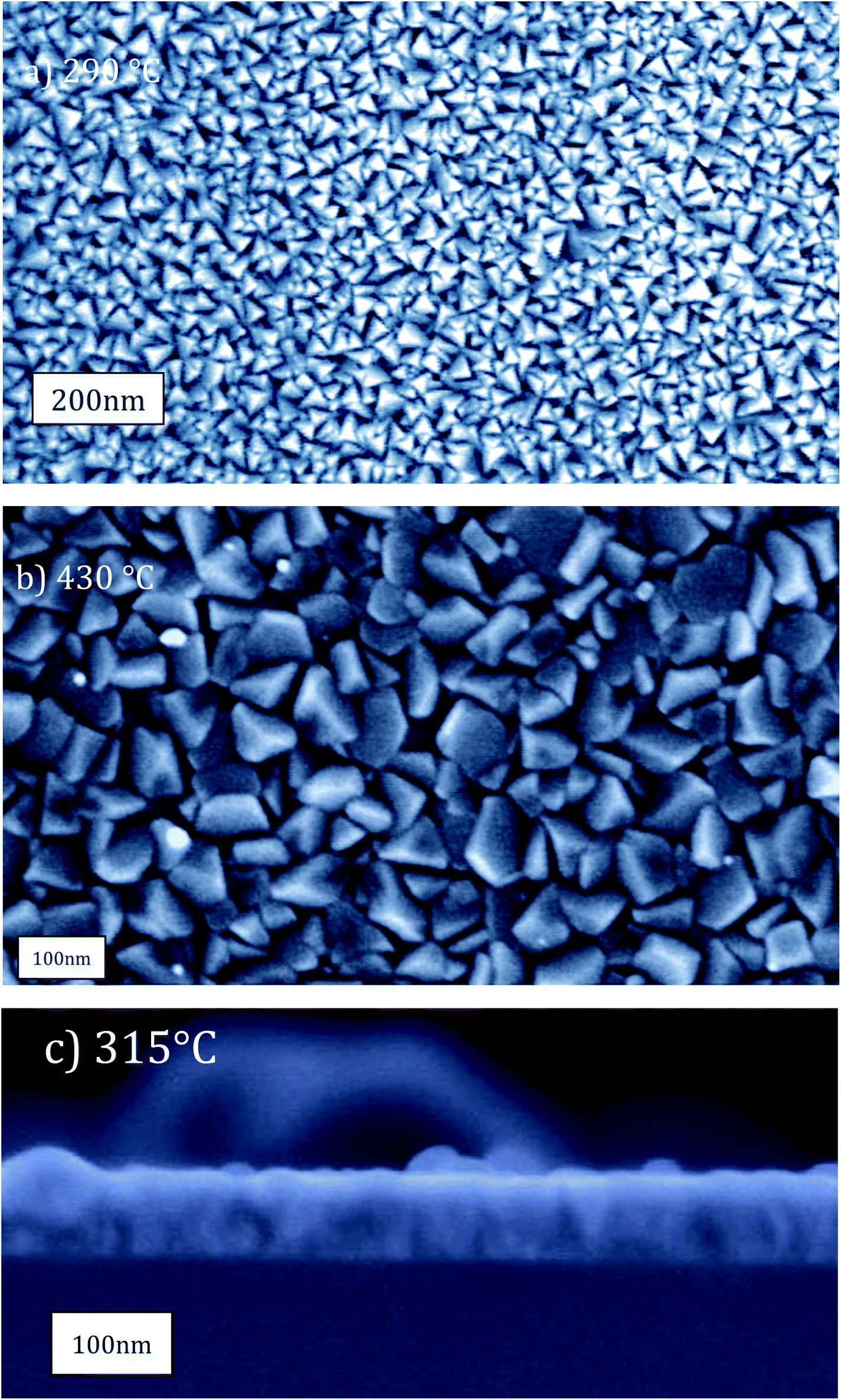 | ||
| Fig. 4 SEM micrographs for films deposited at (a) 290 °C, (b) 430 °C and at (c) 315 °C. | ||
The results above show In2O3 can be deposited from 4 and H2O in an ALD process. We speculate that the primary reaction mechanism for the film deposition is a surface chemical reaction of ligand exchange type, similar to what has been suggested for ALD of In2O3 from 1 and water.31 Presumably, 4 loses one or two triazenide ligands upon chemisorption by reacting with surface hydroxyl groups, forming In–O bonds and protonated triazenide ligands. A similar ligand exchange takes place during the water pulse to remove the remaining surface triazenide ligands and replacing them with new hydroxyl groups.
The resistivity of approximately 50 nm In2O3 films deposited on glass at 290 °C with different H2O pulse lengths was determined by four-point probe measurements. The film resistivity reflects the electrical properties of a film since it is determined by the carrier concentration and carrier mobility. Electrical conductivity of In2O3 is reported to be mainly controlled by the oxygen stoichiometry of the film.41 A perfect In2O3 stoichiometry is not ideal since it has no oxygen vacancies, which results in increased resistivity.42 In2O3 typically exhibits n-type semiconducting properties from the oxygen vacancies,19 which increase carrier density and hence act as donors.1 The deposited films in this study show a general decrease in resistivity, i.e., an increase in conductivity, with longer H2O pulse time. The improved conductivity for films deposited with increased H2O dosage may be attributed to incorporation of hydroxyl groups which cause self-doping.43 The resistivities of different film samples, all with approximately 50 nm thicknesses, deposited with 6 s, 9 s and 12 s of H2O pulse were 1.2; 2.6 and 0.16 mΩ cm, respectively (Table 3). Upon postdeposition annealing at 520 °C for 2 hours in air, the In:O ratio in the film changed from 1:1.2 to 1:1.3 but this lead to an increase in the resistivity from e.g., 1.2 to 2.0 mΩ cm (shown in Table 3). This result is in line with previous reports on the importance of the oxygen vacancies for the electrical conductivity of the In2O3 films.
| H2O pulse (s) | Average sheet resistance as deposited (ohms per square) | Resistivity (mΩ cm) | H2O pulse (s) | Average sheet resistance after post-annealing at 520 °C (ohms per square) | Resistivity (mΩ cm) |
|---|---|---|---|---|---|
| 6 | 238.8 | 1.2 | 6 | 400.6 | 2.0 |
| 9 | 506.8 | 2.6 | 9 | 1500.0 | 7.5 |
| 12 | 32.2 | 0.16 | 12 | 40.4 | 0.2 |
Optical transparency of the films was obtained from the transmission spectrum of 50 nm thick In2O3 films deposited at 290 °C on glass referenced to the spectrum of the uncoated glass substrate. The resultant average transmission of the In2O3 film in the wavelength range 250–800 nm was calculated using the relationship A = 2 − log10(%T), where A is absorbance and T is transmittance of light. The spectra in Fig. 5 shows the optical transmittance for the In2O3 films with uncoated glass included for reference. The highest obtained optical transmittance was 71%, which is very similar to an uncoated glass substrate, which showed 74% transmittance. The optical transmittance of the In2O3 films is comparable to values already reported in literature.23,44 With uncoated glass being the control, it would be 71/74 × 100% which equals 96% transmittance in relation to glass. Fig. 5 shows that the transmittance increases with longer water pulse, which from Table 2, renders higher oxygen content in the film.
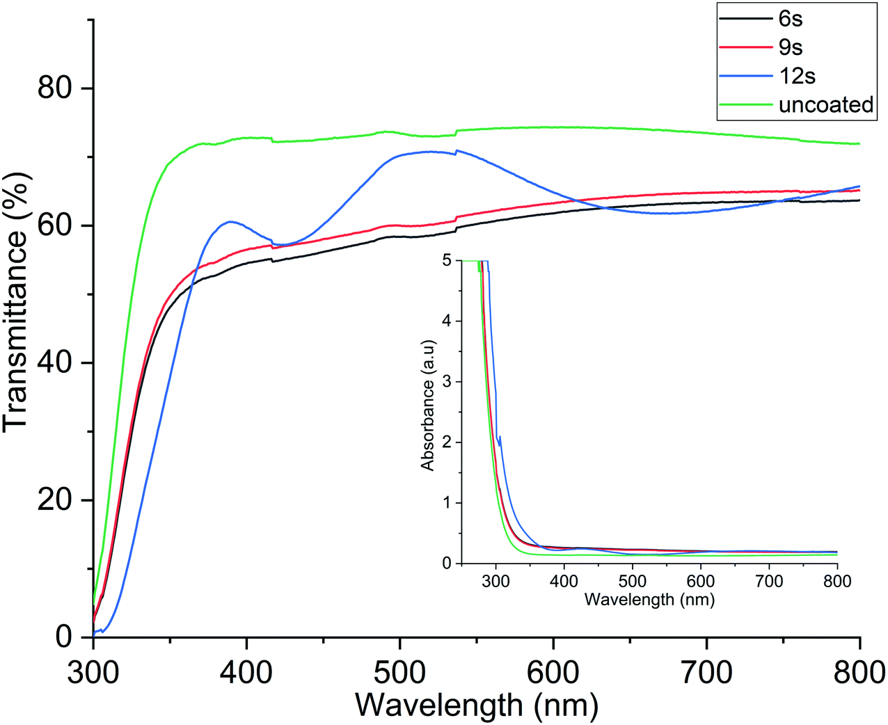 | ||
| Fig. 5 Optical transmittance of the In2O3 films deposited with different lengths of the H2O pulse. The transmittance increases with increasing H2O pulse time. | ||
The results from the resistivity and transmittance measurements are in line with the literature on In2O3 where the oxygen stoichiometry in the films which has been shown to impact both optical transmission and electrical conductivity of the films.19 The high concentration of oxygen vacancies causes our films to be more conducting than those reported in previous studies.41,45
Tauc plots of the In2O3 films deposited with different H2O pulse lengths are shown in Fig. 6, indicating that the direct optical band gap varies between 4.0 and 4.2 eV with higher band gap for shorter H2O pulses. The bandgap is lower for higher oxygen content in the films. The obtained band gap (4.0–4.2 eV) is comparable to previously reported values but is slightly higher than the expected range (3.5–3.9 eV). The higher band gap is ascribed to the deposition temperatures used in our study, which are higher than what is typically employed in ALD of In2O3. From our XPS results (Table 2), higher deposition temperatures render lower oxygen content and carbon incorporation in the films. We speculate that this leads to an increase of oxygen vacancies41 that can supply free electrons42 in the material leading to an increase in the optical band gap. A higher temperature can also increase the optical band gap by decreasing the density of grain boundaries, leading to fewer electrons being trapped in grain boundaries, increasing the number of free electrons.46 This increase of band gap can be further explained by the gap widening phenomenon called the Burstein–Moss shift.47
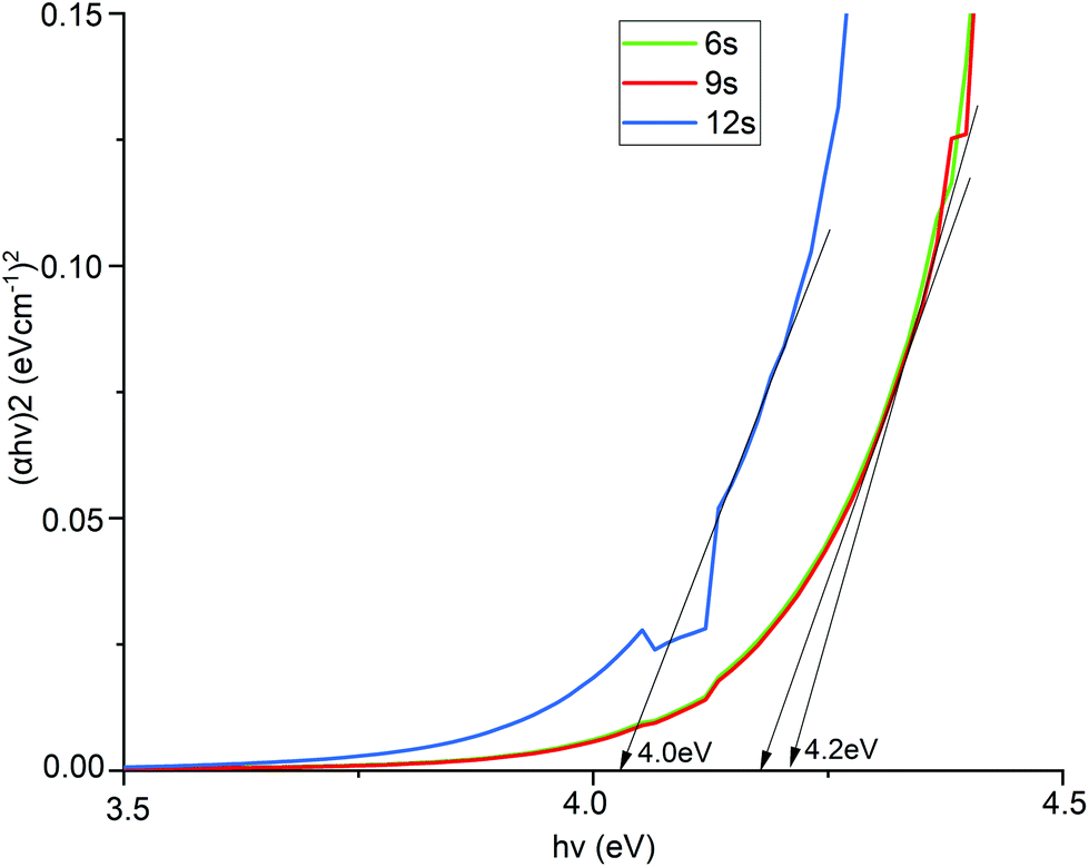 | ||
| Fig. 6 Tauc plots for estimating the optical band gaps of In2O3 films deposited with different H2O pulse times. | ||
C. Comparison to the In(famd)3 precursor (1)
ALD using 4 and H2O renders In2O3 films with properties comparable to previous studies using 1, albeit 4 seems to require higher deposition temperatures. A temperature window of 150–275 °C for In2O3 films using 1 and H2O was reported, but slow surface kinetics of 1 were observed.31 This was then circumvented using a stop-flow process to give 1 more time to react with the surface. We could not utilize a stop-flow process in our ALD reactor, therefore undertook a direct comparison between 1 and 4 by studying 1 and H2O in our reactor. We found a temperature interval of 245–315 °C where the GPC is constant with the temperature when using a 5 s pulse of 1 and 4 s pulse of H2O (Fig. 7). This is higher than the 150–275 °C reported for 1, again showing its slow surface kinetics.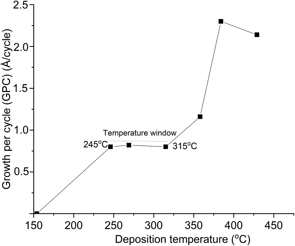 | ||
| Fig. 7 Growth per cycle vs. deposition temperature for ALD of In2O3 using 1 and H2O in our ALD reactor, which does not have stop flow mode. | ||
A stop flow mode was used to allow for a lower deposition temperature of In2O3 using 1, whilst we employed a multiple-pulse approach using 1 for depositing InN by ALD.37 The higher temperature interval found for ALD of In2O3 using 1 in our ALD reactor suggest that the temperature window obtained for 4 could possibly also be lowered by using stop flow mode. What perhaps speaks against this is that ALD of InN using 4 did not require the multiple pulse approach used for ALD of InN using 1.
IV. Summary and conclusions
In summary, we used our recently reported In(III) triazenide precursor in combination with H2O to deposit In2O3 films in a thermal ALD process. Polycrystalline In2O3 films with a cubic structure were successfully deposited. The GPC, impurities, and In/O ratios are in line with the literature for other In precursors. The transmittance was found to be >70% in visible light and the resistivity was found to be 0.2 mΩ cm. A temperature interval with self-limiting growth was found between 270–385 °C. This is higher than that for ALD of In2O3 using the previously reported 1. After a direct comparison between the two In precursors used in this study, we suggest the temperature interval for 4 could be lowered by using a stop flow mode ALD process.Conflicts of interest
There are no conflicts to declare.Acknowledgements
This work was financially supported by the Swedish Foundation for Strategic Research through the project “Time-resolved low temperature CVD for III-nitrides” (no. SSF-RMA 15-0018). PM acknowledges the Swedish Institute for funding his master program studies at Linköping University.Notes and references
- O. Bierwagen, Semicond. Sci. Technol., 2015, 30, 24001 CrossRef CAS.
- M. F. Bhopal, D. won Lee, A. Rehman and S. H. Lee, Vacuum, 2016, 133, 108–113 CrossRef CAS.
- N. Balasubramanian and A. Subrahmanyam, J. Phys. D: Appl. Phys., 1989, 22, 206–209 CrossRef CAS.
- H. Kim, C. M. Gilmore, A. Piqué, J. S. Horwitz, H. Mattoussi, H. Murata, Z. H. Kafafi and D. B. Chrisey, J. Appl. Phys., 1999, 86, 6451–6461 CrossRef CAS.
- M. Mazur, D. Kaczmarek, J. Domaradzki, D. Wojcieszak, S. Song and F. Placido, Conf. Proc. - 8th Int. Conf. Adv. Semicond. Devices Microsystems, ASDAM 2010, 2010, pp. 65–68.
- Y. Liu, W. Ren, P. Shi, D. Liu, M. Liu, W. Jing, B. Tian, Z. Ye and Z. Jiang, AIP Adv., 2017, 7, 1–8 Search PubMed.
- P. Nath and R. F. Bunshah, Thin Solid Films, 1980, 69, 63–68 CrossRef CAS.
- M. R. Karim, Z. Feng, J. M. Johnson, M. Zhu, J. Hwang and H. Zhao, Cryst. Growth Des., 2019, 19, 1965–1972 CrossRef CAS.
- J. H. Han, B. K. Park and T. M. Chung, Ceram. Int., 2020, 46, 3139–3143 CrossRef CAS.
- Q. Ma, H. M. Zheng, Y. Shao, B. Zhu, W. J. Liu, S. J. Ding and D. W. Zhang, Nanoscale Res. Lett., 2018, 13, 4 CrossRef PubMed , 0–8.
- M. Ritala, Electrochem. Solid-State Lett., 1999, 1, 156 CrossRef.
- J. W. Elam, A. B. F. Martinson, M. J. Pellin and J. T. Hupp, Chem. Mater., 2006, 18, 3571–3578 CrossRef CAS.
- M. Ritala, T. Asikainen, M. Leskelä and J. Skarp, MRS Online Proc. Libr., 1996, 426, 513–518 CrossRef CAS.
- T. Asikainen, M. Ritala and M. Leskelä, J. Electrochem. Soc., 1995, 142, 3538–3541 CrossRef CAS.
- A. W. Ott, J. M. Johnson, J. W. Klaus and S. M. George, Appl. Surf. Sci., 1997, 112, 205–215 CrossRef CAS.
- D. J. Lee, J. Y. Kwon, J. Il Lee and K. B. Kim, J. Phys. Chem. C, 2011, 115, 15384–15389 CrossRef CAS.
- A. U. Mane, A. J. Allen, R. K. Kanjolia and J. W. Elam, J. Phys. Chem. C, 2016, 120, 9874–9883 CrossRef CAS.
- J. W. Elam, J. A. Libera and J. N. Hryn, ECS Trans., 2019, 41, 147–155 CrossRef.
- J. A. Libera, J. N. Hryn and J. W. Elam, Chem. Mater., 2011, 23, 2150–2158 CrossRef CAS.
- B. Macco, H. C. M. Knoops and W. M. M. Kessels, ACS Appl. Mater. Interfaces, 2015, 7, 16723–16729 CrossRef CAS PubMed.
- Y. Wu, B. Macco, D. Vanhemel, S. Kölling, M. A. Verheijen, P. M. Koenraad, W. M. M. Kessels and F. Roozeboom, ACS Appl. Mater. Interfaces, 2017, 9, 592–601 CrossRef CAS PubMed.
- Q. Ma, Y. Shao, Y. P. Wang, H. M. Zheng, B. Zhu, W. J. Liu, S. J. Ding and D. W. Zhang, IEEE Electron Device Lett., 2018, 39, 1672–1675 CAS.
- O. Nilsen, R. Balasundaraprabhu, E. V. Monakhov, N. Muthukumarasamy, H. Fjellvåg and B. G. Svensson, Thin Solid Films, 2009, 517, 6320–6322 CrossRef CAS.
- R. K. Ramachandran, J. Dendooven, H. Poelman and C. Detavernier, J. Phys. Chem. C, 2015, 119, 11786–11791 CrossRef CAS.
- M. Gebhard, M. Hellwig, H. Parala, K. Xu, M. Winter and A. Devi, Dalton Trans., 2014, 43, 937–940 RSC.
- W. J. Maeng, D. W. Choi, K. B. Chung, W. Koh, G. Y. Kim, S. Y. Choi and J. S. Park, ACS Appl. Mater. Interfaces, 2014, 6, 17481–17488 CrossRef CAS PubMed.
- W. J. Maeng, D. W. Choi, J. Park and J. S. Park, J. Alloys Compd., 2015, 649, 216–221 CrossRef CAS.
- J. Sheng, D. W. Choi, S. H. Lee, J. Park and J. S. Park, J. Mater. Chem. C, 2016, 4, 7571–7576 RSC.
- J. H. Han, E. A. Jung, H. Y. Kim, D. H. Kim, B. K. Park, J. S. Park, S. U. Son and T. M. Chung, Appl. Surf. Sci., 2016, 383, 1–8 CrossRef CAS.
- H. Y. Kim, E. A. Jung, G. Mun, R. E. Agbenyeke, B. K. Park, J.-S. Park, S. U. Son, D. J. Jeon, S.-H. K. Park, T.-M. Chung and J. H. Han, ACS Appl. Mater. Interfaces, 2016, 8, 26924–26931 CrossRef CAS PubMed.
- S. B. Kim, A. Jayaraman, D. Chua, L. M. Davis, S. L. Zheng, X. Zhao, S. Lee and R. G. Gordon, Chem. – Eur. J., 2018, 24, 9525–9529 CrossRef CAS PubMed.
- J. H. Lee, J. Sheng, H. An, T. H. Hong, H. Y. Kim, H. K. Lee, J. H. Seok, J. W. Park, J. H. Lim and J. S. Park, Chem. Mater., 2020, 32, 7397–7403 CrossRef CAS.
- S.-H. Choi, H.-J. Jeong, T. Hong, Y. H. Na, C. K. Park, M. Y. Lim, S. H. Jeong, J. H. Lim and J.-S. Park, J. Vac. Sci. Technol., A, 2021, 39, 032406 CrossRef CAS.
- M. J. Zhao, Z. X. Zhang, C. H. Hsu, X. Y. Zhang, W. Y. Wu, S. Y. Lien and W. Z. Zhu, Nanomaterials, 2021, 11, 978 CrossRef CAS PubMed.
- M. Gebhard, M. Hellwig, A. Kroll, D. Rogalla, M. Winter, B. Mallick, A. Ludwig, M. Wiesing, A. D. Wieck, G. Grundmeier and A. Devi, Dalton Trans., 2017, 46, 10220–10231 RSC.
- S. T. Barry, P. G. Gordon, M. J. Ward, M. J. Heikkila, W. H. Monillas, G. P. A. Yap, M. Ritala and M. Leskelä, Dalton Trans., 2011, 40, 9425–9430 RSC.
- P. Rouf, N. J. O'Brien, K. Rönnby, R. Samii, I. G. Ivanov, L. Ojamaë and H. Pedersen, J. Phys. Chem. C, 2019, 123, 25691–25700 CrossRef CAS.
- N. J. O'Brien, P. Rouf, R. Samii, K. Rönnby, S. C. Buttera, C. W. Hsu, I. G. Ivanov, V. Kessler, L. Ojamäe and H. Pedersen, Chem. Mater., 2020, 32, 4481–4489 CrossRef.
- G. Pacchioni, Solid State Sci., 2000, 2, 161–179 CrossRef.
- F. Gunkel, D. V. Christensen, Y. Z. Chen and N. Pryds, Appl. Phys. Lett., 2020, 116, 120505 CrossRef CAS.
- R. E. Agbenyeke, E. A. Jung, B. K. Park, T. M. Chung, C. G. Kim and J. H. Han, Appl. Surf. Sci., 2017, 419, 758–763 CrossRef CAS.
- Q. Ma, H.-M. Zheng, Y. Shao, B. Zhu, W.-J. Liu, S.-J. Ding and D. W. Zhang, Nanoscale Res. Lett., 2018, 13, 4 CrossRef PubMed.
- P. Karthik, V. Vinesh, A. R. Mahammed Shaheer and B. Neppolian, Appl. Catal., A, 2019, 585, 117208 CrossRef CAS.
- M. Thirumoorthi and J. Thomas Joseph Prakash, J. Asian Ceram. Soc., 2016, 4, 124–132 CrossRef.
- T. Asikainen, M. Ritala and M. Leskelä, Appl. Surf. Sci., 1994, 82–83, 122–125 CrossRef.
- H. R. Fallah, M. Ghasemi and A. Hassanzadeh, Phys. E, 2007, 39, 69–74 CrossRef CAS.
- K. G. Saw, N. M. Aznan, F. K. Yam, S. S. Ng and S. Y. Pung, PLoS One, 2015, 10, e0141180 CrossRef PubMed.
| This journal is © The Royal Society of Chemistry 2022 |