
Luminescent perovskites: recent advances in theory and experiments
Zhen
Song
 ,
Jing
Zhao
* and
Quanlin
Liu
*
,
Jing
Zhao
* and
Quanlin
Liu
*
Beijing Key Laboratory for New Energy Materials and Technologies, School of Materials Science and Engineering, University of Science and Technology Beijing, Beijing 100083, China. E-mail: qlliu@ustb.edu.cn; jingzhao@ustb.edu.cn; Fax: +8610 62334705; Tel: +86 10 62334705
First published on 19th August 2019
Abstract
Perovskites form an important and enormous class of inorganic compounds. Recently, perovskite materials have attracted extensive research interest owing to their excellent optoelectronic properties. Deep insights into the relationships between the crystal structure, electronic structure and properties play an important role in the development of new functional materials and high-performance devices. In this review, after a brief introduction, we first discuss the crystal structure and crystal chemistry of perovskites according to their three classes: standard perovskites, low-dimensional perovskites and perovskite-like halides. Next, the electronic structure and luminescence from different physical origins are presented. Then, we present a survey on the design, synthesis and luminescence properties of different perovskites, including halide perovskites, oxide perovskites, and lanthanide- or transition metal-doped perovskites, also including dimension-different perovskites (3D, 2D, 1D and quantum dots). We also summarize the strategies for improving the photoluminescence quantum yield (PLQY) and chemical stability, including by surface passivation, encapsulation and doping. Finally, we review their applications and give a brief outlook.
 Zhen Song | Zhen Song (Z. Song) received his Ph.D. degree in Material Science and Engineering from the University of Science and Technology Beijing (USTB) in 2014. He continued to work as a postdoc in Prof. Q. L. Liu's group until Dec. 2016. Since then, he has worked as a lecturer in USTB. From Dec. 2017 to Aug. 2018, he stayed in Prof. Luis Seijo's group at Universidad Autónoma de Madrid (Spain) as a visiting scholar. His current research interests are focused on the theoretical aspects of luminescent materials. |
 Jing Zhao | Jing Zhao (J. Zhao) received her Ph.D. degree from the Technical Institute of Physics and Chemistry (TIPC) of the Chinese Academy of Sciences (CAS) in 2013. Then, she joined TIPC as a research assistant working on the synthesis of new nonlinear optical materials and crystal growth. She worked as a postdoc in Professor Kanatzidis's group in Northwestern University from Aug. 2015 to Aug. 2017. Currently, she is an associate professor at the University of Science and Technology Beijing (USTB). Her current research interests involve the synthesis of new compounds as photoelectric materials and properties characterizations. |
 Quanlin Liu | Quanlin Liu (Q. L. Liu) completed his Ph.D. degree in Condensed Matter Physics in 1998 at the Institute of Physics, Chinese Academy of Science (IOP CAS). From 1998–2005, he worked as an assistant and associate professor at IOP CAS, including working as a JSPS fellow at the National Institute for Materials Science, Japan (2001–2003). Since then, he has worked as a full professor in Materials Science at the University of Science and Technology Beijing (USTB) (2005–now). His current research interests mainly concern luminescent materials. |
1. Introduction
Perovskite materials have attracted widespread attention due to their various interesting properties, such as ferroelectricity, photoluminescence, superconductivity, nonlinear optical properties and magnetoresistance.1,2 Perovskite is a calcium titanium oxide mineral species composed of calcium titanate, with the chemical formula of CaTiO3. It was discovered by Gustav Rose in 1839 in the Ural Mountains of Russia and is named after the Russian mineralogist L. A. Perovski (1792–1856).3 Recently, much research has been devoted to the luminescence in solid-state perovskites, including in powders, single crystals, thin films and amorphous materials. The earliest written account of a solid-state luminescent material comes from a Chinese text published in the Song dynasty (960–1279 A.D.).4 As will be discussed in this review, the luminescent properties of perovskite-type compounds largely depend on the dimensionality of the octahedral network, in either halide, oxide or inorganic–organic hybrid perovskites. It mainly arises from excitons in the inorganic part. For halide and oxide perovskites, luminescence could also be achieved from impurities, such as transition-metal and lanthanide ions. For inorganic–organic hybrid perovskites, unprecedented room-temperature luminescence could be realized due to their large exciton binding energies (>300 meV).Compared to oxide perovskites, metal halide perovskites possess the advantages of weaker bonding, easier processing and better tunability.5 Halide perovskites are solution processable to form photoelectric devices with the characteristics of a long carrier diffusion length, high absorption coefficient, high photoluminescence (PL) quantum efficiency and high defect tolerance. The history of halide perovskites can be traced back to the 19th century, with the first report on CsPbX3 by Wells.6 In the middle of the 20th century, Møller first studied the optical properties of CsPbX3.7 The early studies also included cesium tin(II) trihalides, as reported by Scaife et al.8 The most attractive material in solar cells is CH3NH3PbI3 (MAPbI3), which shows the typical three-dimensional (3D) perovskite structure that was first reported by Weber in 1978.9 In 2009, Kojima et al. reported that nanocrystals (NCs) of MAPbX3 (X = Br, I) attached to a TiO2 surface in photovoltaic cells showed promise for solar cells.10 Serving as a prelude to perovskite solar cells (PSCs), research in PSCs began in earnest, and in less than a decade such cells had achieved an efficiency exceeding 23%.11 Compared to their 3D counterparts, 2D perovskites have some advantages, such as large exciton binding energy, low trap density and uniform morphology, which are especially beneficial for obtaining a high photoluminescence quantum yield (PLQY).12
Luminescent perovskites have important applications in the fields of nonlinear optical properties,13 solar cells,14–16 scintillators,17 lighting devices,18,19 water splitting photocatalysts,20–22 lasing23–25 and electronic devices (e.g., capacitors, transducers, actuators).26 Readers are suggested to refer to some excellent review papers for more information.3,27–32 The most important application of luminescent perovskites is in the fabrication of light emitting diodes (LEDs), or as components used in phosphor-converted LEDs. Another type of structure is the organic–inorganic heterostructure in which an inorganic two-dimensional (2D) semiconductor layer and an organic dielectric layer are alternately piled up, naturally forming a quantum well structure. The research in perovskites used for LEDs has remained a hot topic since 1999, when Mitzi first reviewed the crystal growth and properties of organic–inorganic perovskite structures. This kind of semiconductor has either a single organic layer configuration (H3N-R-NH3)MX4 or a bi-organic layer configuration (R-NH3)2MX4, where R is an organic group, M is a divalent metal (such as Pb2+, Sn2+, Cu2+, Ni2+, Mn2+, Fe2+, Co2+, Eu2+) and X is a halogen (Cl−, Br−, I−).33 Excitons are stabilized with large binding energy due to the low dimensionality in the perovskite layer, and exhibit intense exciton absorption and PL from the exciton band even at room temperature. Moreover, the spectral characteristics of the layered perovskites can easily be modified by the replacement of the RNH3, metal and halide. This feature provides the tunability of the emission colour. In addition, the perovskites possess excellent film processability. By using the conventional spin-coating method, optically high-quality thin films can be easily obtained. From the above-mentioned feature, perovskites are expected to be a promising thin film material for light-emitting devices.
In this review, section 2 includes a detailed description of the standard, low-dimensional perovskites and perovskite-like halide structures. Section 3 covers the electronic structure and luminescence in perovskites. The band structure, luminescence from defects, impurities and excitons, quantum dots and well effects are also discussed. The synthesis and properties of halid perovskite are further discussed in section 4, accompanied by a survey of lanthanide- and transition-metal-doped perovskites. Strategies to improve the luminescecnt efficiency and stability are also included. Section 5 compiles information on the broad application of luminescent perovskites.
2. Crystal structure and materials
The number of perovskite halides has increased rapidly in the past few years, and the definition of perovskites has become blurred.34–36 In this review, we catalog the perovskites by their crystal structures into: standard-perovskite (with an ABX3 general formula and 3D structure), low-dimensional (low-D) perovskites and perovskite-like halides. The standard-perovskite and low-D perovskites (2D, 1D, 0D) both contain solely corner-sharing or discrete octahedra, while perovskite-like halides contain solely six coordinated octahedra, but the connection fashion is not limited to edge-sharing or face-sharing octahedra (Fig. 1).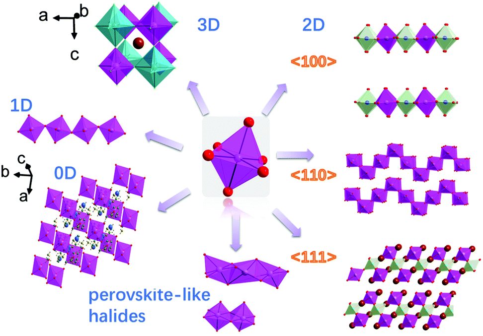 | ||
| Fig. 1 Standard-perovskites (3D), 2D perovskites with different types of layers (2D, 〈100〉, 〈110〉, 〈111〉), chains of octahedra in 1D perovskites, discrete octahedra separated by organic cations (0D) and perovskite-like halides with moieties of edge- and face-sharing octahedra. Aadapted with permission from ref. 37. Copyright (2018) American Chemical Society. Standard-perovskite structural characteristics. | ||
Space rules need to be followed: The typical perovskite structure is cubic with the space group Pm3m-Oh i.e., SrTiO3 and CsSnBr3.38 Take the perovskite-type oxides, ABO3 for example, where A is the larger cation and B is the smaller cation. In ABO3 structure, the B cation is 6-fold coordinated and the A cation is 12-fold coordinated with the oxygen atoms. The corner-sharing octahedra form the skeleton with the centre position occupied by the A cation.39 The crystal structure of the perovskite is very flexible, but certain rules must be met to ensure structural stability. The 3D-perovskites have the general formula ABX3. Goldschmidt's tolerance factor t and the octahedral factor (μ) have been used to screen and discover new halide perovskites,34 as the formulas shown below:
 | (1) |
 | (2) |
Electroneutrality: Another condition need to be fulfilled is electroneutrality, i.e. the sum of charges of cations should equal the total charge of oxygen anions. This can be obtained by appropriate charge distribution in the form of A1+B5+O3, A2+B4+O3 or A3+B3+O3. In addition the partial substitution of A and B ions by other cations is allowed. However, deficiencies at the A- or B-sites or of oxygen anions are frequent resulting in defective perovskites. WO3 is a representative of B6+O3 type peroskites with no A-site cations.40 The nonstoichiometry in perovskites has been widely discussed.39 Oxygen vacancies are more common than those of cations, e.g., Ca2Fe2O5 and La2Ni2O5. Ca2Fe2O5 can be considered as an anion-deficient perovskite with one-sixth of the oxygen ion sites being vacant.
Standard perovskite with single-type B-site cations: In the 3D perovskite structure, the octahedra are connected via corner-sharing to form a 3D network. The chemical formula corresponding to the octahedral unit is MX3, such as in SrTiO3, CsPbBr3 and MAPbX3 (X = Cl, Br, I)9,41 According to the tolerance factor, for halide perovskites, the A-site cation is limited to Cs, MA or HC(NH2)2+ (FA) filling the voids of the BX6 (X = Cl, Br, I) octahedral network. The B site is normally occupied by a divalent cation, such as Sn2+, Pb2+, Ge2+, Sr2+, Ca2+, Mg2+, Cu2+ or Ni2+.
Double perovskites: Double perovskites have the formula A2B′B′′O6 or A2B′B′′X6 (X = Cl, Br, I), where the primes indicate different ions in different oxidation states. Since the B cations generally determine the properties of perovskites, the different kinds of B′ and B′′ ions show a variety of properties. It was reported that the distortion of the double perovskite Sr2LnRuO6 from the cubic symmetry is mainly due to the tilting of the octahedra rather than the distortion of the octahedra.42 For halide perovskites, one valence Na+, Ag+, Cu+ or Au+ cation can take part in mixed occupancy with some trivalent cations, such as Sb3+, Bi3+ or In3+, to form double perovskites A2BB′X6.43–45 For more information, one can refer to the review published by Hoefler et al., in which the possible choices for B-sites are discussed in detail.46
2.1. Low-D perovskite structural characteristics
Recently, low-D halide perovskites with ordered vacancies or large separating organic cations have been developed to enhance the stability and/or for a reduced toxicity of the most promising 3D lead-containing halides (e.g. MAPbX3, FAPbX3), which showed a high conversion efficiency in solar cells. Low-D perovskites consist of sliced layers, corner-sharing chains, or clusters of the ABX3 structure.47 The low-D structure is less constrained by the tolerance factor than the 3D structure.Such a corrugated layer with ordered vacancies can also be found in organic–inorganic hybrid perovskites (OIHPs). (H2AEQT)M2/3I4 (M = Bi3+, Sb3+) possesses a 〈100〉-oriented single-layered structure, where the high-valent metal halide inorganic sheet is stabilized by vacancy formations at the metal sites. The inorganic sheet can be written as (M3+)2/3V1/3X4 (X = Cl, Br, I), where V represents a vacancy. Given a suitable organic cation layer, this may be further extended to include other higher priced metals. For tetravalent metals (e.g. Sn4+, Te4+, Hf4+), the inorganic anion layer can be represented as (M4+)1/2V1/2X42−, and for pentavalent metals (e.g. Nb5+, Ta5+, Mo5+) as (M5+)2/5V3/5X42− and (Mn+)2/nV(n−2)/nX42− for larger n. However, the vacancy concentration of the perovskite structure may become too high to make the structure stable.
Based on the A2B′B′′X6 (X = Cl, Br, I) double perovskite, a B-site cation can be replaced by a vacancy to produce an A2□BX6 perovskite. In order to maintain the charge neutrality of the structure, B must be a tetravalent cation. Because the two adjacent octahedra are not connected to each other A2BX6 forms 0D structures. A2BX6 containing Sn4+, Te4+, Pt4+ and Pd4+ cations have been reported, e.g. Cs2SnI6, Cs2TeI6,50 Cs2PdBr6![[thin space (1/6-em)]](https://www.rsc.org/images/entities/char_2009.gif) 51 and A2Pt□I6 (A = NH4+; MA+; FA+; and C(NH2)3+).52 Further, to broaden this family, the range of tetravalent cations can also be extended to Mn4+, Zr4+, Cr4+ and Ti4+, or a combination of these cations.
51 and A2Pt□I6 (A = NH4+; MA+; FA+; and C(NH2)3+).52 Further, to broaden this family, the range of tetravalent cations can also be extended to Mn4+, Zr4+, Cr4+ and Ti4+, or a combination of these cations.
Early in 1978, Arend et al.55 reported the synthesis, solubility and crystal growth of layered-structure halide perovskites with unbranched organic chains, such as (CnH2n+1NH3)2MX4 and NH3(CH2)mNH3MX4 with M = Cd, Cu, Fe, Mn or Pd, X = Br or Cl, n = 1, 2,…, 18, and m = 2, 3,…, 8. In 1985, Day reported layered perovskite halide salts (RNH3)2MX4 (R = organic group; M = Cr, Mn, Cd; X = Cl, Br).54 The ammonium groups hydrogen bond to the inorganic sheet by halogens, and the organic tails extend into the space between the layers, holding the structure together via van der Waals interactions. The organic–inorganic perovskite family has yielded a remarkable degree of structural versatility.56,57
According to the connection of the octahedral layers, the 2D perovskites can be divided into three structural types: (1) the 〈100〉-oriented perovskite; (2) the 〈110〉-oriented perovskite; (3) the 〈111〉-oriented perovskite (Fig. 1).12 Here, (1) and (2) have the general formula A′2An−1BnX3n+1 or A′An−1BnX3n+1 (A′ = 1+ or 2+; A = 1+ cation; B = Pb2+, Sn2+, Ge2+, Cu2+, Cd2+, etc.; X = Cl−, Br−, and I−), and (3) has the general formula A′n+1BnX3n+3 (n ≥ 1, where B valence is +3, or a mixed valence averaging +3, e.g. Cu2+ and Sb3+).58 According to a survey of the Cambridge Structural Database, the majority of 2D perovskites possess <100>-oriented layers, with the total number being approximately 250, and there are only a few reports on <110>-oriented structure.12,59–64
In <100>-oriented perovskites, the thickness of the inorganic layer (corresponding to an n value of A′2An−1BnX3n+1) can be controlled by adjusting the ratio between the spacer cations and the smaller cation, with the n value varying from 0 to ∞.65,66 Similarly, thicker layered 2D perovskites with both <110>- and <111>-oriented inorganic sheets can be obtained (Fig. 2a). We can regard the 3D perovskites as the extreme case of this 2D structure with n = ∞, and 2D perovskites as the case with n = 1.53,65,67,68 For <110>-oriented perovskites, depending on where the ripple occurs in the corrugated layer, the structures can be defined as 2 × 2, 3 × 3, 4 × 4, “n × n”, where n represents the number of octahedra making up half of the roof (Fig. 2b).63
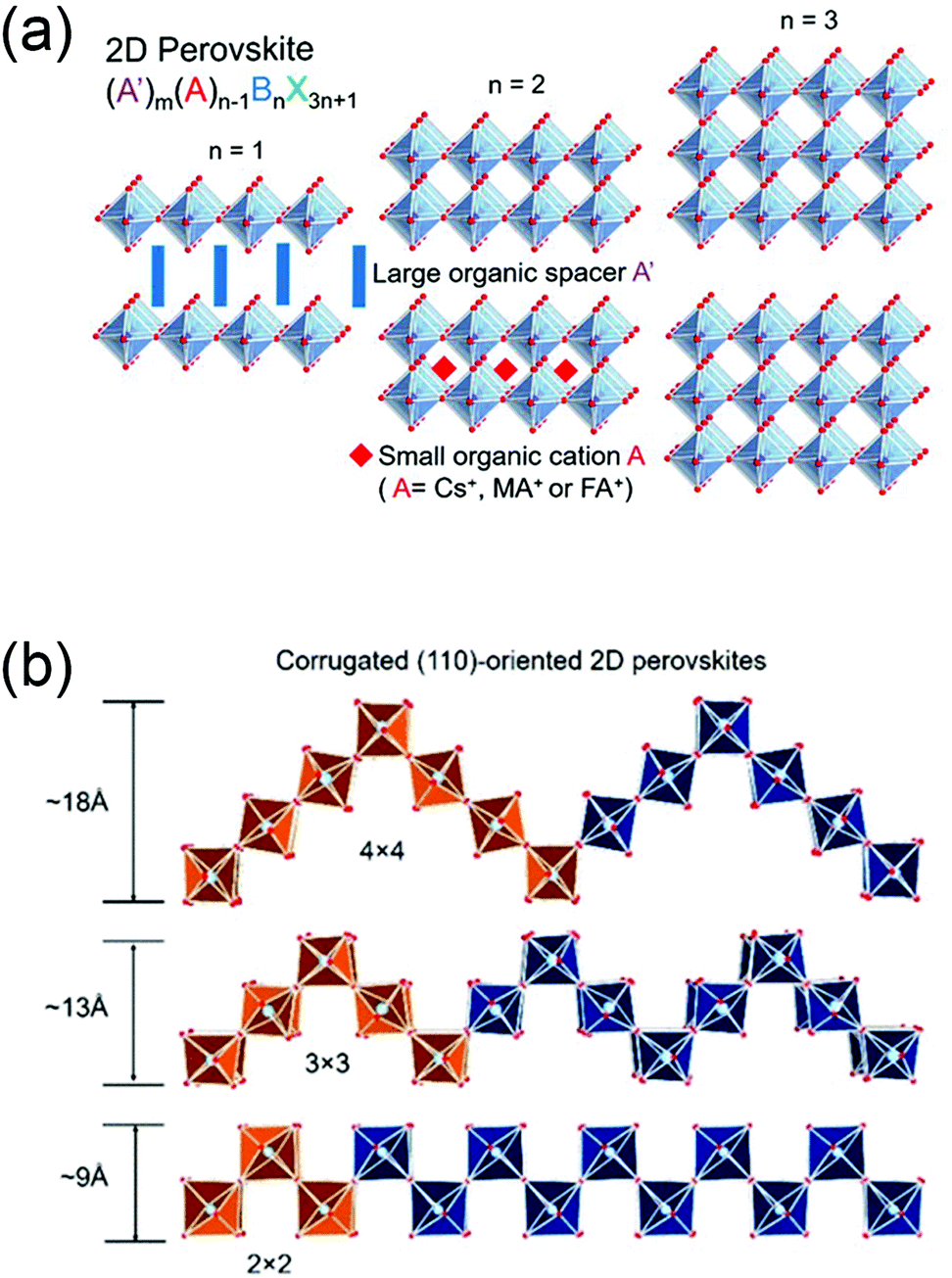 | ||
| Fig. 2 (a) The evolution from 2D perovskites to 3D perovskites, with the organic moieties omitted. Reprinted with permission from ref. 58. Copyright (2019) American Chemical Society; (b) corrugated (110)-oriented 2D perovskites with different members of half of the roof octhedra n. Reprinted with permission from ref. 63. Copyright (2017) American Chemical Society. | ||
1D and 0D perovskites. In the 1D perovskite structure, large organic cations separate the infinite chains formed by corner-sharing octahedra, with the unit chemical formula of MX5. The 0D perovskite structure preserves MX6 as the unit chemical formula, for which the isolated octahedra are non-interacting and are separated from each other by organic moieties. The 0D OIHP-forming B-site metals include Ti4+, Hf4+, Zr4+, Pd4+, Pb2+, Sn4+, Te4+, Sb3+, Mn4+, In3+, Bi3+ and Cr4+ or a combination of these cations.36,69
2.2. Structural characteristics of perovskite-like halides
Perovskite-like halides contain, but are not limited to, octehadra connected by edge-sharing or face-sharing octahedra forming different dimensional structures. This type of structure is weakly associated with perovskites, with the only common feature being that they contain six coordinated metal cations. Therefore, the structure only needs to satisfy the octahedral factor μ. In this review, we discuss the structure and PL properties of this type of perovskite for two main reasons: (1) many compounds with such structures and high PLQY have been reported recently, (2) so far, octahedral connection ways cannot be designed or predicted, and this type of structure occasionally appears when trying to synthesize low-D perovskites.2.3. Morphology and materials
Luminescent perovskite materials have a variety of morphologies. Zhu et al. systematically synthesized MAPbX3 (X = I, Br) NCs into dots, rods, plates and sheets by using different solvents and capping ligands.70 Morphology evolution is often related to the change in luminescent performance. The luminescence degradation of perovskite NCs mainly originate from the large CsPbBr3 crystals under illumination.71 Excitonic emission has only been observed in MAPbI3 single crystals, but not in MAPbI3 thin films72 The further application of lead halide perovskite materials is hindered by lead toxicity. Different non-lead perovskite NCs can be synthesized by replacing Pb2+ with other isoelectronic elements, such as Sn4+, Sb3+ and Bi3+.73,74 New synthesis methods have been developed besides the conventional solution-based colloidal process for perovskite NCs.75 Dirin et al. developed a method involving the infiltration of perovskite precursor solutions into the pores of mesoporous silica, followed by drying, leading to the template-assisted formation of perovskite NCs.76 Chen et al. reported the grinding synthesis of the whole family of MAPbX3, FAPbX3, and CsPbX3 (X = Cl, Br, I and their mixtures) perovskite NCs, which could be operated at room temperature and in the open atmosphere.773. Electronic structure and luminescence in perovskites
The luminescent properties of materials are dependent on their electronic structures; while the electronic structure is determined by the crystal structure and chemical composition. To obtain a full understanding of the luminescence in perovskites, it is necessary to study the electronic structure in perovskite materials. The band structure of a perovskite is closely related to its composition. In organic–inorganic hybrid perovskites, the inorganic layer dominates the luminescent properties. Compared with cation A, the octahedra [BX6] play a more crucial role in the formation of the perovskite electronic structure. For example, in MAPbI3, the conduction band minimum is mainly affected by the p-orbital electrons of the Pb atom, while the valence band top is mainly composed of the Pb s orbital and the I p orbital. The cation A can only adjust the band structure by changing the bending and stretching between Pb and the halogen atom in the [PbX6] octahedra.78,79 For example, the electronic structures between MAPbX3 (X = I, Br) and CsPbX3 are the same. The band gap of the hybrid organic–inorganic compounds CH3NH3SnI3 and NH2CHNH2SnI3 is very close to that of a hypothetical CsSnI3 cubic perovskite with the same cell size.80The luminescence in perovskites originates from the radiative processes, including band-to-band transition, electron–hole recombination and the transitions between emissive sub-band levels. Discussion on the core–valence luminescence in some scintillators, which involves the recombination of a core hole and a valence electron, is not included in this paper.81 Although some mechanisms have been established in a number of well-developed theories, further studies on the luminescent mechanism are continuing to contribute new insights. For example, there exists a debate about the relative ordering of dark and bright sublevels in halide perovskites. Becker et al. showed that a highly emissive triplet state is the lowest excitonic level in caesium lead halide perovskites (CsPbX3, with X = Cl, Br or I).82 On the contrary, Tamarat et al. proved that the dark singlet exciton state is located several meV below the bright triplet in formamidinium lead bromide (FAPbBr3) perovskite NCs.83 In Table 1, various luminescent properties are provided, including the mechanism (from impurities or excitons) and emission peak wavelengths.
| Material name | Luminescence mechanism* | Emission maximum (nm) | Ref. | Material name | Luminescence mechanism* | Emission maximum (nm) | Ref. |
|---|---|---|---|---|---|---|---|
| *: The letter “I” stands for impurity luminescence and “E” for excitonic luminescence. **: The luminescence in LaInO3 comes from In3+ as impurities.84 †: Cerium ion present in Sr2CeO4 is tetra-valent with no radiative emission. The luminescence originates from the host.98 | |||||||
| LaInO3:Bi3+ | I | 420 | 84 | Ba2CaTeO6:U6+ | I | 500 | 85 |
| CaZrO3:Bi3+ | I | 390 | 86 | KMgF3:Cu+ | I | 415 | 87 |
| LaAlO3:Bi3+ | I | 375 | 84 | NaMgF3:Cu+ | I | 375 | 87 |
| CaZrO3:Pb2+ | I | 365 | 88 | LiBaF3:Cu+ | I | 465 | 87 |
| LaInO3 | I** | 515 | 84 | (C10H21NH3)2PbI4 | E | 516 | 56 |
| NaMgF3:Eu2+ | I | 365 | 89 | YAlO3:Ce3+ | I | 370 | 90 |
| KMgF3:Eu2+ | I | 363 | 89 | LuAlO3:Ce3+ | I | 365 | 91 |
| RbMgF3:Eu2+ | I | 360 | 89 | BaTiO3 | E | 485 | 92 |
| CsMgF3:Eu2+ | I | 360 | 89 | (MeNH3)SnI3 | E | 761 | 93 |
| KCaF3:Eu2+ | I | 485, 520 | 89 | (MeNH3)(C10H21NH3)2Sn2I7 | E | 733 | 93 |
| RbCaF3:Eu2+ | I | 475 | 89 | (C10H21NH3)2SnI4 | E | 603 | 93 |
| CsCaF3:Eu2+ | I | 510 | 89 | (MeNH3)SnBr3 | E | 576 | 93 |
| RbSrF3:Eu2+ | I | 424 | 89 | (MeNH3)(C10H21NH3)2Sn2Br7 | E | 517 | 93 |
| CsSrF3:Eu2+ | I | 426 | 89 | (MeNH3)PbCl3 | E | 408 | 93 |
| Ba5Ta4O15 | E | 455 | 94 | (C10H21NH3)2PbCl4 | E | 336 | 93 |
| Ba5Nb4O15 | E | 575 | 94 | (C6H5C2H4NH3)2PbI4 | E | 520 | 95 |
| KTaO3 | E | 490 | 96 | (C6H9C2H4NH3)2PbI4 | E | 510 | 97 |
| LiTaO3 | E | 340 | 96 | Sr2CeO4 | E† | 485 | 98 |
| NaTaO3 | E | 440 | 96 | (C6H5C2H4NH3)2PbBr4 | E | 406 | 99 |
| KLaNb2O7 | E | 590 | 100 | (C6H5C2H4NH3)2PbI4 | E | 520 | 99 |
| K2La2Ti3O10 | E | 475 | 101 | (C4H9NH3)2SnI4 | E | 616 | 99 |
| Gd2MgTiO6:Mn4+ | I | 681 | 102 | KMgF3:Ce3+ | I | 350 | 103 |
| BaLaLiWO6:U6+ | I | 538 | 104 | LiBaF3:Ce3+ | I | 325 | 103 |
| Ba2SrWO6:U6+ | I | 512 | 104 | CsPbCl3 | I | 418 | 105 |
| Sr2MgWO6:U6+ | I | 504 | 104 | (C4H9NH3)2PbBr4 | I | 412 | 106 |
| (C4H9NH3)2EuI4 | I | 460 | 107 | SrSnO3 | E | 425 | 108 |
| Ba2MgWO6:U6+ | I | 510 | 85 | Ba2CaTeO6:U6+ | I | 500 | 85 |
3.1. Band gap and affecting factors
The electronic structure plays a vital role in the luminescent properties of perovskites. The forbidden band-gap energy is influenced by both the crystal structures and chemical components. The effect of dimensionality will also be discussed.Crystal structure factor. For the perovskite structure, the octahedral tilting distortion is the main factor.109 In the alkaline-earth stannate perovskites (BaSnO3, SrSnO3 and CaSnO3), the conduction bandwidth decreases strongly in response to the octahedral tilting distortion, triggered by the decreasing size of the alkaline-earth cation. This in turn leads to a corresponding increase in the band gap from 3.1 eV in BaSnO3 to 4.4 eV in CaSnO3.110 The band gap of CdSnO3 is relatively small (3.0 eV) considering the large octahedral tilting distortion. The anomaly stems from the mixing between the empty Cd 5s orbitals and the antibonding Sn 5s–O 2p states, which leads to a widening of the conduction band and a corresponding decrease in the band gap. For pyrochlores (Re2Sn2O7, Re = Y, La, Lu), the Sn–O–Sn bonds are highly distorted from the linear geometry in pyrochlore, leading to a relatively narrow conduction band and a wide band gap. In Cd2Sb2O7 and defect pyrochlore oxides Ag2Sb2O6, the Cd2+ and Ag+ ions exhibit a strong inductive effect, which widens the conduction band and lowers the band gap significantly, very similar to the effect observed in the perovskite form of CdSnO3.110
Composition factor. Although the variation in chemical composition also induces a change in the crystal structure, the contribution from the chemical component could be prominent in crystal structures with great similarity. The band gaps of AgTaO3 and AgNbO3 are 3.4 and 2.8 eV, respectively, being 0.6 eV smaller than the band gaps of NaTaO3 (4.0 eV) and NaNbO3, although the crystal structures of AgMO3 are similar to those of NaMO3.111 Using the plane-wave-based density functional method, it was found that a hybrid orbital of Ag 4d and O 2p forms a valence band at a more negative level than O 2p orbitals, resulting in a decrease in the band gap. A full band gap range of 1.6–2.3 eV could be modulated through MAPbI3−xBrx perovskite films.15 With the change of the mixed-halide, the full-spectrum luminescence (410–700 nm) of CsPbX3 can be realized.112 Transition metal oxide perovskites usually possess large energy gaps (>3 eV) due to the large energy differences between the transition metal d-orbital conduction band and the O 2p orbital valence band. By replacing O with S or Se in transition metal chalcogenide perovskites, the valence band composed of mainly chalcogen (S, Se) 3p or 4p orbitals could be shifted higher and the band gaps could be decreased to the visible-IR range.113
Dimensionality factor. The effects of dimensionality on the band gap could be analyzed from the viewpoint of the inductive effect and charge transfer process. Mitzi et al. found that in the layered compound (C4H9NH3)2EuI4, the luminescence peak occurs at 460 nm, while for the 3D system, CsEuI3, the emission peaks at 449 nm.107 In this case, the 3D crystal structure widens the band and subsequently narrows the band gap. In other words, breaking the corner-sharing octahedra network increases the band gap. Similarly, the band gaps of Sr2SnO4, Sr3Sn2O7 and SrSnO3 decrease as 4.43 (280 nm), 4.13 (300 nm) and 3.88 eV (320 nm), respectively.114 The optical band gaps of A(La0.98Bi0.02)Ta2O7 (A = Rb, K, and Na) phosphors were measured by their diffuse reflection spectra and estimated to be about 4.10, 3.94 and 3.96 eV, because the 2D perovskite layers are less separated in the sequence Rb, K, Na.115 In the 3D perovskite crystal structure with interconnecting octahedra, the band gap could be widened by smaller A cations with larger electronegativity. The band gap of (Ba1−xSrx)2YSbO6:0.005Mn4+ changes from 4.50 to 4.72 eV as the Sr2+ content increases from x = 0 to 1.0.116 Through the compositional modulation with increasing Rb, the band gap and emission spectra of RbxCs1−xPbBr3 are readily tunable over the visible spectral range from 532 to 474 nm.117 The dispersive band edges of CsPbBr3 do not support self-trapped carriers, which agrees with reports of a weak exciton binding energy and high photocurrent. The larger gap 0D material Cs4PbBr6, however, has revealed polaronic and excitonic features.118
The low-Dl structure results in a dielectrically restricted exciton binding energy increase due to the difference in dielectric constant between organic ions and [BX6] octahedra. Therefore, when gradually increasing the n value, the dimension of the 2D perovskite increases, and the well width of the quantum well increases correspondingly, resulting in weaker exciton binding energy, a reduced band gap and a red-shift of the emission peak. As direct band gap semiconductors, OIHPs have inherent advantages in terms of their conductive and luminous properties, and their band gaps can also be tuned by regulating the inorganic element components.119,120 Quantum wells are very good fluorescent materials, and their photoluminescence can be rooted to various emission mechanisms, including strongly correlated electron–hole pairs, which are known as free excitons (Fes), permanent lattice defects, transient light-induced defects, like self-trapped excitons (STE), and coordination of the inorganic layer and molecular chromophores.
To obtain a full understanding of the luminescence in perovskites, it is necessary to study the electronic structure in perovskite materials. In OIHPs, the inorganic layer dominates the luminescent properties. For example, the electronic structures between MAPbX3 (X = I, Br) and CsPbX3 are the same. Moreover, the material dimensionality also has an effect. Tuning the average crystallite dimension in methylammonium lead trihalide perovskite thin film from tens of nanometres to a few micrometres reveals that larger crystallites present a smaller band gap and longer lifetime.121
Other factors. The band gaps are also related to the temperature and synthesis conditions. For example, the band gaps of MAPbI3, MAPbBr3 and FAPbBr3 exhibit an unusual blue-shift when raising the temperature from 15 to 300 K, caused by the stabilization of the valence band maximum.122 The band gap of Cs2AgSbCl6 could be tuned by adding different volumes of HCl during synthesis.123
3.2. Understanding the electronic structure from the viewpoint of charge transfer and the inductive effect
Charge transfer in OIHPs has been addressed as the resonant interaction between Wannier excitons in inorganic materials and Frenkel excitons in adjacent organic layers.124,125 However, in this paper, charge transfer is mainly focused on the inorganic part, which is commonly regarded as involving a transfer of charge from a ligand anion (oxygen or halide) towards the central metal cation (Ti4+, Pb2+) in the octahedral coordination. In reality, no electron is transferred in the transition, but a considerable reorganization of the charge density distribution around the metal is expected. This reorganization is accompanied by an expansion of the metal–ligand bonds in the excited state, which gives rise to the observation of a large Stokes shift and broad bands.The absorption edge in perovskites consisting of a highly charged cation with a noble gas configuration and oxygen ions is usually caused by charge-transfer transition. As can be seen in Fig. 3, an electron from the highest filled molecular orbital localized on the oxygen ions is transferred to the lowest empty molecular orbital localized on the highly charged ion, which is mainly 5d(t2g) for the tungsten ion. Blasse and Corsmit found from the reflection spectra of A2BWO6 compounds that the absorption edge is mainly dependent on the A element and weakly influenced by the B element.126
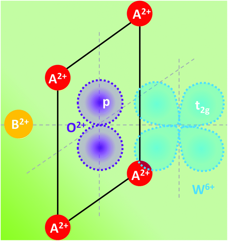 | ||
| Fig. 3 Local anion coordination and schematic shape of the molecular orbitals involved in the charge-transfer transition in the perovskite A2BWO6. Redrawn from ref. 108, Copyright (1973), with permission from Elsevier. | ||
With the increase in the ionic radius of A or B, the absorption edge is continuously shifted to longer wavelength. To elucidate the charge-transfer mechanism, the local coordination and the relevant orbitals are redrawn. The absorption corresponds to an electronic transition from the occupied oxygen 2p orbitals to the empty tungsten t2g orbitals. Since the spectral position of the charge-transfer band depends on the charge and on the radius of the coordinated cations, it is reasonable that the oxygen valence electron feels a weaker field as the A or B ion increases in ionic radius, and therefore less energy is needed to initiate the electron transfer to the highly charged tungsten ion. Consequently, the charge transfer is more sensitive to the four coordinated A ions than the only one coordinated B ion, even though the B ion is located closer to the tungstate group than the A ion.
In this sense, some of the key factors in luminescent perovskites could be understood from the viewpoint of charge transfer and the inductive effect. Exciting one electron from the valence band maximum to the conduction band minimum across the band gap energy could be imagined as a charger transfer from the atomic orbital constituting the valence band to that constituting the conduction band. Meanwhile, since the electron–hole pair of an exciton is created by photon absorption, the process could also be regarded as the charge transfer of one electron from the full valence band to the empty conduction band, with one hole left in the valence band. As a result, the charge-transfer energy could be analyzed by considering the inductive effect.127 Take an ABO3-type perovskite material for example. With a smaller electronegativity of A (larger ionic radius with the same valence state), the electron in ligand O is less attracted by A, and the central B takes less energy to transfer an electron charge from the ligand O. On the other hand, the lower electronegativity of the ligand also favours the charge-transfer process. In CsPbX3 (X = Cl, Br, I), the excitonic luminescence spectra could be obtained from blue to red as the ligand changes from Cl to I, with decreasing electronegativity. The tuning the light emission wavelength of 2D CsPbBrxCl3−x perovskite films from green (504 nm) to blue (470 nm) could be realized through compositional engineering via increasing the content of chloride.128
3.3. Interband/exciton luminescence
In semiconductors and insulators, optical transitions across the fundamental band gap excite an electron towards conduction, with a hole created in the valence band. Annihilation of an electron–hole pair leads to interband luminescence, which is also known as radiative electron–hole recombination. However, the band gap energy is usually difficult to determine due to the presence of an exciton. Dorenbos proposed that the band gap energy could be estimated by 1.08 × Eex, where Eex is the energy needed to produce an exciton, and the factor of 1.08 means the electron–hole binding energy of the exciton.129 So the defined mobility band edge energy is much larger (≈15%) than the fundamental optical absorption band edge energy.Interband luminescence. The excitonic level is located quite close to the conduction band, such that it is difficult to distinguish interband luminescence from exciton luminescence in some materials. The pronounced conductivity dependence of the emission intensity in SrTiO3 suggests a direct recombination of the conduction electrons and the oxygen 2p valence band holes.130,131 Jellicoe et al. observed two luminescent decay channels in CsSnX3 (X = Cl, Br, I), which were assigned to a fast band-to-band emission and a slow radiative recombination at shallow intrinsic defect sites.73
Generally, there exist two types of excitons, Frenkel and Wannier excitons. An exciton can be understood as a single excited electron taken out of a band full of electrons according to band theory, which provides a basic description of the electronic states. Band theory claims that all states in the full valence bands correspond to the ground state of the crystal, and in the meantime, all the states in the conduction bands are empty. A hole–electron pair is created in the process of exciting an electron from the valence to the conduction band across the forbidden gap under light absorption. The Coulomb attraction between the electron–hole pair lowers the formation energy of the hydrogen-like state compared to that given by band theory. By solving the Schröndinger equation for a hypothetical 2D hydrogen atom, Shinada and Sugano found that a small peak may appear just above the absorption edge because of the Coulomb interaction between an excited electron and a hole.132 The exciton may be described by the effective-mass approximation when the interaction is weak in a medium with a high dielectric constant.133 Frenkel introduced the concept of an exciton as “excitation quanta”.134 That is, an excitation wave formed by exciting individual atoms to higher atomic states can be associated with an “excitation quantum” similar to a light quantum. Under interatomic interactions, the motion of this excitation quantum represents the motion of the excitation travelling through the crystal. Its energy is related to the energy difference between the excited and the normal state. In Frenkel's description, in the case of a strong Coulomb interaction, the hole–electron pairs are confined to a single atom, but the excitation state could be cruising from atom to atom.
Wannier found that in the states located near the bottom of the excited Bloch band, the electron cannot escape its hole completely, and no photocurrent can be observed.135 Discrete states are included in the lower part, in which the widely spaced lowest states correspond to the excitation of an electron within its cell or to some direct neighbour. The discrete energy spectrum is obtained for bounded excitons. This individual character disappears at the higher states with narrower spacing, in which the electron moves in the Coulomb field of its hole. Furthermore, the continuous Bloch band follows with the electron and hole moving independently, and a current may be observed. Therefore for unbounded excitons, a continuous energy spectrum could be obtained. The free-exciton emission is usually caused by band-gap excitation and has a narrow-band feature.
Exciton luminescence. The luminescence of inorganic–organic hybrid perovskites based on metal halide sheets and optically inert organic cations arises from the exciton states associated with the band gap of the metal halide framework. For example, in the multilayer perovskites (C4H9NH3)2(CH3NH3)n−1(Ge,Sn,Pb)nI3n+1, intense room-temperature photoluminescence has been observed with wavelengths ranging from the ultraviolet through the red spectral region in the germanium(II)-, tin(II)- and lead(II)-based systems.107 The luminescence originates from the radiative decay of the FEs associated with the 2D inorganic layers in the structure. It should be noted that the luminescence properties of the organic–inorganic hybrid compounds may be governed by the excitonic properties of the inorganic layer.136 The emission wavelength is tunable through the choice of metal atom, halogen or the thickness of the perovskite sheets. It should be noted that in the purely inorganic PbI2, the room-temperature exciton luminescence is quenched because of the small exciton binding energy (approximately 30 meV). Small exciton binding energies of 32 and 41 meV have also been observed for (CH3NH3)PbI3 and MAPbCl3, respectively, which have 3D perovskite structures.137,138 On the contrary, the exciton binding energies in lead(II)-based organic–inorganic perovskites approximate 200–400 meV, leading to strong room-temperature excitonic photoluminescence.107 The increase in binding energy is caused by both the quantum confinement effect (two dimensionality of the structure) and the smaller dielectric constant of the interleaving organic layers sandwiching the metal halide sheets, which enhances the electron–hole Coulomb interaction. For example, in the layer-type perovskite structure of (C10H21NH3)2PbI4, the PbI4 layers are sandwiched by alkylammonium chains as barrier layers. The perovskite has a large excitonic binding energy of 370 meV, originating both from the 2D characteristic and the small dielectric constant of the barrier layer, with the latter one achieving a much stronger Coulomb interaction between an electron and a hole.139
Besides, the excitonic emission wavelength is largely affected by the dimensionality or thickness of the inorganic layer, which could also be explained by the quantum confinement. Generally, quantum confinement leads to a spectral blue-shift towards high energy.140 In (C10H21NH3)2(CH3NH3)n−1PbnI3n+1, as the thickness (n) of the perovskite sheets increases from n = 1 to the 3D n = ∞ compound (i.e. MAPbI3), the luminescence shows a substantial peak shift towards longer wavelength from 524 nm to 753 nm.107 This phenomenon in the luminescence spectrum can be understood by a band gap reduction with the increasing perovskite sheet thickness, because the bands are more easily formed as the dimensionality increases. Tabuchi et al. modulated the inorganic layer thickness in the layered perovskites compounds (CnH2n+1NH3)2(CH3NH3)m−1PbmBr3m+1 by changing the ratio of the two amines (CnH2n+1NH3/CH3NH3).141 The strong, clear excitonic absorption peak of the layered perovskite films measured at room temperature was caused by the large exciton binding energy. With increasing the number of inorganic layers from 1 to 3, a red-shift of the excitonic absorption was observed because of the decrease in transfer energy among the inorganic network.
A smaller dielectric constant has the ability to reduce the dielectric screening of the Coulomb interaction between electrons and holes. Compared to MAPbI3, MABrI3 has a lower dielectric constant because of the larger band gap energy.142 This results in a smaller Bohr radius and larger binding energies of the excitons in MAPbBr3. Meanwhile, the smaller extent of the exciton wave function is reflected by a larger oscillator strength.
White-light (WL) emission could be obtained in thin films of (C6H11NH3)2PbBr4 resulting from the broad-band, strongly Stokes shifted STE emission.156 Hu et al. showed that the broad-band Stokes shifted emission in the 2D hybrid perovskite (N-MEDA)[PbBr4] (N-MEDA = N1-methylethane-1,2-diammonium) originated from a photogenerated energy distribution of STE states. Almost no potential barrier exists for the transition from FE to STE due to strong electron–phonon coupling, enabling ultrafast formation of the STE states on a femtosecond timescale.157 Cortecchia et al. conducted a combined, systematic spectroscopic and computational study of the WL emission properties of the layered organic–inorganic perovskites (EDBE)PbCl4 and (EDBE)PbBr4. Due to strong Coulomb interactions, the formation of Pb3+ and X− (where X = Cl or Br) species were confined within the inorganic perovskite framework, forming self-trapped polaron–excitons.158 0D perovskites structurally impose carrier localization and result in the formation of localized Frenkel excitons. In 0D perovskite-derived Cs4SnBr6, the substitution of Cs+ by Rb+ or K+ results in a blue-shift of the emission. For 25% substitution, Rb+ and K+ shift the PL peak from 540 nm to 519 and 500 nm, respectively.69 This phenomeon could also be understood from the viewpoint of the inductive effect, which states that cations occupying an A site with a smaller electronegativity are in favour of STE. However, semiconductors generally suffer from severe luminescence quenching due to an insufficient confinement of excitons (bound electron–hole pairs). Sn-Triggered extrinsic self-trapping of excitons in the bulk 2D perovskite crystal PEA2PbI4 (PEA = phenylethylammonium) has the ability to improve the luminescence, as reported by Yu et al.159 However, STE never occurs in the pure state without Sn. The isoelectronic Sn dopants initiate the localization of excitons by inducing a large lattice deformation around the impurities for STE accomodation. The STE luminescence in Sn-doped perovskites generates a broad-band red to near-infrared (NIR) emission at room temperature.
Perovskite-like niobates and tantalates, such as KNbO3, KTaO3, Sr2Nb2O7 and Sr2Ta2O7, have corner-sharing NbO6 or TaO6 octahedra. They show non-efficient luminescence, which is fully quenched at room temperature. Blasse and Brixner argued that the luminescence originates from self-trapped exciton recombination on NbO6 or TaO6 octahedra, because corner-sharing octahedra are favourable for energy-band formation, i.e. electronic delocalization.160 From the viewpoint of the crystal structure, it is the angles of the M–O–M bonds that are important for delocalization.13 Similar results were also observed in niobates MNbO3 (M = Li, Na, K),161 tantalates MTaO3 (M = Li, Na, K)96 and perovskite-derived Ba5Ta4O15 and Ba5Nb4O15.94 For lanthanide metal ions-doped K2La2Ti3O10, the impurity luminescence could be observed by the host excitation. The energy transfer from the host to the rare-earth ions included both resonant energy transfer and a hole trapping mechanism. Moreover, the persistent luminescence and thermoluminescence observed in Tb3+- and Pr3+-doped K2La2Ti3O10 indicated a hole trapping process accompanying the valency change of the Tb and Pr ions.101
3.4. Luminescence from defects and impurities
Usually defects and impurities are detrimiental to luminescence as they can act as quenching centres. However, they could serve as luminescent centres by providing sub-band-gap states in the forbidden gap and induce radiative transitions from those levels.Bode and van Oosterhout noticed the defect luminescence in the ordered perovskite A2BWO6(Ba2MgWO6, Ba2CaWO6), which showed two different emission bands.165 Macke ascribed the two emission bands in the ordered perovskite La2MgSn1−xTixO6 to a regular titanate centre and a defect centre.166 Energy transfer from the regular to the defect centre was also observed. By comparing the luminescent properties between the undiluted titanate and the titanate with tin, it was found that in La2MgTiO6 defect luminescence dominated. Kobayashi et al. reported to defect luminescence in CsPbCl3. They observed two emission peaks, with a fast narrow band at 415 nm close to the band gap and a slower broad one at 600 nm, which suggested a defect origin.167 An interesting NIR emission peak at 930 nm was observed for Fe doped in SrSnO3 by Muralidharan et al., originating from the defective states of oxygen vacancies.168
Chirvony et al. found the dual effects of traps in methylammonium lead bromide perovskite NCs. Although they found that a nonradiative deactivation of the charge carrier occurred at traps, the longer (up to microseconds) luminescent decay components revealed that the traps also acted as a carrier reservoir, resulting from the rapid reversible multiple trapping and detrapping of carriers. The dark states (traps) and bright excitonic states were in dynamic equilibrium, which resulted in long lifetime luminescence.169
Recently, Dorenbos systematically studied how the lanthanide ion levels change with the chemical composition and structure of inorganic compounds.129 On the basis of the charge-transfer model and the chemical shift, the host referred binding energy schemes (HRBE) and vacuum referred binding energy schemes (VRBE) can be constructed.
These two schemes are often called “Dorenbos diagrams”, and can well account for the optical properties, such as for lanthanide-doped LaAlO3 and Pr3+-doped (Ca,Ti)1−x[Na,Nb]xO3 perovskite compounds,171,172 as shown in Fig. 4(a) and (b).
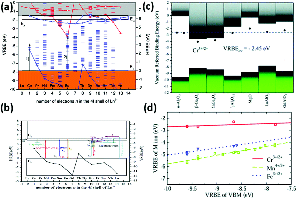 | ||
| Fig. 4 (a) VRBE scheme for LaAlO3. Arrow (1) indicates the energy of the CT-band maximum for Ce4+ and arrow (2) for Eu3+. (b) HRBE and VRBE schemes of Ln3+-doped (Ca1−xNax) [Ti1−xNbx] O3. The 4f ground states (Ln3+:4f) are labelled by the black inverted triangle and connected by solid curves. (E1: energy of the electron trap depth, E2: energy of O2–Ti4+/Nb5+ CT, E3: energy of IVCT, E4: electron transition energy from the top of the valence band to 3H4, E5: the band energy. (c) Stacked VRBE schemes for the acceptor levels of Mn4+/3+, Fe3+/2+ and Cr3+/2+ in different phosphors. The valence and conduction bands are represented by the bottom and top bars, respectively. The solid data point is the VRBE of those acceptor levels in a specific compound. Horizontal dashed line denotes the average VRBE for those acceptor levels. (d) VRBE of Cr3+/2+, Fe3+/2+ and Mn4+/3+ as a function of the VBM of different aluminates with octahedral sites. Panels adapted from: a, ref. 171, ©IOP Publishing. Reproduced with permission. All rights reserved; b, reprinted from ref. 172, Copyright (2017), with permission from Elsevier; c and d, reproduced from ref. 173 with permission from The Royal Society of Chemistry. | ||
Perovskite-type compounds can act as hosts to accommodate a large variety of impurities, including transition metal elements, lanthanide (rare-earth) elements, trivalent bismuth,84 divalent lead88 and hexavalent uranium.104 An extensive cation substitution is allowed in the high-symmetry perovskite or low-symmetry derived perovskite structures. Luminescence from impurities arises from a more local excitation and is therefore less sensitive to the overall dimensionality.
For example, the luminescent peak of CH3NH3EuI3 has approximately the same wavelength as that of CsEuI3. Consequently, the emission peaks for the Eu2+ family of 3D perovskites and the 2Dlayered system occur at very similar wavelengths.107 The luminescence could be induced by direct transition from the ground to excited state, and from energy-transfer and charge-transfer processes. The undoped LaInO3 gives a weak green luminescence resulting from In3+ acting as a luminescent centre via charge-transfer transition.84 Hair and Blasse found green emission with vibronic lines of the U6+ ion in the ordered perovskites Ba2MgWO6 and Ba2CaTeO6.85 They ascribed the excitation and emission bands to charge-transfer transitions. (C4H9NH3)2EuI4 was the first example of a layered organic–inorganic perovskite with a divalent rare-earth metal in the perovskite sheets.107 It produces intense blue photoluminescence at room temperature, with a peak wavelength of 460 nm, arising from a more localized excitation between the Eu2+ ground state, 4f7, and the 4f65d1 configurations other than the radiative decay of mobile Wannier excitons to produce luminescence. The transitions between the crystal-field levels of transition metal elements display a complex structure composed of zero phonon lines (ZPLs) and broad phonon sidebands caused by electron–phonon interactions.174 However, Rodriguez et al. argued that it is the vibronic sidebands related to phonons rather than the vibrational local modes of the localized centre that have the most affect.175 In the emission spectra of KMgF3:Mn2+ and KZnF3:Mn2+, sharp ZPLs were observed on the high energy side at 581 nm and 571 nm, respectively. A nephelauxetic effect results in the centroid shift of excited states for luminescence centres. By increasing the degree of covalency, a spectral shift towards long-wavelength is observed from CaZrO3:Bi3+ to LaInO3:Bi3+.84 The choice of compositional component has a large affect on perovskite luminescence. In ABF3:Eu2+ (A = Na, K, Rb, Cs; B = Mg, Ca, Sr), both 5d–4f wide-band emission and 4f–4f sharp-line emission co-exist when B = Mg, but only wide emission exists when B = Ca.89 The reason for this lies in the relative energy position of the lowest excited 4f and the lowest 5d levels, which is supposed to be determined by the crystal-field strength. The crystal field of Eu2+ sites is very weak in AMgF3, and consequently the lowest 5d level of Eu2+ is located at higher energy, which means 5d–4f band-emission occurs at short wavelengths. This is thus favourable for the occurrence of 4f–4f sharp-line emission.
Charge-transfer transitions have been widely observed in closed-shell transition metal-176,177 and trivalent lanthanides (Eu3+, Sm3+, Tm3+, Yb3+)-doped perovskites as the first absorption band, in contrast to Ce3+, Pr3+ and Tb3+, for which a 4f–5d transition acts as the first band.178,179 Generally the bandwidth of the charge-transfer band is twice as large as that of the f–d band.180 Meanwhile, lanthanide luminescence could be implemented by an energy transfer from the charge transfer band, such as the luminescence enhancement of Nd3+ or Ho3+ by combination with UO22+.181 The host absorption in the Eu3+-doped ionic conductor KGdTiO4 is mainly ascribed to the charge transition from the O-2p to Ti-3d states.182 In Yb3+ (4f13), the excited 4f state, 2F5/2, is located 10000 cm−1 above the ground state 2F7/2. Charge-transfer luminescence is widely reported because of the large energy difference between the charge transfer state and the highest excited 4f state.183 When Yb3+ is incorporated in a lattice at a larger cationic site, the relaxation in the excited charge-transfer state is larger and therefore the Stokes shift is larger.
The unusual luminescence in Sr2CeO4 originates from a ligand-to-metal Ce4+ charge transfer,98 not the isolated valence transitions, since the tetravalent state of cerium usually shows no luminescence. The excitation and emission spectra displayed broad maxima at 310 and 485 nm, respectively, and had a lifetime of 51 μs, which is uncharacteristically long compared to Ce3+ excited states.184 Danielson et al. confirmed by electron spin resonance and magnetic susceptibility that no significant amount of Ce3+ was present in the synthesized SrCeO4. The crystal structure here consisted of linear chains of edge-sharing CeO6 octahedra parallel to the c axis, and it was this low-D structure with terminal O ligands that was crucial to the observation of luminescence in Sr2CeO4. The O atoms in the equatorial plane were shared by two adjacent Ce4+ centres by edge sharing, with the two remaining terminal O atoms bonded to only one Ce4+. The highly ionized Ce4+ and the electron-rich O atom made it possible to facilitate the excited state based on O2− to Ce4+ ligand-to-metal charge transfer. On the contrary, in the 3D perovskite SrCeO3, for which a 3D network was formed by corner-sharing octahedra, no luminescence could be observed. It is possible that the low-D structure stabilized the exciton created by the charge-transfer process.
The 4d and 5 d electrons are less tightly bound to the core ion in comparison with the 3d electrons, and therefore charge-transfer transitions take place much easily. This transition is a parity-allowed electric dipole transition, and usually causes strong and broad bands.
Recently Qu and Dorenbos et al. conducted research to predict the location of the defect levels induced by 3d transition metal ions at octahedral sites of aluminate phosphors.173 Su et al. gave a brief overview of the crystal field calculations and DFT-based techniques to provide a complementary picture of the electronic structure and optical properties of transition metal- and lanthanide-doped materials, and showed that it is possible to locate the lowest state and all excited state energy levels of an impurity in the host band gap.186
3.5. Quantum dots and wells
With the decrease in material dimensionality or crystal structure dimensionality, the quantum confinement effect is enhanced, leading to quantum dot and well effects, particularly when at least one dimension is less than about 10a, where a is the Bohr radius of the exciton in the equivalent bulk material. Pronounced high-energy shifts have been observed as a consequence of the spatial confinement of the exciton motion in aggregates, with respect to the direct excitonic transition in the equivalent bulk material.:Pb ratio in the reactant and the reaction temperature.202 With the assistance of a fatty acid-capped precursor, He et al. managed to obtain a controlled morphology of CsPbBr3 NC nanowires to nanoplates, with the thickness varying from 5–7 monolayers.203
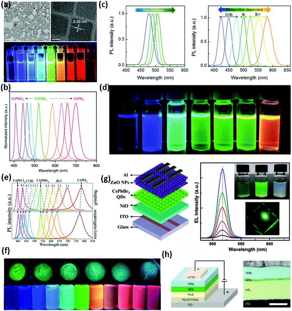 | ||
| Fig. 5 (a) Transmission electron microscopy (TEM) and high-resolution TEM images of CsPbX3 perovskite quantum dots. The scale bars represent 100 nm and 5 nm from left to right, respectively. (b) PL spectra (λ = 360 nm) of CsPbX3 perovskite quantum dots. (c) Size-dependent PL spectra of monodisperse perovskite CsPbBr3 quantum dots and composition-tunable PL spectra of perovskite CsPbX3 quantum dots by adding different halides. (d) The corresponding sample of perovskite CsPbX3 quantum dots. (e) PL spectra of FAPbX3 NCs prepared by a grinding method and supersaturated recrystallization route. (f) Corresponding luminescence photographs of FAPbX3 NCs under irradiation of a UV (365 nm) lamp. (g) Schematic illustration of solution-processed perovskite LEDs with a multilayered structure of Al/n-ZnO NPs/CsPbBr3 QDs/p-NiO/ITO. Coating solutions of C10H14NiO4 in acetonitrile, CsPbBr3 QDs in hexane and ZnO NPs in chlorobenzene. EL spectra measured at different voltages, together with a typical emission photograph of the LED with an active area of 2 × 2 mm2 (at 5.0 V). (h) Illustration of a multilayer perovskite QLED device. Left: The device structure. Right: Cross-sectional TEM image showing the multiple layers of the material with a distinct contrast. Panels adapted from: a and b, ref. 187; c,d and h, reprinted with permission from ref. 188. Copyright (2015) John Wiley & Sons, Inc.; e and f, reprinted with permission from ref. 77. Copyright (2019) American Chemical Society. g, reprinted with permission from ref. 189. Copyright (2018) American Chemical Society. | ||
The Cs4PbBr6 NCs have aroused debate over their luminescent property.204 They have a 0D crystal structure compared to the 3D structure of CsPbBr3. Their emission colour could also be tuned through the visible-light spectral region through halogen composition modulation. The narrow line-width luminescence originates from exciton recombination confined in the [PbBr6]4− octahedra, with a large exciton binding energy of 222 meV.205 Although both Cs4PbBr6 and CsPbBr3 produce remarkably intense green luminescence, a much longer lifetime is observed in Cs4PbBr6.206 Chen reported that the luminescence of CsPbBr3/Cs4PbBr6 composite originates from CsPbBr3 NCs.207 Lian also ascribed Cs4PbBr6 to be optically inactive in a CsPbBr3/Cs4PbBr6 composite.208 Riesen et al. concluded that the green emission from Cs4PbBr6 is due to nanocrystalline CsPbBr3 impurities, as assessed by undertaking cathodoluminescence imaging, which clearly showed the presence of small crystals, with emission peaking at 520 nm, embedded in/or between larger crystallites of Cs4PbBr6.209 Zou et al. changed the non-luminescent Cs4PbBr6 to blue-emitting NCs by incorporating Sn cations.210 On the other hand, some researchers think the photoluminescence in Cs4PbBr6 is independent of the presence of CsPbBr3 NCs.211 Zhang reported the tunable wavelength from 340 to 378 nm in the 0D perovskite Cs4PbX6.212 Adhikari confirmed the intrinsic luminescence nature of the Cs4PbBr6 crystals by varying the amount of the Cs-oleate precursor to convert CsPbBr3 with a strong blue emission (462 nm) to lead-depleted Cs4PbBr6 crystals with a green (529 nm) emission.213 Yin et al. reported that bromide vacancies in Cs4PbBr6 with a low formation energy contribute to a relevant defect level in the midgap radiative state. The purity of the Br-deficient green-emissive Cs4PbBr6 NCs was confirmed by atomic-resolution electron imaging, which at the same time excluded the presence of CsPbBr3.214
Lead-free perovskite NCs have been developed with an aim to avoid the toxicity of Pb. Cs3Bi2X9 (X = Cl, Br, I) NCs were synthesized with the emission wavelength ranging from 400 to 560 nm.215,216 Non-toxic Cs3Bi2I9 and Rb3Bi2I9 were reported by Pa et al.217 Cs3BiBr6 has a crystal structure of isolated BiBr6 polyhedra forming a 0D halide perovskite.218 Xie et al. synthesized Rb7Bi3Cl16 NCs with a bright blue emission peaking at 437 nm.219 Men et al. synthesized CsGeX3 (X = I, Br) perovskite NCs and incorporated 16% Mn2+ into the nanosamples.220 The red luminescence of Cs2InBr5·H2O originates from the self-trapping excitons. It is remarkable that a switchable dual emission is observed during the in situ transformation between hydrated Cs2InBr5·H2O and the dehydrated mixture, which can be exploited as a water-sensor.221 Halide perovskite-derived compounds Rb2TeX6 (X = Cl, Br, and I) have also been reported.222
3.6. Luminescence efficiency and stability
The luminescence efficiency and stablility of perovskite materials play crucial roles in their applications. Non-radiative transition causes significant energy loss. As the temperature increases, the probility of phonon-assisted non-radiative transitions intensifies through a cross-relaxation of the excited/ground state potential curves (configurational coordinate model), energy migration between defects and luminescent centres and thermal ionization in the conduction band. In addition, some perovskite materials, especially lead-containing halides and quantum dots, are chemically unstable. In section 4.5, we summarize the strategies many researchers adopt to improve the luminescence efficiency and stability.4. Design, synthesis and properties
Previous works have shown that the PLQYs of 1D perovskites are generally higher than those of 2D perovskites, which in turn are generally higher than those of 3D perovskites (Table 2).37,230 The light emission of 3D perovskites is the result of FE combination with a small Stokes shift, low FWHM and relatively short nanosecond lifetimes. For 3D materials, nanostructuring the large specific surface of perovskite NC increases the likelihood of surface defects, and the control of the defect density is critical to improve the luminescence properties.231| Compounds | Abbr.* | Structure Feature† | Dimen. | PL** | Best EX (nm) | FWHM | CRI | PLQY (%) | Ref. |
|---|---|---|---|---|---|---|---|---|---|
| †: FSO = face-sharing octahedra; ESO = edge-sharing octahedra; CSO = corner-sharing octahedral; for <110>-oriented perovskite, depending on where the ripple occurs in the corrugated layer, the structures can be defined as “nד, where n represents the number of octahedra making half of the roof. *: N-MEDA = N1-methylethane-1,2-diammonium; EDBE = 2,2′(ethylenedioxy)bis(ethylammonium); DMEN = 2-(dimethylamino)ethylami; EA = ethyl ammonium; 3Apr = 3aminopyrrolidine; BAPP = 1,4-bis3-aminopropyl; OCTAm = octylammonium; NBT = n-butylammonium; 4amp = 4-(aminomethyl)piperidine; epz = 1-ethylpiperazine; PEA = phenylethylammonium; AMPS = 3,3 0-diaminodiphenyl sulfone; DABCO = 1,4-diazabicyclo[2.2.3]octane; Et = ethyl; tmpa = trimethylphenylammonium; AQ = 3-aminoquinoline; HMTA = hexamethylenetetramine; 2,6-dmpz = 2,6-dimethylpiperazine; hep = heptamethylenimine; mpz = 1-methylpiperazine; 1,4-bbdms = disulfonium cation (CH3)2S(CH2)4S(CH3)22+; tms = trimethylsulfonium; ABT = 2-aminobenzothiazole; TDMP = trans-2,5-dimethylpiperazine. **: N stands for narrow-band emission; B stands for broad-band emission. | |||||||||
| Standard perovskites | |||||||||
| CsZnCl2I | — | Perovskite | 3D | 432 nm | 325 | 1.12 eV | — | — | 234 |
| 2D perovskites | |||||||||
| (N-MEDA)PbBr4 | N-MEDA | <110>, 2 × 2 | 2D | WL, 420 nm, 558 nm (B) | 380 | 165 nm | 82 | 0.5 | 235 |
| (EDBE)PbCl4 | EDBE | <100> | 2D | 538 nm (B), 358 nm (N) | 310 | 208 nm | 81 | 2 | 236 |
| (EDBE)PbBr4-1# | EDBE | <110>, 2 × 2 | 2D | WL, 573 nm (B), 410 nm (N) | 365 | 215 nm | 84 | 9 | 236 |
| (EDBE)PbBr4-2# | EDBE | <110>, 2 × 2 | 2D | 523 nm (B) | 382 | 171 nm | 18 | 237 | |
| (EDBE)PbI4 | EDBE | <110>, 2 × 2 | 2D | 515 nm (N) | 400 | 70 nm | 0.5 | 236 | |
| (C6H11NH3)2PbBr4 | <100> | 2D | WL, 620 nm | 325 | 660 meV | 156 | |||
| α-(DMEN)PbBr4 | DMEN | <110>, 3 × 3 | 2D | WL, 530 nm | 355 | 183 nm | 73 | 63 | |
| EA4Pb3Br10−xClx (x = 9.5) | EA | <100>, | 2D | WL, 465 nm | 355 | 228 nm | 83 | 238 | |
| C4N2H12PbCl4 | 3Apr | <110>, 2 × 2 | 2D | WL, 2.01 eV | 330 | 702 meV | 85 | 64 | |
| C4N2H12PbBr4 | 3Apr | <110>, 2 × 2 | 2D | WL, 2.10 eV | 330 | 743 meV | 83 | 64 | |
| C4N2H12PbI4 | 3Apr | <110>, 2 × 2 | 2D | WL, 2.29 eV | 330 | 670 meV | 77 | 64 | |
| (C6H13N3)PbBr4 | <110>, 2 × 2 | 2D | 503 nm (B), 424 nm (N) | 360 | 60 | ||||
| (C6H13N3)PbCl4 | <110>, 2 × 2 | 573 nm(B), 410 nm (N) | 355 | 220 nm | 93 | <1 | 239 | ||
| (C6H5C2H4NH3)2PbCl4 | <100> | 2D | ∼545 nm (B) | 340 | 84 | <1 | 240 | ||
| (C4H12N)4Pb3I4Br6 | <100>, n = 3 | 2D | Green; 519 nm | 508 | 60 nm | — | — | 241 | |
| (BAPP)Pb2Br8 | BAPP | <110> | 2D | WL, 582 nm | 367 | 87 | 1.5 | 233 | |
| (C6H11NH3)2CdBr4 | <100> | 2D | 2.94 and 2.53 eV | 325 | 242 | ||||
| (OCTAm)2SnBr4 | OCTAm | <100> | 2D | 600 nm (B) | 350 | 136 nm | 100 | 243 | |
| (NBT)2PbI4 | NBT | <100> | 2D | 517 nm | 25 nm | <1 | 244 | ||
| (N-MPDA)PbBr4 | <100> | 2D | 433 nm | 410 | 24 nm | 235 | |||
| (C6H16N2)PbBr4 | 4amp | <110> | 2D | 2.38 eV | 330 | 420 meV | 76 | 0.54 | 37 |
| (C6H16N2)PbBr4 | epz | <110> | 2D | 2.08 eV | 330 | 370 meV | 84 | 0.97 | 37 |
| (C4H9NH3)2SnBr4 | <100> | 2D | 570 nm (B) | 350 | 0.35–0.5 eV | — | — | 245 | |
| (C4H9NH3)2PbI4 | <100> | 2D | 525 nm | 22 nm | 246 | ||||
| (C4H9NH3)2SnI4 | <100> | 2D | 625 nm | 38 nm | 246 | ||||
| (C4H9NH3)2GeI4 | <100> | 2D | 690 nm | 180 nm | 246 | ||||
| (CH3(CH2)3NH3)2(MA)Pb2I7 | <100> | 2D | 2.12 eV | 65 | |||||
| (CH3(CH2)3NH3)2(MA)2Pb3I10 | <100> | 2D | 2.01 eV | 65 | |||||
| (CH3(CH2)3NH3)2(MA)3Pb4I13 | <100> | 2D | 1.90 eV | 65 | |||||
| (C8H9NH3)2PbBr4 | PEA | 2D | 410 nm | 370 | 14 nm | 10 | 247 | ||
| 1D and 0D perovskites | |||||||||
| (H2O)(C6H8N3)2Pb2Br10 | PzPbBr | CSO | 1D | WL, 580 nm | 365 | ∼9 | 248 | ||
| Cs4SnBr6 | Isolated oct. | 0D | 540 nm | 340 | 15 | 69 | |||
| (C12H14N2O2S)[SnCl6]·H2O | AMPS | Isolated oct. | 0D | 592 nm (B), 482 nm (N) | 376 | 180 nm (592 nm) | 249 | ||
| (CH3NH3)3Bi2I9 | Isolated oct. | 0D | 751 nm (B) | 488 | 250 | ||||
| (C8NH12)4Bi0.57Sb0.43Br7·H2O | Isolated oct. | 0D | 400–850 nm | — | — | 4.5 | 251 | ||
| (C8NH12) 4BiBr7·H2O | Isolated oct. | 0D | 450 nm | 400 | — | — | 0.7 | 251 | |
| (C4N2H14Br)4SnBr6 | Isolated oct. | 0D | 570 nm | 355 | 105 nm | — | 95 | 252 | |
| (C4N2H14I)4SnI6 | Isolated oct. | 0D | 620 nm | 410 | 118 nm | — | 75 | 252 | |
| (C4N2H14Br)4SnBrxI6−x (x = 3) | Isolated oct. | 0D | 582 nm | 400 | 126 nm | 85 | 85 | 253 | |
| (C8H12N)2[SnCl6 ] | Isolated oct. | 0D | 390 nm | 273 | — | — | — | 254 | |
| Perovskite-like halides | |||||||||
| (H2DABCO)(Pb2Cl6) | DABCO | CSO | 3D | 455 (N), 585 nm (B) | 320 | 96 | 2.5 | 255 | |
| (H3O)(Et2-DABCO)8(Pb21Cl59) | DABCO; Et | ESO | 3D | 420 (N), 690 nm (B) | 330 | 88 | 1 | 255 | |
| (C9H14N)4Pb3Br10 | tmpa | E,CSO | 2D | 685 nm (B) | 375 | 0.7 eV | 256 | ||
| (C5H14N2)2Pb3Br10 | mpz | E,CSO | 2D | 2.2 eV | 330 | 485 meV | 86 | 0.33 | 37 |
| (tms)4Pb3Br10 | tms | E,CSO | 2D | 685 nm(B) | 350 | 0.7 eV | 256 | ||
| [(CH3)4N]4Pb3Cl10 | F,CSO | 2D | 402, 496 nm (N), 629 nm (B) | 300 | 257 | ||||
| C4N2H14PbBr4 | ESO | 1D | WL, 475 nm | 379 | 157 nm | 18–20 (bulk) | 258 | ||
| 10–12% (microscale crystals) | |||||||||
| (C9H10N2)PbCl4 | AQ | ESO | 1D | WL, 538 nm, 340 nm (N) | 259 | ||||
| C5H14N2PbCl4·H2O | ESO | 1D | 412 nm (N), 612 nm (B) | 330 | 93.9 | 1 | 260 | ||
| (C6H13N4)3Pb2Br7 | HMTA | F,CSO | 1D | Yellow-WL, 580 nm | 350, 380 | 158 nm | ∼7 | 261 | |
| (C6H16N2)3Pb2Br10 | 2,6-dmpz | E,CSO | 1D | 585 nm (B) | 325 meV | 77 | 12.24 | 37 | |
| (C7H16N)PbBr3 | hep | FSO | 1D | 1.84 eV | 330 | 285 meV | 89 | 0.63 | 37 |
| (C6H14N)PbBr3 | F,C,ESO | 1D | 630 nm | 375 | 220 nm | 262 | |||
| (C7H12N2S)2PbBr3 | ABT | ESO | 1D | 394 | 210 nm | 263 | |||
| ((CH3)2S(CH2)4S(CH3)2)3Pb3Br12 | 1,4- bbdms | FSO | 0D | 690 nm (B) | 328 | 256 | |||
| (TDMP)PbBr4 | TDMP | ESO | 0D | 510 nm (B) | 330 | 75 | 45 | 233 | |
| (C9NH20)6Pb3Br12 | FSO | 0D | 522 nm (B) | 371 | 134 nm | 12 | 264 | ||
Unlike typical 3D perovskites with narrow emission spectra, 2D, 1D and 0D perovskites have larger Stokes shifts and broad-band emissions due to exciton self-trapping. Many low-D perovskites exhibit the coexistence of both FE and STE emissions due to the equilibrium created by thermal activation.232 Petrozza et al. found that in 2D perovskites, if the inorganic layer is subject to large deformation, the formation of the VF colour center can be observed, and its radiation attenuation eventually leads to PL broadening.233VF centres here represent electron capture involving halogen vacancies. For corner-sharing PbX6 octahedra, species such as Pb23+ or Pb22+ (reported for PbBr2) would be difficult to form under excitation because the halogens are located between adjacent Pb. However, distortions in the perovskite layers could assist the creation of such species by shortening the Pb–Pb distances, with increasing the intensity of the resulting WL emission. Unlike 2D perovskites, no observable correlation between structural deformation and the PLQY was found for these 1D wide emissive materials. 1D perovskites exhibit stronger broad-band emission, and their PLQY is generally higher than for 2D perovskites. In 1D systems, the deformation energy is generally low and there are no or only small barriers for the excitons to be self-trapped.
4.1. Luminescence properties of halide perovskites
Doping luminescence in quantum dots. Extensive research has been conducted on Mn2+-doped halide perovskite luminescence, which has a very long-lifetime orange emission, originating from its d state transitions. Among halide perovskites, the large band gap material CsPbX3 (X = Cl or Br) is an ideal host for the efficient transfer of energy.277 Li et al. studied Mn2+-doped CsPbCl3 QDs and found that the emission intensity of Mn2+ could be enhanced by controlling the substitution of Zn2+ for Mn2+.278 In 2019, Du et al. reported that the luminescence of Mn-doped CsPbX3 (X = Cl or Br) QDs could be tuned from 517 nm to 418 nm by precisely adjusting the ratio of PbBr2/PbCl2 and obtained the highest PLQY of 36.7%.279 CsPbxMn1−xCl3 QDs were prepared by a phosphorus-free thermal implantation to replace Pb with Mn. The Mn substitution rate was as high as 46%, and the prepared QDs maintained the tetragonal crystal structure of the CsPbCl3 host. Significantly, Mn substitution greatly increased the PLQY of CsPbCl3 from 5% to 54%.280 To name just a few, there have been extensive studies performed on Mn2+ doping of halide perovskites in the past few years and the recent breakthroughs were summarized by Adhikari et al.281 The photo/electroluminescence (EL) efficiency of CsPbBr3 NCs can be improved by a simple thermal injection method for doping Ce3+ ions. By increasing the doping amount of Ce3+ in CsPbBr3 QDs to 2.88% (where the atomic percentage of Ce is comparable with Pb), the PLQY of the CsPbBr3 NCs reached 89%. An LED device fabricated by using Ce3+-doped CsPbBr3 NCs as the light-emitting layer showed a significant improvement in EL, with an external quantum efficiency (EQE) of 1.6–4.4%, through Ce3+ doping.282 In CsPbCl1.5Br1.5:Yb3+,Ce3+ NCs, a high internal luminescence quantum yield (146%) was observed by Zhou et al.283 A partial equivalent cation exchange in colloidal CsPbBr3 NCs, resulting in doped CsPb1−xMxBr3 NCs (M = Sn2+, Cd2+ and Zn2+; 0 < x < = 0.1) could retain the original NC shape. In addition to the small (few %) contraction of unit cells when the guest cation was incorporated, the size of the parent NC remained the same in the product. The portion of Pb′ used for M′ exchange resulted in a blue-shift in the spectrum while maintaining a high PLQY (>50%) and narrow emission.284
Lead-free quantum dots. For environmental reasons,285 researchers have developed Sb, Bi and Sb congeners of lead-containing perovskites with the discovery of CsSnX3,73 Cs3Bi2X9215 and Cs3Sb2X9.286 However, their PLQY and stability are not sufficient yet for practical applications.73 The tin(IV)-based Cs2SnX6 (X = Cl, Br, I) perovskite is stable to oxygen exposure, but its quantum efficiency is low, with the highest PLQY value of Cs2SnI6 QDs being ∼0.48%.287 The mixed halide CsZnCl2I perovskite shows two emission bands. Together, these two peaks form a very broad-band emission, with the maximum intensity at 2.87 eV with a FWHM of 1.12 eV originating from the mixed halide ions with different energy orbitals.234
Cs2AgInCl6 was reported by Giustino et al. as a promising material, emitting warm-WL with a broad spectrum ranging from 400 to 800 nm.288 Upon 370 nm excitation, Cs2AgInCl6 exhibits a distinct red emission peaking at 635 nm due to photo-induced defects, but the PLQY is relatively low ∼6.7%.289,290 Yang et al. reported bright two-colour luminescence in Cs2AgBixIn1−xCl6 double perovskite QDs,291 while no luminescence in the bulk Cs2AgSbxBi1−xBr6 perovskite was observed.291 The highest PLQY of ∼86% was obtained by Luo et al. in 0.04% Bi3+-doped Cs2(Ag0.60Na0.40)InCl6. The authors concluded that the reasons for such a high PLQY include: 1. the introduction of Na in Cs2AgInCl6 breaks the parity forbidden transition of the electrons, and reduces the electronic dimension, resulting in WL emission originating from STEs; and 2. the addition of Bi3+ reduces the defects level, which further improves the PLQY. Furthermore, the Cs2Ag0.60Na0.40InCl6 powder was directly capsulated in the commercial ultraviolet LED chip (380–410 nm), and the CIE coordinate of the fabricated device was (0.396, 0.448) with a CCTC of 4054 K. The fabricated LED was highly stable in air, with an emission of about 5000 cd m−2, which lasted for more than 1000 h.292
Organic–inorganic hybrid perovskite quantum dots. Zhang et al. developed the room temperature reprecipitation and microemulsion preparation method for hybrid perovskite QDs, and obtained MAPbBr3 QDs with a PLQY up to 70%.192 Huang et al. reported that the size of MAPbBr3 perovskite QDs could be controlled by changing the temperature at which precipitation occurs. By changing the synthesis temperature from 0 °C to 60 °C, the resulting QDs exhibited PL from 475 to 520 nm and narrow emission line widths of 28–36 nm and very high PLQYs, ranging from 74% to 93%.293 The in situ preparation of highly luminescent FAPbBr3 nanocrystal thin films was carried out by dropping toluene as an anti-solvent during the spin-coating with a perovskite precursor solution using 3,3-diphenylpropylamine bromide (DPPA-Br) as a ligand. The obtained film was homogeneous and consisted of 5–20 nm NCs. The optimized film exhibited strong PL emission at 528 nm with a PLQY up to 78% and an average PL lifetime of 12.7 ns.294
4.1.2.1. 2D perovskites for luminescence. A. Self-trapped exciton luminescence
Lead-containing 2D perovskites. WL emission was first observed by Li et al. in <110>-oriented (C6H13N3)PbBr4 (API = N-(3-aminopropyl)imidazole) in 2006 with a relatively low PLQY (<0.5%).60 In 2014, Karunadasa's research group observed white emission in the 2D perovskite (N-MEDA)PbBr4 (N-MEDA = N1-methylethane-1,2-diammonium), which possessed corrugated <110>-oriented inorganic layers, showing a relatively wide band gap of 3.8 eV (Fig. 6).235 The absorption spectrum of (N-MEDA)PbBr4 showed a peak exciton band at 395 nm with a shoulder peak at 370 nm. Excited by 380 nm light, it showed wide emission spanning the entire visible spectrum with two peaks: a higher-energy shoulder peak centred at ∼420 nm and a more intense one centred at 558 nm with a broad FWHM of 165 nm. The PLQY of the broad emission ranging from 400 to 700 nm was measured to be ∼0.5%. Through chlorine doping, the bandwidth of this material was further broadened and (N-MEDA)PbBr3.5Cl0.5 showed a pure WL emission with CIE coordinates of (0.31, 0.36). By optimizing the chlorine-doping concentration, the highest PLQY of ∼1.5% was obtained with the composition of (N-MEDA)PbBr2.8Cl1.2. Furthermore, this sample was stable and even with continuous irradiation for seven days with a 365 nm 4 W lamp, it showed no material degradation or change in PL intensity.
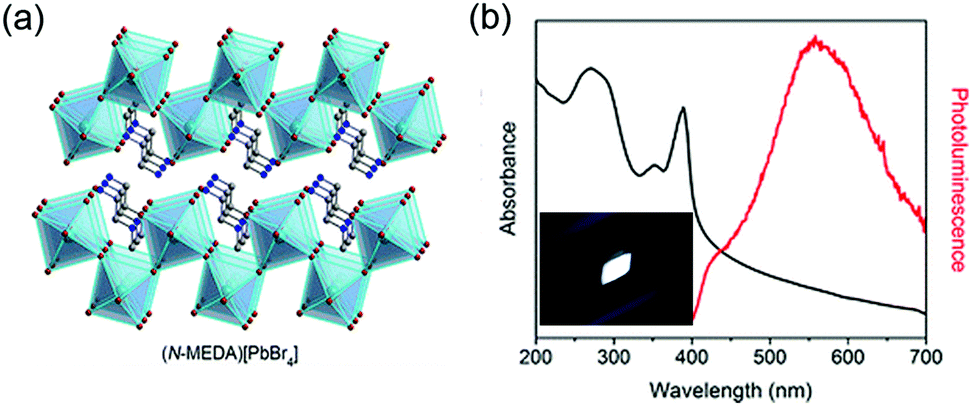 | ||
| Fig. 6 (a) Structure of <110>-oriented 2D perovskite (N-MEDA)[PbBr4] (N-MEDA = N1-methylethane-1,2-diammonium). (b) Absorption spectrum (black line) and emission spectrum (red line) for (N-MEDA)[PbBr4] with excitation at 380 nm; inset shows the luminescence of (N-MEDA)[PbBr4] powders under 380 nm UV light. Reprinted with permission from ref. 235. Copyright (2014) American Chemical Society. | ||
In the same year, Karunadasa's research group reported another family of WL-emission 2D perovskites (EDBE)PbX4 (X = Cl, Br, I, EDBE = 2,2′(ethylenedioxy)bis(ethylammonium)). The (EDBE)PbCl4 structure possess <100>-oriented inorganic sheets. Excited at 310 nm, (EDBE)PbCl4 showed two peaks. The broad emission spanned the entire visible spectrum, with the maximum at 538 nm and a FWHM of 208 nm, with a less intense shoulder peak centred at 358 nm. The PLQY of (EDBE)PbCl4 was ∼2%.236 The Br and I analogues of (EDBE)PbCl4 also show <110>-oriented inorganic layers. Upon 365 nm excitation, the Br analogue showed a WL emission with a less identifiable shoulder peak centred at 410 nm and the broad one with the maximum at 573 nm and a FWHM of 215 nm with a PLQY of ∼9%, and a CRI of 84. The CIE chromaticity coordinates were (0.39, 0.42), and it possessed a CCT of 3990 K, corresponding to “warm” WL, which makes it suitable for indoor illumination. The origin of the WL emission was the intrinsic emission of the bulk due to STE other than from extrinsic dopants or from surface defect states. The I analogue showed an observable green emission at 515 nm with a FWHM of 70 nm under 400 nm excitation with a PLQY of less than 0.5%. In 2016, Ma's group reported that upon 365 nm UV-LED chip excitation, the (EDBE)PbBr4 micro-crystal exhibited a PLQY of ∼18%.237 In 2015, Yangui et al. reported (C6H11NH3)2PbBr4 with <100>-oriented inorganic layers. The spin-coated thin film, upon 325 nm excitation, showed a very broad WL emission spanning the entire visible light range, with a peak at 2 eV, a FWHM of 660 meV and a large Stokes shift of 1.2 eV.156
In 2017, Kanatzidis's research group reported three new 2D lead bromide perovskites, and by comparing the PL emission and the structure, they found that there was a correlation between the distortion of the “PbBr6” octahedra in the 2D layer and the broadening of the PL emission. The most distorted structure with the widest light emission was observed in the most distorted <110>-oriented 3 × 3 2D lead perovskite α-(DMEN)PbBr4 (DMEN = 2-(dimethylamino)ethylamine). The FWHM was 183 nm and the lifetime was τavg = 1.39 ns. Shortly after that, the WL-emitting <100>-oriented 2D perovskite (n = 3) EA4Pb3Br10−xClx (EA = ethyl ammonium, x = 0, 2, 4, 6, 8, 9.5 and 10) was reported by the same group (Fig. 7). This had the general formula A′2An−1BnX3n+1 (A′ and A = cations; X = halide), with EA+ occupying both A′ and A sites in the system. The band gap of EA4Pb3Br10−xClx could be monotonously tuned from 3.45 eV (x = 10) to 2.75 eV (x = 0). The light emission was adjustable with the variation in X concentration and a broad-band emission was observed in EA4Pb3Cl10, while a narrow blue light emission was observed in EA4Pb3Br10, with this difference being related to the distortion levels of EA4Pb3Cl10 (large distortion) and EA4Pb3Br10 (small distortion). Among all these mixed halide compounds, EA4Pb3Br0.5Cl9.5 showed the maximum CRI of 83 and EA4Pb3Cl10 showed the minimum CRI of 66.238 Very recently, <110>-oriented 2D perovskites, C4N2H12PbX4 (X = I, Br, Cl), were reported by Kanatzidis and coworkers. The experimental band gaps follow the trend of I < Br < Cl (2.56, 3.29, 3.85 eV, respectively) and all of them showed broad-band emission.64
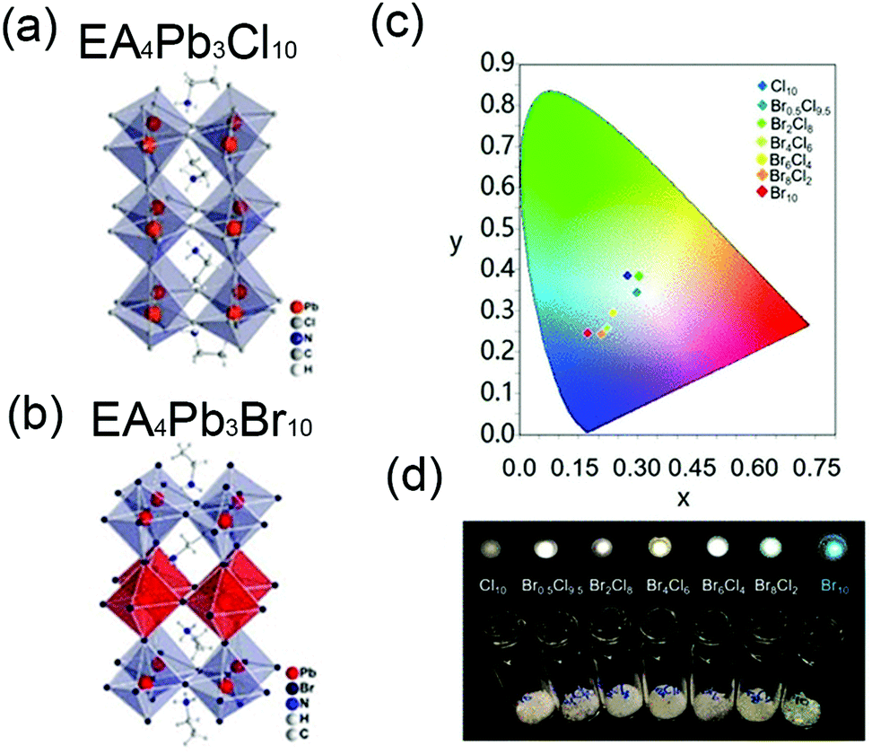 | ||
| Fig. 7 Structure of three-layered (a) EA4Pb3Cl10 and (b) EA4Pb3Br10. (c) CIE coordinates of EA4Pb3Br10−xClx (x = 0, 2, 4, 6, 8, 9.5 and 10) in 1931 colour space chromaticity diagram. WL emissions observed from EA4Pb3Br10−xClx (x = 2, 4, 6, 8, 9.5 and 10) and blue-light emission from EA4Pb3Br10 (excited at 315 nm), and (d) corresponding polycrystalline samples under UV light illumination. Reprinted with permission from ref. 238. Copyright (2017) American Chemical Society. | ||
In 2018, Wu et al. synthesized the chlorine analogue239 of (C6H13N3)PbBr4 (the first compound in which WL emission was observed).275 Upon 355 nm excitation, (C6H13N3)PbCl4 exhibited a broad-band emission with a maximum of 573 nm due to STE emission and a high-energy shoulder peak at 410 nm due to FE emission. The CIE chromaticity coordinates of this material were (0.36, 0.37) and the lifetime was estimated to be 4.416 ns. The CRI of 93 is ultrahigh and is among the highest CRI of broad-band WL-emitting hybrid perovskites. The measured PLQY was <1% and the sample was stable under ambient conditions.239 Thirumal first reported the WL emission of solution-processed 2D perovskite (C6H5C2H4NH3)2PbCl4 (with the abbreviation of PEPC) QDs. Upon 340 nm excitation, the PEPC nanoparticle solution, powder, thin film and single crystal samples all showed broad emissions ranging from ∼400 to 900 nm centred at 545 nm. It was demonstrated that the PL spectra of these samples were almost unchanged with the morphology of the materials.240 The PLQY of PEPC was low (<1%). In 2019, Gautier reported (BAPP)Pb2Br8 (BAPP = 1,4-bis(3-aminopropyl) piperazine) belonging to the <110>-oriented 2D perovskite class, with a relatively weak WL emission and a PLQY of 1.5%.233
Lead-free 2D perovskites. Cd-Based 2D hybrid perovskite with the chemical formula of (C6H11NH3)2CdBr4 exhibited WL emission under 325 nm UV light illumination, which consisted of a peak at 2.94 eV due to excitons confined in the [CdBr4]2− inorganic layer and a second peak at 2.53 eV caused by emission from the organic cations. There was a strong correlation between the structural distortion of the CdBr6 pseudo-octahedra and the broadening characteristics of the WL emission band, and also there was possible energy transfer between the inorganic and organic moieties.242 An intense PL emission was obtained in the 2D <100>-oriented (OCTAm)2SnBr4 (OCTAm = octylammonium), which showed a broad emission with a FWHM of ∼136 nm, centred at ∼600 nm and a PLQY of ∼100%.243 Its large Stokes shift of ∼250 nm and long-lived light emission of ∼3.3 μs were typical for an emission stemming from STE. This material showed high stability with no changes observed under normal humidity over 240 days at RT. By controlling the composition of this material, the luminescence could be tuned from yellow to dark red.243
B. Free exciton luminescence
Lead-containing 2D perovskites. Dou et al. studied the PL properties of (C4H9NH3)2PbBr4 (NBT = n-butylammonium), which had a <100>-oriented layered structure (Fig. 8a). Both the bulk crystal and 2D sheets with different thicknesses (22, 8 and 3 inorganic layers thick) exhibited similar intense violet-blue light emission. The bulk crystal had emission at 411 nm (2.97 eV), while the 2D sheet displayed a slightly blue-shifted peak at ∼406 nm (3.01 eV). The slight increase in the optical band gap of the ultrathin 2D sheets may be caused by lattice expansion, and this was confirmed by theoretical calculations. The PLQY of the 2D sheet was ∼26%, which was much higher than that of the bulk crystal (<1%), indicating the high quality of the single-crystal 2D sheet. The PL lifetime of the 2D sheets displayed a bi-exponential feature with lifetimes of 0.78 ns (67%) and 3.3 ns (33%).136 [(C4H9NH3)2PbI4] films showed a narrow-band emission at 517 nm with a FWHM of 25 nm, and a small Stokes shift of 4 nm due to FE emission. The absolute PLQY of this material was less than 1%.244 (N-MPDA)PbBr4 (N-MPDA = N1-methylpropane-1,3-diammonium), which also possesses <100>-oriented layers, also showed a sharp peak at 433 nm due to FE emission (Fig. 8).235
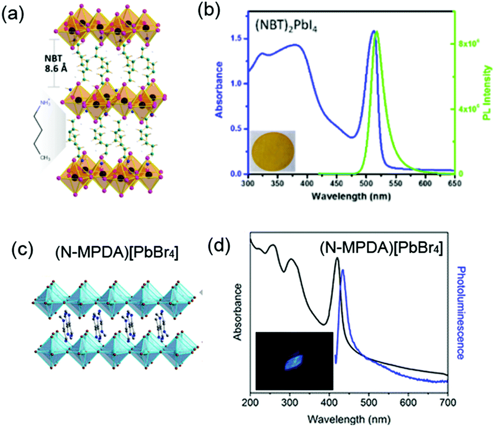 | ||
| Fig. 8 (a) Crystal structure of (C4H9NH3)2PbBr4 (NBT = n-butylammonium) consisting of <100>-oriented layers. (b) Steady-state absorption (blue) and photoluminescence (green) of (NBT)2PbI4. The insets show orange emission from (NBT)2PbI4 under UV light illumination. Reprinted with permission from ref. 136. Copyright (2014) American Chemical Society. (c) Crystal structure of the <100>-oriented (N-MPDA)[PbBr4] (N-MPDA = N-methylpropane-1,3-diammonium). (d) Absorption spectrum (black) and emission spectrum (blue) under excitation at 400 nm for (N-MPDA)[PbBr4]. The inset shows the luminescence from powders of (N-MPDA)[PbBr4] under 380 nm irradiation. Reprinted with permission from ref. 235. Copyright (2014) American Chemical Society. | ||
(C4H12N)4Pb3I4Br6 is a <100>-oriented 2D perovskite with n = 3. Optical transmission measurements on (C4H12N)4Pb3I4Br6 film showed two absorption bands centred at 474 and 508 nm. This compound showed a strong green luminescence emission centred at ∼519 nm, with a FWHM of ∼60 nm. The Stokes shift between the absorption at 508 nm and emission at 519 nm was quite small at ∼11 nm. Thus, the luminescence originated from FE.241
Lead-free 2D perovskites. (C4H9NH3)2EuI4, reported by Mitzi et al., is the only known example of an f-block metal-based 2D hybrid perovskite, and it displayed strong blue PL centred at 460 nm.
4.1.2.2. 1D and 0D perovskites. Lead-containing 1D perovskites: The structure of (H2O)(C6H8N3)2Pb2Br10 (abbreviated to PzPbBr) consists of twisted corner-sharing metal halide octahedra forming 1D twisted chains two octahedral units wide. It exhibited intense yellow-white emission under 365 nm excitation. The optical characterization of PzPbBr showed a strong Stokes shift and a broad PL emission band peaking at 580 nm with a PLQY of ∼9%.296
Lead-free 0D perovskites: Cs4SnBr6 featuring a 0D structure with separated SnBr6 octahedra exhibits broad PL with a central wavelength of 540 nm and a PLQY of 15.5%, which is attributed to STE emission. The Stokes shift and the STE emission band can be tuned from 500 nm to 620 nm by cationic or anionic mixing following the general formula Cs4−xAxSn(Br1−yIy)6 (A = Rb, K; x ≤ 1, y ≤ 1).69 The structure of the tin chloride of 3,3 0-diaminodiphenyl sulfone (C12H14N2O2S)[SnCl6]H2O (abbreviated as (AMPS)[SnCl6]H2O) consists of isolated [SnCl6] octahedra surrounded by organic (AMPS) cations. It showed strong quasi-WL emission that could be observed by the naked eye, even at RT. Wherein (AMPS) molecules act as donors and [SnCl6] molecules act as receptors, the PL spectrum consists mainly of two bands, a wide and strong band centred at 592 nm and a shoulder peak with the maximum at 482 nm. The strong peak at 592 nm was associated with light-induced exciton formed in the inorganic SnCl6 octahedra, while the shoulder peak was designated as π–π* transition in the AMPS organic cation.249 The 0D mixed metal halide perovskite (C8NH12)4Bi0.57Sb0.43Br7·H2O contains [BiBr6]3 and [SbBr6]3 octahedra and showed an experimental band gap of 2.80 eV. The crystal showed an ultra-wide band emission ranging from 400 to 850 nm, with a PLQY of 4.5%, which came from both FE and STE. Meanwhile, (C8NH12)4BiBr7·H2O showed a narrow emission at 450 nm, which is close to the exciton absorption peak (400 nm), so it belongs to FE emission with a PLQY of 0.7%, demonstrating that the mixed B-site perovskite not only has good ambient stability but also good photostability.251 A film of the 0D methylammonium iodonium (CH3NH3)3Bi2I9 perovskite exhibited a wide band gap of 2.9 eV, and PL emission was observed at 1.65 eV (751 nm) under 488 nm optical excitation.250 In 2018, Ma's group reported a 0D (C4N2H14Br)4SnBr6 with a PLQY of ∼95%, and (C4N2H14I)4SnI6 with a PLQY of ∼75%.252 By mixing with a halide, a yellow emission centered at 582 nm, and a FWHM of 126 nm at RT were observed from (C4N2H14Br)4SnBrxI6−x (x = 3). The highest PLQY oberserved was ∼85%. The colour index of a UV-pumped WLED, prepared by using this material and BaMgAl10O17:Eu2+ as a blue phosphor, was as high as ∼85.253 All these values of Sn-based OIHPs reported by Ma's group are among the highest PLQYs of STE luminescence reported so far.
Perovskite-like halides with 1D structures. The structure of (C9H10N2)PbCl4 (3-aminoquinoline abbreviated as AQ) consists of chains of edge-sharing PbCl6 octahedra extending along the b-axis. This compound showed a strong yellow WL emission, consisting of a yellow broad-band centred at 538 nm and a narrower UV band centred at 340 nm. The wide yellow band was related to the π–π* transition inside the organic molecule, while the UV emission was attributed to the Wannier excitons confined in the inorganic lines.259
Chains of [PbX42−]∞ formed by edge-sharing PbX6 octahedra with organic moieties surrounding show broad emission, such as C4N2H14PbBr4,258 C5H14N2PbCl4·H2O260 and (TDMP)PbBr4 (TDMP = trans-2,5-dimethylpiperazinium).233 Among these, (TDMP)PbBr4 (TDMP = trans-2,5-dimethylpiperazinium) exhibited intense WL emission with a PLQY of 45% and high CRI of 75. The emission originated from STEs through the colour centres, such as Pb23+, Pb3+, X2 and X2− (X = halide).244
The structure of (HMTA)3Pb2Br7 (HMTA = C6H13N4+) features six face-sharing metal halide dimers (Pb2Br95−) joined at the corners to form a ring extending in one dimension. The inner and outer surfaces of the tube are surrounded by HMTA (HMTA)3Pb2Br7, which can be excited by ultraviolet light ranging from 250 to 400 nm to produce a broad emission peak ranging from 450 to 750 nm centred at 580 nm, with a large FWHM of 158 nm. The 1D compound (2,6-dmpz)3Pb2Br10 (2,6-dmpz = 2,6-dimethylpiperazine) with corner- and edge-sharing octahedra forming chains exhibited a band gap of 2.49 eV, and displayed a broad-band light emission centred at 2.12 eV with a FWHM of 325 meV and average life time of 23.03 ns. Its CIE was (0.44, 0.46) and the CRI was 77. It had the highest PLQY of 12%, owing to its unique structure, which allowed efficient charge carrier relaxation and light emission.37
Perovskite-like halides with 0D structures. The 0D (C9NH20)6Pb3Br12 contains face-sharing PbBr6 trimer clusters, which are connected by the organic cations.264 A broad-band green PL peaking at about 522 nm with a FWHM of 134 nm was observed. The CIE chromaticity coordinates were determined to be (0.264, 0.392) and the PLQY was around 12%.264
Other compounds. In addition, several sulfonium Pb–Br hybrids were reported showing broad-band visible light emission, such as (tms)4Pb3Br10 (tms = trimethylsulfonium; (CH3)3S+) and (tmpa)4Pb3Br10 (tmpa = trimethylphenylammonium).256 Abid et al. reported (C7H12N2S)2PbBr3 abbreviated as (ABT)2PbBr3. The structure consisted of an infinite double-chain constructed by edge-sharing PbBr6 octahedra. Under UV emission, this material exhibited WL emission with an intensity that can be seen with the naked eye. Its PL spectrum was characterized by a broad emission band covering the visible spectrum, consisting of blue, green, yellow and red components at 450, 475, 530 and 580 nm, respectively. PL measurements with various excitations showed that the WL emission only occurred within a narrow excitation range of about 394 nm.263 The structure of (1,4-bbdms)3Pb3Br12 (1,4-bbdms = (CH3)2S(CH2)4S(CH3)22+) consists of isolated trimers and pentamers of face-sharing octahedra.256 It exhibited broad red PL centered at 690 nm and two higher-energy and lower-intensity PL bands at ca. 375 and 460 nm, which could be attributed to emission from FEs or defects.
4.2. Rare-earth-doped perovskites
Host materials with a perovskite structure have a considerable degree of structural flexibility to accommodate a variety of activating and sensitizing cations. Early in 1967, Yamamoto et al. started to research the luminescence of trivalent rare-earth elements (Eu3+, Tb3+ and Pr3+) in the perovskites SrTiO3 and BaTiO3.297 Generally, the characteristics of doped trivalent rare-earth elements are preserved in perovskite structures. For example, upon UV and low voltage cathode-ray excitation, LaInO3:Sm3+, LaInO3:Pr3+ and LaInO3:Tb3+ phosphors prepared by a sol–gel process showed strong orange–red, blue–green and green luminescence, respectively.298 High-throughput combinatorial methods for synthesizing and characterizing oxide perovskites have been developed to identify and optimize interesting new materials.299,300 The functioning of oxide perovskites can in different material dimensionalities. Meanwhile, it is interesting to note that metal oxide nanosheets could be synthesized by the exfoliation of bulk layered oxides. For example, Ida et al. succeeded in the exfoliation of Bi2SrTa2O9 to obtain a mono-nanosheet of 1.3 nm thickness with blue emission.301 By doping Eu3+ or Tb3+ into perovskite nanosheets prepared by the exfoliation of single- or double-layered perovskite oxides, such as K2Ln2Ti3O10, KLnNb2O7 and RbLnTa2O7 (Ln: lanthanide ion), intense red and green emission could be observed under UV illumination.302 The visible emission results from energy transfer within the nanosheet, also considering the overlap between the excitation spectrum and the band gap absorbance.Ce. Allowed 5d–4f transitions of lanthanide ions (e.g. Ce3+, Eu2+) have short decay times (<1 ms) and have been very successfully utilized for scintillators.303 Scintillators are used to detect ionizing radiation. Cerium-doped lanthanide perovskites, such as YAlO3(YAP:Ce3+) and LuAlO3(LuAP:Ce3+), are used as scintillators as they exhibit fast scintillation and a high light yield.90,91,304 The excitation spectrum usually has a maximum intensity at the fundamental absorption edge comparable with that from direct 4f–5d excitation. The free excitions are able to migrate along a long distance and transfer their energy to luminescence centres. This process is very efficient in the excitation energy region, since the capture of a hole by Ce3+ is favourable considering the fact that cerium is more stable in the tetravalent state.304 YAP:Ce shows a broad emission band due to the presence of Ce ions.305 Five bands could be clearly distinguished in the excitation spectrum because of the complete splitting of the 5d excited state level at a low Y3+ site symmetry.306
Pr. The optical properties of Pr3+-doped titanates with a perovskite structure are influenced by the semiconducting nature of the host. In CaTiO3:Pr3+, the excitation of the red luminescence is achieved through the conduction band states and then transferred to the emitting level of Pr3+.307 In this process, electron–hole pairs are produced via O(2p)–Ti(3d)–Pr(4f). Meanwhile, the emission enhancement of Pr3+ due to charge compensation depends on the compensator types, because the hole capture cross-section is strongly affected by the compensator. For host materials, the intensities of the red luminescence due to the f–f transitions of Pr3+ ions increase in the order of cubic SrTiO3, tetragonal BaTiO3 and orthorhombic CaTiO3.308 The increase in f–f transition probability is caused by the point symmetry lowering, which can be controlled by either crystallographic site symmetry or the solid-solution effect at the alkaline-earth site. In the ATiO3 (A = Pb, Ca, Ba, Sr) perovskite-type amorphous thin films, a tail is observed in the absorbance spectrum curve.309 Usually, the optical properties of amorphous semiconductor compounds are characterized by the presence in the plot of photon energy versus the optical absorption of a tail, in which the optical absorption falls almost asymptotically to zero. This region is normally transparent in crystalline solids.310 The tail in the absorbance spectrum curve is caused by the delocalized electronic levels of the fivefold coordination through the displacement of O. The radiationless relaxation pathways lead to the quenching of 3P0 emission and subsequently to the typical single red luminescence from the 1D2 level in CaTiO3:Pr3+.311 STEs participate in the relaxation process and the Pr3+/Ti4+ ↔ Pr4+/Ti3+ charge-transfer state (CTS) is proposed as the final relaxation channel to the emitting 1D2 level. The difference between the luminescence properties of CaTiO3:Pr3+ and CaZrO3:Pr3+ could be explained by the relaxation pathway. The low-lying Pr3+/Ti4+ ↔ Pr4+/Ti3+ charge-transfer state is the final radiationless relaxation pathway to the emitting 1D2 level in Pr3+-doped CaTiO3, instead of the low-positioned 4f–5d band. In the zirconate, the relative high stability of the tetravalent state of zirconium is not in favour of a low-lying intervalence charge-transfer state and therefore, when excited in the conduction band at 254 nm, CaZrO3:Pr3+ shows prominent greenish-blue luminescence from the 3P0 level instead of a single red emission from the 1D2 level. The emission profile of praseodymium-doped lanthanum hafnate, La2Hf2O7:Pr3+, displayed the involvement of both the 3P0 and 1D2 states, because the Pr3+ ions occupy both the Hf4+ sites and La3+ sites.312 Pan et al. noticed persistent luminescence in crystalline CaTiO3:Pr3+ nanoparticles prepared from a complex polymer precursor.313 The 612 nm red-emitting persistent luminescence of Ca3Ti2O7:Pr3+ can be activated by multiple charge-transfer processes. The red afterglow can last for ∼5 min, with the trap-depth exponentially distributed at 0.69–0.92 eV.314
Sm. The reddish-orange emission of Sm3+ is caused by transitions from 4G5/2 to 6HJ (J = 5/2, 7/2, 9/2, 11/2).315 Sm3+-doped Srn+1SnnO3n+1 (n = 1, 2, ∞) is a good example to elucide the effects of the crystal structure dimensionality on the luminescent properties.114 The mechanoluminescence enhancement process is related to the 2D layered structure and the charge-transfer process. The intensity of mechanoluminescence for Sr3Sn2O7:Sm3+ is three orders of magnitude higher than that for SrSnO3:Sm3+ due to the effective confinement of transfer energy in the 2D layer. The band gaps of Sr2SnO4, Sr3Sn2O7 and SrSnO3 decrease as 4.43 eV (280 nm), 4.13 eV (300 nm) and 3.88 eV (320 nm), in accordance with the change in the crystal structure dimensionality. This means that in SrSnO3 with a 3D connecting octahedral network, the charge-transfer process occurs more easily. The band gap of Sr3Sn2O7:Sm3+ could be further tailored by Si or Ge substitution. The more electronegative Si and Ge makes the charge transfer occur more easily and reduces the band gap.108
Eu. The luminescence of Eu3+ originates from the intra-configurational 5D0–7FJ transitions. The emission spectra of CaSnO3:Eu3+ and BaSnO3:Eu3+ are dominated by the red 5D0 → 7F2 transition at 614 nm.316 The onset of the excitation spectra of MSnO3 (M = Ca, Sr and Ba) at 77 K occur at almost the same position as for the UV-VIS absorption spectra shown, which indicates that the emission from MSnO3 is derived from band gap excitation.317 The PL spectra were red-shifted from CaSnO3 to SrSnO3 to BaSnO3, as observed in their diffuse reflectance spectra. Eu3+-Doped perovskite nanosheets of the form La0.90Eu0.05Nb2O7 were prepared by the soft chemical exfoliation reaction of K1−xHxLa0.90Eu0.05Nb2O7 with a tetrabuthylammonium hydroxide aqueous solution.318 The resulting colloidal La0.90Eu0.05Nb2O7 nanosheet suspension exhibited a photoluminescence emission from the 5D0 to 7FJ manifold transitions of Eu3+ by either a direct excitation of Eu3+ or by host excitation, whereas no host emission was observed at room temperature. In the case of the bulk precursors K1−xHxLa0.90Eu0.05Nb2O7, the direct excitation yields more intense emission than the host excitation. On the contrary, the most intense emission from the La0.90Eu0.05Nb2O7 nanosheets was observed by exciting at the broad excitation band maximum (353 nm). The difference in the photoluminescence properties between the La0.90Eu0.05Nb2O7 nanosheets and their bulk precursors seems to be related to the dimensionality of these host structures and the confinement of the energy-transfer process between the host layer units and the Eu3+ activators. Photoluminescence studies into Eu3+-doped double perovskites with the formula A2CaWO6 (A = Sr, Ba) have revealed that the forced electric dipole (ED) transition is present when Eu3+ is substituted at the non-centrosymmetric Sr-site. Substitution at the centrosymmetric Ca-site shows both ED and magnetic dipole (MD) transition.319 In A- and B-site substituted double-perovskite Sr2CaMoO6 doped by Eu3+, the photoluminescence intensity of the B-site substituted Sr2CaMoO6 is evidently higher than that of the A-site substituted phosphor.320 In different hosts, the location of the CT bands of Eu3+ is also different, centred at 270, 250 and 263 nm, corresponding to CaZrO3:1%Eu,SrZrO3:1%Eu and BaZrO3:1%Eu.321 Powdered samples of the perovskite BaSnO3 exhibit strong near-infrared (NIR) luminescence at room temperature following band-gap excitation at 380 nm (3.26 eV).322 The emission spectrum is characterized by a broad band centered at 905 nm (1.4 eV), tailing on the high-energy side to approximately 760 nm. The luminescence involves a defect state. As the strontium content increases, the excitation maximum and band gap shift further into the UV range, while the intensity of the NIR emission peak decreases and is shifted further into the infrared. This combination leads to an unexpectedly large increase in the Stokes shift. The unusual NIR PL in BaSnO3 may originate from recombination of a photogenerated valence-band hole and an occupied donor level, probably associated with a Sn2+ ion. It was found that the PL intensity of the phosphor NaY0.7Eu0.3TiO4 is about three times higher than that of the phosphor NaGd0.7Eu0.3TiO4 with the optimal composition. This may be due to the larger distortion from the doping of Eu3+ in the former compound NaYTiO4 than that in the latter NaGdTiO4 lattice, based on the large difference in ionic radii.323 Recently, Bala predicted the blue emission (2.48–2.85 eV) of the Eu2+-doped CsPbBr3 perovskite by first-principle calculations. The results showed that Eu2+ doping is favourable because of the energetic stablility in the CsPbBr3 perovskite host with negligible strain. Therefore, further research on Eu2+-doped all-inorganic halide perovskites is expected.324
Tb. The luminescence of Tb3+ could be caused by energy transfer. In the Gd3+–Tb3+-activated LaAlGe2O7, the decay time of Tb3+ emission under Gd3+ excitation at the 6IJ energy level was longer than that under direct Tb3+ excitation at the 5L10 energy level, which reinforces the view of the existence of effective Gd3+-to-Tb3+ energy transfer.325 However, the presence of a broad host emission (green, 544 nm) along with strong Tb3+ emission (587 and 622 nm) indicates incomplete energy transfer from the host to Tb3+ in Tb3+-doped SrZrO3.326 DFT calculations showed an energy mismatch of the Tb-d states with the Zr-d and O-p states, which explains the difficult energy transfer from the SrZrO3 host to the Tb3+ ion.
Er. The upconversion photoluminescence of the Er3+-doped perovskite ABO3 structure has been widely studied. In Er3+-doped BaTiO3, Er3+ occupying the B-site strongly enhances the 4S3/2–4I15/2 emissions due to the thermal quenching and lower symmetry induced by the phase transition. The 2H11/2 state is thermally quenched to the 4S3/2 state and subsequently contributes to the enhanced population of the 4S3/2 state. The crystal field formed by the octahedral oxygen ions with a lower symmetry than Oh is more suitable for the Er intra-4f transitions.327
Yb. Yb3+-Doped luminescent perovskites have mainly been investigated for the quantum cutting effect, for which two near-infrared photons are emitted for each absorbed visible photon. Besides this, luminescence due to charge transfer is also possible. For YAlO3 doped with 2% Yb3+, the broad emission bands with maxima at 360 and 533 nm are assigned to CT transitions of Yb3+, accompanied by a narrow 2F5/2 → 2F7/2 emission band peaking at about 1000 nm.183 NIR emission has also been observed in Yb3+-doped halide perovskite CsPbX3 NCs328 Yb3+ ions occupy the Pb2+ crystallographic sites in CsPbCl3 NCs.329 Near-infrared PLQYs of 170% have been measured for Yb3+:CsPbCl3 NCs. Kroupa et al. reported Yb3+-doped CsPb(Cl1–xBrx)3 films with extremely high quantum yields reaching over 190%.330 The extremely efficient sensitization of Yb3+ luminescence in CsPbCl3 NCs is due to the Pb atom with STE, which acts as the energy donor in a quantum cutting process.331 In the Yb3+-doped double perovskites Cs2AgInCl6 and Cs2AgBiX6 (X = Cl−, Br−), the characteristic f–f transition emissions of Yb3+ are also observed due to an energy transfer from the hosts to the 2F5/2 state of the Yb3+ ion.332,333
4.3. Transition metal-doped perovskites
Cr. Generally, the luminescence of octahedral Cr3+ complexes is in the form of sharp lines from the 2Eg state. However, broad-band near-infrared emission from the 4T2g state can be observed, either alone or in combination with the 2Eg lines, in weak crystal fields provided by ligands CI−, Br− and I−, such as Cs2NaMX6 (M = In, Y; X = CI,Br).334 For Mn4+, the ground state electronic configuration is 3d3, isoelectronic with that of Cr3+. As a result, they share similar luminescence, which consists of a sharp zero-phonon line and an accompanying vibronic sideband emission. The lowest excited state is 2E, and the excitation is usually dominated by O2− to Cr3+/Mn4+ charge-transfer transition. Katayama et al. reported the deep-red persistent luminescence of Cr3+. The LaAlO3:Cr3+ sample showed persistent luminescence peaking at a very long wavelength of 734 nm due to a Cr3+:2E → 4A2 transition after ultraviolet excitation. The Sm3+ ion was found to be a good codopant for increasing the persistent luminescence intensity by more than 35-fold. The Cr3+–Sm3+-codoped LaAlO3 sample with peak luminescence at 694 nm is a candidate phosphor for in vivo imaging application.335Mn. The photoluminescence properties of Mn4+-activated perovskites have been reported in a series of oxide phosphors, including germinates, silicates and aluminates. According to Adachi,336 they could be classified into three groups according to their different PL spectral features. The first type reveals a zero-phonon line (ZPL) emission peak due to the 2Eg → 4A2g transitions in the Mn4+ ion together with the Stokes and anti-Stokes sideband peaks. However, the second-type of phosphors promise no clear identification of the ZPL emission peaks, even in the PL spectra measured at cryogenic temperatures. The ZPL emission peaks in the third type of phosphors can be tentatively determined from an analysis of the PL spectra using a characteristic Poisson function. The ZPL absorption transition energies in the PL excitation spectra are determined by performing a Franck–Condon analysis within the configurational-coordinate (CC) model. These transition energies and ZPL emission energies are used to obtain the crystal field (Dq) and Racah parameters (B and C) of the Mn4+ ions in these Mn4+-activated oxide phosphors. In Gd2MgTiO6:Mn4+, under 315 nm excitation, the sample exhibited a strong zero-phonon line located at 681 nm together with broad sidebands around 700 nm.102 Brik et al. adopted the crystal structure data and the overlap integrals between the Mn4+ and O2− ions to demonstrate that, despite the increasing Mn4+–O2− interatomic distance, the exchange charge contribution to the total values of CFP (which is proportional to the above-mentioned overlap integrals) increased from Y2Ti2O7 to Y2Sn2O7.337 This increased overlap in Y2Sn2O7 occurs despite the fact that the Mn4+–O2− bond distance in Y2Sn2O7 is longer than in Y2Ti2O7 and is attributed to a lack of hybridization (covalent bonding) between the filled 2p orbital of the oxygen ion occupying the 48f site of the pyrochlore lattice and the filled Sn4+ 4d10 orbital. In the Mn4+-doped double perovskites La2LiSbO6 and La2MgTiO6, the 2Eg → 4A2g emission transition was determined by octahedral site distortion. The greater the site distortion, the lower the Mn–O covalent interaction and the higher the energy of the 2Eg → 4A2g emission transition.338 The double perovstkite-type La2MgGeO6:Mn4+ exhibited deep-red emission peaking at 708 nm under UV irradiation. It also exhibited NIR persistent luminescence in the range from 670 nm to 720 nm, lasting for 60 min.339 The after-glow behaviour is dependent on the host intrinsic defects, and could be enhanced by the incorporation of Al3+ ions. The double-perovskite Ba2GdSbO6:Mn4+ phosphor demonstrated strong red emission, ascribed to a spin-forbidden Mn4+:2Eg → 4A2g transition in the region of 620–750 nm. Zhong et al. discovered that Li+, Mg2+, Zn2+, Si4+, Ti4+ and Ge4+ dopants are beneficial for enhancing Mn4+ luminescence.340
Phosphors with Mn2+ as the activator usually have a relatively long lifetime in the order of milliseconds due to the spin-forbidden 4T1–6A1 transition. At higher Mn2+ concentrations, a red spectral shift and an increase in the oscillator strength have been observed,341 which were not simply caused by concentration quenching. Ronda and Amrein proved that the relaxation of the spin-selection rule and the spectral red-shift stem from the spin exchange interaction upon going from isolated Mn2+ ions to Mn2+ ion pairs. Recently, Pradhan presented a review on a brief history of the development of luminescent Mn-doped NCs over the last 25 years and summarized the important findings and future prospects.342 The typical colour, spectra and energy levels can be found in Fig. 9.
 | ||
| Fig. 9 (a) Photograph of CsPbCl3 and Mn-doped CsPbCl3 under 365 nm excitation. (b) Normalized temperature-dependent emission spectra of Y2MgTiO6:0.2%Mn4+ under 355 nm excitation. Crystal structure of the Y2MgTiO6:0.2%Mn4+ double perovskite. Temperature-dependent decay curves of the 698 nm emission in Y2MgTiO6:0.2%Mn4+ under a 355 nm pulsed YAG:Nd laser. (c) Energy level diagram for the Mn2+ emitting centre in a free-ion state and in a crystal field of cubic symmetry, energy band structure of CsPb(Cl/Br)3 PQDs (Br/Cl ratio gradually increases from left to right), and energy transfer mechanisms from PQDs to Mn2+ dopants. (d) Multicolour emissions of a series of silica-coated PQD phosphors under the excitation of a UV lamp (from left to right: CsPb(Cl0.4Br0.6)3, CsPbBr3, CsPb0.835Mn0.165Cl3, CsPb0.835Mn0.165(Cl0.6Br0.4)3, CsPb0.835Mn0.165(Cl0.5Br0.5)3, CsPb0.835Mn0.165(Cl0.4Br0.6)3, CsPb0.835Mn0.165(Cl0.3Br0.7)3, and CsPb0.835Mn0.165(Cl0.05Br0.95)3). (e) Absorbance (dashed lines) and PL (solid lines) spectra of CsPbCl3. Panels adapted from: a, b reprinted with permission from ref. 281. Copyright (2019) American Chemical Society; c and d reprinted with permission from ref. 350. Copyright (2017) American Chemical Society; e reprinted with permission from ref. 328. Copyright (2018) American Chemical Society. | ||
Mn2+-Doped cesium lead halide (CsPbX3) perovskite NCs exhibit a broad luminescence, attributed to the spin-forbidden ligand field transition (4T1–6A1) of Mn2+ ions at ∼600 nm, together with the exciton luminescence of the host.343 The d–d transition of Mn2+ ions results from exciton-to-Mn energy transfer, indicating a strong exchange coupling between the charge carriers of the host and the dopant d electrons.281,344 The exciton–dopant energy transfer occurs in the time range of 50–100 ps, slower than the trapping of carriers in the host lattice, which takes 8–10 s. By varying the doping content, the Mn2+ luminescence could be tuned from 585–625 nm.345 According to Xu et al., the doping level of Mn2+ in CsPbCl3 could reach 25% of the Pb content, with no substantial change in the morphology of the NCs.346 The emission intensity could be greatly enhanced by the further growth of an undoped shell. A CsMnCl3 phase with complete Mn dopant substitution by spinodal decomposition was realized by Li et al.347 It had a shorter Mn lifetime, which was consistent with the short Mn–Mn distance within the CsMnCl3 phase. A single-exponential decay was detected for a low concentration of Mn2+, with a concentration-independent lifetime of 1.8 ms. At a high doping level, the shorter and multiexponential decay becomes concentration dependent, reflecting the energy migration from Mn2+–Mn2+ dimers to traps.348
Mn-Doped CsPbCl3 could be converted to Mn-doped CsPbBr3 through an anion exchange reaction, but only weak Mn luminescence was obtained in Mn-doped CsPbBr3.278,349 To overcome the reabsorption and anioin-exchange effect in the mixing of multiple perovskite quantum dots, silica-coating was proposed to improve the air stability and suppress the anion-exchange.350 Parobek et al. managed to synthesize Mn-doped CsPbBr3 NCs with an intermediate structure (L2[Pb1–xMnx]Br4, L = ligand).351 Qiao et al. reported a photoinduced synthesis of Mn-doped CsPbX3 (X = Cl, Br). The mild nature of the method preserved the size and anisotropic morphology of the NCs.352 The trapped nonradiative energy could be recycled by doped Mn according to Wei et al., who observed the doped Mn snatching energy from the non-radiative trap states rather than from band states.353 Mir observed that by controlling the size and shape of Mn-doped CsPbBr3, the intensity of Mn emission decreases with the optical band gap of the host decreasing from 2.92 to 2.53 eV. The quenching of Mn emission was mainly caused by the back energy transfer from Mn to the host.354 Chen et al. introduced a dimethyl sulfoxide (DMSO)–MnBr2/PbX2 composite as a precursor for the room-temperature facile synthesis of Mn-doped CsPbX3 (X = Br, Cl) NCs. By adjusting the PbBr2/PbCl2 ratio, the excitonic emission spectra could be tuned from 517 nm to 418 nm.279 The temperature-dependent spectral properties of the pure and Mn-doped CsPbCl3 NCs revealed that the Mn luminescence was enhanced at 78–270 K, because more carriers located at the excitonic state could transit directly to the thermally excited 4T1 energy level of Mn due to the increased thermal perturbations (kBT). Higher temperatures reduce the number of carriers located in the excitonic state, and therefore the Mn PL intensity decreases gradually.355 Besides Pb-halide peroskites, non-toxic metal halide double perovskites, such as Cs2AgInCl6, have been reported as a host to accommodate Mn2+.356
Near-infrared upconversion emission could be observed in high Mn2+ doping of KZnF3:Yb3+, Mn2+ NCs.357 The 770 nm peaked emission originated from the 6A1g(S)4T1g(G) → 6A1g(S)6A1g(S) transitions of the Mn2+–Mn2+ dimers.
Ni. Broadband near-infrared photoluminescence could be obtained by exciting KMgF3:Ni2+ using an 808 nm laser diode. The emission peak was centred at 1624 nm with a FWHM larger than 315 nm, originating from the 3T2g(3F) → 3A2g(3F) electronic transition of the octahedrally coordinated Ni2+. The emission range covered the wide absorption spectrum of typical combustion products, which makes KMgF3:Ni2+ useful for combustion gas sensors358
Both monovalent and divalent Cu cations have been doped into perovskite compounds.87 However, the presence of Cu2+ just improves the thermal stability and the optical performance of CsPb1–xCux(Br/Cl)3 NCs, without changing the blue excitonic luminescence.359
4.4. Bi-Doped perovskites
Zhou et al. employed a low-temperature (∼350 °C) ion exchange approach to synthesize (K,Na)La1–xTa2O7:xBi3+ with RbLa1–xTa2O7:xBi3+ as precursors.115 The 2D-layered perovskite doped with Bi3+ exhibited yellow emission due to the transitions from the excited state 3P1 or 3P0 to the ground state 1S0. Lozhkina et al. argued that although the optical absorption of both the single-crystal and powder samples of CsPbBr3 doped with Bi presented a red-shift, the band gap of Bi-doped perovskite remained unchanged, according to low-temperature photoluminescence studies.360 The valence band structure was also not changed upon doping Bi3+, and only the Fermi level was increased by 0.6 eV, which suggests the formation of electron-type defect states localized closer to the bottom of the conduction band. In double-perovskite Cs2AgInCl6, the band gap decreased from 4.25 to 3.28 eV upon 1% Bi2+ doping, together with a broad band emission peak at 580 nm.3614.5. Strategies for PLQY and chemical stability improvement
Phosphors for LEDs need to be thermally stable due to the possible high working temperatures of devices. The stability of perovskite QDs need to be further improved because they tend to aggregate and surface oxidation occurs at high temperatures due to incomplete surface passivation.362 The methods for stablity improvement are summarized in this section.Encapsulation. Wang et al. prevented the anion-exchange effect by mixing perovskite CsPbBr3 NCs with mesoporous silica particles to form nanocomposites. The green emissive mesoporous silica nanocomposites could be mixed with red perovskite NCs to fabricate an LED without the anion-exchange effect.363 Embedding CsPbBr3 NCs into robust and air-stable rhombic prism Cs4PbBr6 microcrystals enabled a high emission efficiency in the solid state. The lattice matching contributed to the improved passivation.364 Wei et al. packed CsPbBr3 NCs into crosslinked polystyrene beads via a simple swelling–shrinking strategy in nonpolar toluene and hexane. The prepared composite beads retained superior water-resistance, still emitting strong luminescence after 9 months water immersion.365 CsPbBr3 quantum dots incorporated into a silica/alumina monolith exhibited high photostability under the strong illumination of blue light for 300 h due to a robust protective layer of compact SiO2 and Al2O3 against oxygen and moisture.366,367 Incorporation of perovskite NCs into a polymeric matrix is an effective strategy to improve the water resistance and to prevent anion exchange between different halide NCs in the solid state. This can be performed by mixing pre-synthesized perovskite NCs into a polymer matrix or by the in situ fabrication of perovskite NCs-embedded composite films. Meyns et al. coated CsPbX3 NCs with poly(maleic anhydride-alt-1-octadecene) (PMA) to improve the stability as well as the processability.368 Zhang et al. embedded CsPbX3 NCs into microhemispheres of a polystyrene matrix to improve the hydrolysis resistance.369 Antisolvent vapour treatment of CsPbBr3 embedded in a dielectric polymer matrix of polyethylene oxide (PEO) resulted in a lower trap state density because of the larger crystal size and the fewer grain boundaries, which boosted the luminescent efficiency and the stability of perovskite LEDs.370 Zhu et al. embedded green-light-emitting CsPbBr3 and red-light-emitting CsPb(Br/I)3 NCs into carboxyl-containing polymethyl methacrylate (PMMA) by a hot-injection method to improve the efficiency and stability.371 By introducing Cs+ as a dopant and 3,3-diphenylpropyamine (DPPA) as a capping ligand, the compatibility between NCs and the polymer was improved by decreasing the solubility variance of the precursors. With this method, the PLQY of red-emissive MAPbI3 was increased from less than 15% to 91%.218 Embedding CsPbX3 (X = Cl, Br, I) perovskite NCs in the cage of zeolite-Y significantly improved its temperature and water resistance.372 Xu et al. formed air-stable CsPbBr3 nanoplatelets in the matrix of Cs4PbBr6 nanosheets by reducing the thickness of Cs4PbBr6 to ∼7.6 nm, which is at the scale of the exciton Bohr radius of CsPbBr3.373 Hydrophobic solid paraffin could be used to encapsulate all-inorganic NCs to form water-stable composites. Meanwhile, the anioin exchange, which causes undesirable spectral changes, could be simultaneouly inhibited for the isolation of the NCs by a solid paraffin layer.374 He et al. loaded perovskite NCs in a host–guest metal–organic framework (MOF) forming ZJU-28⊃MAPbBr3, and found this could significantly diminishes the aggregation, provide effective surface passivation and shelter the NCs from the environment.375 Integrating CsPbBr3 into MOFs also improves the stability of the NCs as the QDs are encapsulated in a porous zeolite matrix. The CsPbBr3 @Uio-67 composite376 and CsPbX3-zeolite-Y composite exhibited stable photoluminescence properties under ambient atmospheric conditions.377
Synthesis atmosphere. Motti et al. discovered that the band-to-band radiative emission can be quenched for lead halide perovskites films in an inert environment, independently of the chemical composition. However, this negative effect could be compensated by the presence of oxygen, even in a very small amount.378 Similarly, Brenes et al. investigated the impact of the atmosphere on the local luminescence of MAPbI3 perovskite grains using confocal photoluminescence measurements.379 The results showed that the emission from each grain depends sensitively on both the environment and the bright/dark nature of the specific grain. In the presence of oxygen and/or water molecules, the dark grains show a substantial improvement in emission, while the bright grain emission stays the same. However, the luminescence detoriates in nitrogen or under vacuum conditions. It is possible that moisture forms a passivating shell on the surfaces of the grains, converting the vacancies on the surfaces to amorphous species. Brenes showed that methylammonium lead iodide (MAPbI3) polycrystalline perovskite films treated with combined treatments of light and atmosphere exhibit properties comparable with perovskite single crystals.380
Doping engineering. The substitution of Mn2+ has been demonstrated to be an effective strategy to fundamentally stabilize the perovskite crystal lattice of CsPbX3 QDs even at high temperatures of up to 200 °C under ambient air conditions. The first-principles calculations confirmed that the significantly improved thermal stability and optical properties of CsPbX3:Mn2+ QDs were mainly due to the enhanced formation energy originating from the successful doping of Mn2+ into CsPbX3 QD.381 α-CsPbI3 has the most suitable band gap for all-inorganic perovskite solar cell (PSC) application, yet still faces the problem of phase instability at low temperatures in an air atmosphere. However, alloyed CsPbxMn1−xI3 NCs have substantially the same optical characteristics and crystal structure as the parent α-CsPbI3 system, but they are stable in the film and solution for more than one month.382 Lu et al. chose SrCl2 as a co-precursor to synthesize CsPbI3 NCs, which led to an enhanced PLQY due to the simultaneous Sr2+ ion doping and surface Cl− ion passivation.383 The doping of CsPbX3 NCs with Ni ions could significantly improve the luminescent efficiency by increasing the defect formation energy, which results in a greatly improved short-range order of the perovskite lattice.384 Yb3+-Doped CsPbCl3 NCs emit strong 986 nm NIR light. Yb3+/Er3+ co-doped CsPbCl3 QDs emit at 1533 nm. After the incorporation of 2.0% Yb3+, the PLQY of CsPbCl3 QDs was changed from 5.0% to 127.8%. Under continuous ultraviolet (365 nm) illumination, doped CsPbCl3 NC have better stability than undoped NCs. The PL intensity of the undoped CsPbCl3 NC decreased to 20% of the initial value within 27 h, while the doped one needed 85 h.385 By doping α-CsPbI3 with Sb, the phase stability can be enhanced and the film morphology is also improved. It is worth noting that a CsPb0.96Sb0.04I3-based solar cell retained 93% of the initial power conversion efficiency (PCE) after 37 days of storage in an air atmosphere.386 Ding et al. demonstrated that using transition metal halides (FeX3, CoX2, NiX2, CuX2 and ZnX2; X = Cl, Br or I) as halide sources could effectively improve the stability of all-inorganic perovskite NCs against heat and moisture.387 The transition metal ions serve as ligand stabilizers, which are doped on the surface of NCs. Lead (Pb) and iodine(I) defects in metal halide perovskite materials can be reduced by doping with europium ions and the Eu3+–Eu2+ pair acts as a “redox shuttle”, which simultaneously selectively oxidizes Pb and reduces I to improve the long-term durability of the material.388
Surface passivation, defects repair and surface healing. Perovskite quantum dots suffer from trapping defects that give rise to detrimental nonradiative recombination centres. Halide vacancies were found to be the cause of the degradation of halide perovskites, with surface passivation proposed to solve this problem.276 Li et al. designed a recyclable dissolution–recrystallization self-healing strategy to synthesize large-area, crack-free and low-roughness perovskite thin films with improved luminescent performance.389 Tian et al. observed a light-induced photoluminescence enhancement in surface-deposited MAPbI3 perovskites by time-resolved luminescence microscopy. It is possible that a photochemical reaction involving oxygen has the ability to deactivate the trapping sites where non-radiative charge-recombination occurs. Switching on/off the excitation light or switching the atmosphere between oxygen and nitrogen could thus reverse the enhancement.390 Li et al. performed the surface treatment of CsPbBr3 NCs by hexane/ethyl acetate to control the ligand density. Through balancing the surface passivation and carrier injection, a 50-fold external quantum efficiency improvement (up to 6.27%) was achieved.273 Liu et al. introduced the organolead compound trioctylphosphine–PbI2 (TOP–PbI2) as the reactive precursor to achieve an almost complete elimination of the trapping defects. The obtained CsPbI3 perovskite NCs had a high room-temperature PLQY of up to 100% (ref. 391) Koscher performed a postsynthetic modification of CsPbBr3 NCs by a thiocyanate salt treatment, which significantly improved the quantum yield of both the freshly synthesized and aged NCs. The thiocyanate was able to repair the lead-rich surface, accessing a limited number of surface sites without leading to the destruction of the entire nanoparticles. However, attempts to extend this process to other halide compositions were much less successful, with minor improvements seen for CsPbBrxCl3–x compositions, but virtually no change seen for CsPbBrxI3–x compositions.392 Nenon et al. introduced a general surface passivation mechanism for CsPbX3 (X = Cl, Br, I) NCs. Both experimental and theoretical studies confirmed that full trap passivation could be realized by introducing anionic X-type ligands to alter the lead-based defect levels to produce trap-free band gaps.393 Monodisperse K-modified CsPbBr3 QDs were synthesized by strictly controlling the amount of K-oleate additive (K/Cs molar ratio = 1.5/1) in the parent solution. Significantly enhanced photoelectric and thermal stabilities were observed with the PLQY increasing from 65% to 83%. The light stability test showed that the film without the K-modifier fell to 50% of its original PL strength after 45 h of irradiation; whereas even after 153 h, the K-modified one retained 100% of its PL.394 Zwitterionic ligands, such as 3-(N,N-dimethyloctadecylamino) propane sulfonate, with multiple anchoring groups can provide effective protection for QDs because zwitterionic ligands exhibit a greater adhesion to QDs surfaces through special chelation.395 In particular, such ligands allow the separation of clean QDs with a high PLQY of more than 90% after four rounds of precipitation/re-dispersion, as well as much higher uniform and colloidally dispersible QDs. Ultralong-term stable cubic CsPbI3 was synthesized by polymerized polyvinylpyrrolidone (PVP)-induced surface passivation engineering.396 The introduction of trioctylphosphine oxide (TOPO) into a conventional oleic acid/oleylamine system enabled monodisperse CsPbX3 NCs to be obtained with excellent optoelectronic properties at high temperatures (up to 260 °C). The size of these NCs varies over a relatively wide range. The presence of TOPO could significantly improve the stability of the CsPbX3 NCs for ethanol treatment. After 100 min of ethanol treatment, the emission intensity of the TOPO-coated sample was decreased by only 5%, while the emission intensity of the non-TOPO-coated NC decreased to86%.397
Lin et al. achieved an external quantum efficiency exceeding 20% in a perovskite LED by managing the compositional distribution in the device. During the mixing of presynthesized CsPbBr3 and the MABr additive (MA = CH3NH3), a CsPbBr3/MABr quasi-core/shell structure was sequentially crystallized due to the differing solubilities. The MABr shell passivated the nonradiative defects in CsPbBr3 crystals, thus enabling a balanced charge injection.398 Photoinduced ion segregation leads to band gap instabilities. Abdi-Jalebi mitigated both non-radiative losses and photoinduced ion migration by the decoration of passivating potassium halide layers onto the surfaces and grain boundaries.399 Halogen defects on the surface of CsPbX3 NCs could be completely removed by post-treatment with a ZnX2/hexane solution, which simultaneously enhanced the stability and luminescence intensity.400 Ahmed et al. boosted the PL of CsPbX3 (X = Cl, Br, I) perovskite NCs by removing excess lead atoms from the surface using tetrafluoroborate salts.401 Bodnarchuk et al. proposed a strategy for luminescence recovery by the postsynthesis surface treatment of CsPbX3 NCs with didodecyldimethylammonium bromide and lead bromide. The function of the core–inner shell–outer shell nanocrystal structure was to heal the surface trap states and improve the colloidal stability.402 Bohn et al. added a PbBr2-ligand solution to repair the surface defects of bromide and lead vacancies in a subensemble of weakly emissive 2D CsPbBr3 nanoplatelets.403 Li et al. improved the luminescence intensity of CsPbBr3 NCs by a surface passivation with a silver complex. The Ag+ complex had the effect of fixing bromide on the nanocrystal surface and reducing the surface trap density.404 Trioctylphosphine (TOP) could instantly recover the luminescence emission and improve the emission intensity of freshly synthesized PQDs, without inducing any detectable structural changes.405 CsPbCl3 and CsPbBr3−xClx synthesized from a halide precursor consisting of copper halide (CuX2)–oleylamine (OLA) complexes showed improved stability. The origin of their high stability and good crystallinity stemmed from the passivation of defect sites during the recrystallization process with the adsorption of CuCl2 on the perovskite's surface.406
Optimizing the activator concentration. Generally, an excessive doping of luminescent centres devastates the emission intensity remarkably, which is called “concentration quenching”. This phenomenon is caused by the energy loss during the migration of excitation energy between luminescent centres. Layered perovskites with a 2Darrangement of luminescent centres possess high critical concentrations. For example, in Eu3+-doped RbLa1−xEuxTa2O7 and Gd1−xEuxTa3O9, the critical concentration is x = 0.5 and 0.7, respectively.407,408 The percolation model has been proposed to account for the quenching behaviour of Eu3+, benefiting from the 2Dconversion of Eu3+ interactions within the rare-earth elements sublattice.409
Photoluminescent blinking. Thin films of the organometal halide perovskite MAPbI3 exhibited temporally fluctuating PL when observed by fluorescence microscopy, which suggests they could be used as labels in super-resolution optical imaging due to the ultralarge amplitude of photoluminescent blinking.410 Photoinduced activation or deactivation of the very few emitting or quenching sites per nanocrystal (one site per 104–105 nm3) is the cause of the blinking, including non-radiative channels, which undergo random fluctuations between active and passive states.411In situ analysis of the single-particle photoluminescence imaging of MAPbBr3 NCs revealed that the photoluminescence quenching and blinking phenomena are most probably caused by charge trapping at surface states, together with the number of 1–4 trapping sites per particle.412 Fluorescence blinking in the microsecond timescale has also been confirmed to occur for all-inorganic perovskite CsPbBr3 and CsPbBr2I NCs. Enhancement of the nonradiative Auger recombination process accelerates a faster blinking at higher excitation power.413
Degradation under material characterizations. Scanning electron microscopy or transmission electron microscopy have a potential negative effect on the performance of luminescent materials. Bischak et al. studied the luminescence heterogeneity among different grains of methylammonium lead halide perovskite films using high-resolution cathodoluminescence microscopy.414 Electron beam-induced luminescence was observed in the films. The variability in intensity characterize the different distributions of the surface and bulk defects. Upon studying the degradation of methylammonium lead iodide perovskite, Yuan et al. proposed reducing ion migration to enhance the stability of perovskite materials. They also noticed that significant perovskite degradation could be readily induced by characterization under scanning electron microscopy or transmission electron microscopy.415 Meanwhile, photoinduced degradation was observed in methylammonium lead triiodide (MAPbI3) perovskite NCs under intense light excitation.416 The degradation was accompanied by an intensity decrease and spatial shifts in the emission localization position.
Crystal morphology control. The crystal morphology of a perovskite layer is correlated to the defect quantity. A large number of grain boundaries and crystal dislocations are expected in a very non-uniform crystal structure with multiple facets, giving rise to increased trap-assisted non-radiative recombination.417 Yang et al. examined grain boundaries (GBs) with respect to non-GB regions (grain surfaces (GSs) and grain interiors (GIs)) in micrometre-sized perovskite MAPbI3 thin films. Contrary to previous studies, recombination was reported to happen primarily in the non-GB regions. Further, the lifetimes at the GBs were no worse than those at the GSs/Gis. Those facts suggest that GBs do not dominate non-radiative recombination in MAPbI3 thin films.418 By replacing the conventionally used oleic acid with an alkyl phosphinic acid, CsPbI3 NCs can retain the cubic perovskite phase in solution, avoiding the facile phase transformation to the orthorhombic phase.419 Quan et al. developed a fabrication strategy to control the different band gaps in PEA2(MA)n−1PbnBr3n+1 (phenylethylammonium, PEA) perovskites through composition and solvent engineering during crystallization to obtain highly efficient emission.420
Surface plasmon resonance (SPR). The SPR effect has been applied to metallic nanostructures to enhance the luminescence by directly converting the absorbed photons into electrical energy by generating highly energetic electrons, i.e. hot electrons. Efficient plasmon–hot electron conversion has been reported in Ag–CsPbBr3 hybrid NCs, which can be ascribed to the increased metal/semiconductor coupling421 A small excess of PbI2 in ABX3 [A = Cs+, MA, or FA; B = Pb or Sn; X = Br, I] suppresses nonradiative charge carrier recombination and enhances luminescence.422
Lattice-anchoring: Very recently, Wei et al. reported that CsPbX3 QDs epitaxially synthesized by the surface chemical conversion of Cs2GeF6 double perovskites with PbX2 (X = Cl, Br, I) forming a hybrid structure of CsPbX3/Cs2GeF6. The products has high stability under ambient conditions due to anchoring effects. By halogen substitution, they obtained blue, green and orange-emitting CsPbCl1.5Br1.5/Cs2GeF6, CsPbBr3/Cs2GeF6 and CsPbBr1.5I1.5/Cs2GeF6 complexes with quantum efficiencies of 27.3%, 36.4% and 6.2%, respectively.423 Liu et al. reported a “lattice-anchored” hybrid material that combines CsPbBrxI3−x and PbS, where lattice matching between the two materials helped to inhibit the transition of the favourable α-CsPbBrxI3−x to the undesired δ-CsPbBrxI3−x phase. Compared to the original perovskite, the stability of the PbS-anchored perovskite under ambient conditions was increased by an order of magnitude.424
PLQY and chemical stability improvement for OIHPs. Low-D perovskites with large amounts of inactive ligands provide better stability due to the hydrophobic nature of the organic cations, which prevent direct contact of the water with the perovskite material.425 Smith et al. and Cao et al. reported that the water stability of the perovskite material could be remarkably improved by partially substituting the MA+ cation with a long-chain organic cation.68,426 PEA2MA2Pb3I10 (PEA = C6H5(CH2)2NH3+) could resist 52% relative humidity, more than twice that of MAPbI3.426 Photoinduced organometallic halide bond dissociation and reforming play a key role in determining the photostability of OIHPs. Photodissociation of the 1D tin bromide chain followed by structural reorganization led to the formation of a more thermodynamically stable 0D structure. Generally, 0D organometallic halides have a higher stability than 3D organometallic halides. This can be attributed to the fact that the metal halide in the 0D structure is encapsulated and protected by the inactive organic cations from oxygen and moisture. Furthermore, unlike 3D perovskites containing small cations that can migrate in the crystal lattice, 0D perovskites contain large cations that can be relatively more stable. Methods to further improve the stability of the 0D structure may involve the use of larger and more rigid organic components or the post-crosslinking of organic components. It may also be helpful to increase the ionic interaction between the cation and the anion to form a more regular crystal structure.
Coya et al. reported an improvement in the photostability of MAPbI3 by Bi doping. This increase in stability originated from the strong migration ability of Bi. First, BiI3 was formed, and then a stable iodonium oxide compound (BiOI) was formed and deposited on the grain surface, which hindered the decomposition of MAPbI3 into PbI2 and PbOx.427
High temperature is another pathway that can lead to the degradation of perovskites, including the effects of thermally induced chemical decomposition and perovskite phase transitions. It is known that stabilizing a perovskite material by substituting its constituent ions is a very promising method. The water stability of the improved 3D perovskite material was demonstrated by controlling the halide composition; whereby substituting I with a bromine anion led to a slight distorion in the PbX6 octahedra.428 The reduced octahedral tilt and twisted lattice were due to the difference in ionic radii and the hexa-coordination of the I− and Br− ions. The stability of the perovskite material can also be improved by controlling the X-halide and thiocyanate (SCN) composition, as reported by Jiang et al.429 By substituting two I− anions with two SCN− anions, a new perovskite material MAPb(SCN)2I was obtained. Compared to the pure MAPbI3 perovskite, MAPb(SCN)2I decomposed at a slower rate even at 95% relative humidity (RH) (after 4 h of air exposure), with the band gap remaining unchanged. By replacing the organic cation A from MA+ into FA+ and Cs+ in a pure 3D perovskite, the thermal stability of the device could be effectively improved.430 For OIHPs, the decomposition energy and the decomposition temperature are correspondingly low (<300° C), and the moisture/ultraviolet light can further accelerate the decomposition process. A better understanding of the stability limitations is needed.
Improvement of perovskite LED performance. Zou et al. investigated the mechanism of efficiency roll-off in 2D layered perovskite LEDs. By simultaneously measuring EL and PL on the same working device, they found that non-radiative Auger recombination was responsible for the luminescence quenching, which could be suppressed by increasing the width of the quantum wells.431 Wang et al. improved the film quality of 2D CsPbBrxCl3−x perovskite by designing a NiOx/LiF hole-transport layer with high affinity to the precursor solution. The quenching effect of the hole-transport layer to the as-prepared perovskite film could be greatly reduced.128 Incorporating a Au–Ag alloy nanoparticle in the electronic transport layer of the all-inorganic perovskite LED could increase the luminescence efficiency by 25% through the localized surface plasmon.432 This enhancement could be attributed to the match between the localized surface plasmon resonance wavelength of the Au–Ag nanoparticle and the emission peak of the perovskite LED. Ahn et al. finely controlled the crystallization of MAPbBr3 by using a polar solvent-soluble self-doped conducting polymer as a hole-injection layer.433 The induced granular structure makes charge carriers spatially confined more effectively than in a columnar structure. In addition, indium tin oxide (ITO) etching is weakened by reducing the metallic In species released, which are otherwise responsible for exciton quenching.
Luminescence quenching in oxide perovskites. The quenching of In3+ luminescence in LaInO3 comes from the mobile excited state. The corner-sharing InO6 octahedra construct a 3-dimensional sublattice, from which the energy levels can become broadened into bands easily. This is the reason for the excited state mobility, which accelerates the energy loss when it reaches the quenching centres.84 Besides the characteristic luminescence of trivalent rare-earth ions (Pr3+, Sm3+, Eu3+, Tb3+, Dy3+, and Er3+) doped in KLaNb2O7, the host luminescence of layered perovskites due to delocalized excited states was observed at 77 K. However, in Pr3+-, Sm3+-, Eu3+- and Tb3+-doped KLaNb2O7, the host luminescence was completely quenched, probably by an electron- and hole-trapping process occurring at rare earth ions.100 The addition of Al or Ga is essential for SrTiO3:Pr3+ to achieve a high luminous efficiency of cathodoluminescence and PL. The luminescent enhancement probably arises from the crystallinity improvement, which suppresses the defects and charge compensation by Al3+ substituting for Ti4+.434,435 This enhancement was also observed for CaTiO3:Pr3+, BaTiO3:Pr3+, BaZrO3:Pr3+ and SrIn2O4:Pr3+.436 The incorporation of Li ions enhanced the red luminescence of SrTiO3:Pr3+. Tian et al. ascribed the enhancement mechanism to the oxygen vacancy generated by Li doping, which promoted energy transfer from the excited carrier in the lattices to the Pr3+ activator ion.437 The introduction of Zn2+ ions in BaTiO3-doping of Er3+/Yb3+ showed an enhancement in upconversion and cathodoluminescence luminescence, which was caused by the modification of the coordinating environment around the RE3+ ions.438
5. Applications
Preparative solid-state chemistry is known for its lack of predictability compared to organic synthesis. However, ongoing research on the structure–property relationship of mixed organic–inorganic compounds is an important step in the predictability of this diverse and interdisciplinary field.The luminescent perovskites have many important applications in optical materials and devices, see Fig. 10.
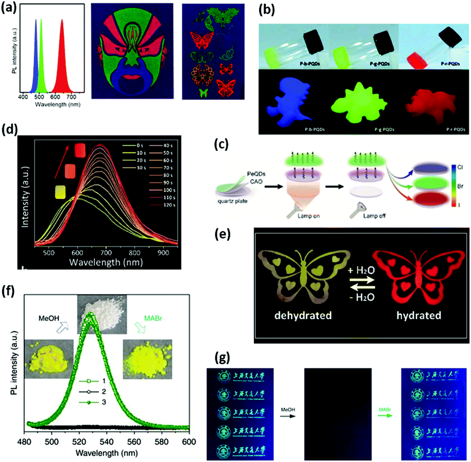 | ||
| Fig. 10 (a) PL spectra of red, green and blue colours on paper. Facial make-up full-colour image and full-colour fluorescent photo of sophisticated patterns. (b) 365 nm UV light photos of red, green and blue quantum dots, and colourful fluorescence cartoon sculptures made from red, green and blue quantum dots. (c) Illustration of full-spectrum persistent luminescence tuning. (d) Emission spectra recorded immediately after exposing the dehydrated (Cs2InBr5·H2O) to air. The three photographs show the colour changes of the dehydrated material under air upon photoexcitation. (e) Visualized dual emission between the hydrated and dehydrated (Cs2InBr5·H2O), fabricated by embedding the materials into an etched butterfly pattern. (f) Sequential optical images and PL emission spectra of MAPbBr3 NCs@Pb-MOF after one cycle of an impregnation-recovery process. 1, 2 and 3 represent the original, impregnated and recovered powder sample of MAPbBr3 NCs@Pb-MOF, respectively. (g) Reversible fluorescence switching of the MAPbBr3 NCs@Pb-MOF pattern in one encryption–decryption cycle (methanol impregnation for encryption and MABr spraying for decryption). Panels adapted from: a, reprinted with permission from ref. 439. Copyright (2019) American Chemical Society; b, reproduced from ref. 374 with permission from The Royal Society of Chemistry; c, reprinted with permission from ref. 440. Copyright (2019) John Wiley & Sons, Inc; d and e, reprinted with permission from ref. 221. Copyright (2019) John Wiley & Sons, Inc; f and g, ref. 441. | ||
5.1. Scintillators
ABX3-type halide perovskites have a long history as scintillator materials for radiation detection.103 Scintillation is the observable luminescence caused by the absorption of high-energy radiation or particles.442 Consequently, scintillators have been widely applied in a series of scientific and industrial fields, such as high-energy physics, medical imaging and geophysical exploration. Slow luminescent components constitute the main restrictive factor regarding the usage of scintillators, which relates to the intrinsic recombination luminescence from self-trapped excitons with a lifetime in the order of hundreds of microseconds. To fulfill the application requirements, the contribution of the delayed exciton luminescence should be minimized. A fast scintillation response speed comparable with BaF2 cross-luminescence has been achieved in Yb-rich YAlO3 single crystals.443 The direct band-gap semiconductor CsPbBr3 meets the requirements for radiation detection based on the evidence of its green PL emission when excited by a He–Cd laser, at 325 nm.1 Hybrid perovskite crystals, such as 3D MAPbI3, MAPbBr3 and 2D (EDBE)PbCl4, also exhibit X-ray scintillator characteristics, owing to the presence of heavy atoms.17 Compared to 3D perovskites, the thermal effects in 2D (EDBE)PbCl4 are significantly reduced due to the large exciton binding energy.5.2. LEDs, NIRs, LEDs, phosphors
The most remarkable application of luminescent perovskites lies in the fabrication of light emitting diodes (LEDs). The OIHPs have attracted much attention due to their tunable excitonic luminescence. In 1994, Era et al. fabricated an organic–inorganic heterostructure electroluminescent (EL) device using the combination of a layered perovskite compound ((C6H5C2H4NH3)2PbI4, PAPI) and an electron-transporting oxadiazole derivative.95 The EL device consisted of an indium–tin–oxid (ITO) anode, a PAPI emitter prepared by a spin-coating method from acetonitrile solution and an electron-transport layer of an oxadiazole derivative and an MgAg cathode. The heterostructure is displayed in Fig. 5(g) and (h). Driven at liquid-nitrogen temperature, an intense green emission peaking at 520 nm was observed, corresponding to the photoluminescent spectrum of the PAPI spin-coated film. However, the EL efficiency dropped dramatically due to the thermal luminescence quenching of the PAPI film, originating from the thermal ionization of the excitons. The light emitting devices typically employ two different morphologies of the layered perovskites: single crystals and spin-coated thin films. Single crystals are usually prepared from a solution phase rather than the melt phase, because the layered perovskites decompose before melting. Thin films can be easily spin-coated from solutions or by a vapour deposition process.444 In 2016, Wang et al. reported a multiple quantum wells LED with a very high external quantum efficiency of up to 11.7%.445 Kim et al. improved the luminescence efficiency of a formamidinium (FA, CH(NH2)2) lead bromide perovskite (FAPbBr3)-based LED by a ligand engineering method.446 Control of the ligand length has the effect of reducing the trap-assisted carrier recombination and improving charge injection and the transport capability in FAPbBr3 films. Lova et al. reported a potential industrial-scale production route for polymer-perovskite lighting devices by embedding the 2D perovskite (EDBE)PbCl4 in a flexible polymer, in which emission suppression and enhancement at specific wavelengths could be used to tune the emission colour over the entire visible spectrum without resorting to compositional engineering.447 Chin et al. continued to raise the external efficiency of green LEDs above 13% by coupling graded-size formamidinium lead bromide (FAPbBr3) NCs and microplatelets of octylammonium lead bromide perovskites.448 Single-component WL emitters were realized in the Cd-based 2D hybrid perovskite (C6H11NH3)2CdBr4. Upon 325 nm excitation, a broad-band WL emission was observed, consisting of an excitonic peak at 2.94 eV and a second peak at 2.53 eV resulting from the cyclohexylammonium cations emission.242The first use of completely inorganic CsPbBr3 thin films was achieved in 2015.18,19 Gangishetty et al. proposed an alternate transport layer structure in a perovskite LED to enable efficient emission across the entire blue–green spectral range.449 Khan et al. optimized a CsPbBr3-based LED device and achieved a significantly reduced turn-on voltage.450 Great advances have been achieved in improving the stability of all-inorganic perovskite quantum dots, such as by surface modification or encapsulation in polymer and glass. Shi et al. focused on the emission efficiency and operation stability of perovskite LEDs.189 CsPbBr3 quantum dot LEDs using n-ZnO and p-NiO carrier injectors can endure a high humidity (75%, 12 h) and a high working temperature (393 K) even without encapsulation. For highly flexible CsPbI3 perovskite LEDs fabricated by a photopolymer and ultrasmooth Ag films, good performance was maintained after 1000 times of repeated 180 degree stretch-release bending.451 Liu et al. presented a simple approach to improve the chemical stability by fabricating CsPbI3 quantum dots in zinc borosilicate glass through a conventional melting-quenching technique operated at 540 °C.452 CsPbBr3 NCs were embedded in a specially designed TeO2-based glass matrix, which showed a significant improvement in photon/thermal stability and water resistance.453 CsPbX3 (X = Br, I) NCs could be embedded into phosphosilicate glasses with low-melting (700 °C) temperature.454 The partial replacement of toxic Pb with Mn has also been reported in Mn-doped CsPb(Cl/Br)3 nanocrystal glass.455
Near-infrared (NIR) light-emitting diodes are used in a wide range of applications, including night vision, biomedical imaging, optical communications and computing. By embedding PbS quantum dots in a high-mobility hybrid perovskite matrix MAPbIxBr3−x, enhanced radiative recombination in the dots led to them exhibiting 1391 nm emission.456 A tunable near-infrared LED was fabricated based on lead-free organo-tin halide perovskite CH3NH3SnI3, achieving a 945 nm near-infrared emission.457 Increasing the bromide content led to shorter wavelength emissions, tunable down to 667 nm. Qiu et al. synthesized nanocrystalline methylammonium (MA) lead tin iodide films and used them to fabricate efficient NIR LEDs.458 The emission from the mixed lead–tin (Pb–Sn) halide perovskite was tunable from 850 to 950 nm, either by changing the Pb/Sn ratio or by incorporating bromide.
The deep red emission of Mn4+ (3d3) in the double perovskites La2LiSbO6 and La2MgTiO6 could be used to develop agricultural (horticultural) applications.338 Also under 342 nm excitation, NaLaMgWO6:Mn4+ and NaLaMgWO6:Mn4+ double-perovskite phosphors showed a high-efficiency far-red emission at approximately 700 nm, which suites the requirement for indoor plant growth.459
The other application of inorganic perovskite in LED fabrication is to serve as a phosphor in light downconversion and combination. For this, impurity doped phosphors have been widely investigated. Herein, great emphasis has been paid to inorganic halide perovskite nanocrystals. The CsPbBr3 QDs were chosen as red-emitting components to improve the colour rendering index (CRI) of Ce3+:YAG-based white LEDs.422 Owing to the narrow emission band, the colour gamut of CsPbX3 NCs could cover more than 140% of the NTSC (National Television System Committee) TV colour standard.460 CsPbBr3 QDs exhibited a narrow band with a FWHM at about 20 nm peaking at 534 nm461 However, the mass production of perovskite phosphors is critical for their wide application.462 Perovskite NCs synthesized by spray pyrolysis show an unprecedented stable absolute PLQY of ≈100% in both solution and in the solid-state neat film.463
5.3. Solar cells
Luminescent perovskites play an important role in solar cells. The efficiencies of inorganic–organic lead-halide perovskite solar cells have reached beyond 22% with photovoltages >1.2 V.464 Zhou et al. fabricated a novel type of quantum cutting material, CsPbCl1.5Br1.5:Yb3+,Ce3+ NCs, which could realize the emission of multiple near-infrared photons for each ultraviolet/visible photon absorbed, which improved the photoelectric conversion efficiency (PCE) of solar cells.283 Pazos-Outon et al. showed that methyl ammonium lead iodide (MAPbI3) likewise has a larger Auger coefficient that expected.465 An efficient YCl3-treated TiO2 electron-transfer layer was used to fabricate perovskite solar cells with enhanced photovoltaic performance and less hysteresis.466 The improved perovskite/TiO2 interface with YCl3 treatment was found to separate and extract photogenerated charge rapidly and to effectively suppress recombination. Li et al. provided a facile approach to fabricate core–shell perovskite solar cells with high efficiency and long-term stability against moisture.467 The authors introduced gallium(III) acetylacetonate (GaAA3) as a precursor additive to in situ induce a metal–organic-complex monomolecular intermediate ([GaAA3]4), which allowed realizing CsxFA1−xPbI3–[GaAA3]4 (0 < x < 1) hybrid perovskite materials. The formed hybrid perovskites were proven to possess a CsxFA1−xPbI3 core and [GaAA3]4 shell. It was reported that surface passivation can be combined with optimized charge carrier selective interfaces to increase the power conversion efficiency of hybrid perovskite (MAPbI3) thin film solar cells.468 Rajagopal et al. incorporated phenylethylammonium (PEA) in a mixed-halide perovskite composition MAPb(I0.6Br0.4)3 to solve the inherent material-level challenges in 1.80–1.85 eV Eg perovskites.469 The power conversion efficiency of the lead-free Cs3Bi2I9 mesoscopic solar cells was limited by the poor photocurrent density. Therefore, a continuous network of a 3D crystal structure is more favourable.4705.4. Lasers, non-linear optics, indicators
Deschler et al. constructed and demonstrated the operation of an optically pumped vertical cavity laser comprising a layer of perovskite between a dielectric mirror and evaporated gold top mirrors.471 The observed broad homogeneous line width in MAPbI3−xClx ought to allow amplification of Fourier-transform-limited pulses with sub-100 fs duration, making these materials interesting for pulsed laser operation.472 The optical-pumped rectangular cross-sectional perovskite MAPbI3 nanowire lasers had a near-infrared wavelength of 777 nm, low threshold of 11 μJ cm−2 and a quality factor as high as 405.473 Liu et al. systematically investigated the temperature-dependent spontaneous emission and lasing spectra of chemical vapour deposited CsPbBr3.474Two-photon absorption-induced luminescence is a typical third-order nonlinear optical process. It has been investigated in perovskite CsPbBr3 quantum dots at a broad temperature range.475 The PL spectrum excited by two-photon absorption exhibits different temperature-dependent spectral shift behaviour than general semiconductors, and is probably caused by thermal expansion, electron–phonon interaction and structural phase transition. The inefficient photoluminescence was enhanced by constructing a hybrid dielectric structure, in which a 2D perovskite flake phenylethylamine lead iodide ((PEA)2PbI4) was covered by dielectric microspheres (approximately micrometers in diameter).476 The emission increased by two orders of magnitude in the hybrid dielectric structure due to the cooperative enhancement of the detection efficiency and quantum efficiency of the 2D perovskite.
Blue-light emission at room temperature from Ar+-irradiated SrTiO3 single crystals could be applied in displays and indicators.477 Besides Ar+-irradiated oxygen-deficient SrTiO3, substituting La3+ for Sr2+ and Nb5+ for Ti4+ in SrTiO3 provided electron carriers in Ti 3d conduction bands, which were responsible for the room-temperature blue-light emission.478 The emitting region can be patterned into any size and shape with conventional microscopic fabrication techniques.
5.5. Temperature sensors
BaTiO3 doped by lanthanide ions (0.3 mol% Er3+/3.0 mol% Yb3+) can be used as a temperature sensor with a maximum sensitivity of 0.00475 K−1 at 430 K.438 MgTiO3 nanoparticles doped with Mn4+ were also synthesized as optical thermal sensors to take advantage of the drastic variations of Mn4+ luminescence with temperatures.479 The temperature evolution of the infrared luminescence of yttrium orthoaluminate nano-perovskite, YAlO3, doped with 1.0 mol% of Nd3+ ions, could be used for both sub-tissue luminescence imaging and luminescence-based thermal sensing.480 The Mn4+-doped Y2MgTiO6 phosphors showed far-red emission at ∼715 nm, with a maximum sensor sensitivity as high as 0.00142 K−1 at 153 K.481 The thermochromism of organic/inorganic halide perovskites Cs4PbBr6 has been studied for potential applications as photoluminescence-based temperature sensors.482 Pr3+-Doped triple-layered perovskite Na2La2Ti3O10 microcrystals promise remarkable performance for temperature sensing over a wide temperature range (125–533 K), with a maximum relative sensitivity of 2.43% K−1 at 423 K.4835.6. Upconversion, persistent luminescence
Upconversion luminescence could be used to detect IR or NIR light. Usually, nonlinear upconversion luminescence is limited by a small cross-section of multiphoton absorption. Methylammonium lead halide perovskites were combined with erbium silicate nanosheets to give a remarkable spectral response at 1.54 μm. Strong upconversion luminescence from the nanosheets was well confined in cavities, which simultaneously excited the neighbouring perovskite to realize photodetection.484 Considering the large absorption coefficient and high PLQY, a convenient approach to realize upconversion luminescence in perovskite quantum dots was reported by Zheng et al. through a sensitization by lanthanide-doped nanoparticles.187 The sensitization was governed by a radiative energy-transfer upconversion process, and according to Zeng et al., the energy-transfer efficiency between upconversion nanoparticle donors and quantum dot acceptors approached nearly 100%.485 Under NIR laser light irradiation, intense green emission from the perovskite CsPbBr3 quantum dots through BaYF5:Yb,Ln sensitization was observed even in a liquid suspension. Ma et al. reported WL emission from composites of high-quality CsPbBr3 quantum dots and β-NaYF4:30%Yb,0.2%Tm nanoparticles triggered by 980 nm NIR excitation.486 The luminescence of the quantum dots was excited by the upconversion luminescence of the nanoparticles. WL emission was achieved from the composite sample with regulation of the concentration. The upconversion luminescence of perovskite quantum dots has received less attention due to the lack of anti-Stokes luminescence properties of the material itself. However, Duan et al. observed upconversion luminescence in CsPb(Br/I)3 NCs under laser excitation with a wavelength of 635–700 nm. The emission peaks located at 632 nm were consistent with the normal PL emission of CsPb(Br/I)3 NCs excited by 400 nm UV light.487 Therefore, more research is needed to unravel the upconversion luminescent properties in perovskite quantum dots.Persistent luminescent materials are applied as night or dark-light vision indicators. All-inorganic CsPbX3 (X = Cl, Br and I) perovskite quantum dots could be combined with the traditional afterglow phosphor CaAl2O4:1%Eu2+,0.5%Nd3+ to produce tunable persistent luminescence covering the full spectrum. The perovskite quantum dots work as light-convertors to absorb the persistently released violet and blue afterglow light and then produce emissions tunable over the entire visible spectral region. In addition, the afterglow decays of different spectral components are highly synchronized due to the same light source.440 The other strategy for persistent luminescence depends on the direct energy transfer from hybrid perovskites into the triplet states of organic molecules. Hu et al. reported a 0.2 ms afterglow duration in the 2D perovskite (TTMA)2PbBr4(TPB) by performing molecular engineering of the OIHPs. The excitonic emission peak of TPB was located at 420 nm under 390 nm excitation, whereas a weak emission peak at 590 nm corresponded to the phosphorescence from the organic cation TTMABr molecule. Nonradiative recombination was suppressed by the mixed-cation perovskites with a phosphorescence yield of 11.2%. The persistent luminescence colour could be tuned by incorporating different organic cations into the hybrid perovskites. Following this strategy, novel persistent luminescence could be explored in other 2D perovskite systems by changing the dimensionality and the chemical composition.488
5.7. Information encryption and decryption
Luminescent perovskites have “smart” functions when applied in confidential information encryption and decryption. In cesium lead halide nanostructures, quantum-confined few-monolayer nanoplatelets are converted to the bulk phase under very low irradiation intensity (≈20 mW cm−2).489 Benefiting from the remarkable emission colour change during photon-driven transformation, multicolour luminescence photopatterns and facile information photo-encoding can be established. Zhang et al. realized confidential information protection and storage by converting lead-based metal–organic frameworks into luminescent perovskite NCs. By polar solvents impregnation and halide salt conversion, the quenching and recovery of the luminescence lead to reversible on/off switching of the luminescence signal for multiple information encryption and decryption processes.441 In perovskite NCs CsPbX3 (X = Cl, Br, and I), the molecular chirality can transfer to the NCs, resulting in circularly polarized luminescence signals.490 In addition, confidential information protection can be realized through the anion-exchange reaction of perovskite quantum dots, and emission colour-encoding patterns could be designed by an inkjet-printing technique. The conversion of luminescent 3D from a colourless 0D perovskite is achieved by reaction with invisible halide salts. Therefore, the reversible off/on switching of the luminescence can be used to encrypt and decrypt confidential information.439 Fan et al. fabricated methyl ammonium lead tri-bromide perovskite metasurfaces. Here, the encoded information was visible only when the incident laser was on-resonance, as off-resonance pumping and single-photon excitation just produced a uniform dark background.491The use of perovskite NCs as inks was reported by Akkerman et al.492 Pure Cs4PbX6 (X = Cl, Br, I) and mixed halide compositional NCs with sizes ranging from 9 to 37 nm were synthesized by a colloidal method. They had no visible excitonic emission due to their large band gap. The absorption bands belonging to samples with mixed halide composition were located in the intermediate spectral position between those of the pure halide compounds. Pan et al. synthesized extremely stable CsPbX3 nanocrystal–polymer composites as solution-processable luminescent inks with remarkable chemical stability towards water.493
5.8. Photosensors
Perovskite materials can be used for photodetection due to their high external quantum efficiency and rapid temporal response. Zheng et al. fabricated a 2D photodetector from high-crystallinity 2D CsPbBr3 perovskites micro-/nanoflakes494 Duan synthesized MAPbBr3 microdisk arrays with a uniform size distribution and emission spectra and fabricated a perovskite photodetector array with fast rise (<8.3 ms) and decay (<8.3 ms) times.487Room-temperature red luminescence was observed in a 2D layered hybrid lead halide [CH(NH2)2][C(NH2)3]PbI4, together with photoconductivity.495 The co-existance of the excitonic emission and photoconductivity in hybrid perovskites is rather rare due to the competion between the two processes, as reflected by the low quantum yield of 3.5%. The photoconductivity has a dark specific resistivity value of 1 × 10¹⁰ Ω cm, indicating a rather low intrinsic carrier concentration and/or mobility. However, whether trap states or self-trapped excitons cause this photoconductivity remains unclear.
5.9. Stress sensors
Luminescent perovskites could be fabricated into sensors to detect stress or pressure. Sr3Sn2O7:Sm3+ has strong reddish–orange emission under compressive load, which is visible to the naked eye.114 Ma et al. observed pressure-induced emission in initially nonfluorescent 0D perovskite quantum dots Cs4PbBr6 under a high pressure of 3.01 GPa.496 The emission intensified under further compression. This luminescence stems from the enhanced optical activity and the increased binding energy of self-trapped excitons. This phenomenon is ascribed to the large distortion of [PbBr6]4− octahedral motifs resulting from a structural phase transition.5.10. Ferroelectricity and photochemical reactions
Zhang et al. constructed 3D organic–inorganic perovskite ferroelectrics by the symmetry reduction of spherical moieties497 Halide perovskite quantum dots could be used in photochemical conversion (e.g. water splitting or CO2 reduction). Xu et al. constructed CsPbBr3 quantum dot/graphene oxide composite for photocatalytic CO2 reduction. Introduction of the conductive graphene oxide caused a photocatalytic enhancement.4986. Conclusion and outlook
Perovskite materials are arousing great research interests due to their excellent luminescence performance. Perovskites have the general formula of ABO3 and occur both naturally (e.g. CaTiO3) and synthetically, and can form a wide-range class of derivatives. According to their crystal structure, they can be divided into three sub-classes: standard perovskites, low-D perovskites and perovskite-like halides. We rationalized the luminescence behaviours and various crystal structure types in oxide perovskites and halide perovskites to probe for a potential relationship between the crystal structure, electronic structure and luminescent properties. Perovskite nanomaterials have shown high light emission efficiency with a decrease in their physical dimensionality or crystal structure dimensionality. The electronic migration is more restricted in these cases, leading to a larger exciton binding energy and higher PLQY. Based on the high PLQY of perovskite materials, their use in fabricating illuminating device opens a broad application field. Various material stability and PL efficiency improving methods have been developed by researchers, including surface passivation, encapsulation and doping, to pave the way for practical applications. This review summarized previous research on the structural design, optical property characterizations and property improvements of perovskite-related compounds, but there are still a lot of future research opportunities in this field. At present, the intentional design of high PLQY materials is still challenging, and more efforts are needed to further clarify the relationship between the crystal structure, electronic structure and luminescence properties in the future.Based on the above, the future development of luminescent perovskites can be focused on the following challenges: 1. gaining a deep understanding of the luminescent properties. For transition-metal and rare-earth elements-doped oxide perovskites, it is important to establish the relationship between the energy level structure and chemical composition/crystal structure by analyzing the crystal-field and nephelauxetic effects. For organic–inorganic hybrid and all-inorganic perovskite nanocrystals, some basic luminescent mechanisms need clarification. For example, there are conflicting reports on the luminescence of CsPbBr3/Cs4PbBr6, and reports where the relative ordering of dark and bright exciton sublevels in the halide perovskites CsPbX3 and FAPbBr3 is just the opposite. 2. Improving the surface stability and luminescent efficiency by doping engineering. This is promising to explore the effects of transition-metal and rare-earth elements on surface passivation, and on the defects repair and surface healing of organic–inorganic hybrid and all-inorganic perovskite nanocrystals. 3. The discovery of new Pb-free all-inorganic perovskite nanocrystals. Materials that are less toxic while retaining their luminescence will gain much practical applications in the future.
Conflicts of interest
There are no conflicts to declare.Acknowledgements
This work is supported by the National Natural Science Foundation of China (No. 51832005, 51602019 and 51702329), Beijing Natural Science Foundation (2182080) and Fundamental Research Funds for the Central Universities (FRF-TP-18-005A1 and FRF-TP-18-002C1).Notes and references
- C. C. Stoumpos, C. D. Malliakas, J. A. Peters, Z. Liu, M. Sebastian, J. Im, T. C. Chasapis, A. C. Wibowo, D. Y. Chung, A. J. Freeman, B. W. Wessels and M. G. Kanatzidis, Cryst. Growth Des., 2013, 13, 2722–2727 CrossRef CAS.
- S. A. Veldhuis, P. P. Boix, N. Yantara, M. Li, T. C. Sum, N. Mathews and S. G. Mhaisalkar, Adv. Mater., 2016, 28, 6804–6834 CrossRef CAS PubMed.
- Z. Cheng and J. Lin, CrystEngComm, 2010, 12, 2646 RSC.
- P. F. Smet, I. Moreels, Z. Hens and D. Poelman, Materials, 2010, 3, 2834–2883 CrossRef CAS.
- X. Liu, D. Yu, X. Song and H. Zeng, Small, 2018, 14, e1801460 CrossRef PubMed.
- H. L. Wells, Z. Anorg. Chem., 1893, 3, 195–210 CrossRef.
- C. K. Møller, Nature, 1958, 182, 1436 CrossRef.
- D. E. Scaife, P. F. Weller and W. G. Fisher, J. Solid State Chem., 1974, 9, 308–314 CrossRef CAS.
- D. Weber, Z. Naturforsch., B: J. Chem. Sci., 1978, 33, 1443–1445 Search PubMed.
- A. Kojima, K. Teshima, Y. Shirai and T. Miyasaka, J. Am. Chem. Soc., 2009, 131, 6050–6051 CrossRef CAS PubMed.
- W. S. Yang, B.-W. Park, E. H. Jung, N. J. Jeon, Y. C. Kim, D. U. Lee, S. S. Shin, J. Seo, E. K. Kim, J. H. Noh and S. I. Seok, Science, 2017, 356, 1376–1379 CrossRef CAS PubMed.
- D. B. Mitzi, S. Wang, C. A. Feild, C. A. Chess and A. M. Guloy, Science, 1995, 267, 1473–1476 CrossRef CAS PubMed.
- M. Wiegel, M. Hamoumi and G. Blasse, Mater. Chem. Phys., 1994, 36, 289–293 CrossRef CAS.
- W. Tress, N. Marinova, O. Inganas, M. K. Nazeeruddin, S. M. Zakeeruddin and M. Graetzel, Adv. Energy Mater., 2015, 5, 1400812 CrossRef.
- C. M. Sutter-Fella, Y. Li, M. Amani, J. W. Ager, F. M. Toma, E. Yablonovitch, I. D. Sharp and A. Javey, Nano Lett., 2016, 16, 800–806 CrossRef CAS PubMed.
- L. M. Pazos-Outon, M. Szumilo, R. Lamboll, J. M. Richter, M. Crespo-Quesada, M. Abdi-Jalebi, H. J. Beeson, M. Vrucinic, M. Alsari, H. J. Snaith, B. Ehrler, R. H. Friend and F. Deschler, Science, 2016, 351, 1430–1433 CrossRef CAS PubMed.
- M. D. Birowosuto, D. Cortecchia, W. Drozdowski, K. Brylew, W. Lachmanski, A. Bruno and C. Soci, Sci. Rep., 2016, 6, 37254 CrossRef CAS PubMed.
- N. Yantara, S. Bhaumik, F. Yan, D. Sabba, H. A. Dewi, N. Mathews, P. P. Boix, H. V. Demir and S. Mhaisalkar, J. Phys. Chem. Lett., 2015, 6, 4360–4364 CrossRef CAS PubMed.
- Y. Kim, E. Yassitepe, O. Voznyy, R. Comin, G. Walters, X. Gong, P. Kanjanaboos, A. F. Nogueira and E. H. Sargent, ACS Appl. Mater. Interfaces, 2015, 7, 25007–25013 CrossRef CAS PubMed.
- A. Kudo, H. Kato and S. Nakagawa, J. Phys. Chem. B, 2000, 104, 571–575 CrossRef CAS.
- M. Machida, J. Yabunaka and T. Kijima, Chem. Mater., 2000, 12, 812–817 CrossRef CAS.
- K. Maeda, M. Eguchi and T. Oshima, Angew. Chem., Int. Ed., 2014, 53, 13164–13168 CrossRef CAS PubMed.
- L. Johnson, H. Guggenheim and R. Thomas, Phys. Rev., 1966, 149, 179 CrossRef CAS.
- K. Gauthron, J.-S. Lauret, L. Doyennette, G. Lanty, A. Al Choueiry, S. J. Zhang, A. Brehier, L. Largeau, O. Mauguin, J. Bloch and E. Deleporte, Opt. Express, 2010, 18, 5912 CrossRef CAS PubMed.
- T. Kondo, T. Azuma, T. Yuasa and R. Ito, Solid State Commun., 1998, 105, 253–255 CrossRef CAS.
- M. Johnsson and P. Lemmens, in Handbook of Magnetism and Advanced Magnetic Materials, American Cancer Society, 2007 Search PubMed.
- D. B. Mitzi, in Progress in Inorganic Chemistry, John Wiley & Sons, Ltd, 2007, pp. 1–121 Search PubMed.
- X. Li, F. Cao, D. Yu, J. Chen, Z. Sun, Y. Shen, Y. Zhu, L. Wang, Y. Wei, Y. Wu and H. Zeng, Small, 2017, 13, 1603996 CrossRef PubMed.
- Y. Zhang, W. Jie, P. Chen, W. Liu and J. Hao, Adv. Mater., 2018, 30, 1707007 CrossRef PubMed.
- D. Chen and X. Chen, J. Mater. Chem. C, 2019, 7, 1413–1446 RSC.
- D. Cortecchia, J. Yin, A. Petrozza and C. Soci, J. Mater. Chem. C, 2019, 7, 4956–4969 RSC.
- D. B. Mitzi, J. Chem. Soc., Dalton Trans., 2001, 1–12 RSC.
- S. Zhang, G. Lanty, J.-S. Lauret, E. Deleporte, P. Audebert and L. Galmiche, Acta Mater., 2009, 57, 3301–3309 CrossRef CAS.
- F. S. Galasso, Structure, properties and preparation of perovskite-type compounds: international series of monographs in solid state physics, Elsevier, 2013, vol. 5 Search PubMed.
- J. Breternitz and S. Schorr, Adv. Energy Mater., 2018, 8, 1802366 CrossRef.
- A. Jodlowski, D. Rodríguez-Padrón, R. Luque and G. de Miguel, Adv. Energy Mater., 2018, 8, 1703120 CrossRef.
- L. Mao, P. Guo, M. Kepenekian, I. Hadar, C. Katan, J. Even, R. D. Schaller, C. C. Stoumpos and M. G. Kanatzidis, J. Am. Chem. Soc., 2018, 140, 13078–13088 CrossRef CAS PubMed.
- Z. Cheng and J. Lin, CrystEngComm, 2010, 12, 2646 RSC.
- M. A. Peña and J. L. G. Fierro, Chem. Rev., 2001, 101, 1981–2018 CrossRef.
- E. Salje, Acta Crystallogr., Sect. B: Struct. Crystallogr. Cryst. Chem., 1977, 33, 574–577 CrossRef.
- O. Knop, R. E. Wasylishen, M. A. White, T. S. Cameron and M. J. M. V. Oort, Can. J. Chem., 1990, 68, 412–422 CrossRef CAS.
- Y. Doi and Y. Hinatsu, J. Phys.: Condens. Matter, 1999, 11, 4813–4820 CrossRef CAS.
- F. Giustino and H. J. Snaith, ACS Energy Lett., 2016, 1, 1233–1240 CrossRef CAS.
- X. G. Zhao, D. Yang, Y. Sun, T. Li, L. Zhang, L. Yu and A. Zunger, J. Am. Chem. Soc., 2017, 139, 6718–6725 CrossRef CAS.
- E. Meyer, D. Mutukwa, N. Zingwe and R. Taziwa, Metals, 2018, 8, 667 CrossRef.
- S. F. Hoefler, G. Trimmel and T. Rath, Monatsh. Chem., 2017, 148, 795–826 CrossRef CAS PubMed.
- J. H. Lee, G. Luo, I. C. Tung, S. H. Chang, Z. Luo, M. Malshe, M. Gadre, A. Bhattacharya, S. M. Nakhmanson, J. A. Eastman, H. Hong, J. Jellinek, D. Morgan, D. D. Fong and J. W. Freeland, Nat. Mater., 2014, 13, 879–883 CrossRef CAS PubMed.
- B. Chabot and E. Parthe, Acta Crystallogr., Sect. B: Struct. Crystallogr. Cryst. Chem., 1978, 34, 645–648 CrossRef.
- A. J. Lehner, D. H. Fabini, H. A. Evans, C.-A. Hébert, S. R. Smock, J. Hu, H. Wang, J. W. Zwanziger, M. L. Chabinyc and R. Seshadri, Chem. Mater., 2015, 27, 7137–7148 CrossRef CAS.
- A. E. Maughan, A. M. Ganose, M. M. Bordelon, E. M. Miller, D. O. Scanlon and J. R. Neilson, J. Am. Chem. Soc., 2016, 138, 8453–8464 CrossRef CAS PubMed.
- N. Sakai, A. A. Haghighirad, M. R. Filip, P. K. Nayak, S. Nayak, A. Ramadan, Z. Wang, F. Giustino and H. J. Snaith, J. Am. Chem. Soc., 2017, 139, 6030–6033 CrossRef CAS PubMed.
- H. A. Evans, D. H. Fabini, J. L. Andrews, M. Koerner, M. B. Preefer, G. Wu, F. Wudl, A. K. Cheetham and R. Seshadri, Inorg. Chem., 2018, 57, 10375–10382 CrossRef CAS PubMed.
- T. Ishihara, J. Lumin., 1994, 60–61, 269–274 CrossRef CAS.
- P. Day, R. J. Gillespie and P. Day, Philos. Trans. R. Soc., A, 1985, 314, 145–158 CrossRef.
- H. Arend, W. Huber, F. H. Mischgofsky and G. K. Richter-Van Leeuwen, J. Cryst. Growth, 1978, 43, 213–223 CrossRef CAS.
- T. Ishihara, J. Takahashi and T. Goto, Phys. Rev. B: Condens. Matter Mater. Phys., 1990, 42, 11099–11107 CrossRef CAS PubMed.
- D. B. Mitzi, Inorg. Chem., 2000, 39, 6107–6113 CrossRef CAS PubMed.
- L. Mao, C. C. Stoumpos and M. G. Kanatzidis, J. Am. Chem. Soc., 2019, 141, 1171–1190 CrossRef CAS PubMed.
- J. Guan, Z. Tang and A. M. Guloy, Chem. Commun., 1999, 1833–1834 RSC.
- Y. Y. Li, C. K. Lin, G. L. Zheng, Z. Y. Cheng, H. You, W. D. Wang and J. Lin, Chem. Mater., 2006, 18, 3463–3469 CrossRef CAS.
- Y. Li, G. Zheng and J. Lin, Eur. J. Inorg. Chem., 2008, 2008, 1689–1692 CrossRef.
- L. Mao, H. Tsai, W. Nie, L. Ma, J. Im, C. C. Stoumpos, C. D. Malliakas, F. Hao, M. R. Wasielewski, A. D. Mohite and M. G. Kanatzidis, Chem. Mater., 2016, 28, 7781–7792 CrossRef CAS.
- L. Mao, Y. Wu, C. C. Stoumpos, M. R. Wasielewski and M. G. Kanatzidis, J. Am. Chem. Soc., 2017, 139, 5210–5215 CrossRef CAS PubMed.
- X. Li, P. Guo, M. Kepenekian, I. Hadar, C. Katan, J. Even, C. C. Stoumpos, R. D. Schaller and M. G. Kanatzidis, Chem. Mater., 2019, 31, 3582–3590 CrossRef CAS.
- C. C. Stoumpos, D. H. Cao, D. J. Clark, J. Young, J. M. Rondinelli, J. I. Jang, J. T. Hupp and M. G. Kanatzidis, Chem. Mater., 2016, 28, 2852–2867 CrossRef CAS.
- C. M. M. Soe, G. P. Nagabhushana, R. Shivaramaiah, H. Tsai, W. Nie, J. C. Blancon, F. Melkonyan, D. H. Cao, B. Traore, L. Pedesseau, M. Kepenekian, C. Katan, J. Even, T. J. Marks, A. Navrotsky, A. D. Mohite, C. C. Stoumpos and M. G. Kanatzidis, Proc. Natl. Acad. Sci. U. S. A., 2018, 116, 58–66 CrossRef PubMed.
- J. Calabrese, N. L. Jones, R. L. Harlow, N. Herron, D. L. Thorn and Y. Wang, J. Am. Chem. Soc., 1991, 113, 2328–2330 CrossRef CAS.
- D. H. Cao, C. C. Stoumpos, O. K. Farha, J. T. Hupp and M. G. Kanatzidis, J. Am. Chem. Soc., 2015, 137, 7843–7850 CrossRef CAS PubMed.
- B. M. Benin, D. N. Dirin, V. Morad, M. Woerle, S. Yakunin, G. Raino, O. Nazarenko, M. Fischer, I. Infante and M. V. Kovalenko, Angew. Chem., Int. Ed., 2018, 57, 11329–11333 CrossRef CAS PubMed.
- F. Zhu, L. Men, Y. Guo, Q. Zhu, U. Bhattacharjee, P. M. Goodwin, J. W. Petrich, E. A. Smith and J. Vela, ACS Nano, 2015, 9, 2948–2959 CrossRef CAS PubMed.
- S. Huang, Z. Li, B. Wang, N. Zhu, C. Zhang, L. Kong, Q. Zhang, A. Shan and L. Li, ACS Appl. Mater. Interfaces, 2017, 9, 7249–7258 CrossRef CAS PubMed.
- H. Diab, G. Trippe-Allard, F. Ledee, K. Jemli, C. Vilar, G. Bouchez, V. L. R. Jacques, A. Tejeda, J. Even, J.-S. Lauret, E. Deleporte and D. Garrot, J. Phys. Chem. Lett., 2016, 7, 5093–5100 CrossRef CAS PubMed.
- T. C. Jellicoe, J. M. Richter, H. F. J. Glass, M. Tabachnyk, R. Brady, S. E. Dutton, A. Rao, R. H. Friend, D. Credgington, N. C. Greenham and M. L. Boehm, J. Am. Chem. Soc., 2016, 138, 2941–2944 CrossRef CAS PubMed.
- S. Ghosh and B. Pradhan, ChemNanoMat, 2019, 5, 300–312 CrossRef CAS.
- G. Li, H. Wang, T. Zhang, L. Mi, Y. Zhang, Z. Zhang, W. Zhang and Y. Jiang, Adv. Funct. Mater., 2016, 26, 8478–8486 CrossRef CAS.
- D. N. Dirin, L. Protesescu, D. Trummer, I. V. Kochetygov, S. Yakunin, F. Krumeich, N. P. Stadie and M. V. Kovalenko, Nano Lett., 2016, 16, 5866–5874 CrossRef CAS PubMed.
- D. Chen, J. Li, X. Chen, J. Chen and J. Zhong, ACS Appl. Mater. Interfaces, 2019, 11, 10059–10067 CrossRef CAS PubMed.
- I. Borriello, G. Cantele and D. Ninno, Phys. Rev. B: Condens. Matter Mater. Phys., 2008, 77, 235214 CrossRef.
- A. Filippetti and A. Mattoni, Phys. Rev. B: Condens. Matter Mater. Phys., 2014, 89, 125203 CrossRef.
- I. Borriello, G. Cantele and D. Ninno, Phys. Rev. B: Condens. Matter Mater. Phys., 2008, 77, 235214 CrossRef.
- P. A. Rodnyi, Radiat. Meas., 2004, 38, 343–352 CrossRef CAS.
- M. A. Becker, R. Vaxenburg, G. Nedelcu, P. C. Sercel, A. Shabaev, M. J. Mehl, J. G. Michopoulos, S. G. Lambrakos, N. Bernstein, J. L. Lyons, T. Stoferle, R. F. Mahrt, M. V. Kovalenko, D. J. Norris, G. Raino and A. L. Efros, Nature, 2018, 553, 189–193 CrossRef CAS PubMed.
- P. Tamarat, M. I. Bodnarchuk, J.-B. Trebbia, R. Erni, M. V. Kovalenko, J. Even and B. Lounis, Nat. Mater., 2019, 18, 717–724 CrossRef CAS PubMed.
- L. I. Van Steensel, S. G. Bokhove, A. M. Van de Craats, J. De Blank and G. Blasse, Mater. Res. Bull., 1995, 30, 1359–1362 CrossRef CAS.
- J. T. W. de Hair and G. Blasse, J. Lumin., 1973, 8, 97–100 CrossRef CAS.
- H. Witzmann, H. Anderson and D. Walther, Z. Phys. Chem., 1968, 239, 243 CAS.
- S. Lizzo, A. Meijerink, G. J. Dirksen and G. Blasse, Chem. Phys. Lett., 1996, 253, 108–112 CrossRef CAS.
- A. Braam and G. Blasse, Solid State Commun., 1976, 20, 717–719 CrossRef CAS.
- J. L. Sommerdijk and A. Bril, J. Lumin., 1976, 11, 363–367 CrossRef CAS.
- S. Baccaro, K. Blaẑek, F. de Notaristefani, P. Maly, J. A. Mares, R. Pani, R. Pellegrini and A. Soluri, Nucl. Instrum. Methods Phys. Res., Sect. A, 1995, 361, 209–215 CrossRef CAS.
- A. Lempicki, M. H. Randles, D. Wisniewski, M. Balcerzyk, C. Brecher and A. J. Wojtowicz, IEEE Trans. Nucl. Sci., 1995, 42, 280–284 CrossRef CAS.
- B. Bouma and G. Blasse, J. Phys. Chem. Solids, 1995, 56, 261–265 CrossRef CAS.
- G. C. Papavassiliou and I. B. Koutselas, Synth. Met., 1995, 71, 1713–1714 CrossRef CAS.
- A. M. Srivastava, J. F. Ackerman and W. W. Beers, J. Solid State Chem., 1997, 134, 187–191 CrossRef CAS.
- M. Era, S. Morimoto, T. Tsutsui and S. Saito, Appl. Phys. Lett., 1994, 65, 676–678 CrossRef CAS.
- M. Wiegel, M. Emond, E. Stobbe and G. Blasse, J. Phys. Chem. Solids, 1994, 55, 773–778 CrossRef CAS.
- T. Hattori, T. Taira, M. Era, T. Tsutsui and S. Saito, Chem. Phys. Lett., 1996, 254, 103–108 CrossRef CAS.
- E. Danielson, M. Devenney, D. M. Giaquinta, J. H. Golden, R. C. Haushalter, E. W. McFarland, D. M. Poojary, C. M. Reaves, W. H. Weinberg and X. D. Wu, Science, 1998, 279, 837–839 CrossRef CAS PubMed.
- D. B. Mitzi, M. T. Prikas and K. Chondroudis, Chem. Mater., 1999, 11, 542–544 CrossRef CAS.
- A. Kudo, Chem. Mater., 1997, 9, 664–669 CrossRef CAS.
- A. Kudo and T. Sakata, J. Phys. Chem., 1995, 99, 15963–15967 CrossRef CAS.
- A. M. Srivastava and W. W. Beers, J. Electrochem. Soc., 1996, 143, L203–L205 CrossRef CAS.
- A. V. Gektin, J. Lumin., 2000, 87–89, 1283–1285 CrossRef CAS.
- J. T. W. De Hair and G. Blasse, J. Solid State Chem., 1976, 19, 263–270 CrossRef CAS.
- M. Nikl, K. Nitsch, K. Polak, G. P. Pazzi, P. Fabeni, D. S. Citrin and M. Gurioli, Phys. Rev. B: Condens. Matter Mater. Phys., 1995, 51, 5192–5199 CrossRef CAS PubMed.
- K. Tanaka, T. Takahashi, T. Kondo, K. Umeda, K. Ema, T. Umebayashi, K. Asai, K. Uchida and N. Miura, Jpn. J. Appl. Phys., 2005, 44, 5923–5932 CrossRef CAS.
- D. B. Mitzi and K. Liang, Chem. Mater., 1997, 9, 2990–2995 CrossRef CAS.
- J. Li, C.-N. Xu, D. Tu, X. Chai, X. Wang, L. Liu and E. Kawasaki, Acta Mater., 2018, 145, 462–469 CrossRef CAS.
- M. L. Moreira, E. C. Paris, G. S. do Nascimento, V. M. Longo, J. R. Sambrano, V. R. Mastelaro, M. I. B. Bernardi, J. Andrés, J. A. Varela and E. Longo, Acta Mater., 2009, 57, 5174–5185 CrossRef CAS.
- H. Mizoguchi, H. W. Eng and P. M. Woodward, Inorg. Chem., 2004, 43, 1667–1680 CrossRef CAS PubMed.
- H. Kato, H. Kobayashi and A. Kudo, J. Phys. Chem. B, 2002, 106, 12441–12447 CrossRef CAS.
- X. Lao, X. Li, H. Agren and G. Chen, Nanomaterials, 2019, 9, 172 CrossRef CAS PubMed.
- S. Niu, H. Huyan, Y. Liu, M. Yeung, K. Ye, L. Blankemeier, T. Orvis, D. Sarkar, D. J. Singh, R. Kapadia and J. Ravichandran, Adv. Mater., 2017, 29, 1604733 CrossRef PubMed.
- S. Kamimura, H. Yamada and C.-N. Xu, Appl. Phys. Lett., 2012, 101, 091113 CrossRef.
- G. Zhou, X. Jiang, J. Zhao, M. Molokeev, Z. Lin, Q. Liu and Z. Xia, ACS Appl. Mater. Interfaces, 2018, 10, 24648–24655 CrossRef CAS PubMed.
- J. Zhong, D. Chen, S. Yuan, M. Liu, Y. Yuan, Y. Zhu, X. Li and Z. Ji, Inorg. Chem., 2018, 57, 8978–8987 CrossRef CAS.
- H. Wu, Y. Yang, D. Zhou, K. Li, J. Yu, J. Han, Z. Li, Z. Long, J. Ma and J. Qiu, Nanoscale, 2018, 10, 3429–3437 RSC.
- B. Kang and K. Biswas, J. Phys. Chem. Lett., 2018, 9, 830–836 CrossRef CAS PubMed.
- X. Hong, T. Ishihara and A. V. Nurmikko, Phys. Rev. B: Condens. Matter Mater. Phys., 1992, 45, 6961–6964 CrossRef CAS PubMed.
- P. Tyagi, S. M. Arveson and W. A. Tisdale, J. Phys. Chem. Lett., 2015, 6, 1911–1916 CrossRef CAS PubMed.
- V. D'Innocenzo, A. R. S. Kandada, M. De Bastiani, M. Gandini and A. Petrozza, J. Am. Chem. Soc., 2014, 136, 17730–17733 CrossRef PubMed.
- M. I. Dar, G. Jacopin, S. Meloni, A. Mattoni, N. Arora, A. Boziki, S. M. Zakeeruddin, U. Rothlisberger and M. Gratzel, Sci. Adv., 2016, 2, e1601156 CrossRef.
- J. Zhou, X. Rong, M. S. Molokeev, X. Zhang and Z. Xia, J. Mater. Chem. A, 2018, 6, 2346–2352 RSC.
- K. Chondroudis and D. B. Mitzi, Chem. Mater., 1999, 11, 3028–3030 CrossRef CAS.
- D. B. Mitzi, K. Chondroudis and C. R. Kagan, Inorg. Chem., 1999, 38, 6246–6256 CrossRef CAS.
- G. Blasse and A. F. Corsmit, J. Solid State Chem., 1973, 6, 513–518 CrossRef CAS.
- Y. W. Kong, Z. Song, S. X. Wang, Z. G. Xia and Q. L. Liu, Inorg. Chem., 2018, 57, 2320–2331 CrossRef CAS PubMed.
- K.-H. Wang, Y. Peng, J. Ge, S. Jiang, B.-S. Zhu, J. Yao, Y.-C. Yin, J.-N. Yang, Q. Zhang and H.-B. Yao, ACS Photonics, 2019, 6, 667–676 CrossRef CAS.
- P. Dorenbos, ECS J. Solid State Sci. Technol., 2013, 2, R3001–R3011 CrossRef CAS.
- G. Blasse, Mater. Res. Bull., 1983, 18, 525–528 CrossRef CAS.
- G. Blasse, Prog. Solid State Chem., 1988, 18, 79–171 CrossRef CAS.
- M. Shinada and S. Sugano, J. Phys. Soc. Jpn., 1966, 21, 1936–1946 CrossRef CAS.
- R. J. Elliott, Phys. Rev., 1957, 108, 1384–1389 CrossRef CAS.
- J. Frenkel, Phys. Rev., 1931, 37, 1276–1294 CrossRef.
- G. H. Wannier, Phys. Rev., 1937, 52, 191–197 CrossRef CAS.
- N. Kawano, M. Koshimizu, Y. Sun, N. Yahaba, Y. Fujimoto, T. Yanagida and K. Asai, J. Phys. Chem. C, 2014, 118, 9101–9106 CrossRef CAS.
- T. J. Savenije, C. S. Ponseca, L. Kunneman, M. Abdellah, K. Zheng, Y. Tian, Q. Zhu, S. E. Canton, I. G. Scheblykin, T. Pullerits, A. Yartsev and V. Sundstrom, J. Phys. Chem. Lett., 2014, 5, 2189–2194 CrossRef CAS.
- T. Yamada, T. Aharen and Y. Kanemitsu, Phys. Rev. Lett., 2018, 120, 057404 CrossRef CAS PubMed.
- T. Ishihara, J. Takahashi and T. Goto, Solid State Commun., 1989, 69, 933–936 CrossRef CAS.
- P. S. Pizani, E. R. Leite, F. M. Pontes, E. C. Paris, J. H. Rangel, E. J. H. Lee, E. Longo, P. Delega and J. A. Varela, Appl. Phys. Lett., 2000, 77, 824–826 CrossRef CAS.
- Y. Tabuchi, K. Asai, M. Rikukawa, K. Sanui and K. Ishigure, J. Phys. Chem. Solids, 2000, 61, 837–845 CrossRef CAS.
- K. Tanaka, T. Takahashi, T. Ban, T. Kondo, K. Uchida and N. Miura, Solid State Commun., 2003, 127, 619–623 CrossRef CAS.
- M. D. Smith, A. Jaffe, E. R. Dohner, A. M. Lindenberg and H. I. Karunadasa, Chem. Sci., 2017, 8, 4497–4504 RSC.
- R. Leonelli and J. Brebner, Solid State Commun., 1985, 54, 505–507 CrossRef CAS.
- W. F. Zhang, J. Tang and J. Ye, Chem. Phys. Lett., 2006, 418, 174–178 CrossRef CAS.
- X. Lao, Z. Yang, Z. Su, Z. Wang, H. Ye, M. Wang, X. Yao and S. Xu, Nanoscale, 2018, 10, 9949–9956 RSC.
- S. Adireddy, C. Lin, B. Cao, W. Zhou and G. Caruntu, Chem. Mater., 2010, 22, 1946–1948 CrossRef CAS.
- T. Hasegawa, M. Shirai and K. Tanaka, J. Lumin., 2000, 87–89, 1217–1219 CrossRef CAS.
- M. Aguilar and F. Agulló-López, J. Appl. Phys., 1982, 53, 9009–9014 CrossRef CAS.
- L. Grabner, Phys. Rev., 1969, 177, 1315 CrossRef CAS.
- R. I. Eglitis, V. A. Trepakov, S. E. Kapphan and G. Borstel, Solid State Commun., 2003, 126, 301–304 CrossRef CAS.
- R. I. Eglitis, E. A. Kotomin and G. Borstel, Eur. Phys. J. B, 2002, 27, 483–486 CrossRef CAS.
- H. He, Q. Yu, H. Li, J. Li, J. Si, Y. Jin, N. Wang, J. Wang, J. He, X. Wang, Y. Zhang and Z. Ye, Nat. Commun., 2016, 7, 10896 CrossRef CAS PubMed.
- W. F. Zhang, Z. Yin, M. S. Zhang, Z. L. Du and W. C. Chen, J. Phys.: Condens. Matter, 1999, 11, 5655–5660 CrossRef CAS.
- T. Takagahara, Phys. Rev. B: Condens. Matter Mater. Phys., 1993, 47, 4569 CrossRef.
- A. Yangui, D. Garrot, J. S. Lauret, A. Lusson, G. Bouchez, E. Deleporte, S. Pillet, E. E. Bendeif, M. Castro, S. Triki, Y. Abid and K. Boukheddaden, J. Phys. Chem. C, 2015, 119, 23638–23647 CrossRef CAS.
- T. Hu, M. D. Smith, E. R. Dohner, M.-J. Sher, X. Wu, M. T. Trinh, A. Fisher, J. Corbett, X.-Y. Zhu, H. I. Karunadasa and A. M. Lindenberg, J. Phys. Chem. Lett., 2016, 7, 2258–2263 CrossRef CAS.
- D. Cortecchia, J. Yin, A. Bruno, S.-Z. A. Lo, G. G. Gurzadyan, S. Mhaisalkar, J.-L. Bredas and C. Soci, J. Mater. Chem. C, 2017, 5, 2771–2780 RSC.
- J. Yu, J. Kong, W. Hao, X. Guo, H. He, W. R. Leow, Z. Liu, P. Cai, G. Qian, S. Li, X. Chen and X. Chen, Adv. Mater., 2019, 31, 1806385 Search PubMed.
- G. Blasse and L. H. Brixner, Mater. Res. Bull., 1989, 24, 363–366 CrossRef.
- G. Blasse and L. De Haart, Mater. Chem. Phys., 1986, 14, 481–484 CrossRef CAS.
- A. I. Popov, E. A. Kotomin and J. Maier, Nucl. Instrum. Methods Phys. Res., Sect. B, 2010, 268, 3084–3089 CrossRef CAS.
- M. L. Moreira, D. P. Volanti, J. Andres, P. J. R. Montes, M. E. G. Valerio, J. A. Varela and E. Longo, Scr. Mater., 2011, 64, 118–121 CrossRef CAS.
- J. Lambe and C. C. Klick, Phys. Rev., 1955, 98, 909–914 CrossRef CAS.
- J. H. G. Bode and A. B. Van Oosterhout, J. Lumin., 1975, 10, 237–242 CrossRef CAS.
- A. J. H. Macke, Phys. Status Solidi A, 1977, 39, 117–123 CrossRef CAS.
- M. Kobayashi, K. Omata, S. Sugimoto, Y. Tamagawa, T. Kuroiwa, H. Asada, H. Takeuchi and S. Kondo, Nucl. Instrum. Methods Phys. Res., Sect. A, 2008, 592, 369–373 CrossRef CAS.
- M. Muralidharan, R. Thiyagarajan, K. Sivakumar and K. Sivaji, J. Mater. Sci.: Mater. Electron., 2019, 30, 4634–4643 CrossRef CAS.
- V. S. Chirvony, S. Gonzalez-Carrero, I. Suarez, R. E. Galian, M. Sessolo, H. J. Bolink, J. P. Martinez-Pastor and J. Perez-Prieto, J. Phys. Chem. C, 2017, 121, 13381–13390 CrossRef CAS.
- G. H. Dieke, H. M. Crosswhite and H. Crosswhite and et al., Spectra and energy levels of rare earth ions in crystals, John Wiley & Sons Ltd, 1968 Search PubMed.
- P. Dorenbos, J. Phys.: Condens. Matter, 2013, 25, 225501 CrossRef PubMed.
- R. J. Zhang, Z. Song, L. Z. He, Z. G. Xia and Q. L. Liu, J. Alloys Compd., 2017, 729, 663–670 CrossRef CAS.
- B. Qu, R. Zhou, L. Wang and P. Dorenbos, J. Mater. Chem. C, 2019, 7, 95–103 RSC.
- M. Sturge, Solid State Commun., 1971, 9, 899–902 CrossRef CAS.
- F. Rodriguez, H. Riesen and H. U. Güdel, J. Lumin., 1991, 50, 101–110 CrossRef CAS.
- G. Blasse, in Luminescence and Energy Transfer, Springer, Berlin Heidelberg, 1980, pp. 1–41 Search PubMed.
- A. B. Van Oosterhout, Phys. Status Solidi A, 1977, 41, 607–617 CrossRef CAS.
- H. E. Hoefdraad, J. Solid State Chem., 1975, 15, 175–177 CrossRef CAS.
- G. Blasse, in Spectra and Chemical Interactions, ed. P. S. Braterman, G. Blasse, A. Müller, E. J. Baran and R. O. Carter, Springer, Berlin Heidelberg, 1976, pp. 43–79 Search PubMed.
- H. E. Hoefdraad, J. Inorg. Nucl. Chem., 1975, 37, 1917–1921 CrossRef CAS.
- R. Reisfeld and C. K. Jørgensen, in Solar Energy Materials, ed. M. Grätzel, C. K. Jørgensen, K. Kalyanasundaram, J. Kiwi, R. Reisfeld and H. Tributsch, Springer, Berlin Heidelberg, 1982, pp. 1–36 Search PubMed.
- N. Zhang, C. Guo, J. Zheng, X. Su and J. Zhao, J. Mater. Chem. C, 2014, 2, 3988–3994 RSC.
- L. van Pieterson, M. Heeroma, E. de Heer and A. Meijerink, J. Lumin., 2000, 17 Search PubMed.
- E. Danielson, M. Devenney, D. M. Giaquinta, J. H. Golden, R. C. Haushalter, E. W. McFarland, D. M. Poojary, C. M. Reaves, W. H. Weinberg and X. D. Wu, J. Mol. Struct., 1998, 470, 229–235 CrossRef CAS.
- S. Sugano, Y. Tanabe and H. Kamimura, Multiplets of transition-metal ions in crystals, Academic Press, 1970 Search PubMed.
- P. Su, C.-G. Ma, M. Brik and A. Srivastava, Opt. Mater., 2018, 79, 129–136 CrossRef CAS.
- W. Zheng, P. Huang, Z. Gong, D. Tu, J. Xu, Q. Zou, R. Li, W. You, J.-C. G. Bunzli and X. Chen, Nat. Commun., 2018, 9, 3462 CrossRef PubMed.
- J. Song, J. Li, X. Li, L. Xu, Y. Dong and H. Zeng, Adv. Mater., 2015, 27, 7162–7167 CrossRef CAS PubMed.
- Z. Shi, S. Li, Y. Li, H. Ji, X. Li, D. Wu, T. Xu, Y. Chen, Y. Tian, Y. Zhang, C. Shan and G. Du, ACS Nano, 2018, 12, 1462–1472 CrossRef CAS PubMed.
- E. Jang, S. Jun, H. Jang, J. Lim, B. Kim and Y. Kim, Adv. Mater., 2010, 22, 3076–3080 CrossRef CAS.
- M. Nikl, K. Nitsch, K. Polák, E. Mihókova, S. Zazubovich, G. P. Pazzi, P. Fabeni, L. Salvini, R. Aceves, M. Barbosa-Flores, R. P. Salas, M. Gurioli and A. Scacco, J. Lumin., 1997, 72–74, 377–379 CrossRef CAS.
- F. Zhang, H. Zhong, C. Chen, X. Wu, X. Hu, H. Huang, J. Han, B. Zou and Y. Dong, ACS Nano, 2015, 9, 4533–4542 CrossRef CAS PubMed.
- M. Sebastian, J. A. Peters, C. C. Stoumpos, J. Im, S. S. Kostina, Z. Liu, M. G. Kanatzidis, A. J. Freeman and B. W. Wessels, Phys. Rev. B: Condens. Matter Mater. Phys., 2015, 92, 235210 CrossRef.
- J. Ramade, L. M. Andriambariarijaona, V. Steinmetz, N. Goubet, L. Legrand, T. Barisien, F. Bernardot, C. Testelin, E. Lhuillier, A. Bramati and M. Chamarro, Nanoscale, 2018, 10, 6393–6401 RSC.
- L. Protesescu, S. Yakunin, M. I. Bodnarchuk, F. Krieg, R. Caputo, C. H. Hendon, R. X. Yang, A. Walsh and M. V. Kovalenko, Nano Lett., 2015, 15, 3692–3696 CrossRef CAS.
- G. Nedelcu, L. Protesescu, S. Yakunin, M. I. Bodnarchuk, M. J. Grotevent and M. V. Kovalenko, Nano Lett., 2015, 15, 5635–5640 CrossRef CAS PubMed.
- A. Haque, V. K. Ravi, G. S. Shanker, I. Sarkar, A. Nag and P. K. Santra, J. Phys. Chem. C, 2018, 122, 13399–13406 CrossRef CAS.
- E. Y. Tiguntseva, G. P. Zograf, F. E. Komissarenko, D. A. Zuev, A. A. Zakhidov, S. V. Makarov and Y. S. Kivshar, Nano Lett., 2018, 18, 1185–1190 CrossRef CAS.
- Y.-S. Park, S. Guo, N. S. Makarov and V. I. Klimov, ACS Nano, 2015, 9, 10386–10393 CrossRef CAS PubMed.
- F. Hu, H. Zhang, C. Sun, C. Yin, B. Lv, C. Zhang, W. W. Yu, X. Wang, Y. Zhang and M. Xiao, ACS Nano, 2015, 9, 12410–12416 CrossRef CAS PubMed.
- A. Swarnkar, R. Chulliyil, V. K. Ravi, M. Irfanullah, A. Chowdhury and A. Nag, Angew. Chem., Int. Ed., 2015, 54, 15424–15428 CrossRef CAS PubMed.
- Y. Dong, T. Qiao, D. Kim, D. Parobek, D. Rossi and D. H. Son, Nano Lett., 2018, 18, 3716–3722 CrossRef CAS PubMed.
- H. He, B. Tang and Y. Ma, Nanotechnology, 2018, 29, 055601 CrossRef PubMed.
- J. Almutlaq, J. Yin, O. F. Mohammed and O. M. Bakr, J. Phys. Chem. Lett., 2018, 9, 4131–4138 CrossRef CAS.
- D. Chen, Z. Wan, X. Chen, Y. Yuan and J. Zhong, J. Mater. Chem. C, 2016, 4, 10646–10653 RSC.
- X. Chen, D. Chen, J. Li, G. Fang, H. Sheng and J. Zhong, Dalton Trans., 2018, 47, 5670–5678 RSC.
- Y.-M. Chen, Y. Zhou, Q. Zhao, J.-Y. Zhang, J.-P. Ma, T.-T. Xuan, S.-Q. Guo, Z.-J. Yong, J. Wang, Y. Kuroiwa, C. Moriyoshi and H.-T. Sun, ACS Appl. Mater. Interfaces, 2018, 10, 15905–15912 CrossRef CAS PubMed.
- X. Lian, X. Wang, Y. Ling, E. Lochner, L. Tan, Y. Zhou, B. Ma, K. Hanson and H. Gao, Adv. Funct. Mater., 2019, 29, 1807345 CrossRef.
- N. Riesen, M. Lockrey, K. Badek and H. Riesen, Nanoscale, 2019, 11, 3925–3932 RSC.
- S. Zou, C. Liu, R. Li, F. Jiang, X. Chen, Y. Liu and M. Hong, Adv. Mater., 2019, e1900606 CrossRef PubMed.
- M. De Bastiani, I. Dursun, Y. Zhang, B. A. Alshankiti, X.-H. Miao, J. Yin, E. Yengel, E. Alarousu, B. Turedi, J. M. Almutlaq, M. I. Saidaminov, S. Mitra, I. Gereige, A. AlSaggaf, Y. Zhu, Y. Han, I. S. Rogan, J.-L. Bredas, O. F. Mohammed and O. M. Bakr, Chem. Mater., 2017, 29, 7108–7113 CrossRef CAS.
- Y. Zhang, Y. Li, Y. Liu, H. Li and J. Fan, Appl. Surf. Sci., 2019, 466, 119–125 CrossRef CAS.
- G. C. Adhikari, S. Thapa, H. Zhu, A. Grigoriev and P. Zhu, J. Phys. Chem. C, 2019, 123, 12023–12028 CrossRef CAS.
- J. Yin, H. Yang, K. Song, A. M. El-Zohry, Y. Han, O. M. Bakr, J.-L. Bredas and O. F. Mohammed, J. Phys. Chem. Lett., 2018, 9, 5490–5495 CrossRef CAS PubMed.
- B. Yang, J. Chen, F. Hong, X. Mao, K. Zheng, S. Yang, Y. Li, T. Pullerits, W. Deng and K. Han, Angew. Chem., Int. Ed., 2017, 56, 12471–12475 CrossRef CAS PubMed.
- Y. Lou, M. Fang, J. Chen and Y. Zhao, Chem. Commun., 2018, 54, 3779–3782 RSC.
- J. Pa, A. Bhunia, S. Chakraborty, S. Manna, S. Das, A. Dewan, S. Datta and A. Nag, J. Phys. Chem. C, 2018, 122, 10643–10649 CrossRef.
- Y. Tang, M. Liang, B. Chang, H. Sun, K. Zheng, T. Pullerits and Q. Chi, J. Mater. Chem. C, 2019, 7, 3369–3374 RSC.
- J.-L. Xie, Z.-Q. Huang, B. Wang, W.-J. Chen, W.-X. Lu, X. Liu and J.-L. Song, Nanoscale, 2019, 11, 6719–6726 RSC.
- L. Men, B. A. Rosales, N. E. Gentry, S. D. Cady and J. Vela, ChemNanoMat, 2019, 5, 334–339 CrossRef CAS.
- L. Zhou, J.-F. Liao, Z.-G. Huang, J.-H. Wei, X.-D. Wang, W.-G. Li, H.-Y. Chen, D.-B. Kuang and C.-Y. Su, Angew. Chem., Int. Ed., 2019, 58, 5277–5281 CrossRef CAS PubMed.
- A. A. Dotsenko, V. I. Vovna, V. V. Korochentsev, A. G. Mirochnik, O. L. Shcheka, T. V. Sedakova and V. I. Sergienko, Inorg. Chem., 2019, 58, 6796–6803 CrossRef CAS PubMed.
- D. A. B. Miller, D. S. Chemla, D. J. Eilenberger, P. W. Smith, A. C. Gossard and W. T. Tsang, Appl. Phys. Lett., 1982, 41, 679–681 CrossRef CAS.
- Y. Masumoto, M. Matsuura, S. Tarucha and H. Okamoto, Phys. Rev. B: Condens. Matter Mater. Phys., 1985, 32, 4275–4278 CrossRef CAS.
- L. Keldysh, Sov. J. Exp. Theor. Phys. Lett., 1979, 29, 658 Search PubMed.
- X. Hong, T. Ishihara and A. V. Nurmikko, Phys. Rev. B: Condens. Matter Mater. Phys., 1992, 45, 6961–6964 CrossRef CAS PubMed.
- Z. Yuan, Y. Shu, Y. Xin and B. Ma, Chem. Commun., 2016, 52, 3887–3890 RSC.
- Y. Shang, G. Li, W. Liu and Z. Ning, Adv. Funct. Mater., 2018, 28, 1801193 CrossRef.
- X. Gong, O. Voznyy, A. Jain, W. Liu, R. Sabatini, Z. Piontkowski, G. Walters, G. Bappi, S. Nokhrin, O. Bushuyev, M. Yuan, R. Comin, D. McCamant, S. O. Kelley and E. H. Sargent, Nat. Mater., 2018, 17, 550–556 CrossRef CAS PubMed.
- S. Brochard-Garnier, M. Paris, R. Génois, Q. Han, Y. Liu, F. Massuyeau and R. Gautier, Adv. Funct. Mater., 2019, 29, 1806728 CrossRef.
- X. Zheng, Y. Hou, H. T. Sun, O. F. Mohammed, E. H. Sargent and O. M. Bakr, J. Phys. Chem. Lett., 2019, 2629–2640 CrossRef CAS.
- H. Lin, C. Zhou, Y. Tian, T. Siegrist and B. Ma, ACS Energy Lett., 2017, 3, 54–62 CrossRef.
- R. Gautier, F. Massuyeau, G. Galnon and M. Paris, Adv. Mater., 2019, 31, e1807383 CrossRef PubMed.
- M. Aamir, M. D. Khan, M. Sher, N. Revaprasadu, M. A. Malik and J. Akhtar, New J. Chem., 2018, 42, 17181–17184 RSC.
- E. R. Dohner, E. T. Hoke and H. I. Karunadasa, J. Am. Chem. Soc., 2014, 136, 1718–1721 CrossRef CAS PubMed.
- E. R. Dohner, A. Jaffe, L. R. Bradshaw and H. I. Karunadasa, J. Am. Chem. Soc., 2014, 136, 13154–13157 CrossRef CAS PubMed.
- Z. Yuan, C. Zhou, J. Messier, Y. Tian, Y. Shu, J. Wang, Y. Xin and B. Ma, Adv. Opt. Mater., 2016, 4, 2009–2015 CrossRef CAS.
- L. Mao, Y. Wu, C. C. Stoumpos, B. Traore, C. Katan, J. Even, M. R. Wasielewski and M. G. Kanatzidis, J. Am. Chem. Soc., 2017, 139, 11956–11963 CrossRef CAS PubMed.
- Z. Wu, C. Ji, Z. Sun, S. Wang, S. Zhao, W. Zhang, L. Li and J. Luo, J. Mater. Chem. C, 2018, 6, 1171–1175 RSC.
- K. Thirumal, W. K. Chong, W. Xie, R. Ganguly, S. K. Muduli, M. Sherburne, M. Asta, S. Mhaisalkar, T. C. Sum, H. S. Soo and N. Mathews, Chem. Mater., 2017, 29, 3947–3953 CrossRef CAS.
- T. Dammak, S. Elleuch, H. Bougzhala, A. Mlayah, R. Chtourou and Y. Abid, J. Lumin., 2009, 129, 893–897 CrossRef CAS.
- A. Yangui, S. Pillet, E.-E. Bendeif, A. Lusson, S. Triki, Y. Abid and K. Boukheddaden, ACS Photonics, 2018, 5, 1599–1611 CrossRef CAS.
- A. Wang, Y. Guo, Z. Zhou, X. Niu, Y. Wang, F. Muhammad, H. Li, T. Zhang, J. Wang, S. Nie and Z. Deng, Chem. Sci., 2019, 10, 4573–4579 RSC.
- D. Cortecchia, S. Neutzner, A. R. Srimath Kandada, E. Mosconi, D. Meggiolaro, F. De Angelis, C. Soci and A. Petrozza, J. Am. Chem. Soc., 2017, 139, 39–42 CrossRef CAS PubMed.
- G. C. Papavassiliou, M.-S. Vidali, G. Pagona, G. A. Mousdis, N. Karousis and I. Koutselas, J. Phys. Chem. Solids, 2015, 79, 1–6 CrossRef CAS.
- D. B. Mitzi, Chem. Mater., 1996, 8, 791–800 CrossRef CAS.
- D. Liang, Y. Peng, Y. Fu, M. J. Shearer, J. Zhang, J. Zhai, Y. Zhang, R. J. Hamers, T. L. Andrew and S. Jin, ACS Nano, 2016, 10, 6897–6904 CrossRef CAS PubMed.
- A. Biswas, R. Bakthavatsalam, S. R. Shaikh, A. Shinde, A. Lohar, S. Jena, R. G. Gonnade and J. Kundu, Chem. Mater., 2019, 31, 2253–2257 CrossRef CAS.
- T. Dammak and Y. Abid, Opt. Mater., 2017, 66, 302–307 CrossRef CAS.
- S. Öz, J.-C. Hebig, E. Jung, T. Singh, A. Lepcha, S. Olthof, F. Jan, Y. Gao, R. German, P. H. M. van Loosdrecht, K. Meerholz, T. Kirchartz and S. Mathur, Sol. Energy Mater. Sol. Cells, 2016, 158, 195–201 CrossRef.
- R. Zhang, X. Mao, Y. Yang, S. Yang, W. Zhao, T. Wumaier, D. Wei, W. Deng and K. Han, Angew. Chem., Int. Ed., 2019, 58, 2725–2729 CrossRef CAS PubMed.
- C. Zhou, H. Lin, Y. Tian, Z. Yuan, R. Clark, B. Chen, L. J. van de Burgt, J. C. Wang, Y. Zhou, K. Hanson, Q. J. Meisner, J. Neu, T. Besara, T. Siegrist, E. Lambers, P. Djurovich and B. Ma, Chem. Sci., 2018, 9, 586–593 RSC.
- C. Zhou, Y. Tian, Z. Yuan, H. Lin, B. Chen, R. Clark, T. Dilbeck, Y. Zhou, J. Hurley, J. Neu, T. Besara, T. Siegrist, P. Djurovich and B. Ma, ACS Appl. Mater. Interfaces, 2017, 9, 44579–44583 CrossRef CAS PubMed.
- M. Mathlouthi, A. Valkonen, M. Rzaigui and W. Smirani, Phase Transitions, 2017, 90, 399–414 CrossRef CAS.
- G. E. Wang, G. Xu, M. S. Wang, L. Z. Cai, W. H. Li and G. C. Guo, Chem. Sci., 2015, 6, 7222–7226 RSC.
- M. D. Smith, B. L. Watson, R. H. Dauskardt and H. I. Karunadasa, Chem. Mater., 2017, 29, 7083–7087 CrossRef CAS.
- C. Xue, S. Wang, W.-L. Liu and X.-M. Ren, Chem. – Eur. J., 2019, 25, 5280–5287 CrossRef CAS PubMed.
- Z. Yuan, C. Zhou, Y. Tian, Y. Shu, J. Messier, J. C. Wang, L. J. van de Burgt, K. Kountouriotis, Y. Xin, E. Holt, K. Schanze, R. Clark, T. Siegrist and B. Ma, Nat. Commun., 2017, 8, 14051 CrossRef CAS PubMed.
- H. Barkaoui, H. Abid, A. Yangui, S. Triki, K. Boukheddaden and Y. Abid, J. Phys. Chem. C, 2018, 122, 24253–24261 CrossRef CAS.
- Y. Peng, Y. Yao, L. Li, Z. Wu, S. Wang and J. Luo, J. Mater. Chem. C, 2018, 6, 6033–6037 RSC.
- H. Lin, C. Zhou, Y. Tian, T. Besara, J. Neu, T. Siegrist, Y. Zhou, J. Bullock, K. S. Schanze, W. Ming, M. H. Du and B. Ma, Chem. Sci., 2017, 8, 8400–8404 RSC.
- Z. Wu, L. Li, C. Ji, G. Lin, S. Wang, Y. Shen, Z. Sun, S. Zhao and J. Luo, Inorg. Chem., 2017, 56, 8776–8781 CrossRef CAS PubMed.
- A. Samet, S. Triki and Y. Abid, J. Phys. Chem. C, 2019, 123, 6213–6219 CrossRef CAS.
- J. Zhou, M. Li, L. Ning, R. Zhang, M. S. Molokeev, J. Zhao, S. Yang, K. Han and Z. Xia, J. Phys. Chem. Lett., 2019, 10, 1337–1341 CrossRef CAS PubMed.
- T. Hayashi, T. Kobayashi, M. Iwanaga and M. Watanabe, J. Lumin., 2001, 94, 255–259 CrossRef.
- L. Protesescu, S. Yakunin, M. I. Bodnarchuk, F. Krieg, R. Caputo, C. H. Hendon, R. X. Yang, A. Walsh and M. V. Kovalenko, Nano Lett., 2015, 15, 3692–3696 CrossRef CAS PubMed.
- Y. Wang, X. Li, J. Song, L. Xiao, H. Zeng and H. Sun, Adv. Mater., 2015, 27, 7101–7108 CrossRef CAS PubMed.
- D. Zhang, S. W. Eaton, Y. Yu, L. Dou and P. Yang, J. Am. Chem. Soc., 2015, 137, 9230–9233 CrossRef CAS PubMed.
- S. Sun, D. Yuan, Y. Xu, A. Wang and Z. Deng, ACS Nano, 2016, 10, 3648–3657 CrossRef CAS PubMed.
- X. Zhang, H. Lin, H. Huang, C. Reckmeier, Y. Zhang, W. C. H. Choy and A. L. Rogach, Nano Lett., 2016, 16, 1415–1420 CrossRef CAS PubMed.
- X. L. Dai, Y. Z. Deng, X. G. Peng and Y. Z. Jin, Adv. Mater., 2017, 29, 22 Search PubMed.
- M. V. Kovalenko, L. Protesescu and M. I. Bodnarchuk, Science, 2017, 358, 745–750 CrossRef CAS PubMed.
- J. Li, L. Xu, T. Wang, J. Song, J. Chen, J. Xue, Y. Dong, B. Cai, Q. Shan, B. Han and H. Zeng, Adv. Mater., 2017, 29, 1603885 CrossRef PubMed.
- Q. A. Akkerman, V. D'Innocenzo, S. Accornero, A. Scarpellini, A. Petrozza, M. Prato and L. Manna, J. Am. Chem. Soc., 2015, 137, 10276–10281 CrossRef CAS PubMed.
- X. Li, Y. Wu, S. Zhang, B. Cai, Y. Gu, J. Song and H. Zeng, Adv. Funct. Mater., 2016, 26, 2435–2445 CrossRef CAS.
- Y. Wu, C. Wei, X. Li, Y. Li, S. Qiu, W. Shen, B. Cai, Z. Sun, D. Yang, Z. Deng and H. Zeng, ACS Energy Lett., 2018, 3, 2030–2037 CrossRef CAS.
- W. Liu, Q. Lin, H. Li, K. Wu, I. Robel, J. M. Pietryga and V. I. Klimov, J. Am. Chem. Soc., 2016, 138, 14954–14961 CrossRef CAS PubMed.
- F. Li, Z. Xia, C. Pan, Y. Gong, L. Gu, Q. Liu and J. Z. Zhang, ACS Appl. Mater. Interfaces, 2018, 10, 11739–11746 CrossRef CAS PubMed.
- W. Chen, X. Tang, Z. Zang, Y. Shi, Z. Yang and J. Du, Nanotechnology, 2019, 30, 075704 CrossRef CAS PubMed.
- H. Liu, Z. Wu, J. Shao, D. Yao, H. Gao, Y. Liu, W. Yu, H. Zhang and B. Yang, ACS Nano, 2017, 11, 2239–2247 CrossRef CAS PubMed.
- S. Das Adhikari, A. K. Guria and N. Pradhan, J. Phys. Chem. Lett., 2019, 10, 2250–2257 CrossRef CAS PubMed.
- J. S. Yao, J. Ge, B. N. Han, K. H. Wang, H. B. Yao, H. L. Yu, J. H. Li, B. S. Zhu, J. Z. Song, C. Chen, Q. Zhang, H. B. Zeng, Y. Luo and S. H. Yu, J. Am. Chem. Soc., 2018, 140, 3626–3634 CrossRef CAS PubMed.
- D. Zhou, D. Liu, G. Pan, X. Chen, D. Li, W. Xu, X. Bai and H. Song, Adv. Mater., 2017, 29, 1704149 CrossRef PubMed.
- W. van der Stam, J. J. Geuchies, T. Altantzis, K. H. W. van den Bos, J. D. Meeldijk, S. Van Aert, S. Bals, D. Vanmaekelbergh and C. de Mello Donega, J. Am. Chem. Soc., 2017, 139, 4087–4097 CrossRef CAS PubMed.
- J. Sun, J. Yang, J. I. Lee, J. H. Cho and M. S. Kang, J. Phys. Chem. Lett., 2018, 9, 1573–1583 CrossRef CAS PubMed.
- J. Zhang, Y. Yang, H. Deng, U. Farooq, X. Yang, J. Khan, J. Tang and H. Song, ACS Nano, 2017, 11, 9294–9302 CrossRef CAS PubMed.
- A. Wang, X. Yan, M. Zhang, S. Sun, M. Yang, W. Shen, X. Pan, P. Wang and Z. Deng, Chem. Mater., 2016, 28, 8132–8140 CrossRef CAS.
- G. Volonakis, A. A. Haghighirad, R. L. Milot, W. H. Sio, M. R. Filip, B. Wenger, M. B. Johnston, L. M. Herz, H. J. Snaith and F. Giustino, J. Phys. Chem. Lett., 2017, 8, 772–778 CrossRef CAS PubMed.
- J. Zhou, Z. Xia, M. S. Molokeev, X. Zhang, D. Peng and Q. Liu, J. Mater. Chem. A, 2017, 5, 15031–15037 RSC.
- L. Schade, A. D. Wright, R. D. Johnson, M. Dollmann, B. Wenger, P. K. Nayak, D. Prabhakaran, L. M. Herz, R. Nicholas, H. J. Snaith and P. G. Radaelli, ACS Energy Lett., 2018, 4, 299–305 CrossRef.
- B. Yang, F. Hong, J. Chen, Y. Tang, L. Yang, Y. Sang, X. Xia, J. Guo, H. He, S. Yang, W. Deng and K. Han, Angew. Chem., Int. Ed., 2019, 58, 2278–2283 CrossRef CAS PubMed.
- J. Luo, X. Wang, S. Li, J. Liu, Y. Guo, G. Niu, L. Yao, Y. Fu, L. Gao, Q. Dong, C. Zhao, M. Leng, F. Ma, W. Liang, L. Wang, S. Jin, J. Han, L. Zhang, J. Etheridge, J. Wang, Y. Yan, E. H. Sargent and J. Tang, Nature, 2018, 563, 541–545 CrossRef CAS PubMed.
- H. Huang, A. S. Susha, S. V. Kershaw, T. F. Hung and A. L. Rogach, Adv. Sci., 2015, 2, 1500194 CrossRef PubMed.
- D. Han, M. Imran, M. Zhang, S. Chang, X. Wu, X. Zhang, J. Tang, M. Wang, S. Ali, X. Li, G. Yu, J. Han, L. Wang, B. Zou and H. Zhong, ACS Nano, 2018, 12, 8808–8816 CrossRef CAS PubMed.
- B. Saparov and D. B. Mitzi, Chem. Rev., 2016, 116, 4558–4596 CrossRef CAS PubMed.
- A. Biswas, R. Bakthavatsalam, S. R. Shaikh, A. Shinde, A. Lohar, S. Jena, R. G. Gonnade and J. Kundu, Chem. Mater., 2019, 31, 2253–2257 CrossRef CAS.
- H. Yamamoto, S. Makishima and S. Shionoya, J. Phys. Soc. Jpn., 1967, 23, 1321–1332 CrossRef CAS.
- X. Liu and J. Lin, Solid State Sci., 2009, 11, 2030–2036 CrossRef CAS.
- X.-D. Sun, K.-A. Wang, Y. Yoo, W. G. Wallace-Freedman, C. Gao, X.-D. Xiang and P. G. Schultz, Adv. Mater., 1997, 9, 1046–1049 CrossRef CAS.
- E. Danielson, Science, 1998, 279, 837–839 CrossRef CAS PubMed.
- S. Ida, C. Ogata, U. Unal, K. Izawa, T. Inoue, O. Altuntasoglu and Y. Matsumoto, J. Am. Chem. Soc., 2007, 129, 8956–8957 CrossRef CAS PubMed.
- S. Ida, C. Ogata, M. Eguchi, W. J. Youngblood, T. E. Mallouk and Y. Matsumoto, J. Am. Chem. Soc., 2008, 130, 7052–7059 CrossRef CAS PubMed.
- M. J. Weber, J. Lumin., 2002, 100, 35–45 CrossRef CAS.
- C. Dujardin, C. Pedrini, J. C. Gâcon, A. G. Petrosyan, A. N. Belsky and A. N. Vasil'ev, J. Phys.: Condens. Matter, 1997, 9, 5229–5243 CrossRef CAS.
- M. Nikl, Phys. Status Solidi A, 2000, 178, 595–620 CrossRef CAS.
- Z. Song and Q. L. Liu, Phys. Chem. Chem. Phys., 2019, 21, 2372–2377 RSC.
- P. Diallo, P. Boutinaud, R. Mahiou and J. Cousseins, Phys. Status Solidi A, 1997, 160, 255–263 CrossRef CAS.
- T. Kyômen, R. Sakamoto, N. Sakamoto, S. Kunugi and M. Itoh, Chem. Mater., 2005, 17, 3200–3204 CrossRef.
- F. M. Pontes, C. D. Pinheiro, E. Longo, E. R. Leite, S. R. de Lazaro, R. Magnani, P. S. Pizani, T. M. Boschi and F. Lanciotti, J. Lumin., 2003, 104, 175–185 CrossRef CAS.
- F. M. Pontes, C. D. Pinheiro, E. Longo, E. R. Leite, S. R. de Lazaro, J. A. Varela, P. S. Pizani, T. M. Boschi and F. Lanciotti, Mater. Chem. Phys., 2003, 78, 227–233 CrossRef.
- P. Boutinaud, E. Pinel, M. Dubois, A. P. Vink and R. Mahiou, J. Lumin., 2005, 111, 69–80 CrossRef CAS.
- J. P. Zuniga, S. K. Gupta, M. Pokhrel and Y. Mao, New J. Chem., 2018, 42, 9381–9392 RSC.
- Y. Pan, Q. Su, H. Xu, T. Chen, W. Ge, C. Yang and M. Wu, J. Solid State Chem., 2003, 174, 69–73 CrossRef CAS.
- B. Wang, H. Lin, J. Xu, H. Chen, Z. Lin, F. Huang and Y. Wang, Inorg. Chem., 2015, 54, 11299–11306 CrossRef CAS PubMed.
- B. Lei, B. Li, H. Zhang and W. Li, Opt. Mater., 2007, 29, 1491–1494 CrossRef CAS.
- Z. Lu, L. Chen, Y. Tang and Y. Li, J. Alloys Compd., 2005, 387, L1–L4 CrossRef CAS.
- W. Zhang, J. Tang and J. Ye, J. Mater. Res., 2007, 22, 1859–1871 CrossRef CAS.
- T. C. Ozawa, K. Fukuda, K. Akatsuka, Y. Ebina and T. Sasaki, Chem. Mater., 2007, 19, 6575–6580 CrossRef CAS.
- V. Sivakumar and U. V. Varadaraju, J. Solid State Chem., 2008, 181, 3344–3351 CrossRef CAS.
- S. Ye, C.-H. Wang and X.-P. Jing, J. Electrochem. Soc., 2008, 155, J148–J151 CrossRef CAS.
- H. Zhang, X. Fu, S. Niu and Q. Xin, J. Alloys Compd., 2008, 459, 103–106 CrossRef CAS.
- H. Mizoguchi, P. M. Woodward, C.-H. Park and D. A. Keszler, J. Am. Chem. Soc., 2004, 126, 9796–9800 CrossRef CAS PubMed.
- N. Zhang, C. Guo and H. Jing, RSC Adv., 2013, 3, 7495–7502 RSC.
- A. Bala and V. Kumar, J. Phys. Chem. C, 2019, 123, 6965–6969 CrossRef CAS.
- Y.-C. Li, Y.-H. Chang, Y.-S. Chang, Y.-J. Lin and C.-H. Laing, J. Phys. Chem. C, 2007, 111, 10682–10688 CrossRef CAS.
- S. K. Gupta, P. S. Ghosh, A. K. Yadav, N. Pathak, A. Arya, S. N. Jha, D. Bhattacharyya and R. M. Kadam, Inorg. Chem., 2016, 55, 1728–1740 CrossRef CAS PubMed.
- Y. Zhang, J. Hao, C. L. Mak and X. Wei, Opt. Express, 2011, 19, 1824–1829 CrossRef CAS PubMed.
- T. J. Milstein, D. M. Kroupa and D. R. Gamelin, Nano Lett., 2018, 18, 3792–3799 CrossRef CAS PubMed.
- J.-P. Ma, Y.-M. Chen, L.-M. Zhang, S.-Q. Guo, J.-D. Liu, H. Li, B.-J. Ye, Z.-Y. Li, Y. Zhou, B.-B. Zhang, O. M. Bakr, J.-Y. Zhang and H.-T. Sun, J. Mater. Chem. C, 2019, 7, 3037–3048 RSC.
- D. M. Kroupa, J. Y. Roh, T. J. Milstein, S. E. Creutz and D. R. Gamelin, ACS Energy Lett., 2018, 3, 2390–2395 CrossRef CAS.
- X. Li, S. Duan, H. Liu, G. Chen, Y. Luo and H. Agren, J. Phys. Chem. Lett., 2019, 10, 487–492 CrossRef PubMed.
- W. Lee, S. Hong and S. Kim, J. Phys. Chem. C, 2019, 123, 2665–2672 CrossRef CAS.
- N. Chen, T. Cai, W. Li, K. Hills-Kimball, H. Yang, M. Que, Y. Nagaoka, Z. Liu, D. Yang, A. Dong, C.-Y. Xu, R. Zia and O. Chen, ACS Appl. Mater. Interfaces, 2019, 11, 16855–16863 CrossRef CAS PubMed.
- R. Knochenmuss, C. Reber, M. V. Rajasekharan and H. U. Güdel, J. Chem. Phys., 1986, 85, 4280–4289 CrossRef CAS.
- Y. Katayama, H. Kobayashi and S. Tanabe, Appl. Phys. Express, 2015, 8, 012102 CrossRef.
- S. Adachi, J. Lumin., 2018, 202, 263–281 CrossRef CAS.
- M. G. Brik, A. M. Srivastava and N. M. Avram, Opt. Mater., 2011, 33, 1671–1676 CrossRef CAS.
- A. M. Srivastava, M. G. Brik, H. A. Comanzo, W. W. Beers, W. E. Cohen and T. Pocock, ECS J. Solid State Sci. Technol., 2018, 7, R3158–R3162 CrossRef CAS.
- X. Zhang, J. Nie, S. Liu, Y. Li and J. Qiu, J. Am. Ceram. Soc., 2018, 101, 1576–1584 CrossRef CAS.
- J. Zhong, S. Zhou, D. Chen, J. Li, Y. Zhu, X. Li, L. Chen and Z. Ji, Dalton Trans., 2018, 47, 8248–8256 RSC.
- J. Ferguson, H. J. Guggenheim and Y. Tanabe, J. Phys. Soc. Jpn., 1966, 21, 692–704 CrossRef CAS.
- N. Pradhan, J. Phys. Chem. Lett., 2019, 10, 2574–2577 CrossRef CAS PubMed.
- D. Parobek, B. J. Roman, Y. Dong, H. Jin, E. Lee, M. Sheldon and D. H. Son, Nano Lett., 2016, 16, 7376–7380 CrossRef CAS PubMed.
- J. Ma, Q. Yao, J. A. McLeod, L.-Y. Chang, C.-W. Pao, J. Chen, T.-K. Sham and L. Liu, Nanoscale, 2019, 11, 6182–6191 RSC.
- A. De, N. Mondal and A. Samanta, Nanoscale, 2017, 9, 16722–16727 RSC.
- K. Xu, C. C. Lin, X. Xie and A. Meijerink, Chem. Mater., 2017, 29, 4265–4272 CrossRef CAS PubMed.
- Z.-J. Li, E. Hofman, A. H. Davis, A. Khammang, J. T. Wright, B. Dzikovski, R. W. Meulenberg and W. Zheng, Chem. Mater., 2018, 30, 6400–6409 CrossRef CAS.
- X. Yuan, S. Ji, M. C. De Siena, L. Fei, Z. Zhao, Y. Wang, H. Li, J. Zhao and D. R. Gamelin, Chem. Mater., 2017, 29, 8003–8011 CrossRef CAS.
- W. J. Mir, M. Jagadeeswararao, S. Das and A. Nag, ACS Energy Lett., 2017, 2, 537–543 CrossRef CAS.
- D. Chen, G. Fang and X. Chen, ACS Appl. Mater. Interfaces, 2017, 9, 40477–40487 CrossRef CAS PubMed.
- D. Parobek, Y. Dong, T. Qiao and D. H. Son, Chem. Mater., 2018, 30, 2939–2944 CrossRef CAS.
- T. Qiao, D. Parobek, Y. Dong, E. Ha and D. H. Son, Nanoscale, 2019, 11, 5247–5253 RSC.
- Q. Wei, M. Li, Z. Zhang, J. Guo, G. Xing, T. C. Sum and W. Huang, Nano Energy, 2018, 51, 704–710 CrossRef CAS.
- W. J. Mir, Y. Mahor, A. Lohar, M. Jagadeeswararao, S. Das, S. Mahamuni and A. Nag, Chem. Mater., 2018, 30, 8170–8178 CrossRef CAS.
- W. Wu, W. Liu, Q. Wang, Q. Han and Q. Yang, J. Alloys Compd., 2019, 787, 165–172 CrossRef CAS.
- N. K. Nandha and A. Nag, Chem. Commun., 2018, 54, 5205–5208 RSC.
- E. Song, S. Ding, M. Wu, S. Ye, F. Xiao, S. Zhou and Q. Zhang, Adv. Opt. Mater., 2014, 2, 670–678 CrossRef CAS.
- J. Cao, H. Guo, F. Hu, L. Li, S. Xu and M. Peng, J. Am. Ceram. Soc., 2018, 101, 3890–3899 CrossRef CAS.
- C. Bi, S. Wang, Q. Li, S. V. Kershaw, J. Tian and A. L. Rogach, J. Phys. Chem. Lett., 2019, 10, 943–952 CrossRef CAS PubMed.
- O. A. Lozhkina, A. A. Murashkina, V. V. Shilovskikh, Y. Kapitonov, V. K. Ryabchuk, A. Emeline and T. Miyasaka, J. Phys. Chem. Lett., 2018, 9, 5408–5411 CrossRef CAS PubMed.
- Y. Liu, Y. Jing, J. Zhao, Q. Liu and Z. Xia, Chem. Mater., 2019, 31, 3333–3339 CrossRef CAS.
- Y. Wei, Z. Cheng and J. Lin, Chem. Soc. Rev., 2019, 48, 310–350 RSC.
- H.-C. Wang, S.-Y. Lin, A.-C. Tang, B. P. Singh, H.-C. Tong, C.-Y. Chen, Y.-C. Lee, T.-L. Tsai and R.-S. Liu, Angew. Chem., Int. Ed., 2016, 55, 7924–7929 CrossRef CAS PubMed.
- L. N. Quan, R. Quintero-Bermudez, O. Voznyy, G. Walters, A. Jain, J. Z. Fan, X. Zheng, Z. Yang and E. H. Sargent, Adv. Mater., 2017, 29, 1605945 CrossRef PubMed.
- Y. Wei, X. Deng, Z. Xie, X. Cai, S. Liang, P. Ma, Z. Hou, Z. Cheng and J. Lin, Adv. Funct. Mater., 2017, 27, 1703535 CrossRef.
- Z. Li, L. Kong, S. Huang and L. Li, Angew. Chem., Int. Ed., 2017, 56, 8134–8138 CrossRef CAS PubMed.
- M. He, Y. Cheng, L. Shen, C. Shen, H. Zhang, W. Xiang and X. Liang, Appl. Surf. Sci., 2018, 448, 400–406 CrossRef CAS.
- M. Meyns, M. Peralvarez, A. Heuer-Jungemann, W. Hertog, M. Ibanez, R. Nafria, A. Genc, J. Arbiol, M. V. Kovalenko, J. Carreras, A. Cabot and A. G. Kanaras, ACS Appl. Mater. Interfaces, 2016, 8, 19579–19586 CrossRef CAS PubMed.
- H. Zhang, X. Wang, Q. Liao, Z. Xu, H. Li, L. Zheng and H. Fu, Adv. Funct. Mater., 2017, 27, 1604382 CrossRef.
- C. Wu, Y. Zou, T. Wu, M. Ban, V. Pecunia, Y. Han, Q. Liu, T. Song, S. Duhm and B. Sun, Adv. Funct. Mater., 2017, 27, 1700338 CrossRef.
- J. Zhu, Z. Xie, X. Sun, S. Zhang, G. Pan, Y. Zhu, B. Dong, X. Bai, H. Zhang and H. Song, ChemNanoMat, 2019, 5, 346–351 CrossRef CAS.
- S. Ye, J.-Y. Sun, Y.-H. Han, Y.-Y. Zhou and Q.-Y. Zhang, ACS Appl. Mater. Interfaces, 2018, 10, 24656–24664 CrossRef CAS PubMed.
- X. Xu, H. He, J. Li, Z. Fang, L. Gan, L. Chen and Z. Ye, ACS Appl. Mater. Interfaces, 2019, 11, 8436–8442 CrossRef CAS PubMed.
- H. Wu, S. Lin, R. Wang, X. You and Y. Chi, Nanoscale, 2019, 11, 5557–5563 RSC.
- H. He, Y. Cui, B. Li, B. Wang, C. Jin, J. Yu, L. Yao, Y. Yang, B. Chen and G. Qian, Adv. Mater., 2019, 31, 1806897 Search PubMed.
- D. Zhang, J. Zhao, Q. Liu and Z. Xia, Inorg. Chem., 2019, 58, 1690–1696 CrossRef CAS.
- J.-Y. Sun, F. T. Rabouw, X.-F. Yang, X.-Y. Huang, X.-P. Jing, S. Ye and Q.-Y. Zhang, Adv. Funct. Mater., 2017, 27, 1704371 CrossRef.
- S. G. Motti, M. Gandini, A. J. Barker, J. M. Ball, A. R. S. Kandada and A. Petrozza, ACS Energy Lett., 2016, 1, 726–730 CrossRef CAS.
- R. Brenes, C. Eames, V. Bulovic, M. S. Islam and S. D. Stranks, Adv. Mater., 2018, 30, 1706208 CrossRef PubMed.
- R. Brenes, D. Guo, A. Osherov, N. K. Noel, C. Eames, E. M. Hutter, S. K. Pathak, F. Niroui, R. H. Friend, M. S. Islam, H. J. Snaith, V. Bulovic, T. J. Savenije and S. D. Stranks, Joule, 2017, 1, 155–167 CrossRef CAS.
- S. Zou, Y. Liu, J. Li, C. Liu, R. Feng, F. Jiang, Y. Li, J. Song, H. Zeng, M. Hong and X. Chen, J. Am. Chem. Soc., 2017, 139, 11443–11450 CrossRef CAS PubMed.
- Q. A. Akkerman, D. Meggiolaro, Z. Dang, F. De Angelis and L. Manna, ACS Energy Lett., 2017, 2, 2183–2186 CrossRef CAS PubMed.
- M. Lu, X. Zhang, Y. Zhang, J. Guo, X. Shen, W. W. Yu and A. L. Rogach, Adv. Mater., 2018, 30, 1804691 CrossRef.
- Z.-J. Yong, S.-Q. Guo, J.-P. Ma, J.-Y. Zhang, Z.-Y. Li, Y.-M. Chen, B.-B. Zhang, Y. Zhou, J. Shu, J.-L. Gu, L.-R. Zheng, O. M. Bakr and H.-T. Sun, J. Am. Chem. Soc., 2018, 140, 9942–9951 CrossRef CAS.
- X. Zhang, Y. Zhang, X. Zhang, W. Yin, Y. Wang, H. Wang, M. Lu, Z. Li, Z. Gu and W. Y. William, J. Mater. Chem. C, 2018, 6, 10101–10105 RSC.
- S. Xiang, W. Li, Y. Wei, J. Liu, H. Liu, L. Zhu and H. Chen, Nanoscale, 2018, 10, 9996–10004 RSC.
- H. Ding, W. Liu, Y. Zheng, C. Li, H. Jiang and X. Wang, J. Mater. Chem. C, 2019, 7, 1690–1695 RSC.
- L. Wang, H. Zhou, J. Hu, B. Huang, M. Sun, B. Dong, G. Zheng, Y. Huang, Y. Chen, L. Li, Z. Xu, N. Li, Z. Liu, Q. Chen, L.-D. Sun and C.-H. Yan, Science, 2019, 363, 265–270 CrossRef CAS.
- X. Li, D. Yu, F. Cao, Y. Gu, Y. Wei, Y. Wu, J. Song and H. Zeng, Adv. Funct. Mater., 2016, 26, 5903–5912 CrossRef CAS.
- Y. Tian, M. Peter, E. Unger, M. Abdellah, K. Zheng, T. Pullerits, A. Yartsev, V. Sundstrom and I. G. Scheblykin, Phys. Chem. Chem. Phys., 2015, 17, 24978–24987 RSC.
- F. Liu, Y. Zhang, C. Ding, S. Kobayashi, T. Izuishi, N. Nakazawa, T. Toyoda, T. Ohta, S. Hayase, T. Minemoto, K. Yoshino, S. Dai and Q. Shen, ACS Nano, 2017, 11, 10373–10383 CrossRef CAS PubMed.
- B. A. Koscher, J. K. Swabeck, N. D. Bronstein and A. P. Alivisatos, J. Am. Chem. Soc., 2017, 139, 6566–6569 CrossRef CAS PubMed.
- D. P. Nenon, K. Pressler, J. Kang, B. A. Koscher, J. H. Olshansky, W. T. Osowiecki, M. A. Koc, L.-W. Wang and A. P. Alivisatos, J. Am. Chem. Soc., 2018, 140, 17760–17772 CrossRef CAS PubMed.
- S. Huang, B. Wang, Q. Zhang, Z. Li, A. Shan and L. Li, Adv. Opt. Mater., 2018, 6, 1701106 CrossRef.
- F. Krieg, S. T. Ochsenbein, S. Yakunin, S. Ten Brinck, P. Aellen, A. Suess, B. Clerc, D. Guggisberg, O. Nazarenko, Y. Shynkarenko, S. Kumar, C. J. Shih, I. Infante and M. V. Kovalenko, ACS Energy Lett., 2018, 3, 641–646 CrossRef CAS.
- B. Li, Y. A. Zhang, L. Fu, T. Yu, S. J. Zhou, L. Y. Zhang and L. W. Yin, Nat. Commun., 2018, 9, 8 CrossRef.
- L. Wu, Q. Zhong, D. Yang, M. Chen, H. Hu, Q. Pan, H. Liu, M. Cao, Y. Xu, B. Sun and Q. Zhang, Langmuir, 2017, 33, 12689–12696 CrossRef CAS.
- K. Lin, J. Xing, L. N. Quan, F. P. G. de Arquer, X. Gong, J. Lu, L. Xie, W. Zhao, D. Zhang, C. Yan, W. Li, X. Liu, Y. Lu, J. Kirman, E. H. Sargent, Q. Xiong and Z. Wei, Nature, 2018, 562, 245–248 CrossRef CAS.
- M. Abdi-Jalebi, Z. Andaji-Garmaroudi, S. Cacovich, C. Stavrakas, B. Philippe, J. M. Richter, M. Alsari, E. P. Booker, E. M. Hutter, A. J. Pearson, S. Lilliu, T. J. Savenije, H. Rensmo, G. Divitini, C. Ducati, R. H. Friend and S. D. Stranks, Nature, 2018, 555, 497–501 CrossRef CAS.
- F. Li, Y. Liu, H. Wang, Q. Zhan, Q. Liu and Z. Xia, Chem. Mater., 2018, 30, 8546–8554 CrossRef CAS.
- T. Ahmed, S. Seth and A. Samant, Chem. Mater., 2018, 30, 3633–3637 CrossRef CAS.
- M. I. Bodnarchuk, S. C. Boehme, S. ten Brinck, C. Bernasconi, Y. Shynkarenko, F. Krieg, R. Widmer, B. Aeschlimann, D. Guenther, M. V. Kovalenko and I. Infante, ACS Energy Lett., 2019, 4, 63–74 CrossRef CAS PubMed.
- B. J. Bohn, Y. Tong, M. Gramlich, M. L. Lai, M. Doeblinger, K. Wang, R. L. Z. Hoye, P. Mueller-Buschbaum, S. D. Stranks, A. S. Urban, L. Polavarapu and J. Feldmann, Nano Lett., 2018, 18, 5231–5238 CrossRef CAS PubMed.
- H. Li, Y. Qian, X. Xing, J. Zhu, X. Huang, Q. Jing, W. Zhang, C. Zhang and Z. Lu, J. Phys. Chem. C, 2018, 122, 12994–13000 CrossRef CAS.
- H. Wang, N. Sui, X. Bai, Y. Zhang, Q. Rice, F. J. Seo, Q. Zhang, V. L. Colvin and W. W. Yu, J. Phys. Chem. Lett., 2018, 9, 4166–4173 CrossRef CAS.
- Y.-C. Chen, H.-L. Chou, J.-C. Lin, Y.-C. Lee, C.-W. Pao, J.-L. Chen, C.-C. Chang, R.-Y. Chi, T.-R. Kuo, C.-W. Lu and D.-Y. Wang, J. Phys. Chem. C, 2019, 123, 2353–2360 CrossRef CAS.
- K. Toda, T. Honma and M. Sato, J. Lumin., 1997, 71, 71–75 CrossRef CAS.
- K. Toda, Y. Kameo, M. Ohta and M. Sato, J. Alloys Compd., 1995, 218, 228–232 CrossRef CAS.
- T. Honma, K. Toda, Z.-G. Ye and M. Sato, J. Phys. Chem. Solids, 1998, 59, 1187–1193 CrossRef CAS.
- Y. Tian, A. Merdasa, M. Peter, M. Abdellah, K. Zheng, C. S. Ponseca, T. Pullerits, A. Yartsev, V. Sundstrom and I. G. Scheblykin, Nano Lett., 2015, 15, 1603–1608 CrossRef CAS.
- M. Gerhard, B. Louis, R. Camacho, A. Merdasa, J. Li, A. Kiligaridis, A. Dobrovolsky, J. Hofkens and I. G. Scheblykin, Nat. Commun., 2019, 10, 1698 CrossRef.
- T. Tachikawa, I. Karimata and Y. Kobori, J. Phys. Chem. Lett., 2015, 6, 3195–3201 CrossRef CAS.
- S. Seth, N. Mondal, S. Patra and A. Samanta, J. Phys. Chem. Lett., 2016, 7, 266–271 CrossRef CAS PubMed.
- C. G. Bischak, E. M. Sanehira, J. T. Precht, J. M. Luther and N. S. Ginsberg, Nano Lett., 2015, 15, 4799–4807 CrossRef CAS PubMed.
- H. Yuan, E. Debroye, K. Janssen, H. Naiki, C. Steuwe, G. Lu, M. Moris, E. Orgiu, H. Uji-i, F. De Schryver, P. Samori, J. Hofkens and M. Roeffaers, J. Phys. Chem. Lett., 2016, 7, 561–566 CrossRef CAS PubMed.
- A. Merdasa, M. Bag, Y. Tian, E. Kallman, A. Dobrovolsky and I. G. Scheblykin, J. Phys. Chem. C, 2016, 120, 10711–10719 CrossRef CAS.
- S. Mastroianni, F. D. Heinz, J.-H. Im, W. Veurman, M. Padilla, M. C. Schubert, U. Wuerfel, M. Graetzel, N.-G. Park and A. Hinsch, Nanoscale, 2015, 7, 19653–19662 RSC.
- M. Yang, Y. Zeng, Z. Li, D. H. Kim, C.-S. Jiang, J. van de Lagemaat and K. Zhu, Phys. Chem. Chem. Phys., 2017, 19, 5043–5050 RSC.
- C. Wang, A. S. R. Chesman and J. J. Jasieniak, Chem. Commun., 2017, 53, 232–235 RSC.
- L. N. Quan, Y. Zhao, F. P. G. de Arquer, R. Sabatini, G. Walters, O. Voznyy, R. Comin, Y. Li, J. Z. Fan, H. Tan, J. Pan, M. Yuan, O. M. Bakr, Z. Lu, D. H. Kim and E. H. Sargent, Nano Lett., 2017, 17, 3701–3709 CrossRef CAS.
- X. Huang, H. Li, C. Zhang, S. Tan, Z. Chen, L. Chen, Z. Lu, X. Wang and M. Xiao, Nat. Commun., 2019, 10, 1163 CrossRef.
- J. Zhou, F. Huang, H. Lin, Z. Lin, J. Xu and Y. Wang, J. Mater. Chem. C, 2016, 4, 7601–7606 RSC.
- Y. Wei, K. Li, Z. Cheng, M. Liu, H. Xiao, P. Dang, S. Liang, Z. Wu, H. Lian and J. Lin, Adv. Mater., 2019, 31, e1807592 CrossRef PubMed.
- M. Liu, Y. Chen, C. S. Tan, R. Quintero-Bermudez, A. H. Proppe, R. Munir, H. Tan, O. Voznyy, B. Scheffel, G. Walters, A. P. T. Kam, B. Sun, M. J. Choi, S. Hoogland, A. Amassian, S. O. Kelley, F. P. Garcia de Arquer and E. H. Sargent, Nature, 2019, 570, 96–101 CrossRef CAS PubMed.
- Z. Shi, Z. Cao, X. Sun, Y. Jia, D. Li, L. Cavallo and U. Schwingenschlögl, Small, 2019, e1900462 CrossRef PubMed.
- I. C. Smith, E. T. Hoke, D. Solis-Ibarra, M. D. McGehee and H. I. Karunadasa, Angew. Chem., Int. Ed., 2014, 53, 11232–11235 CrossRef CAS PubMed.
- J. Bartolomé, E. Climent-Pascual, C. Redondo-Obispo, C. Zaldo, Á. L. Álvarez, A. de Andrés and C. Coya, Chem. Mater., 2019, 31, 3662–3671 CrossRef.
- J. H. Noh, S. H. Im, J. H. Heo, T. N. Mandal and S. I. Seok, Nano Lett., 2013, 13, 1764–1769 CrossRef CAS PubMed.
- Q. Jiang, D. Rebollar, J. Gong, E. L. Piacentino, C. Zheng and T. Xu, Angew. Chem., Int. Ed., 2015, 54, 7617–7620 CrossRef CAS PubMed.
- F. C. Hanusch, E. Wiesenmayer, E. Mankel, A. Binek, P. Angloher, C. Fraunhofer, N. Giesbrecht, J. M. Feckl, W. Jaegermann, D. Johrendt, T. Bein and P. Docampo, J. Phys. Chem. Lett., 2014, 5, 2791–2795 CrossRef CAS.
- W. Zou, R. Li, S. Zhang, Y. Liu, N. Wang, Y. Cao, Y. Miao, M. Xu, Q. Guo, D. Di, L. Zhang, C. Yi, F. Gao, R. H. Friend, J. Wang and W. Huang, Nat. Commun., 2018, 9, 608 CrossRef.
- Y. Zhang, H. Sun, S. Zhang, S. Li, X. Wang, X. Zhang, T. Liu and Z. Guo, Opt. Mater., 2019, 89, 563–567 CrossRef CAS.
- S. Ahn, M.-H. Park, S.-H. Jeong, Y.-H. Kim, J. Park, S. Kim, H. Kim, H. Cho, C. Wolf, M. Pei, H. Yang and T.-W. Lee, Adv. Funct. Mater., 2019, 29, 1807535 CrossRef.
- S. Itoh, H. Toki, K. Tamura and F. Kataoka, Jpn. J. Appl. Phys., 1999, 38, 6387–6391 CrossRef CAS.
- P. T. Diallo, K. Jeanlouis, P. Boutinaud, R. Mahiou and J. C. Cousseins, J. Alloys Compd., 2001, 323–324, 218–222 CrossRef CAS.
- H. Yamamoto, S. Okamoto and H. Kobayashi, J. Lumin., 2002, 100, 325–332 CrossRef CAS.
- L. Tian and S. Mho, Solid State Commun., 2003, 125, 647–651 CrossRef CAS.
- M. K. Mahata, T. Koppe, T. Mondal, C. Bruesewitz, K. Kumar, V. K. Rai, H. Hofsaess and U. Vetter, Phys. Chem. Chem. Phys., 2015, 17, 20741–20753 RSC.
- C. Sun, S. Su, Z. Gaop, H. Liu, H. Wu, X. Shen and W. Bi, ACS Appl. Mater. Interfaces, 2019, 11, 8210–8216 CrossRef CAS.
- Z. Gong, W. Zheng, Y. Gao, P. Huang, D. Tu, R. Li, J. Wei, W. Zhang, Y. Zhang and X. Chen, Angew. Chem., Int. Ed., 2019, 58, 6943–6947 CrossRef CAS.
- C. Zhang, B. Wang, W. Li, S. Huang, L. Kong, Z. Li and L. Li, Nat. Commun., 2017, 8, 1138 CrossRef.
- M. J. Weber, Nucl. Instrum. Methods Phys. Res., Sect. A, 2004, 527, 9–14 CrossRef CAS.
- M. Nikl, A. Yoshikawa, A. Vedda and T. Fukuda, J. Cryst. Growth, 2006, 292, 416–421 CrossRef CAS.
- M. Era, T. Hattori, T. Taira and T. Tsutsui, Chem. Mater., 1997, 9, 8–10 CrossRef CAS.
- N. Wang, L. Cheng, R. Ge, S. Zhang, Y. Miao, W. Zou, C. Yi, Y. Sun, Y. Cao, R. Yang, Y. Wei, Q. Guo, Y. Ke, M. Yu, Y. Jin, Y. Liu, Q. Ding, D. Di, L. Yang, G. Xing, H. Tian, C. Jin, F. Gao, R. H. Friend, J. Wang and W. Huang, Nat. Photonics, 2016, 10, 699–704 CrossRef CAS.
- Y.-H. Kim, G.-H. Lee, Y.-T. Kim, C. Wolf, H. J. Yun, W. Kwon, C. G. Park and T.-W. Lee, Nano Energy, 2017, 38, 51–58 CrossRef CAS.
- P. Lova, D. Cortecchia, H. N. S. Krishnamoorthy, P. Giusto, C. Bastianini, A. Bruno, D. Comoretto and C. Soci, ACS Photonics, 2018, 5, 867–874 CrossRef CAS.
- X. Y. Chin, A. Perumal, A. Bruno, N. Yantara, S. A. Veldhuis, L. Martinez-Sarti, B. Chandran, V. Chirvony, A. S.-Z. Lo, J. So, C. Soci, M. Gratzel, H. J. Bolink, N. Mathews and S. G. Mhaisalkar, Energy Environ. Sci., 2018, 11, 1770–1778 RSC.
- M. K. Gangishetty, S. Hou, Q. Quan and D. N. Congreve, Adv. Mater., 2018, 30, 1706226 CrossRef PubMed.
- Q. Khan, A. Subramanian, G. Yu, K. Maaz, D. Li, R. U. R. Sagar, K. Chen, W. Lei, B. Shabbir and Y. Zhang, Nanoscale, 2019, 11, 5021–5029 RSC.
- M. Lu, H. Wu, X. Zhang, H. Wang, Y. Hu, V. L. Colvin, Y. Zhang and W. W. Yu, ChemNanoMat, 2019, 5, 313–317 CrossRef CAS.
- S. Liu, Y. Luo, M. He, X. Liang and W. Xiang, J. Eur. Ceram. Soc., 2018, 38, 1998–2004 CrossRef CAS.
- S. Yuan, D. Chen, X. Li, J. Zhong and X. Xu, ACS Appl. Mater. Interfaces, 2018, 10, 18918–18926 CrossRef CAS PubMed.
- D. Chen, S. Yuan, X. Chen, J. Li, Q. Mao, X. Li and J. Zhong, J. Mater. Chem. C, 2018, 6, 6832–6839 RSC.
- M. He, Y. Cheng, L. Shen, H. Zhang, C. Shen, W. Xiang and X. Liang, J. Am. Ceram. Soc., 2019, 102, 1090–1100 CrossRef CAS.
- X. Gong, Z. Yang, G. Walters, R. Comin, Z. Ning, E. Beauregard, V. Adinolfi, O. Voznyy and E. H. Sargent, Nat. Photonics, 2016, 10, 253–257 CrossRef CAS.
- M. L. Lai, T. Y. S. Tay, A. Sadhanala, S. E. Dutton, G. Li, R. H. Friend and Z.-K. Tan, J. Phys. Chem. Lett., 2016, 7, 2653–2658 CrossRef CAS PubMed.
- W. Qiu, Z. Xiao, K. Roh, N. K. Noel, A. Shapiro, P. Heremans and B. P. Rand, Adv. Mater., 2019, 31, 1806105 CrossRef PubMed.
- X. Huang, J. Liang, B. Li, L. Sun and J. Lin, Opt. Lett., 2018, 43, 3305–3308 CrossRef CAS PubMed.
- C. C. Lin, A. Meijerink and R.-S. Liu, J. Phys. Chem. Lett., 2016, 7, 495–503 CrossRef CAS PubMed.
- C. Li, Z. Zang, W. Chen, Z. Hu, X. Tang, W. Hu, K. Sun, X. Liu and W. Chen, Opt. Express, 2016, 24, 15071–15078 CrossRef CAS PubMed.
- Y. H. Song, S. H. Choi, W. K. Park, J. S. Yoo, S. B. Kwon, B. K. Kang, S. R. Park, Y. S. Seo, W. S. Yang and D. H. Yoon, Sci. Rep., 2018, 8, 2009 CrossRef PubMed.
- S.-W. Dai, B.-W. Hsu, C.-Y. Chen, C.-A. Lee, H.-Y. Liu, H.-F. Wang, Y.-C. Huang, T.-L. Wu, A. Manikandan, R.-M. Ho, C.-S. Tsao, C.-H. Cheng, Y.-L. Chueh and H.-W. Lin, Adv. Mater., 2018, 30, 1705532 CrossRef PubMed.
- W. Tress, Adv. Energy Mater., 2017, 7, 1602358 CrossRef.
- L. M. Pazos-Outon, T. P. Xiao and E. Yablonovitch, J. Phys. Chem. Lett., 2018, 9, 1703–1711 CrossRef CAS PubMed.
- M. Li, Y. Huan, X. Yan, Z. Kang, Y. Guo, Y. Li, X. Liao, R. Zhang and Y. Zhang, ChemSusChem, 2018, 11, 171–177 CrossRef CAS PubMed.
- W. Li, C. Zhang, Y. Ma, C. Liu, J. Fan, Y. Mai and R. E. I. Schropp, Energy Environ. Sci., 2018, 11, 286–293 RSC.
- I. L. Braly, D. W. deQilettes, L. M. Pazos-Outon, S. Burke, M. E. Ziffer, D. S. Ginger and H. W. Hillhouse, Nat. Photonics, 2018, 12, 355–361 CrossRef CAS.
- A. Rajagopal, R. J. Stoddard, S. B. Jo, H. W. Hillhouse and A. K.-Y. Jen, Nano Lett., 2018, 18, 3985–3993 CrossRef CAS PubMed.
- B. Ghosh, B. Wu, H. K. Mulmudi, C. Guet, K. Weber, T. C. Sum, S. Mhaisalkar and N. Mathews, ACS Appl. Mater. Interfaces, 2018, 10, 35000–35007 CrossRef PubMed.
- F. Deschler, M. Price, S. Pathak, L. E. Klintberg, D.-D. Jarausch, R. Higler, S. Huettner, T. Leijtens, S. D. Stranks, H. J. Snaith, M. Atatuere, R. T. Phillips and R. H. Friend, J. Phys. Chem. Lett., 2014, 5, 1421–1426 CrossRef CAS PubMed.
- C. Wehrenfennig, M. Liu, H. J. Snaith, M. B. Johnston and L. M. Herz, J. Phys. Chem. Lett., 2014, 5, 1300–1306 CrossRef CAS PubMed.
- J. Xing, X. F. Liu, Q. Zhang, S. T. Ha, Y. W. Yuan, C. Shen, T. C. Sum and Q. Xiong, Nano Lett., 2015, 15, 4571–4577 CrossRef CAS PubMed.
- Z. Liu, Q. Shang, C. Li, L. Zhao, Y. Gao, Q. Li, J. Chen, S. Zhang, X. Liu, Y. Fu and Q. Zhang, Appl. Phys. Lett., 2019, 114, 101902 CrossRef.
- K. Wei, Z. Xu, R. Chen, X. Zheng, X. Cheng and T. Jiang, Opt. Lett., 2016, 41, 3821–3824 CrossRef CAS PubMed.
- W. Liu, X. Li, Y. Song, C. Zhang, X. Han, H. Long, B. Wang, K. Wang and P. Lu, Adv. Funct. Mater., 2018, 28, 1707550 CrossRef.
- D. Kan, T. Terashima, R. Kanda, A. Masuno, K. Tanaka, S. Chu, H. Kan, A. Ishizumi, Y. Kanemitsu, Y. Shimakawa and M. Takano, Nat. Mater., 2005, 4, 816–819 CrossRef CAS.
- D. Kan, R. Kanda, Y. Kanemitsu, Y. Shimakawa, M. Takano, T. Terashima and A. Ishizumi, Appl. Phys. Lett., 2006, 88, 191916 CrossRef.
- E. Glais, V. Dordevic, J. Papan, B. Viana and M. D. Dramicanin, RSC Adv., 2018, 8, 18341–18346 RSC.
- M. A. Hernandez-Rodriguez, A. D. Lozano-Gorrin, I. R. Martin, U. R. Rodriguez-Mendoza and V. Lavin, Sens. Actuators, B, 2018, 255, 970–976 CrossRef CAS.
- P. Cai, L. Qin, C. Chen, J. Wang, S. Bi, S. I. Kim, Y. Huang and H. J. Seo, Inorg. Chem., 2018, 57, 3073–3081 CrossRef CAS PubMed.
- J. W. Choi, N. Cho, H. C. Woo, B. M. Oh, J. Almutlaq, O. M. Bakr, S.-H. Kim, C.-L. Lee and J. H. Kim, Nanoscale, 2019, 11, 5754–5759 RSC.
- Y. Wang, V. Tsiumra, Q. Peng, H. Liang, Y. Zhydachevskyy, M. Chaika, P. Dluzewski, H. Przybylinska and A. Suchocki, J. Phys. Chem. A, 2019, 123, 4021–4033 CrossRef CAS PubMed.
- X. Zhang, S. Yang, H. Zhou, J. Liang, H. Liu, H. Xia, X. Zhu, Y. Jiang, Q. Zhang, W. Hu, X. Zhuang, H. Liu, W. Hu, X. Wang and A. Pan, Adv. Mater., 2017, 29, 1604431 CrossRef PubMed.
- M. Zeng, S. Singh, Z. Hens, J. Liu, F. Artizzu and R. Van Deun, J. Mater. Chem. C, 2019, 7, 2014–2021 RSC.
- J. Ma, H. Wu, J. Qiu, J. Wang, Q. Wang, Y. Yang, D. Zhou and J. Han, J. Mater. Chem. C, 2019, 7, 3751–3755 RSC.
- Z. Duan, Y. Wang, G. Li, S. Wang, N. Yi, S. Liu, S. Xiao and Q. Song, Laser Photonics Rev., 2018, 12, 1700234 CrossRef.
- H. Hu, F. Meier, D. Zhao, Y. Abe, Y. Gao, B. Chen, T. Salim, E. E. M. Chia, X. Qiao, C. Deibel and Y. M. Lam, Adv. Mater., 2018, 30, 1707621 CrossRef PubMed.
- Y. Wang, X. Li, S. Sreejith, F. Cao, Z. Wang, M. C. Stuparu, H. Zeng and H. Sun, Adv. Mater., 2016, 28, 10637–10643 CrossRef CAS PubMed.
- Y. Shi, P. Duan, S. Huo, Y. Li and M. Liu, Adv. Mater., 2018, 30, 1705011 CrossRef PubMed.
- Y. Fan, Y. Wang, N. Zhang, W. Sun, Y. Gao, C.-W. Qiu, Q. Song and S. Xiao, Nat. Commun., 2019, 10, 2085 CrossRef PubMed.
- Q. A. Akkerman, S. Park, E. Radicchi, F. Nunzi, E. Mosconi, F. De Angelis, R. Brescia, P. Rastogi, M. Prato and L. Manna, Nano Lett., 2017, 17, 1924–1930 CrossRef CAS PubMed.
- A. Pan, J. Wang, M. J. Jurow, M. Jia, Y. Liu, Y. Wu, Y. Zhang, L. He and Y. Liu, Chem. Mater., 2018, 30, 2771–2780 CrossRef CAS.
- W. Zheng, X. Xiong, R. Lin, Z. Zhang, C. Xu and F. Huang, ACS Appl. Mater. Interfaces, 2018, 10, 1865–1870 CrossRef CAS PubMed.
- O. Nazarenko, M. R. Kotyrba, S. Yakunin, M. Aebli, G. Raino, B. M. Benin, M. Worle and M. V. Kovalenko, J. Am. Chem. Soc., 2018, 140, 3850–3853 CrossRef CAS PubMed.
- Z. Ma, Z. Liu, S. Lu, L. Wang, X. Feng, D. Yang, K. Wang, G. Xiao, L. Zhang, S. A. T. Redfern and B. Zou, Nat. Commun., 2018, 9, 4506 CrossRef PubMed.
- W.-Y. Zhang, Y.-Y. Tang, P.-F. Li, P.-P. Shi, W.-Q. Liao, D.-W. Fu, H.-Y. Ye, Y. Zhang and R.-G. Xiong, J. Am. Chem. Soc., 2017, 139, 10897–10902 CrossRef CAS PubMed.
- Y.-F. Xu, M.-Z. Yang, B.-X. Chen, X.-D. Wang, H.-Y. Chen, D.-B. Kuang and C.-Y. Su, J. Am. Chem. Soc., 2017, 139, 5660–5663 CrossRef CAS PubMed.
| This journal is © the Partner Organisations 2019 |