
 Open Access Article
 This Open Access Article is licensed under a Creative Commons Attribution-Non Commercial 3.0 Unported Licence
Mixed ionic-electronic conduction in Ruddlesden–Popper and Dion–Jacobson layered hybrid perovskites with aromatic organic spacers†
Algirdas
Dučinskas
ab,
Mina
Jung
b,
Ya-Ru
Wang
 b,
Jovana V.
Milić
*ac,
Davide
Moia
*b,
Michael
Grätzel
*a and
Joachim
Maier
*b
b,
Jovana V.
Milić
*ac,
Davide
Moia
*b,
Michael
Grätzel
*a and
Joachim
Maier
*b
aLaboratory of Photonics and Interfaces, École Polytechnique Fédéralé de Lausanne, 1015 Lausanne, Switzerland. E-mail: michael.graetzel@epfl.ch
bMax Planck Institute for Solid State Research, Heisenbergstr. 1, 70569 Stuttgart, Germany. E-mail: d.moia@fkf.mpg.de; office-maier@fkf.mpg.de
cAdolphe Merkle Institute, University of Fribourg, 1700 Fribourg, Switzerland. E-mail: jovana.milic@unifr.ch
First published on 14th May 2024
Abstract
The understanding of mixed ionic-electronic conductivity in hybrid perovskites has enabled major advances in the development of optoelectronic devices based on this class of materials. While recent investigations revealed the potential of using dimensionality effects for various applications, the implication of this strategy on mixed conductivity is yet to be established. Here, we present a systematic analysis of mixed conduction in layered (2D) hybrid halide perovskite films based on 1,4-phenylenedimethylammonium (PDMA) and benzylammonium (BzA) organic spacers in (PDMA)PbI4 and (BzA)2PbI4 compositions, forming representative Dion–Jacobson (DJ) and Ruddleson–Popper (RP) phases, respectively. Electrochemical measurements of charge transport parallel to the layered structure reveal mixed ionic-electronic conduction with electronic transport mediated by electron holes in both DJ and RP phases. In comparison to the 3D perovskites, larger activation energies for both ionic and electronic conductivities are observed which result in lower absolute values. While the layered perovskites still allow for a relatively efficient exchange of iodine with the gas phase, the lower change of conductivity on the variation of the iodine partial pressure compared with 3D perovskites is consistent with the exchange affecting only a fraction of the film, with implications for the encapsulating efficacy of these materials. We complement the analysis with a demonstration of the superior thermal stability of DJ structures compared to their RP counterparts. This can guide future explorations of dimensionality and composition to control the transport and stabilization properties of 2D perovskite films.
Introduction
Ion migration is a determining factor for the stability and performance of metal halide perovskites,1–5 enabling the design of devices with novel functionalities.4,6–9 While the role of ion transport in the electrical response of perovskite solar cells is still a matter of debate, the general consensus is that reducing or suppressing ion migration in these devices would be beneficial for their long-term operational stability.3–5 Compositional engineering can, to an extent, reduce the problem of ion migration. For example, partial substitution of A-cations in methylammonium (MA) lead iodide (MAPbI3) compositions has been shown to increase the activation energy for the migration of halide vacancies, which are majority carriers in these systems.10 Varying the dimensionality could provide a more effective way to tailor ionic transport.11–13 Hybrid perovskite materials with reduced dimensionality are templated by large organic spacer cations (S), which could act as intrinsic barriers preventing ion migration. They form 2D perovskite structures, which are typically based on SxAn−1MnX3n+1 compositions, where A is a central cation (e.g., MA, Cs, or formamidinium), M divalent metal (mostly Pb2+ or Sn2+), X halide anion (I−, Br−, or Cl−), and S either mono- (x = 2) or divalent (x = 1) alkylammonium spacer cations. The spacers template corner-sharing {MX6} octahedral slabs with perovskite structures that form RP and DJ phases. These are primarily determined by the structure of spacer cations (Fig. 1a),14–18 which is also expected to affect the ionic transport properties. For instance, it has been shown that the spacer moieties have a significant role in controlling photo-induced halide segregation, which is directly related to ion migration.19–21 Moreover, layered perovskites based on n-butylammonium (BA) spacers are reported to feature suppressed ion migration along the in-plane direction.12,13 Similarly, systems based on 2-phenylethylammonium (PEA) spacers were found to have a high activation energy for ion migration.22 Such previous reports mostly involve the analysis of the ionic properties of 2D perovskites based on monofunctional spacers, which typically form RP perovskite structures. However, DJ perovskites employing bifunctional spacers are of increasing interest for optoelectronic applications,23–29 especially considering their high thermal stability.29 However, their mixed ionic-electronic conductivity in comparison with RP analogs is not well understood. In particular, the effect of the reduced interlayer spacing and the lack of the van der Waals gap in DJ phases on their ionic and electronic transport requires clarification.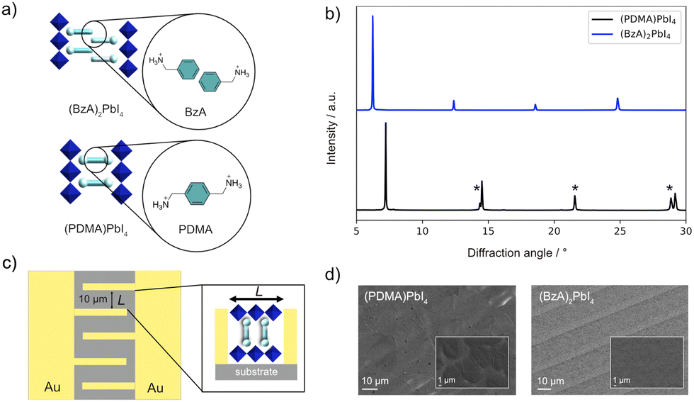 | ||
| Fig. 1 (a) Schematic of RP (top) and DJ (bottom) phases in this study with the corresponding (BzA, PDMA) spacer structures (cyan) and different alignments between the adjacent inorganic layers (blue). (b) X-ray diffraction patterns of (BzA)2PbI4 (blue) and (PDMA)PbI4 (black). Here * corresponds to higher-order (h00) reflections.24–28 UV-vis absorption spectra of the films are shown in Fig. S1 (ESI†) with XRD patterns showing comparable structures of the materials in films and devices (ESI†). (c) Schematic representation of the electrode substrate (quartz) used for electrical measurements. Inset: Graphic illustration of a DJ perovskite placed between two electrodes. (d) SEM images of (PDMA)PbI4 and (BzA)2PbI4 thin films deposited on the substrates with interdigitated contacts (5 μm wide gold fingers are visible in the image). Insets represent the SEM images of the films at higher magnification (the corresponding scale bars are shown on the images). | ||
In this work, we investigate the electrochemical response of RP and DJ layered hybrid perovskite model systems based on comparable aromatic spacer moieties, namely benzylammonium (BzA) and 1,4-phenylenedimethylammonium (PDMA) in (BzA)2PbI4 and (PDMA)PbI4 compositions, respectively. We apply electrochemical techniques to elucidate the effect of dimensionality and interlayer spacing on mixed conductivity in layered hybrid perovskites of interest to optoelectronics.
Results
This study focuses on representative layered hybrid perovskites based on n = 1 compositions comprising BzA, which crystallize in RP type (BzA)2PbI4 structure, and PDMA spacers, forming DJ (PDMA)PbI4 perovskites (Fig. 1a and b).24–28 The preparation is detailed in the Methods section of the ESI.†The structural properties of thin films were investigated by X-ray diffraction (XRD, Fig. 1b). XRD patterns of a (BzA)2PbI4 thin film deposited on glass substrates show (00l) reflection peaks, which indicate the presence of crystallites with perovskite layers that are oriented parallel to the substrate. Similarly, the most intense peaks of (PDMA)PbI4 films show (h00) Miller indices corresponding to the parallel orientation of perovskite layers with respect to the substrate (Fig. 1b). In addition, there are (0kl) reflections coming from perpendicularly orientated perovskite layers with lower intensity, implying that the dominant crystallite orientation is parallel to the substrate with a larger d-spacing for RP as compared to DJ phases.26 The spacers affect the domain sizes for the corresponding phases in thin films with dimensions in the order of 10–20 μm for DJ and hundreds of nanometres for the RP thin films.24–30 This is relevant for the electrochemical measurements, which were based on the device architecture with interdigitated gold contacts (Fig. 1c). Considering the preferential orientation of the crystallites,24–28 the in-plane conductivity is expected to dominate the measured response (Fig. 1c, inset). The films deposited on quartz substrates with interdigitated gold contacts were assessed by scanning electron microscopy (SEM), evidencing that both (PDMA)PbI4 and (BzA)2PbI4 (Fig. 1d) feature compact uniform morphology.
The electrical properties were measured by galvanostatic polarization and impedance spectroscopy experiments (detailed in the Methods section). Direct current (DC) measurements performed in an argon atmosphere at 60 °C in the dark display significant polarization in the thousands of seconds timescale, as evidenced by the increase in measured voltage as a function of time for (PDMA)PbI4 and (BzA)2PbI4 films (Fig. 2). This observation is consistent with a significant ionic conductivity, similar to previous results obtained for 3D perovskites.31–35 The electronic conductivity extracted from the long time scale resistance, assuming ion-blocking behaviour at the perovskite–gold interface, is on the order of 2–5 × 10⁻¹¹ S cm−1 for both DJ and RP systems.24–28 Accurate evaluation of the ionic conductivity is challenging under these conditions; the impedance spectra do not show a clear high-frequency feature, complicating the fit of equivalent circuit models.34,35 We estimate upper limits to the ionic conductivity in the range of 10−11–10−10 S cm−1 by fitting both bulk and grain boundary elements (two R–C in series) to the high-frequency feature of the impedance to extract the total conductivity. We also account for the analysis of the gap width L (Fig. 1c) dependence of the electrical response for these estimates.34 This highlights the presence of an interfacial resistance for the DJ film measured under argon, which becomes negligible when the sample is measured under fixed iodine partial pressure (P(I2)) (see Supplementary discussion and Fig. S2, ESI†). We can, thus, confidently assign such estimates to the bulk properties.
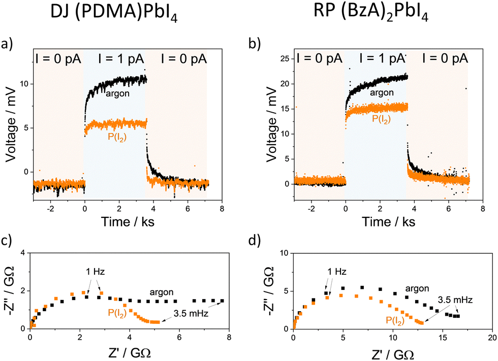 | ||
| Fig. 2 Galvanostatic polarization measurements performed on horizontal devices with (a) (PDMA)PbI4 and (b) (BzA)2PbI4 thin films in an argon atmosphere and under iodine atmosphere (P(I2) = 7 × 10⁻⁷ bar; argon carrier gas) at 60 °C in the dark. Impedance spectra collected under analogous conditions are shown in (c) for the DJ and (d) for the RP film. | ||
Dimensionality reduction has a clear and substantial effect on electrical properties, in that both RP and DJ samples have several orders of magnitude lower electronic conductivities (σeon) in the dark in comparison to MAPbI3, for which values on the order of 10−9–10−6 S cm−1 were previously reported.11,32–37 The lower electronic conductivity of layered hybrid perovskites is likely due to their larger bandgap and charge carrier confinement, which could further decrease the concentration of electronic charge carriers. These effects would be lower in quasi-2D perovskites based on nominal compositions with n > 1, as their structural and optoelectronic properties approach those of 3D perovskites. The reduced ionic conductivity could also be associated with multiple factors, including defect formation energy, anisotropy effects, or ion migration energy barrier, which will be discussed later.
The conductivity of mixed conductors can be modulated by changing their stoichiometry in situ. This has been experimentally demonstrated for hybrid perovskites by measuring their electrical properties under fixed iodine partial pressure.2 When RP and DJ samples are exposed to iodine partial pressure (7 × 10⁻⁷ bar), changes in the polarization curves and in the shape of the impedance spectra of both (PDMA)PbI4 (Fig. 2a and c) and (BzA)2PbI4 (Fig. 2b and d) are evidenced compared to the argon case. As a result, larger values of the electronic conductivity and shorter time constants in the DC measurements are found for the high P(I2). To probe the conduction type and gain insights into the defect chemistry of these systems, partial conductivities in (PDMA)PbI4 and (BzA)2PbI4 are analysed as a function of iodine partial pressure, in the range from 3.5 × 10⁻⁷ to 1.4 × 10⁻⁵ bar (Fig. 3a and b), using DC and AC measurements performed after equilibration at each condition. Upon increasing iodine partial pressure, the electronic conductivity increases with a slope of approximately 0.5–0.6 in both RP and DJ compounds (dashed lines in Fig. 3a and b), indicating a p-type character for the electronic conduction.36 Such change in conductivity is only partially reversible, as highlighted by the data points referring to the first scan. Specifically, a larger value of σeon is retained when returning the initial P(I2) value. When performing a second forward and reverse scan in P(I2), we find a much more reversible trend of the electronic conductivity, however with a reduced slope of 0.35–0.4, for both samples (see protocol for the experiment in the Methods section of the ESI†). Such observation could be consistent with some reactivity of the sample to iodine that irreversibly changes its properties. The ionic conductivities of the two thin films undergo a less pronounced change when varying P(I2), with a slight decrease for the DJ sample and a more significant increase for the RP sample. The overall slopes recorded for the ionic conductivities of the DJ and RP samples are on the order of –0.16 and 0.33, respectively. We expect a large error associated with the estimated ionic conductivity. For the DJ sample, the slightly negative slope extracted for the ionic conductivity data is consistent with the intrinsic behaviour of the film and provides confidence in the interpretation of the data. On the other hand, the positive slope extracted for the RP sample cannot be easily explained and it might point to a more complex electronic and ionic transport mechanism in the film, and accordingly, to a possible overestimation of the ionic conductivity in our analysis (further discussion on possible defect chemical models relevant to these 2D systems can be found in the Sections 2 and 3 of the ESI†).
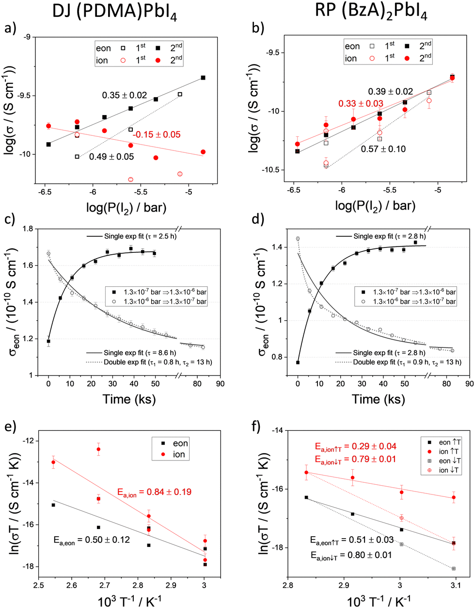 | ||
| Fig. 3 (a) and (b) Electronic and ionic conductivities of (a) (PDMA)PbI4 and (b) (BzA)2PbI4. The positive slope of σionvs. P(I2) recorded for the RP film points to possible inaccuracy in its estimation (see text). (c) and (d) Electronic conductivity as a function of time extracted from a series of DC polarization measurements performed during the equilibration of (PDMA)PbI4 and of (BzA)2PbI4 based devices when P(I2) is adjusted from 1.3 × 10⁻⁷ to 1.3 × 10⁻⁶ bar and when the reverse step is applied. The carrier gas is argon and the sample temperature 60 °C. (e) and (f) Arrhenius plots of (PDMA)PbI4 (e) and (BzA)2PbI4 (f) for electronic (eon, black) and ionic (ion, red) charge carrier transport obtained from conductivity measurements performed in the dark under P(I2) 6.9 × 10⁻⁷ bar atmosphere. In the legend label, an upward and a downward arrow are used to indicate the temperature scan used for collecting the data points to describe the increasing and decreasing temperature, respectively. | ||
The kinetics of iodine exchange with the films was analyzed to probe the effect of dimensionality reduction on the incorporation/excorporation of halogen. The evolution in the electronic conductivity as a function of time after switching the iodine partial pressure in the measuring cell was recorded by performing a sequence of DC polarization measurements. Even though layered perovskites are more resistive than MAPbI3 and iodine incorporation is expected to occur across layers separated by insulating organic spacers in the sample architecture used (Fig. 1c), the equilibration kinetics show a relatively short characteristic time constant of 2–10 h (Fig. 3c and d, data fitted with a single exponential function; fit of a double exponential also shown for the iodine excorporation). Note that the differences in time constant between the incorporation and excorporation reactions can be explained by the relatively large steps in P(I2) value used here. These were selected to detect large enough changes in conductivity. The time scale of the iodine exchange, which is comparable to the one recorded for MAPbI3 under similar conditions,38 would not point to bulk diffusion as a limiting factor to the overall reaction. It is possible that in the 2D systems, the surface exchange may be the limiting step to the exchange reaction,39 although anisotropy effects make the comparison with the polarization timescale difficult. It is also interesting that similar kinetics recorded for DJ and RP samples refer to two different film compositions but also different surface morphologies. The relatively efficient surface reaction step in the studied DJ and RP systems points to the possible diffusion of iodine within the perovskite layers, such as through grain boundaries and other high dimensional defects in the films (Fig. S3, ESI†), as well as in regions where layer orientations that are not parallel to the substrate are present, which may be more likely for DJ films. The observed halogen exchange at the solid/gas interface for both RP and DJ films could potentially undermine their use for passivation in perovskite solar cells. As noted above, it is striking that the P(I2) dependence of the electronic conductivity in these films is less pronounced than the one reported for MAPbI3 after exposure to large iodine partial pressures (in the intrinsic region, σ ∝ P(I2)1/2, see Section 4 of the ESI†). Indeed, if some parts of the films (possibly the region far from the solid–gas interface) were less accessible due to the layered nature of the compounds, the exchange of iodine would induce a <1/2 slope in the conductivity trend vs. P(I2). As a result, such “retardation” in iodine exchange would provide an enhanced encapsulation capability, compared with the case of a 3D perovskite film that is fully exposed to the gas phase, while not entirely resolving the issue of halogen exchange. Future investigations are needed to ascertain such a scenario.
To assess the activation energies for ion migration, we analysed the temperature dependence of the ionic and electronic conductivities based on the relation in eqn 1.
 | (1) |
To gain further insights into the effects on the thermal stability of these 2D materials, which is relevant to their application,29 DJ and RP thin films were analysed using in situ temperature-dependent XRD in the dark under a nitrogen atmosphere. By tracking the intensities of diffraction peaks over time (Fig. 4a and b) we reveal that (BzA)2PbI4 (002) and (004) peaks slightly change at 90–100 °C, indicating minor layered structure disruption in this temperature range (Fig. S6a, ESI†). Moreover, a peak at 6.9° appears during the measurement and becomes more intense with time, which we interpret in terms of layered structure conversion to another intermediate phase occurring for the BzA-based RP sample for temperatures greater than ∼90 °C (Fig. S6c, ESI†). At higher temperatures, this phase is transformed into PbI2 (Fig. 4b). We note that (BzA)2PbI4 films show no decomposition (Fig. S6b, ESI†) when kept at 60 °C for up to 42 days, indicating that no significant structural changes occurred during the electrical characterization performed at such temperature.44 We note that temperature stability of the RP film would be expected in the temperature range used to collect the data (Fig. 3f, 50–80 °C) based on this analysis. The recorded irreversible conductivity trend points to changes in the material occurring already at temperatures in the order of 80 °C, which are however not detectable from our XRD study. Importantly, the data (Fig. 3f) were collected under a fixed P(I2), which may lead to slight differences in the thermochemical stability of the material. On the contrary, the (PDMA)PbI4 samples show remarkably better thermal stability as no degradation is observed in the temperature range up to 150 °C (Fig. 4a and Fig. S6d, ESI†), corroborating enhanced stabilities of DJ as compared to RP phases.
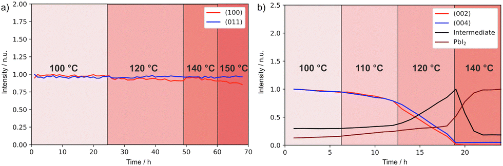 | ||
| Fig. 4 XRD peak intensity change over time and of (a) (PDMA)PbI4 sample in the temperature range of 100–150 °C and of (b) (BzA)2PbI4 sample in the temperature range of 100–140 °C in a nitrogen atmosphere. The peak intensities were normalized by taking the initial values at starting temperatures (Fig. S6c, ESI†). | ||
This difference in thermal stability between the DJ and the RP compounds can be related to the van der Waals gap between organic layers in RP hybrid halide perovskites. Weakly bound spacer molecules might be more susceptible to thermal stress, which could eventually induce material degradation. In contrast, bifunctional spacers in DJ analogues do not form a van der Waals gap between adjacent perovskite layers, thereby featuring shorter I…I interlayer distances, which can be relevant for their thermal stability.29 Consequently, the more rigid structure provides improved stability at high temperatures26,29,51 as corroborated by the results. This makes DJ perovskites potentially more promising materials for designing protection and passivation layers in perovskite solar cells.
Conclusions
We investigate the electrochemical properties of (PDMA)PbI4 and (BzA)2PbI4 layered perovskite thin films representing DJ and RP phases, respectively. We find that these materials are mixed ionic-electronic conductors, with ionic conductivities on the order of 10−10 S cm−1 in the dark close to equilibrium at 60 °C in the direction parallel to the perovskite layers, about 2–4 orders of magnitude lower compared to 3D hybrid perovskites. This result emphasizes the lowering of ion transport by dimensional reduction. The similar conductivity values measured for DJ and RP samples indicate that the chemical nature of the spacer is of minor influence on the conduction properties. Exposure of the samples to atmospheres with fixed iodine partial pressure revealed iodine incorporation and excorporation rates comparable to MAPbI3. Increased electronic conductivity on increasing iodine partial pressure indicates p-type conduction in both the RP and DJ systems. Temperature-dependent conductivity measurements indicate higher activation energies of ion migration in the 2D phases compared to 3D hybrid perovskites, consistent with the suppressed ionic conductivity. We demonstrated thermal stability up to 150 °C for (PDMA)PbI4 DJ samples. This is not matched by (BzA)2PbI4 films, which suffer from degradation detected with XRD measurements at temperatures above ∼100 °C, and irreversible changes in conductivity already at temperatures ∼80 °C. This is possibly due to weak van der Waals interactions in the spacer layer. We conclude that, despite their significantly reduced ion migration compared to 3D systems, layered perovskite compositions based on phenyl-derived aromatic spacers still allow for detectable halogen exchange with the gas phase. While these findings partially challenge the current perspective on the role of these materials in stabilizing perovskite devices, they stimulate further investigations to realize their potential through a careful understanding of layer stacking and surface reactions. These questions may become more critical for quasi-2D perovskites (n > 1) due to inherited features from 3D perovskites, with broad implications in perovskite materials and devices.Author contributions
The manuscript was written by A. D. with the support of D. M. and J. V. M., whereas J. V. M., M. G. and J. M. conceptualized the study. A. D. prepared the samples and conducted the analysis with the support of D. M., Y-R. W. and M. J. while J. V. M. and D. M. supervised A. D., and J. M. and M. G. directed the project. All authors have approved the final manuscript.Data availability
Data can be accessed at the DOI:10.5281/zenodo.11123730 and it is available under the license CC-BY-4.0.Conflicts of interest
There are no conflicts to declare. Open Access funding provided by the Max Planck Society.Acknowledgements
A. D., D. M., J. M. and M. G. acknowledge the support from the Max Planck Society and the Max-Planck/EPFL Center. J. V. M. is grateful for the Swiss National Science Foundation grant no. 193174.Notes and references
- W. Tress, J. Phys. Chem. Lett., 2017, 8, 3106–3114 CrossRef CAS PubMed.
- A. Senocrate and J. Maier, J. Am. Chem. Soc., 2019, 141, 8382–8396 CrossRef CAS.
- R. Wang, M. Mujahid, Y. Duan, Z.-K. Wang, J. Xue and Y. Yang, Adv. Funct. Mater., 2019, 29, 1808843 CrossRef CAS.
- M. H. Futscher and J. V. Milić, Front. Energy Res., 2021, 9, 629074 CrossRef.
- J. Bisquert and E. J. Juarez-Perez, J. Phys. Chem. Lett., 2019, 10, 5889–5891 CrossRef CAS.
- A. Enocrate, E. Kotomin and J. Maier, Helv. Chim. Acta, 2020, 103, e2000073 CrossRef.
- Y. Park and J.-S. Lee, J. Phys. Chem. Lett., 2022, 13, 5638–5647 CrossRef CAS PubMed.
- K. Sakhatskyi, R. A. John, A. Guerrero, S. Tsarev, S. Sabisch, T. Das, G. J. Matt, S. Yakunin, I. Cherniukh, M. Kotyrba, Y. Berezovska, M. I. Bodnarchuk, S. Chakraborty, J. Bisquert and M. V. Kovalenko, ACS Energy Lett., 2022, 10, 3401–3414 CrossRef PubMed.
- J. Bisquert and A. Guerrero, J. Phys. Chem. Lett., 2022, 13, 3789–3795 CrossRef CAS PubMed.
- D. W. Ferdani, S. R. Pering, D. Ghosh, P. Kubiak, A. B. Walker, S. E. Lewis, A. L. Johnson, P. J. Baker, M. S. Islam and P. J. Cameron, Energy Environ. Sci., 2019, 12, 2264–2272 RSC.
- Y. Yuan and J. Huang, Acc. Chem. Res., 2016, 49, 286–293 CrossRef CAS.
- Y. Lin, Y. Bai, Y. Fang, Q. Wang, Y. Deng and J. Huang, ACS Energy Lett., 2017, 2, 1571–1572 CrossRef CAS.
- X. Xiao, J. Dai, Y. Fang, J. Zhao, X. Zheng, S. Tang, P. N. Rudd, X. C. Zeng and J. Huang, ACS Energy Lett., 2018, 3, 684–688 CrossRef CAS.
- D. B. Mitzi, J. Chem. Soc., Dalton Trans., 2001, 1, 1–12 RSC.
- B. Saparov and D. B. Mitzi, Chem. Rev., 2016, 116, 4558–4596 CrossRef CAS PubMed.
- G. Grancini and M. K. Nazeeruddin, Nat. Rev. Mater., 2019, 4, 4–22 CrossRef CAS.
- L. Mao, S. M. L. Teicher, C. C. Stoumpos, R. M. Kennard, R. A. DeCrescent, G. Wu, J. A. Schuller, M. L. Chabinyc, A. K. Cheetham and R. Seshadri, J. Am. Chem. Soc., 2019, 141, 19099–19109 CrossRef CAS PubMed.
- X. Li, J. M. Hoffman and M. G. Kanatzidis, Chem. Rev., 2021, 121, 2230–2291 CrossRef CAS PubMed.
- P. S. Mathew, J. T. DuBose, J. Cho and P. V. Kamat, ACS Energy Lett., 2021, 6, 2499–2501 CrossRef CAS.
- Z. Chen, H. Xue, G. Brocks, P. A. Bobbert and S. Tao, ACS Energy Lett., 2023, 8, 943–949 CrossRef CAS PubMed.
- Y.-R. Wang, A. Senocrate, M. Mladenović, A. Dučinskas, G. Y. Kim, U. Rothlisberger, J. V. Milić, D. Moia, M. Grätzel and J. Maier, Adv. Energy Mater., 2022, 12, 2200768 CrossRef CAS.
- J. Cho, J. T. DuBose, A. N. T. Le and P. V. Kamat, ACS Mater. Lett., 2020, 2, 565–570 CrossRef CAS.
- K. Mao, W. Ke, L. Pedesseau, Y. Wu, C. Katan, J. Even, M. R. Wasielewski, C. C. Stoumpos and M. G. Kanatzidis, J. Am. Chem. Soc., 2018, 140, 3775–3783 CrossRef PubMed.
- Y. Li, J. V. Milić, A. Ummadisingu, J.-Y. Seo, J.-H. Im, H.-S. Kim, Y. Liu, M. I. Dar, S. M. Zakeeruddin, P. Wang, A. Hagfeldt and M. Grätzel, Nano Lett., 2018, 19, 150–157 CrossRef PubMed.
- M. C. Gélvez-Rueda, P. Ahlawat, L. Merten, P. Jahanbakhshi, M. Mladenović, A. Hinderhofer, M. I. Dar, Y. Li, A. Dučinskas, B. Carlsen, W. Tress, A. Ummadisingu, S. M. Zakeeruddin, F. Schreiber, A. Hagfeldt, U. Rothlisberger, F. C. Grozema, J. V. Milić and M. Graetzel, Adv. Funct. Mater., 2020, 30, 2003428 CrossRef.
- A. Dučinskas, G. Y. Kim, D. Moia, A. Senocrate, Y.-R. Wang, M. A. Hope, A. Mishra, D. J. Kubicki, M. Siczek, W. Bury, T. Schneeberger, L. Emsley, J. V. Milić, J. Maier and M. Grätzel, ACS Energy Lett., 2020, 6, 337–344 CrossRef.
- A. Dučinskas, G. C. Fish, M. A. Hope, L. Merten, D. Moia, A. Hinderhofer, L. C. Carbone, J.-E. Moser, F. Schreiber, J. Maier, J. V. Milić and M. Grätzel, J. Phys. Chem. Lett., 2021, 12, 10325–10332 CrossRef PubMed.
- A. Q. Alanazi, M. H. Almalki, A. Mishra, D. J. Kubicki, Z. Wang, L. Merten, F. T. Eickemeyer, H. Zhang, D. Ren, A. Alyamani, Y. H. Albrithen, A. Albadri, M. H. Alotaibi, A. Hinderhofer, S. M. Zakeeruddin, F. Schreiber, A. Hagfeldt, L. Emsley, J. V. Milić and M. Graetzel, Adv. Funct. Mater., 2021, 31, 2101163 CrossRef CAS.
- Z. Lai, F. Wang, Y. Meng, X. Bu, X. Kang, Q. Quan, W. Wang, C. Liu, S. Yip and J. C. Ho, Adv. Opt. Mater., 2021, 9, 2101523 CrossRef CAS.
- C. Lermer, A. Senocrate, I. Moudrakovski, T. Seewald, A.-K. Hatz, P. Mayer, F. Pielnhofer, J. A. Jaser, L. Schmidt-Mende, J. Maier and B. V. Lotsch, Chem. Mater., 2018, 30, 6289–6297 CrossRef CAS.
- T.-Y. Yang, G. Gregori, N. Pellet, M. Grätzel and J. Maier, Angew. Chem., Int. Ed., 2015, 54, 7905–7910 CrossRef CAS.
- A. Senocrate, I. Moudrakovski, G. Y. Kim, T.-Y. Yang, G. Gregori, M. Grätzel and J. Maier, Angew. Chem., Int. Ed., 2017, 129, 7863–7867 CrossRef.
- G. Y. Kim, A. Senocrate, Y.-R. Wang, D. Moia and J. Maier, Angew. Chem., 2021, 133, 833–839 CrossRef.
- D. Moia, M. Jung, Y.-R. Wang and J. Maier, Phys. Chem. Chem. Phys., 2023, 25, 13335–13350 RSC.
- D. Moia and J. Maier, ACS Energy Lett., 2021, 6, 1566–1576 CrossRef CAS.
- A. Senocrate, T.-Y. Yang, G. Gregori, G. Y. Kim, M. Grätzel and J. Maier, Solid State Ionics, 2018, 321, 69–74 CrossRef CAS.
- P. V. Kamat and M. Kuno, Acc. Chem. Res., 2021, 54, 520–531 CrossRef CAS.
- A. Senocrate, T. Acartürk, G. Y. Kim, R. Merkle, U. Starke, M. Grätzel and J. Maier, J. Mater. Chem. A, 2018, 6, 10847–10855 RSC.
- A. Senocrate, I. Spanopoulos, N. Zibouche, J. Maier, M. S. Islam and M. G. Kanatzidis, Chem. Mater., 2021, 33, 719–726 CrossRef CAS.
- A. Senocrate, I. Moudrakovski, T. Acartürk, R. Merkle, G. Y. Kim, U. Starke, M. Grätzel and J. Maier, J. Phys. Chem. C, 2018, 122, 21803–21806 CrossRef CAS.
- M. H. Futscher, J. M. Lee, L. McGovern, L. A. Muscarella, T. Wang, M. I. Haider, A. Fakharuddin, L. Schmidt-Mende and B. Ehrler, Mater. Horiz., 2019, 6, 1497–1503 RSC.
- L. Muscarella, A. Dučinskas, M. Dankl, M. Andrzejewski, N. P. M. Casati, U. Rothlisberger, J. Maier, M. Graetzel, B. Ehrler and J. V. Milić, Adv. Mater., 2022, 34, 202108720 Search PubMed.
- L. McGovern, M. H. Futscher, L. A. Muscarella and B. Ehrler, J. Phys. Chem. Lett., 2020, 11, 7127–7132 CrossRef CAS PubMed.
- B. Conings, J. Drijkoningen, N. Gauquelin, A. Babayigit, J. D’Haen, L. D’Olieslaeger, A. Ethirajan, J. Verbeeck, J. Manca, E. Mosconi, F. D. Angelis and H.-G. Boyen, Adv. Energy Mater., 2015, 5, 1500477 CrossRef.
- J. Haruyama, K. Sodeyama, L. Han and Y. Tateyama, J. Am. Chem. Soc., 2015, 137, 10048–10051 CrossRef CAS PubMed.
- R. García-Rodríguez, D. Ferdani, S. Pering, P. J. Baker and P. J. Cameron, J. Mater. Chem. A, 2019, 7, 22604–22614 RSC.
- S. Meloni, T. Moehl, W. Tress, M. Fccaron, M. Saliba, Y. H. Lee, Y. P. Gao, M. K. Nazeeruddin, S. M. Zakeeruddin, U. Rothlisberger and M. Graetzel, Nat. Commun., 2016, 7, 10334 CrossRef CAS PubMed.
- R. A. D. Souza and D. Barboni, Chem. Commun., 2019, 55, 1108–1111 RSC.
- S. Tan, I. Yavuz, N. De Marco, T. Huang, S.-J. Lee, C. S. Choi, M. Wang, S. Nuryyeva, R. Wang, Y. Zhao, H.-C. Wang, T.-H. Han, B. Dunn, Y. Huang, J.-W. Lee and Y. Yang, Adv. Mater., 2020, 32, 1906995 CrossRef CAS PubMed.
- A. Mahapatra, Phys. Chem. Chem. Phys., 2020, 22, 11467–11573 RSC.
- S. Ahmad, P. Fu, S. Yu, Q. Yang, X. Liu, X. Wang, X. Wang, X. Guo and C. Li, Joule, 2019, 3, 794–806 CrossRef CAS.
Footnote |
| † Electronic supplementary information (ESI) available. See DOI: https://doi.org/10.1039/d4tc01010h |
| This journal is © The Royal Society of Chemistry 2024 |