
 Open Access Article
 This Open Access Article is licensed under a Creative Commons Attribution-Non Commercial 3.0 Unported Licence
Beyond the horizons of graphene: xenes for energy applications
Sumon
Santra†
 ,
Anuraag
Ghosh†
,
Bishwajit
Das†
,
Shibam
Pal†
,
Saikat
Pal†
* and
Ashadul
Adalder†
*
,
Anuraag
Ghosh†
,
Bishwajit
Das†
,
Shibam
Pal†
,
Saikat
Pal†
* and
Ashadul
Adalder†
*
Department of Industrial Chemistry & Applied Chemistry, Ramakrishna Mission Vidyamandira, Belur Math, Howrah 711202, India. E-mail: Saikatpal7200@gmail.com; iamashadul@gmail.com
First published on 9th May 2024
Abstract
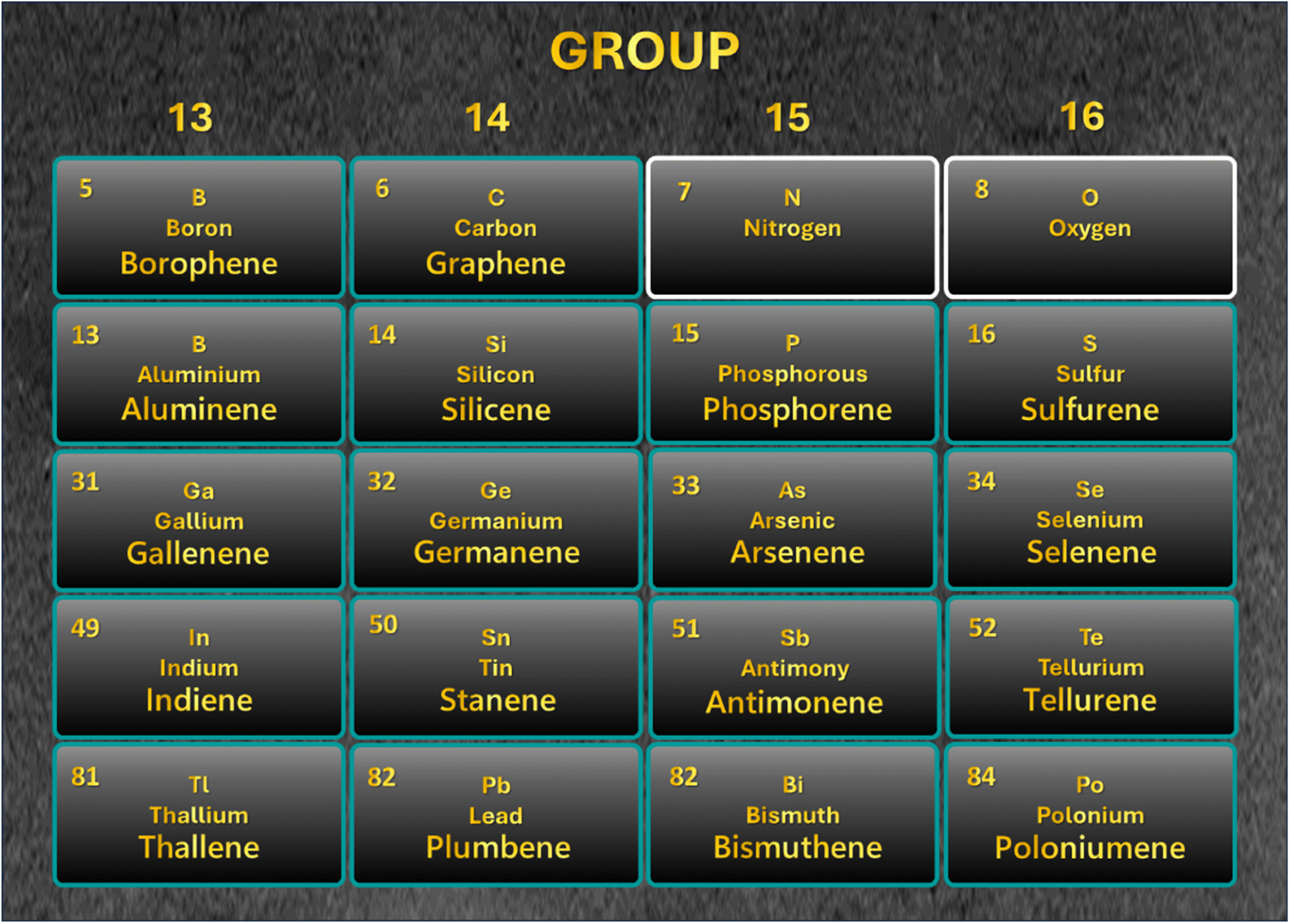
Almost two decades have passed since the discovery of graphene in 2004, which has revolutionized the world with its diverse applications. One application field is devoted to the future of energy materials, which is possible due to the various well-suited properties of graphene. This development is not limited to carbon-based materials. In the last decade, different new 2D materials similar to graphene were fabricated, having potential to be implemented as catalysts, supercapacitors, and batteries. These materials include mono-elemental 2D materials in groups 13, 14, 15, and 16 of the periodic table. Specifically, borophene, aluminene, gallenene, indiene, and thallene from group 13; graphene, silicene, germanene, stanene, and plumbene from group 14; phosphorene, arsenene, antimonene, and bismuthene from group 15; and sulfurene, selenene, tellurene, and poloniumene from group 16. Herein, we emphasize the general properties of these materials and the possibility of using them in energy applications based on their properties. This work will shed light on the future prospect of using mono-elemental 2D materials and how they may be better alternatives to graphene-based systems.
 Sumon Santra | Sumon Santra obtained his BSc in Industrial Chemistry from Ramakrishna Mission Vidyamandira College, under Calcutta University, India, and is currently pursuing his MSc degree in Applied Chemistry in the same department. He is currently working in the field of materials science for applications in electrocatalysis. His current research interest focuses on electrocatalytic HER, NRR, NO3RR, and CO2RR. |
 Anuraag Ghosh | Anuraag Ghosh obtained his BSc in Chemistry from Gurudas College, under Calcutta University, and is currently pursuing his MSc degree in Applied Chemistry at Ramakrishna Mission Vidyamandira, under Calcutta University, India. Currently, he is a visiting industrial project trainee in Himadri Speciality Chemical Ltd. |
 Bishwajit Das | Biswajit Das obtained his BSc in Chemistry from Dinabandhu Andrews College, under University of Calcutta, India and is currently pursuing an MSc in Applied Chemistry from Ramakrishna Mission Vidyamandira, affiliated to University of Calcutta, India. His research interests include application-oriented polymer designing and nanomaterial studies. At present, he is a visiting project trainee in IISER Kolkata in the field of ‘thio-ene’ type polymer system. |
 Shibam Pal | Shibam Pal obtained his BSc in Chemistry from Nabadwip Vidyasagar College, under University of Kalyani and presently pursuing MSc in Applied Chemistry from Ramakrishna Mission Vidyamandira, affiliated to University of Calcutta, India. Currently, he is a visiting industrial project trainee in PMC Rubber Chemicals Pvt Ltd. |
 Saikat Pal | Saikat Pal received his BSc degree in Industrial Chemistry in 2022 and is currently pursuing an MSc degree in Applied Chemistry from Ramakrishna Mission Vidyamandira, Calcutta University, India. He is currently working in materials science in the field of electrocatalysis and energy storage devices applications. His current research is focused in electrocatalytic HER, OER and pseudocapacitive energy storage. |
 Ashadul Adalder | Ashadul Adalder received his Master's Degree (MSc) in Applied Chemistry from Ramakrishna Mission Vidyamandira, Calcutta University in 2018. Then, he graduated from IIT Bombay in 2020 with an M.Tech Degree in Metallurgical Engineering and Materials Science. He received the S S Bhatnagar Young Scientist Award (for Best Oral Presentation) from the Indian Chemical Society in 2022. He received the Best Paper Award in 2023, Organized by the Indian Photobiology Society, Kolkata, India. He was awarded MRSI Young Scientist at the “Young Scientist Colloquium 2023” organized by the Kolkata Chapter of Materials Research Society of India. He is currently working as a Senior Researcher in Dr Uttam Kumar Ghorai's group. His research focuses on electrochemical N2/CO2/NO3−/NO2−/NO fixation to value-added products, and also energy storage applications. |
Sustainability spotlightThis sustainable spotlight statement aims to highlight the revolutionary strides made by mono-elemental 2D materials from groups 13, 14, 15, and 16 of the periodic table. These pioneers include borophene and aluminene from group 13, and silicene, germanene, and stanene from group 14. In groups 15 and 16, we encounter phosphorene, arsenene, antimonene, and bismuthine from group 15, and sulfurene, selenene, tellurene, and poloniumene from group 16, each holding unique properties that open avenues for applications in the realm of energy. Our emphasis was not only on delineating the inherent properties of these mono-elemental 2D materials but also illuminating their potential for transformative energy applications. As catalysts, supercapacitors, and components of batteries, these materials stand as beacons of innovation, offering new possibilities beyond the capabilities of graphene-based systems. Through this work, we aspire to unveil the untapped potential of these 2D materials, presenting them as compelling alternatives that can redefine the future of energy technologies. As we commemorate the one-year anniversary of this exploration, we look forward to the continued growth and sustainable contributions these materials can make in reshaping our energy landscape for years to come. |
1. Introduction
New materials are the energy boosters of the future. In the future, 2D materials will be dominant in energy and sustainable environmental applications and sustainable energy will be essential for a prosperous, green, and clean society. Specifically, renewable energy sources such as hydrogen fuel and solar power will be the solution for the next-generation wireless electrovoltaic era.1 Hence, continuous efforts are being devoted to improving our outlook with the development of novel materials. As materials become smaller, they are endowed with new properties. Going from the bulk to a sheet-like structure as thin as its stable physical limits permit creates new and fascinating properties totally altered from the bulk. At the stable conformational limit of these materials, they are referred to as 2-dimensional materials. The isolation of graphene from graphite as a 2D material was the greatest discovery in 2004 (Scheme 1).2 Since then, numerous 2D materials such as transition metal dichalcogenides, metal carbides, MXenes, and borides have joined the 2D family with excellent properties. After the development of silicene, there was a race in the development of ‘Xene systems,’ which are commonly known as ‘transgraphenes.’ In Xenes, ‘X’ refers to different elements.3–7 In the last decade, elemental 2D sheets have been developed in the form of borophene (boron), silicene (silicon), germanene (germanium), stanene (tin), phosphorene (phosphorus), etc. Among the 2D materials, graphene is the most extensively studied because of its exceptional metal-like electrical, thermal, electrochemical, optoelectronic, and biomedical properties, and quantum spin Hall effect8 at the 2D level. It must also be considered that graphene is a well-known carbon-based material. Also, beyond graphene, other materials have been investigated and well developed.9,10 The dazzling 2D materials are at the forefront of catalysis due to their three main properties of high specific surface area, mechanical properties, and thermal and electrical conductivity.11 They have the maximum possible surface-to-bulk ratio, facilitating the maximum number of active sites for catalytic processes, which are surface-active phenomena. Presently, the global view on clean catalysis is green catalysis, which is directly connected to the generation and utilization of hydrogen, such as HER, HOR, and CO2RR. The main aim of the present review is to compare the electrocatalytic12,13 and electrochemical performances14 of 2D materials with that of the well-established noble metal-based catalyst from both alternative and economical viewpoints. Supercapacitors are also an important class of energy storage devices, which can adapt to very fast charging and discharging due to their high power density. Our target material class applies to anode engineering to facilitate faster ion intercalation and double-layer formation at the electrode–electrolyte interface. In contrast to supercapacitors, batteries have a higher energy density than high power density. In this case, 2D nanosheets (silicene, germanene, stanene, phosphorene, arsenene, antimonene, and bismuthene, which are analogous to graphene) have been engineered to realize short diffusion paths and good conductivity and greater intercalating ion storage.15–17 These supreme classes of materials have been designed for energy storage applications due to their layered structure, well-defined geometry, and large surface area, while their superior intercalating ion accommodation capability makes them dominant. The large surface area takes part in electrostatic double-layer capacitance, wherein the defect position, edges, and reactive basal planes take part in the electrochemical redox capacitance, and here simultaneously, both electrostatic capacitance and redox capacitance improve the pseudocapacitance.18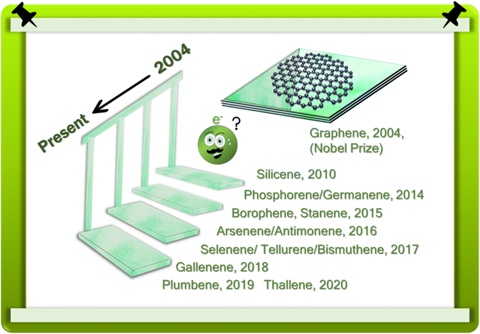 | ||
| Scheme 1 Advent of Xene-based development routes. | ||
In the past ten years, an array of novel 2D materials has emerged, sharing similarities with the much-acclaimed graphene. These materials show potential for applications such as catalysis, supercapacitors, and batteries,19 especially 2D materials found in groups 13, 14, 15, and 16 of the periodic table13 are promising (Fig. 1). We focus on the fundamental properties these materials and exploring their viability for energy-related functions, building on their inherent characteristics. This endeavour sheds light on the promising future prospects of integrating mono-elemental 2D materials, potentially offering a superior alternative to graphene-based systems.
 | ||
| Fig. 1 Schematic diagram of 2D materials and their energy-related applications. | ||
2. Materials
2.1 Borophene
Similar to graphene, borophene is a two-dimensional allotrope of boron. Precisely, it can be considered crystalline atomically monolayers of boron. Although its structure was theoretically predicted, the first monolayer borophene was produced in 2015 by Mannix et al.20 under ultrahigh vacuum condition on an Ag (111) substrate. The Ag substrate was first cleaned using argon sputtering, and the substrate was further annealed at 550 °C. Subsequently, boron was deposited using a boron rod on the substrate in the temperature range of 450 °C to 700 °C.20 It is obvious that the thermal evaporation and sputtering techniques are costly techniques, and the use of substrates severely limits their applications. Thus, in recent times, several other liquid-phase exfoliation techniques have been developed, which are comparatively economical. In the recent work by Ranjan et al. in 2019,21 they showed the possibility of synthesizing borophene in different solvents such as water, DMF, acetone, IPA, and ethylene glycol. This work gave insight into the effect of solvent on the synthesis of borophene. It was found that acetone and ethylene glycol resulted in the formation of monolayer borophene and DMF resulted in multilayer sheets, whereas other solvents resulted in smaller sheet sizes.22 If multilayer synthesis is considered, DMF-IPA mixed solvent results in the formation of a nanometer- to micrometer-scale sheet size using the liquid phase exfoliation technique.23 Similar to graphene oxide, borophene can also be synthesized via the Hummers' method. As a result of this oxygen defect, rich borophene can be obtained. Unlike graphene oxide, oxidized borophene is considered advantageous for use in charge storage applications.24In the X-ray diffraction characterization, the only observable difference between bulk boron powder and borophene is the disappearance of the XRD peak corresponding to the (003) and (012) planes in Fig. 2. This shows that exfoliation results in the loss of the plane orientations.26 The use of SEM and TEM further confirmed the crystal structure and size of borophene. It was found that borophene has a d-spacing value of 0.54 nm, which was observed to correspond to the (110) plane in the β-borophene structure.26Fig. 3 shows the STM images of the different borophene phases.21
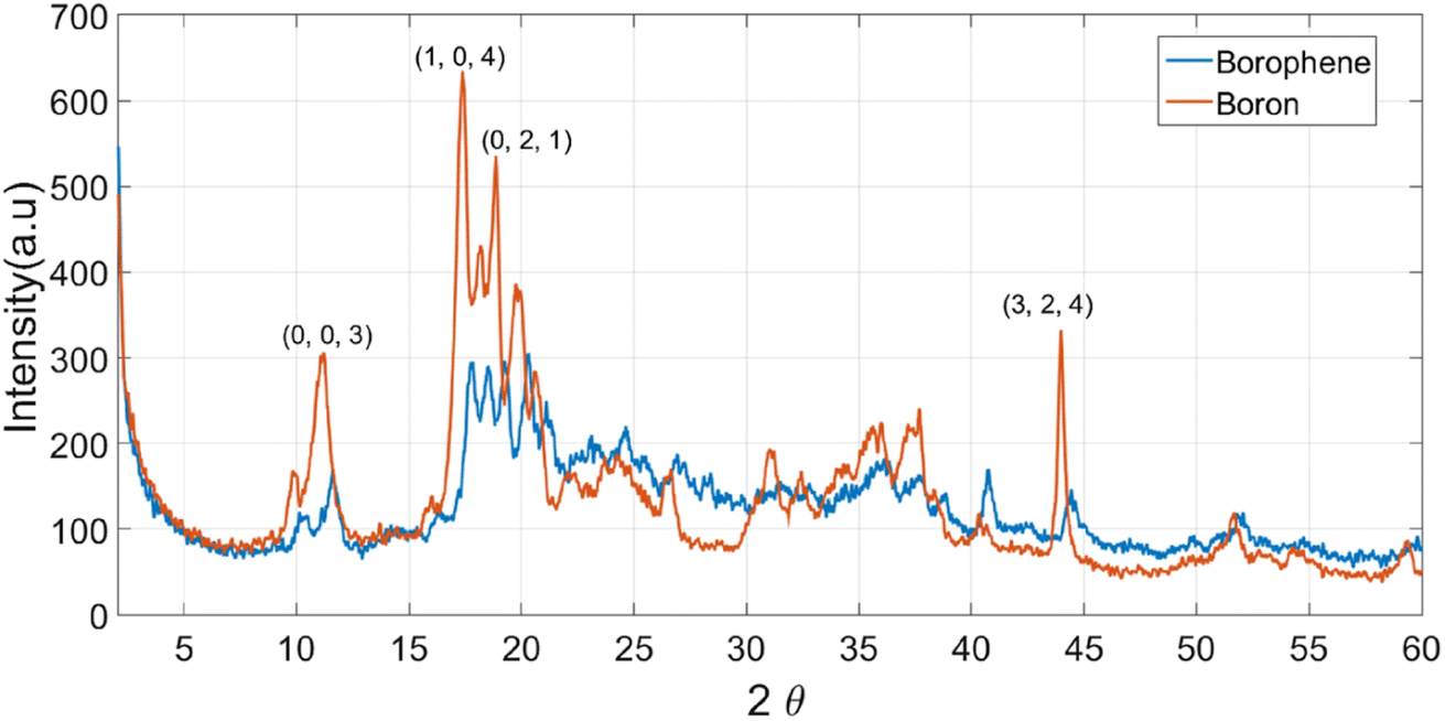 | ||
| Fig. 2 Comparative PXRD plot of boron and borophene, where it can be clearly distinguished that the diffraction peaks corresponding to the (003), (021) and (324) planes are minimalized in the borophene material. Reproduced from ref. 25, copyright 2022. | ||
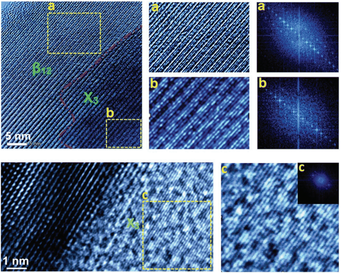 | ||
| Fig. 3 STM images of the different phases of borophene. Reproduced from ref. 21, copyright 2019. | ||
Borophene has been found to show metallic to semi-metallic character. The 2D Brillouin zone calculated in the study by Mannix et al. showed that borophene exhibited good electrical conductivity along the chain of the material.20 With the introduction of strain in the crystal structure, the electrical conductivity of the material also improved, which can serve as a new path in the development of a new class of superconductors. In the theoretical work by Xiao et al., they reported that in the pristine state, borophene superconducts at a Tc of about 19.0 K. However, with the introduction of tensile strain and hole doping, the Tc changed to 27.4 K and 34.8 K, respectively.27 Besides its proven anisotropic metallic character, borophene also demonstrates unique mechanical properties. In comparison, it has been found that borophene has a higher Young's modulus value compared to graphene, which is known as the strongest material.28 Borophene is not only mechanically strong but has also been found to be thermally stable at a temperature of around 400 °C.22 According to UV spectroscopy, the band gap of borophene was found to be near about 2.48 eV.22 However, unlike other 2D materials whose band gap can be modified by using engineering techniques such as functionalization, vacancy generation, and edge formation, borophene is inert. In graphene, the modification of its structure can have a direct effect on its band structure due to quantum confinement, whereas this does not happen in the case of borophene.29
2.2 Aluminene
“Aluminene,” an analogue of graphene, is a 2D material from group-III. Phonon dispersion and cohesive energy calculation showed that buckled and 8-Pmmn aluminene are energetically stable.30 To date, aluminene has not been synthesized experimentally, but theoretical calculations using the density functional theory predict the possibility of its existence with a crystal lattice such as graphene, borophene, or even phosphorene.31 At the time of calculation, the spin effect was considered for buckled aluminene and 8-Pmmn aluminene. However, no spin polarization was observed in both systems, indicating both buckled and 8-Pmmn systems are non-magnetic. Based on the DFT calculation, buckled and 8-Pmmn aluminene exhibit metallic character.30 Also, they behave like a metallic system due to the partial occupancies of their σ and π bands. Aluminene, the material investigated in this work, exists in four different structure forms, namely, planar, triangular, buckled, and puckered. The AA and AB stacking of two triangular layers generate puckered and buckled aluminene, respectively. Among them, buckled structures are the most stable.322.3 Gallenene
Gallenene is the latest addition to the 2D family, which is a monolayer of gallium along the (010) and (100) crystallographic directions, respectively.33 The monolayer of a(100)-gallenene has a honeycomb structure with a rectangular primitive unit cell. Alternatively, monolayer b(010)-gallenene resembles a zigzag rhombic lattice with lower symmetry than a(100)-gallenene.34 Atomically thin samples of gallenene can be obtained from the bulk alpha phase of gallium using solid-melt exfoliation at a low melting temperature. A Ga droplet is first heated to 50 °C on a hot plate to achieve uniform melting of the entire droplet. Subsequently, the temperature is reduced to 30 °C, which is slightly above the melting temperature of Ga. At this point, a clean Si/SiO2 wafer is brought into contact with the surface of the Ga droplet. The lower temperature of the SiO2-Ga interface solidifies the surface of Ga layers, which are then exfoliated on the SiO2 substrate. According to theoretical prediction, free-standing Ga is difficult to exfoliate, but the substrate stabilizes gallenene. The height profile of this gallenene sheet measured using atomic force spectroscopy revealed that its thickness is ∼4 nm, indicating that the film is about four to six layers thick.35 Due to its very low thermal conductivity together with very high electrical conductivity, gallenene is unique. Thus, gallenene can be used as a potential on-chip electrical connector or thermal barrier in devices. 2D gallenene strongly interacts with the substrate. Consequently, gallenene contacts can be used to transform MoS2 from a semiconductor to a metallic phase, resulting in better 2D contacts for devices. Also, gallenene provides excellent opportunities to explore its application as a 2D metal in plasmonics, sensors, and electrical contacts.352.4 Indiene
Indiene, which is a triangular single-layer phase of indium, is a large gap (∼120 meV) quantum spin Hall insulator stabilized on SiC (0001) substrates. Its specific structural and electronic properties produce distinct fingerprints in experimental surface characterization by electron microscopy, diffraction, and spectroscopy, thus providing an efficient metric for synthesizing large-scale, high-quality indiene on SiC.36 Indiene has been theoretically predicted to exist in three different monolayer polymorphs, i.e., puckered, planar and buckled indiene.37 It can be synthesized by molecular beam epitaxy, leading to the formation of high-quality indiene films, as characterized by surface science tools.38 The synthesis is initiated by sublimating the topmost Si atoms of the SiC (0001) substrate under a supporting Ar atmosphere, leaving a C-rich buffer layer called zero-layer graphene. In the cyclic process of indium deposition and subsequent annealing, the carbon layer is replaced with indium as a bonding partner to the substrate. The indium forms a bilayer below graphene immediately after the intercalation. By thermal removal of In, the indium bilayer is converted into monolayer indiene, pushing it into the QSHI phase.39 The planar indiene behaves as a metal with two Dirac cones at K points in the Brillouin zone. In the case of buckled indiene, it has a small indirect band gap of 0.97 eV and behaves as a semiconductor. With an increase in the number of layers, the semiconducting buckled indiene transforms into metallic.37 The scanning electron micrograph reveals an essentially flat surface sprinkled with scarcely distributed islands, whose number and size increase as the deposition time is tripled.2.5 Thallene
The last element in group-III to form a 2D-Xene system is thallene, which is built of atoms of the group-III element thallium (Tl). It has been reported that it is formed when a 2/3 monolayer of mobile Tl atoms on single-layer NiSi2 atop Si(111) substrate crystallizes upon cooling below 150 K with a honeycomb geometry.40 The synthesis of thallene includes the successive formation of a sandwich structure on an Si (111) substrate consisting of 2/3 monolayer of Tl atoms residing atop a single-layer NiSi2 and cooling the sample to a low temperature, allowing the Tl atoms to crystallize into a honeycomb lattice. The experiments were performed in a UHV Omicron MULTIPROBE system equipped with STM, LEED, and ARPES facilities. To prepare the Si (111) 7 × 7 surfaces, the Si (111) samples were first annealed in situ at 600 °C for several hours, and finally flashed at 1280 °C. Tl was evaporated from a Ta crucible, and Ni was deposited from an electron beam evaporator.40 Similar to graphene, thallene has a flat honeycomb structure, where every third lattice site is vacant, which is clearly seen in high-resolution STM images. A substrate fixes the Tl–Tl bond length in the thallene, which is equal to 3.84 Å, whereas in the case of bulk thallium or free-standing thallene, DFT calculations yielded an equilibrium Tl–Tl bond length of 3.03 Å.40 Its structure has a space group symmetry of P6/mmm.41 Thallene works as a semiconductor with an indirect gap of 420 meV, where the highest occupied band is formed by the Tl Pxy orbitals and the lowest unoccupied band is mostly composed of Pz orbitals.42 The structure of thallene is shown in the STM image in Fig. 4.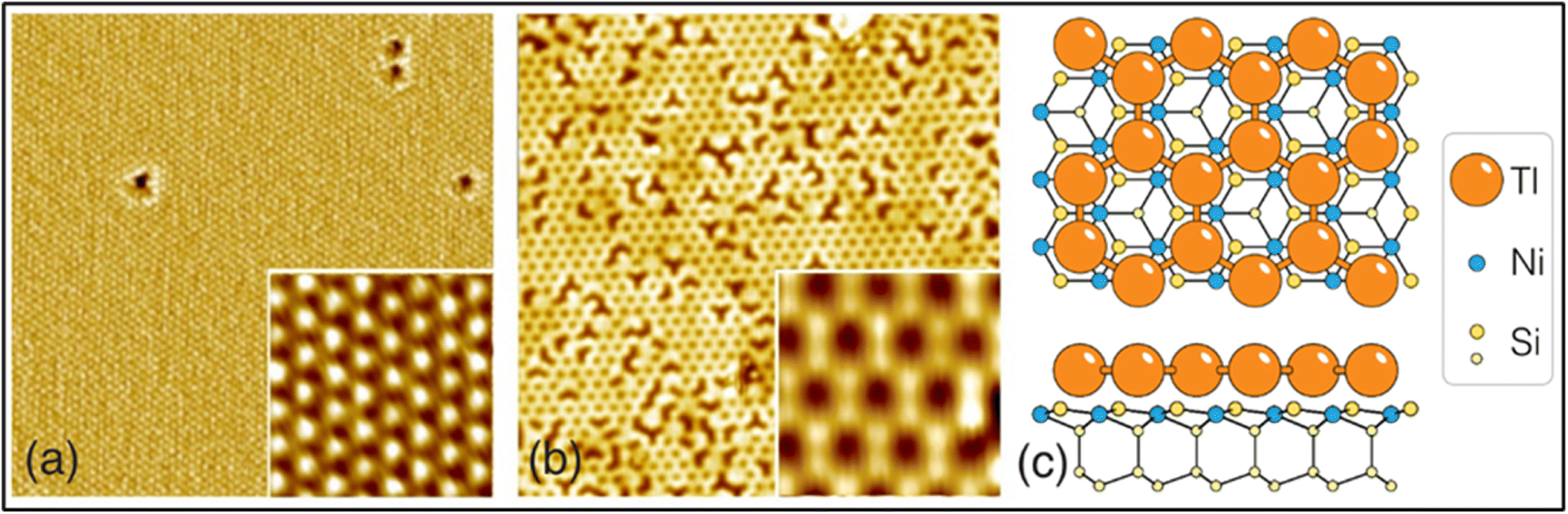 | ||
| Fig. 4 (a–c) STM image of thallene, where thallene is grown on the NiSi2/Si (111) surface. Reproduced from ref. 40, copyright 2020. | ||
2.6 Graphene
Graphene can be designated as a wonder material among the various classes of materials,43 and thus has been utilized in a wide variety of applications such as mechanical,44 electronic,45 optical,46 energy,47 environmental,48 and biomedical49,50 applications. Its development has not only been from an application point of view, where it has also been from an engineering aspect. In the last two decades, various graphene-based materials have been developed, such as graphene oxides, reduced graphene oxides, nanoribbons,45 and graphene quantum dots.51,52 Besides materials engineering, such as defects, doping, and composites, chemical modifications and functionalization have also been reported. This has given rise to complex systems such as graphane,53 graphyne,54 and partially reduced GO.55 After the discovery of graphene in 2004, various techniques were developed to synthesize 2D graphene.2 Firstly, graphene was synthesized as small flakes in the order of several microns from graphite by mechanical exfoliation. This method gives the highest pure-quality graphene, but considering large-scale production, it is synthesized from wafer-scale graphene.56 Graphene, similar to other nanomaterials, is synthesized by two processes, i.e., one is the top-down process, and the other is the bottom-up process. A bulk (graphite and graphite derivatives) material is used to synthesize the graphene in the top-down process. The top-down processes include mechanical exfoliation, reduction, and unzipping of CNT. Alternatively, in the bottom-up process, graphene is prepared by arranging atom by atom via a two-step process, i.e., nucleation and growth.General properties of graphene: graphene stands out for being tough, flexible, light weight, and having high resistance. It has been calculated that this material is 200 times more resistant than steel and five times lighter than aluminium. The number of layers of graphene regulates its different properties. SLG and BLG are zero band gap semiconductors that encounter the conduction and the valence bands at the Dirac points. SLG is an sp2 hybridized structure with two carbon atoms in its unit cell. BLG can be divided into three categories, i.e., AA-stacked, AB-stacked, and twisted. Alternatively, tri-layer graphene has three stacking sequences, i.e., AAA, ABA, and ABC, which represent hexagonal, Bernal, and rhombohedral arrangements, respectively. The two linear bands in the band structure of SLG cross at the Fermi level in the Dirac points. Thus, graphene is a zero-band gap semiconductor. The holes and electrons near the Dirac points behave as massless fermions and travel at extremely high speeds. Thus, SLG is recognized as a crucial material for electronic devices due to its outstanding properties and high flexibility.57
The mechanical properties of graphite are highly anisotropic due to the strong covalent bonding in its basal plane and weak van der Waals interaction between neighbouring layers. Calculations show that the degree of anisotropy is 0.67n for crystalline graphite, which is much higher than other materials and only lower than that for carbon nanotube bundles. As the monolayer building block of graphite, graphene has an extremely high young modulus of 1 TPa and a Poisson's ratio of 0.416. The non-linear elastic response of graphene emerges at high strain levels and shows the uniaxial tensile stress–strain relation of 10 nm-wide GNRs. It is clear that the stress–strain relation deviates from linearity beyond the strain level of ∼10%, where a softened elastic response is observed. Thus, the mechanical responses along the zig-zag, armchair, and mixed directions become different, which can be explained by the distortion of the lattice away from the hexagonal symmetry upon uniaxial deformation.
2.7 Silicene
Silicene is the silicon-based counterpart of graphene, which is a 2D hexagonal honeycomb structure similar to that of graphene. Despite its buckled structure, silicene shows most of the electronic properties of planar graphene. Although silicon atoms have similar electronic configurations to carbon, they do not form a honeycomb structure because unlike carbon, silicon prefers sp3 hybridization.58Fig. 5(a)–(d) demonstrate the structural difference between graphene and silicene.59 The synthesis of silicene on another substrate, ZrB2(0001), was also achieved.60 Due to the sensitivity of silicon, silicone films are produced in an ultrahigh vacuum environment. Repeated argon ion sputtering and annealing processes are performed to achieve a clean Ag (111) substrate. Silicon is deposited on the substrate by thermal evaporation from a pure Si source. Given that silicene has sufficiently high vapor pressure below its melting temperature, a stable silicon flux can be obtained when the silicon bar is heated, passing a direct current. Depending on the substrate temperature, silicene can form a variety of structures. Below 400 K, silicon deposited on the substrate forms clusters, and above 400 K it forms a silicone sheet.61,62 Given that silicene, unlike graphene, prefers sp3 hybridization, it forms a buckled hexagonal shape. This buckled honeycomb structure helps silicene to get an adjustable band gap by applying an electrical field. Various research groups using DFT calculations showed it is most stable in chair-like D3d structures.57,61 Currently, work has also been done to provide a green synthesis approach for producing these fascinating materials. The study by Kanaphan et al. showed that silicene can be obtained from waste solar cells. In the synthesis process, old solar cells were used to separate and purify silicon powder. Later, the silicon powder was chemically processed to synthesize silicene (multilayered).63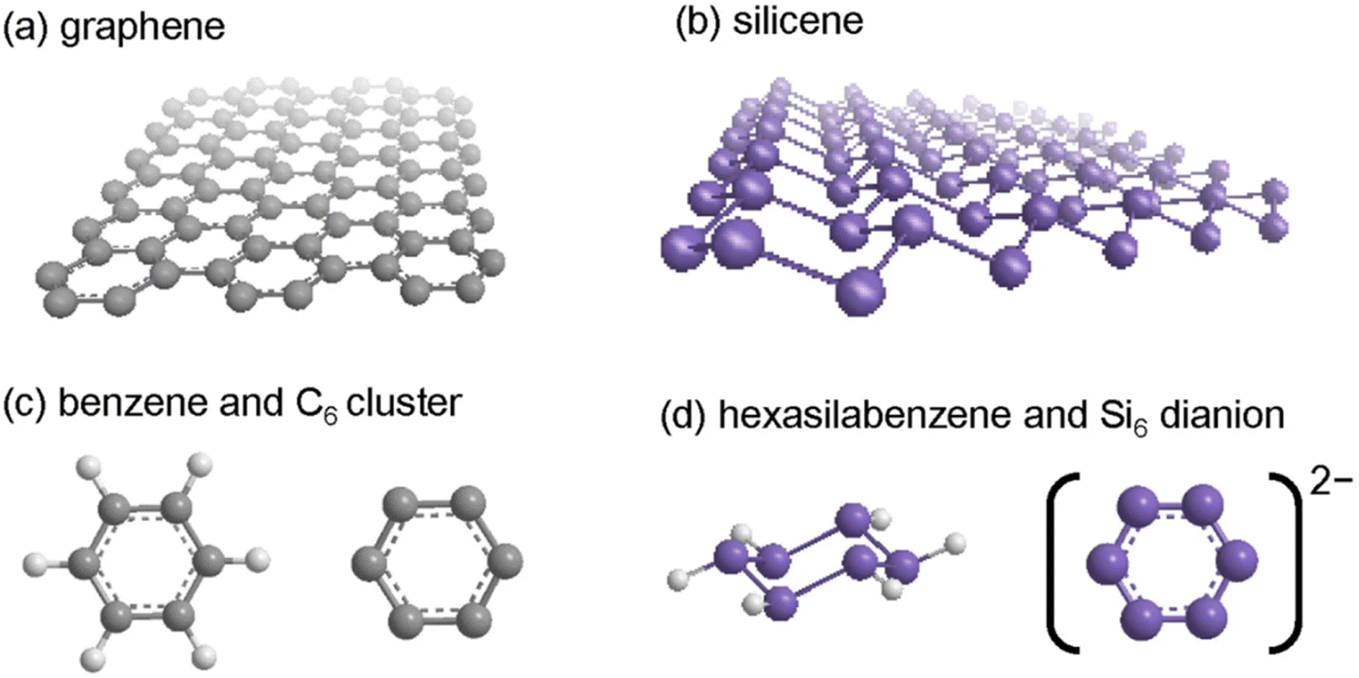 | ||
| Fig. 5 (a) Crystal structure of graphene. (b) Crystal structure of silicene. (c) Structure of benzene and C6 cluster. (d) Structure of silicene and Si6 cluster. Reproduced from ref. 59, copyright 2017. | ||
In 2007, Guzmán-Verri and Lew Yan Voon performed a tight binding Hamiltonian that considers the electronic properties of Si nanotubes. This result showed that silicene is semi-metallic.63 Due to its buckling structure, the thermal conductivity of silicene is much lower than that of graphene. As a result, silicene shows great potential for application in thermoelectric devices.64 Although silicene processes massless Dirac fermions similar to graphene, it is considered that silicene has all the electrical properties of graphene has but with a greater spin–orbital coupling and potential to utilize the quantum Hall spin effect.65 In its basic form, silicene is a conductor due to its zero-band gap.66 Thus, it is very promising for application as a low-energy material. With recent advances in research, silicene has been used for topology-based electronics, such as topological insulator field-effect transistors (TI-FETs). Also, there is increasing research interest in silicene-based junctions or heterostructures, which show great promise for exotic electronic magnetic and thermal applications.67 Silicene shows a lower D3h symmetry, unlike graphene, which shows D6h symmetry.61 However, silicene has better controllability of its band gaps due to its buckled shape.68,69 The band gap of silicene can be opened by chemical functionalization, such as hydrogenation and oxidation. DFT calculation of silicene without spin–orbit coupling always leads to a zero band-gap semiconductor, while spin–orbit interaction opens a fundamental band gap of the magnitude of about 1.55 meV at its Dirac points. Also, without an Ag (111) substrate, silicene opens a 0.3 eV band gap due to structural modification and symmetry breaking by an Ag substrate.62 The formation of vacancies, adatom impurities, and topological defects in the crystal fabrication process is inevitable, which also helps in tuning the band gap of the material. Fig. 6 shows the tuning of the band gap of silicene using oxygen adatoms.70 Due to the buckled structure of silicene, the formation of Stone–Wales defect is more probable than in graphene. The presence of this defect has a crucial effect on the structural, electronic, and chemical properties of silicene.71
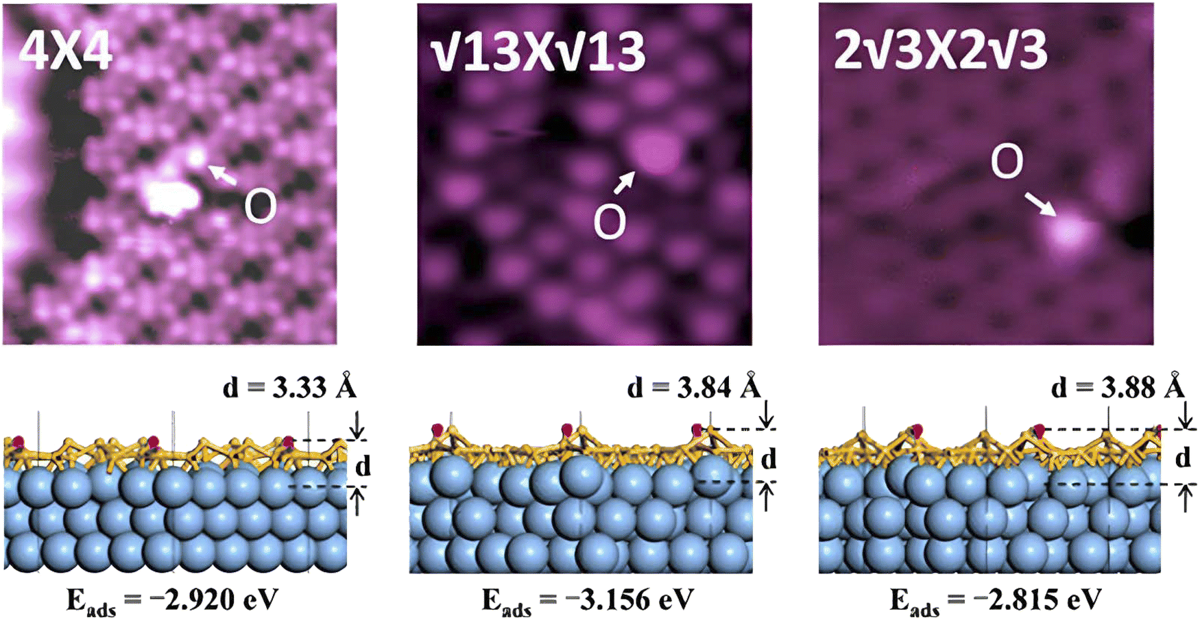 | ||
| Fig. 6 STEM images of silicene modified by oxygen adatoms due to oxidation and corresponding change in its band gap. Reproduced from ref. 70, copyright 2014. | ||
2.8 Germanene
The impressive rise of graphene has made many scientists look for other alternative 2D materials. One of these alternative materials is germanene. In contrast with planar graphene, the honeycomb lattice of germanene is buckled and composed of two vertically displaced sub-lattices.72 The first study on the synthesis of germanene was reported in 2014. In July 2014, Li et al. reported the growth of germanene on Pt (111). Under ultra-high vacuum conditions, a germanium rod was mounted in an electron beam evaporator, from which germanium was deposited on a pristine Pt (111) substrate at room temperature. After deposition, the Pt substrate was annealed at a temperature in the range of ∼600–700 K for 30 min.73 Germanene has the same properties as silicene and graphene, i.e., “zero band-gap.” This band gap can be opened easily if the charge is transferred from one sub-lattice to another sub-lattice, which is also possible because of its buckled shape. Germanium has a larger atomic number compared to carbon. As a result, Ge has a much stronger spin–orbit coupling. Buckling will also increase the spin–orbit coupling by an order of magnitude. This spin–orbit coupling results in the opening of a small band gap at the Dirac points. In germanene, this coupling opens the band gap to about 23.9 meV. In the case of silicene, it is predicted that band gap openings can be realized via the adsorption of alkali atoms on one side of the silicene sheet. Similarly, a sizeable band gap in germanene can be realized by the adsorption of alkali metal.74 Its band gap can be turned from 0.02 eV to 0.31 eV by varying the coverage of absorbed alkali metal atoms.74 Germanene has four possible structural defects, as follows: (1) Stone–Wales defect, (2) divacancy, and (3) pentagonpentagon–heptagonheptagon linear defect. The pentagon–heptagon linear defect has the lowest formation energy, which means that this defect is the easiest to form and the most stable in germanene. In the Stone–Wales defect, 2 heptagons and 2 pentagons are formed by breaking two neighbouring hexagons.75 Germanene has D3d symmetry.72 Similar to graphene and silicene, a germanium monolayer, i.e., germanene, is also a Dirac semimetal.76 The lattice structure of germanene is a buckled honeycomb shape, in which the buckling degree is 0.7, and the bond length is 2.44 Å.77Fig. 7 shows a comparison of the structure and change in the buckling angle of graphene, silicene, and germanene. It was observed that on going down the group, there is a gradual increase in the buckling angle. The interatomic bond is not strong enough to hold the hexagon structure in a planar state.78 Beyond silicene, there has been also work determining the functionalities of other 2D materials.79 Recently, functionalized germanene such as germanane (GeH) has been mass-produced through the topochemical deintercalation of CaGe2. Also, functionalized germanene can be more stable than freestanding germanene due to its lattice distortion. Recently, several procedures have been reported on the chemical functionalization of germanene, for example, foreign element doping (Ti, V, and Cr), hydrogenation, and fluorination. Also, functionalized germanene can present amazing physical and topological properties related to magnetic properties, metallic ferromagnetism, and highly anisotropic optical response.77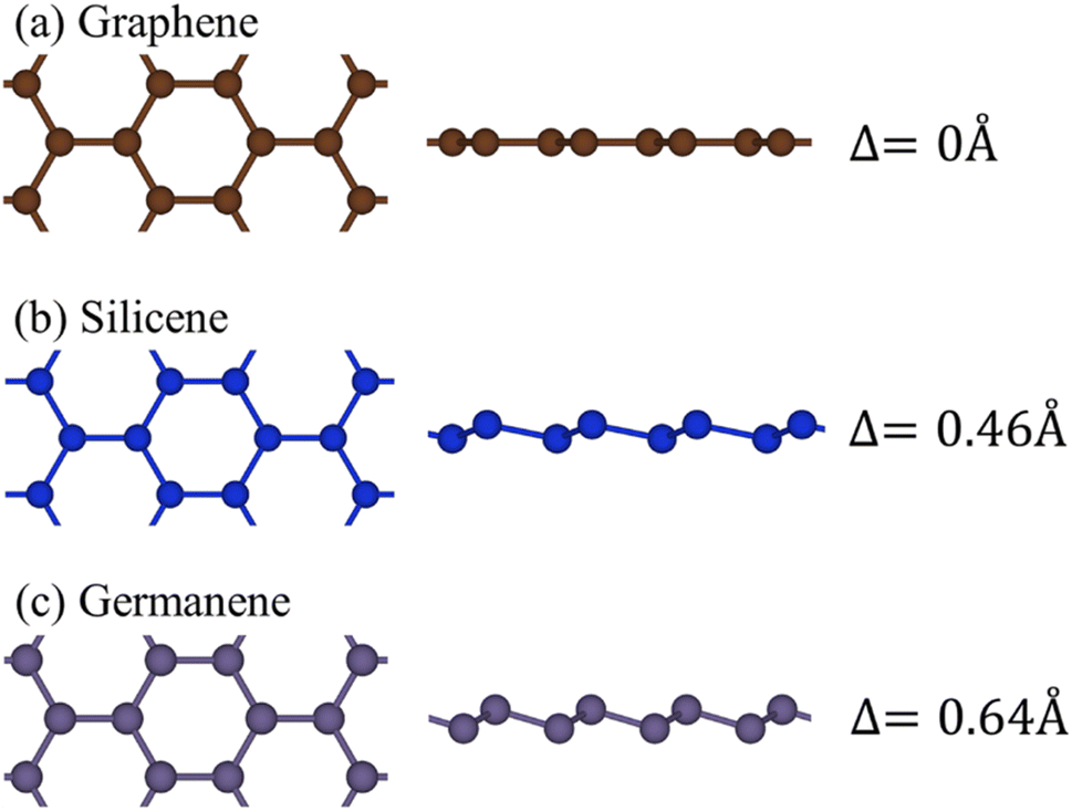 | ||
| Fig. 7 Comparison of the structure and buckling angle among (a) graphene, (b) silicene, and (c) germanene. Reproduced from ref. 78, copyright 2022. | ||
2.9 Stanene
Stanene is known as the latest cousin of graphene, which is similar to 2D graphene materials. However, stanene has an advantage that graphene does not; at room temperature, electrons should be able to travel along the edge of the honeycomb lattice of tin (Sn) without colliding with each other, and thus stanene can be categorized in the subset of topological insulators.80 Generally, 2D materials formed by group IV element (C, Si, Ge, and Sn) atomic arrangements possess a graphene-like honeycomb structure, but stanene has a buckled hexagonal lattice crystal structure. The difference between graphene and stanene is that graphene has a planar hexagonal lattice due to its sp2-type hybridization, whereas stanene has a mixed sp2-sp3 hybridization. Stanene exists in two structural forms, i.e., low buckled stanene (with a lattice parameter of 4.67 Å and buckling parameter of 0.85 Å) and dumbbell unit (with a lattice parameter of 9.05 Å and buckling parameter of 3.41 Å).81Fig. 8 shows the STM image and LEED pattern of as-prepared stanene.82 To determine the mechanical properties of stanene, several uniaxial and biaxial loadings were done along the armchair and zig-zag structure.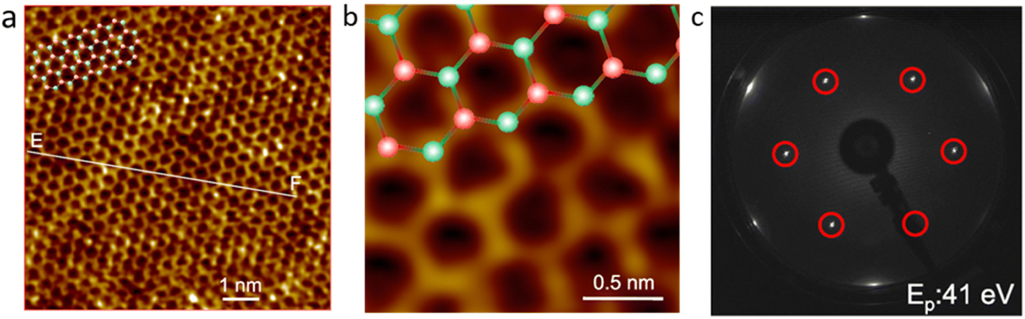 | ||
| Fig. 8 (a and b) High-resolution STM images of stanene. (c) LEED pattern of stanene prepared directly on Ag (111) at 41 eV incident electron energy. Reproduced from ref. 82, copyright 2018. | ||
According to a study, it was revealed that the anisotropic nature of the stability of stanene causes its Young's modulus (E), UTS, and Poisson's ratio (ν) to have different values in different edge directions. The Young's modulus of stanene has been calculated to be approximately 26.684 N m−1.83 In defective stanene, three types of defects are present, i.e., single vacancy, double vacancy, and Stone–Wales defect. The stress–strain response showed that in the case of defective stanene, its tensile strength and elastic modulus decrease with an increase in defect density. Among the defects, the point defect (single vacancy) contributes the least to the decrease in tensile strength and elastic modulus.84 In 2015, the first 2D stanene nanosheet was grown on a metallic Be2Te3 (111) substrate by the molecular beam epitaxy (MBE) process. It was presented that there is no topological state due to high compressive strain; it was buckled, and the growth fashion of tin on the surface of the metal was similar to islands.85 The thermal properties of 2D materials depend on their electron and phonon transport mechanisms. The massless Dirac fermions in stanene follow the modified Wiedemann–Franz (WF) law of electron thermal conductivity (Ke) similar to graphene in the absence of the SOC effect. The electron thermal conductivity (Ke) of stanene is much higher than its phonon thermal conductivity (Kph), which is different to that in planar graphene, and the Ke of stanene also increases with an increase in temperature due to its high energy electrons.83 Stanene has a low buckled honeycomb structure, where its buckled nanostructure weakens the π–π bonding in the Sn atoms and improves the overlapping between σ–π bonding. According to a computational study, it was seen that stanene has a zero band gap excluding spin–orbit coupling, while considering its spin–orbit coupling, its band gap is nearly equal to 0.1 eV.86Fig. 9 represents a recent work where stanene and germanene were combined to form a bilayer. Considering its properties, this bilayer is expected to have potential applications in the solar, energy, and optoelectronic fields.87
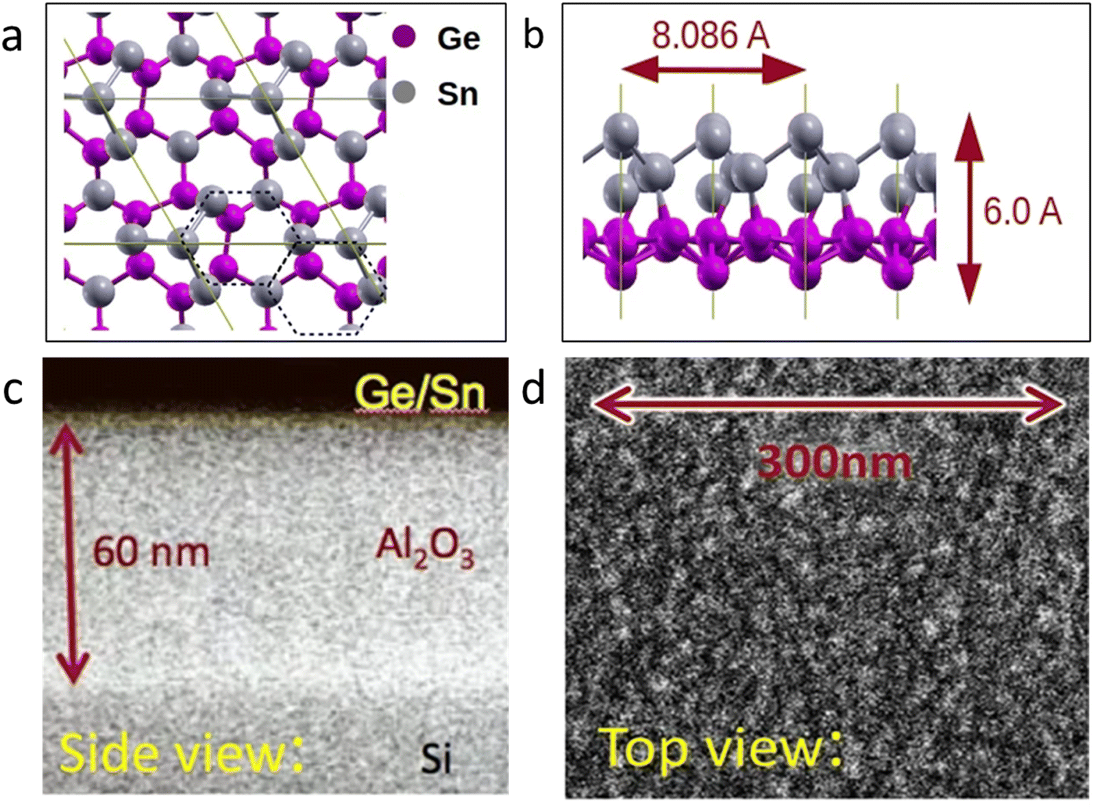 | ||
| Fig. 9 (a) Top view of the germanene–stanene bilayer. (b) Side view of the germanene–stanene bilayer. (c) and (d) SEM pictures of GeSn bilayer placed on a 60 nm-thick layer of Al2O3 from the side and top, respectively. Reproduced from ref. 87, copyright 2023. | ||
2.10 Plumbene
The realization of the last cousin in the group 14 elements, i.e., plumbene, remains a challenging quest, although many theoretical studies predicted its stability and anticipated its outstanding exotic properties. Typically, recently, molecular dynamics simulations revealed that the mechanical properties of plumbene are several times greater than that of bulk lead.88 In April 2019, J. Yuhara and co-researchers reported the large-area epitaxial growth of plumbene by segregation from prepared Pd1−xPbx(111) alloys grown on a Pd(111) substrate upon heating Pb thin films deposited at room temperature. They confirmed the formation of plumbene on these Pd1−xPbx(111) thin films using low-energy electron diffraction (LEED) and scanning tunnelling microscopy (STM).88 As a heavy analogue of graphene, plumbene is a two-dimensional material with strong spin–orbit coupling effects. Using scanning tunnelling microscopy, we observed that Pb forms a flat honeycomb lattice on an Fe monolayer on Ir (111).89 According to Xiang Long Yu and colleagues, plumbene is a topological insulator with a maximum band gap of 0.2 eV upon electron doping. Recent reports suggest that transition metal-doped plumbene exhibits magnetic properties.90 Plumbene has very high bulk band gaps, which are in the range of 1.0911 eV to 1.1515 eV.912.11 Phosphorene
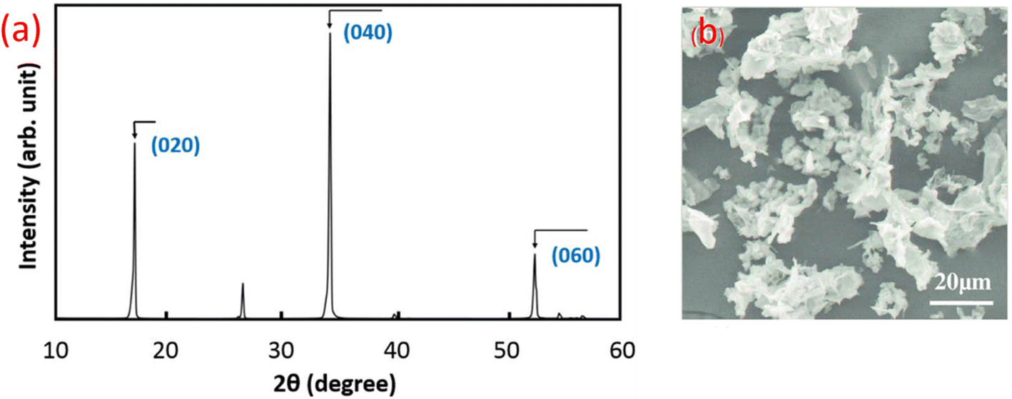
Phosphorous, which is located in group VA of the third period in the periodic table, has different morphologies. Among the different types of phosphorous, black phosphorous is chemically stable and shows the advantage of conductivity compared to red and white phosphorous. The 2D layered semi-conductor material obtained from black phosphorous is phosphorene, which is expected to play an important role in research and many more next-generation application.92–94 Phosphorene has an orthorhombic crystal structure and it shows different mechanical properties. At different pressures, it shows a crystal structure transition. Also, it shows unique mechanical properties for nanoelectrochemical systems and devices. The negative Poisson's ratio of phosphorene gives it a unique puckered structure. Besides, its Young's modulus, composite strength, and tensile strength make phosphorene an efficient filler to reinforce polymers and composites.95American physicist Bridgman won the Nobel Prize in Physics in 1946 for successfully synthesizing bulk BP for the first time by heating white phosphorous to a high temperature of 200 °C under a pressure of 1.2 GPa. The high-pressure synthesis of BP single crystals with a maximum size of 4 mm in diameter and 5 mm in length was first reported by Sugai et al.96 This was performed by the treatment of red phosphorous at 270 °C and 3.8 GPa in a reaction vessel composed of pyrophyllite and equipped with a graphite heater and Pt–Pt 13% Rh thermocouples. Ball milling was also used to convert red phosphorous into BP using steel balls in hardened steel milling vessels, in which a temperature of above 200 °C and high pressure of about 6 GPa were locally generated.97 Black phosphorous crystals show a characteristic X-ray diffractogram, as shown in Fig. 10, with peaks located at (020), (040), and (060) planes, which indicate their crystallinity.
 | ||
| Fig. 10 (a) Powder X-ray diffraction pattern of black phosphorous. Reproduced from ref. 98, copyright 2016. (b) SEM image of porous phosphorous layers. Reproduced from ref. 99, copyright 2019. | ||
Black phosphorous contains some puckered layers that are parallel to the (010) plane of its orthorhombic crystal structure. No peak was observed at 32 °C for the (107) plane of Sn4P3, which indicates the negligible presence of secondary phosphide traces.98 TEM and high-resolution TEM are convenient techniques for evaluating the crystallinity and thickness of phosphorene samples (Fig. 10b). For the measurement of phosphorene flakes, if the thickness of one of the flakes is known, then the thickness of the other flakes can be determined from the contrast using an elastic scattering model. The TEM contrast changes across the flake edge can also be used to distinguish the number of layers, which was four. Fig. 11 shows the HRTEM image and schematic crystal structure of phosphorene.100
 | ||
| Fig. 11 (a) HRTEM image of phosphorene. (b) Crystal structure of phosphorene. Reproduced from ref. 100, copyright 2015. | ||
Phosphorene is an ambipolar semiconductor that shows a band gap between 0.3 eV and 2.0 eV, which depends on its interlayer stacking pattern. This band gap value is slightly higher than that of graphene and similar or smaller than that of MoS2 and WSe2 (1.2–1.8 eV). Defects are inevitably present in materials and always affect their properties. Here, first-principle calculations were performed to investigate the stability and electronic structures of 10 types of point defects in 2d semiconducting phosphorene, including Stone–Wales (SW-1 and SW-2) defect and single (SV-(5|9) and SV-(55|66)) and double (DV-(555|777)-1, (DV-555|777)-2 DV-(555|777)-3, and DV-(4|10|4)) vacancy defects. These defects are all easily created in phosphorene with higher areal density than graphene and silicene. The SW, DV-(5|8|5)-1, DV-(555|777), and DV-(4|10|4) defects have little effect on the electronic properties of phosphorene, and defective phosphorene monolayers are still semiconducting with similar band gap values to perfect phosphorene.101
2.12 Arsenene
2D arsenene and arsenic, as members of the 2D Group-VA materials, have attracted increasing interest over the past few years. The diverse crystalline phases, exotic electrical characteristics, and widespread application of 2D arsenene and arsenic endow them with great research value and utilization potential. Moreover, 2D arsenene and arsenic have potential in a wide range of the applications including field effect transistors, sensors, catalysts, and biological applications.102 Arsenene has been found to possess a honeycomb crystal structure, together with superior mechanical properties, high carrier mobility, and negative Poisson's ratio. The mechanical properties of arsenic heterostructures include stiffness and hardness. The Young's modulus of all arsenene heterostructures is in the range of 600–800 GPa, which is much higher than that of the main inorganic components in the natural solid electrolyte interphase. In the study by Shang et al., an arsenene/graphene heterostructure was found to possess extremely high mechanical strength, which can effectively inhibit the puncture of lithium dendrites and improve the performance of lithium batteries.103The preparation and realization of 2d arsenene and arsenic have been carried out successfully in recent years. The methods employed include epitaxial growth, mechanical exfoliation, and liquid phase exfoliation, which have advantages and disadvantages. Besides the top-down methods, bottom-up strategies are also effective and crucial in preparing high-quality 2D materials for the large-scale production of particle devices. Selecting the appropriate precursor and substrate is vital to the growth of 2d arsenene and arsenic materials on certain substrates. Monolayer grey arsenene was successfully grown on an Ag (111) substrate via MBE (molecular beam epitaxy) by heating it as a crystal to generate a precursor species. The crystallization temperature mostly determined the synthesized crystal phase of arsenene. A crystallization temperature of arsenic above 360 °C, less than 300 °C, or rapid cooling will lead to the formation of grey arsenic, amorphous arsenic, and yellow arsenic, respectively.102 The electronic structure of buckled arsenene with a buckling parameter (1.39 Å) corresponds to that of a semiconductor with an indirect/direct bandgap of 1.63/1.97 eV. Defects, especially point defects, can dramatically affect the electronic, magnetic, thermodynamic, and optical properties of 2D arsenene-based devices. In the fabrication and processing of 2D materials, point defects are inevitable, and the most typical point defects found in other 2D materials are Stone–Wales defects, single vacancy, double vacancy, and adatoms. These defects were systematically studied using density functional theory (DFT) and Car–Parrinello molecular dynamics (CPMD). Thus, it is very important to understand the effects of these defects on arsenene, which will help create ideas to control defects to prepare new arsenene-based materials with novel properties.104Fig. 12 presents the partial oxidation of arsenene. It was discovered that oxidation may reduce the direct bandgap of oxidized arsenene from 1.29 to 0.02 eV by increasing the oxygen concentration from 1O/18As to 18O/18As.105
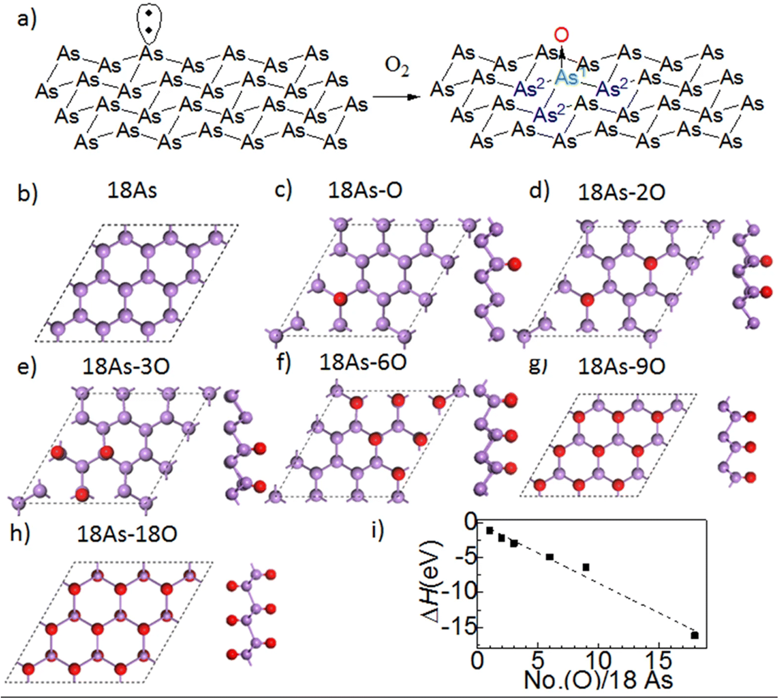 | ||
| Fig. 12 (a) Partial oxidation of arsenene. (b–h) Partial oxidation of arsenene in different ratios. (i) Change in enthalpy with respect to the degree of oxidation of arsenene. Reproduced from ref. 105, copyright 2016. | ||
The phase purity of the materials was identified by X-ray diffraction, confirming the rhombohedral and orthorhombic structures for grey and black arsenic, respectively, as shown in Fig. 13. Firstly, the rhombohedral crystal structure of grey arsenic was confirmed with the most intense diffraction pattern at 2θ = 32.2°, corresponding to the (012) reflection. Some minor peaks have arisen due to the presence of AS2O3. The XRD pattern of the exfoliated black arsenic was confirmed with a sharp doublet peak at the 2θ values of 32.55° and 32.80°, corresponding to the (004) and (111) phases, respectively. The presence of arsenic oxide is much more pronounced in the black AS, and there were also some minor peaks arising due to rhombohedral arsenic.106
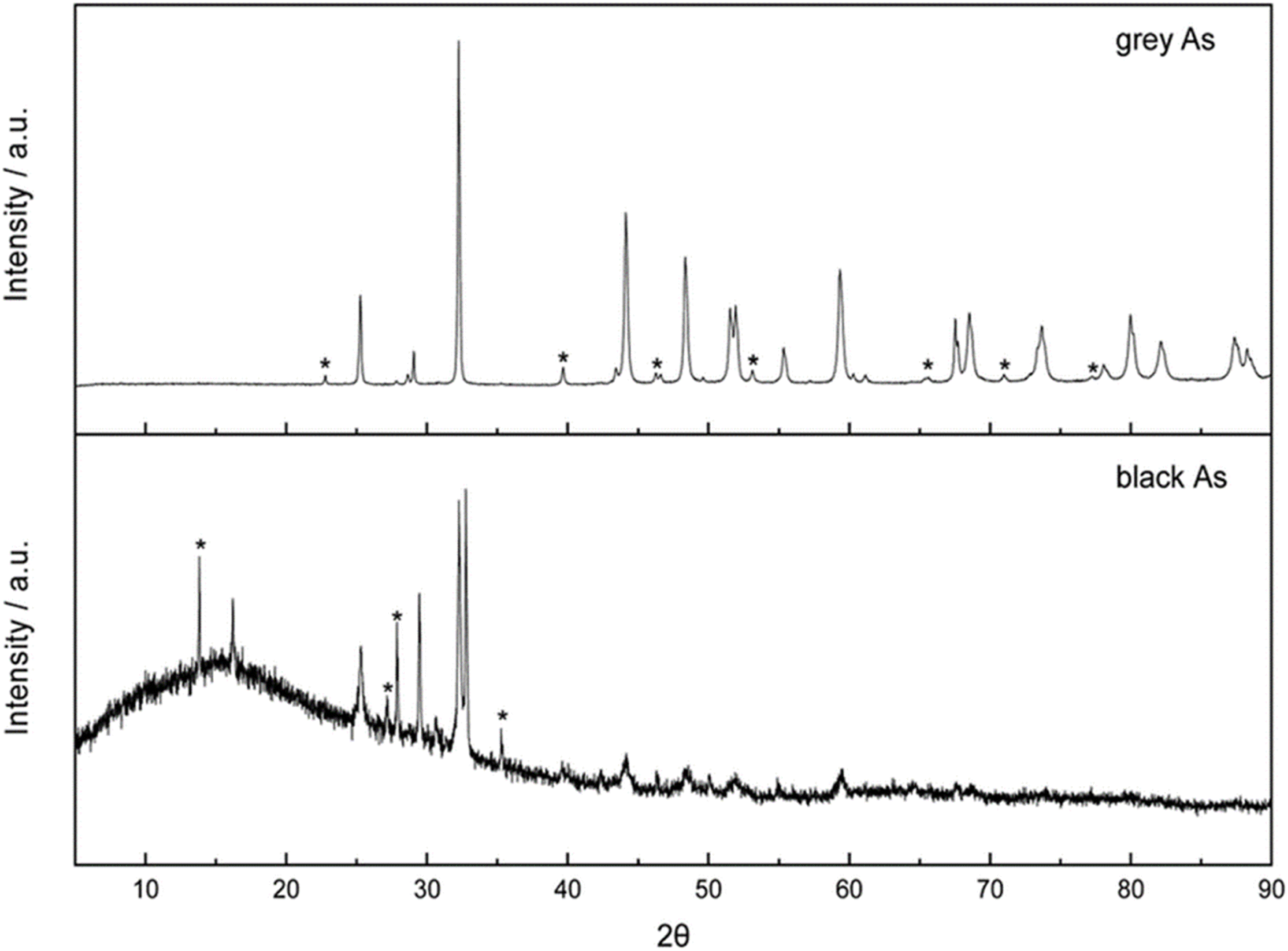 | ||
| Fig. 13 Powder X-ray diffraction patterns of grey arsenic thin layer (above) and black arsenic thin layer (below). The star-marked peaks represent arsenic oxide impurities. Reproduced from ref. 106, copyright 2020. | ||
2.13 Antimonene
Among the 2D materials, antimonene has gained popularity since 2016.107 Also, we should point out that the name antimonene is not completely correct given that there is no double bond in its structure.108 However, it remains challenging to prepare high-quality antimonene due to its strong bonding energy and ultrashort layer distance. Recently, Periñán et al. developed mechanical and liquid-phase exfoliation methods for the preparation of antimonene. Gibaja et al.109 reported the use of liquid phase exfoliation for the first time to prepare few-layer antimonene. The best solvent obtained was a 2-propanol–water (4![[thin space (1/6-em)]](https://www.rsc.org/images/entities/char_2009.gif) :1) mixture. The LPE process requires 30 h of sonication to prepare antimonene, which is very consuming. Thus, a modified method to that for antimonene, including ball-milling for 180 min at 3000 rpm followed by sonication for 40 min, was developed to produce a more homogeneously sized material. The yield was also enhanced with a concentration of 0.014 g L−1 compared to that of 1.74 × 10⁻³ g L−1 previously reported.18 Antimonene has a buckled honeycomb structure with the Rm space group, unlike graphene, which has a planar structure. The lattice constant of antimonene was determined to be 4.12 Å, while its Sb–Sb bond length and angle were found to be 2.95 Å and 88 Å, respectively. Also, the structure of its unit cell is rhombohedral.108,110 The band gap of single-layer antimonene is about 1.2 eV.108 Bilayer antimonene is an indirect band gap semiconductor with a band gap of 0.36 eV for AA stacking and 0.25 eV for AB stacking.111 Also, antimonene has a tunable band gap in the range of 0–0.28 eV.112 Defects are inevitably present in materials. Thus, similar to other 2D materials (silicene, germanene, and graphene), antimonene possesses vacancies and Stone–Wales defects.113
:1) mixture. The LPE process requires 30 h of sonication to prepare antimonene, which is very consuming. Thus, a modified method to that for antimonene, including ball-milling for 180 min at 3000 rpm followed by sonication for 40 min, was developed to produce a more homogeneously sized material. The yield was also enhanced with a concentration of 0.014 g L−1 compared to that of 1.74 × 10⁻³ g L−1 previously reported.18 Antimonene has a buckled honeycomb structure with the Rm space group, unlike graphene, which has a planar structure. The lattice constant of antimonene was determined to be 4.12 Å, while its Sb–Sb bond length and angle were found to be 2.95 Å and 88 Å, respectively. Also, the structure of its unit cell is rhombohedral.108,110 The band gap of single-layer antimonene is about 1.2 eV.108 Bilayer antimonene is an indirect band gap semiconductor with a band gap of 0.36 eV for AA stacking and 0.25 eV for AB stacking.111 Also, antimonene has a tunable band gap in the range of 0–0.28 eV.112 Defects are inevitably present in materials. Thus, similar to other 2D materials (silicene, germanene, and graphene), antimonene possesses vacancies and Stone–Wales defects.113
2.14 Bismuthene
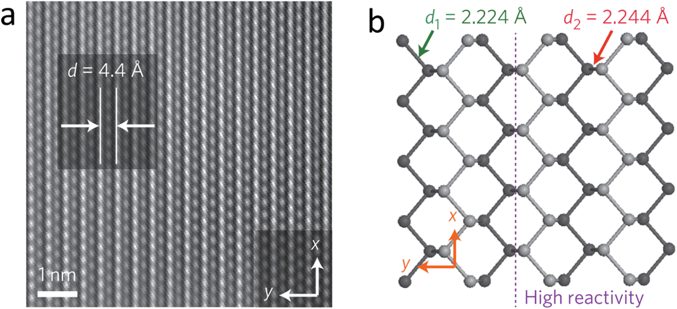
Among the group 15 elements (pnictogen family), the heaviest element is the bismuth, which forms a monolayer nanomaterial called bismuthene. The explosive growth of this new 2D nanomaterial is due to its tunable electronic, optical, catalytic, and electromagnetic properties.16 Bismuthene has a 2D hexagonal lattice and honeycomb structure with optimized lattice constants of a = b = 4.38 Å. Its Bi–Bi bond length is d1 = 3.07 Å. Three alternating atoms at the corner are raised, and the remaining three are lowered. Bismuthene has two atomic planes, where the distance between two planes or buckled angles is 1.74 Å. The 2D structure of bismuthene is stabilized by buckling, where its planar sp2 bond is rehybridized to sp3 hybridization to compensate for the relatively weaker pi–pi bonding that generally favors planar 2D graphene.114 Bismuthene films were produced using the sonochemical exfoliation method, where first-bump bismuthene was ground with isopropyl alcohol. Then, 0.5225 mL of bismuthene isopropyl alcohol solution and 9.4775 mL of isopropyl alcohol were placed in a spiral bottle glass and kept in ice bath sonication and a probe sonication machine at 5000 rpm for 20 min.115 According to the TEM images, the synthesized few-layer bismuthene showed a lateral size of approximately 0.8 μm. Using high-resolution transmission electron microscopy, it was observed that bismuthene has a rigid arrangement lattice plane. The interlayer spacing of its lattice planes is 0.322 nm, which is in accordance with the (111) interplanar distance of the rhombohedral A7 structure. According to SEM, it was confirmed that bismuthene has a crystalline structure. The SEM and TEM images of the prepared bismuthene are presented in Fig. 14.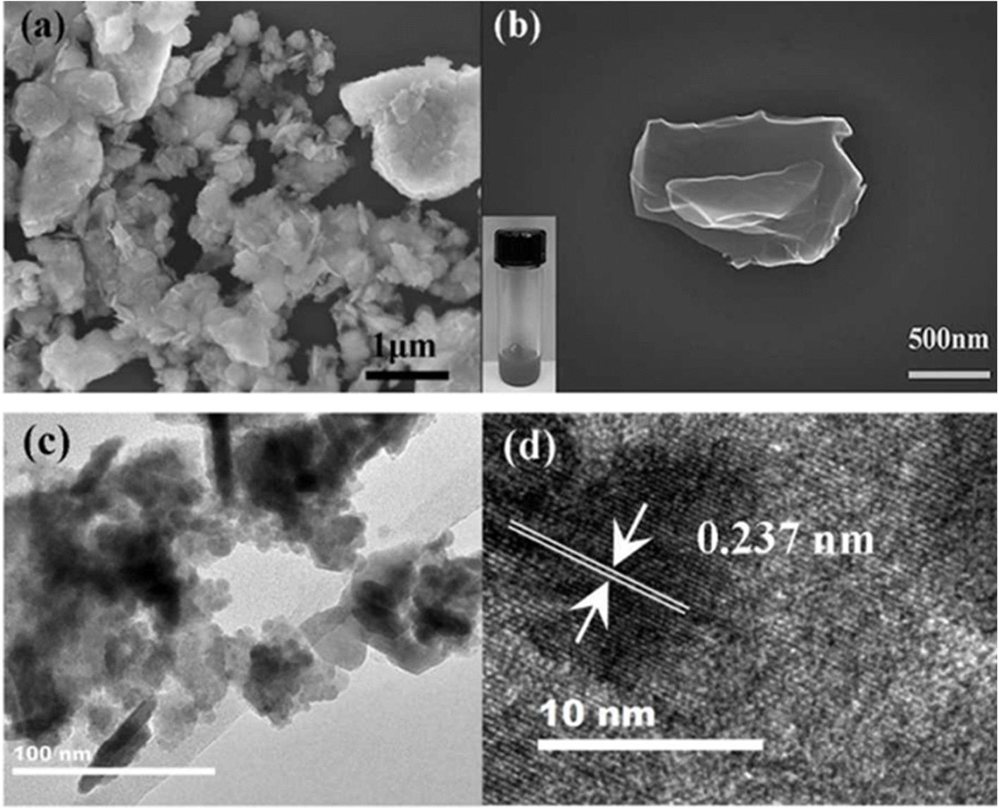 | ||
| Fig. 14 (a and b) SEM image (c) TEM images (d) HRTEM image of the synthesized bismuthene. Reproduced from ref. 116, copyright 2018. | ||
As shown in Fig. 15A, AFM images confirm that nanoflakes have a height of 4 nm with a smooth surface. According to the high-resolution X-ray diffraction (HRXRD) of bismuthene powder, it was reported to have a space group of R![[3 with combining macron]](https://www.rsc.org/images/entities/char_0033_0304.gif) m. The X-ray photoelectron spectrum (XPS) of bismuthene showed three sharp photoelectric peaks at 23.6 eV, 25.9 eV, and 28.8 eV, corresponding to the Bi–Bi 5d(5/2), 5d, and 5d(3/2) orbital bonding, respectively, as shown in Fig. 15B.115
m. The X-ray photoelectron spectrum (XPS) of bismuthene showed three sharp photoelectric peaks at 23.6 eV, 25.9 eV, and 28.8 eV, corresponding to the Bi–Bi 5d(5/2), 5d, and 5d(3/2) orbital bonding, respectively, as shown in Fig. 15B.115
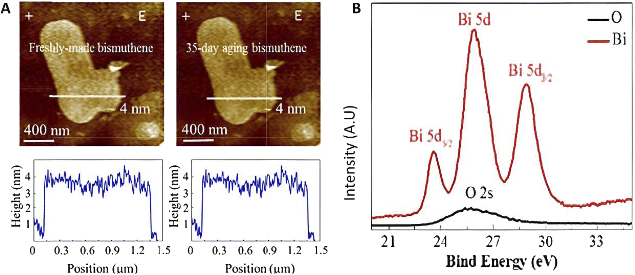 | ||
| Fig. 15 (A) AFM images of few-layer bismuthene before and after 35 day aging and (B) X-ray photoelectron spectrum of bismuthene. Reproduced from ref. 115, copyright 2018. | ||
2.15 Sulfurene
The last group, 16, starts with sulfur, where the thinnest sulfur nanosheets have been synthesized. This Xene material is named sulfurene, which has a thickness of 0.84 nm. In the work by Bai et al., sulfurene was prepared using sublimed sulfur as the raw precursor. Initially, the hydrothermal-assisted method yielded sulfur nanosheets, which on further exfoliation, produced sulfurene.117 It was observed that the aqueous medium reduction of S(0) to S2− occurred at an applied potential of −1.2 V.117 Currently, no other work has been reported on preparing sulfurene-based systems. It is expected that this low-cost material will be a good choice for energy applications, such as sulfur-based batteries.2.16 Selenene
Selenene is a 2D Xene material that is produced from the chalcogen metal selenium. Selenium has a small band gap (1.35 eV) and low-dimensional and anisotropic elemental semiconductor properties. Selenene has a helical chain-based crystal structure and exists in both two-dimensional (2D) forms, such as layered-thin films, and one-dimensional (1D) configurations, such as nanowires. Selenene is a 1D van der Waals material,118 where the Se atoms are generally bonded with their two neighbouring atoms, producing a helical atomic chain that is parallel to the [0001] direction (c-axis). The atomic chain of Se atoms is packed by van der Waals forces to create a hexagonal lattice structure. For the synthesis of selenene, various techniques have been developed, among which, three major techniques are available for the synthesis of selenene nanotubes and nanowires. One is the biomolecule-assisted hydrothermal synthesis by SeO2,119 the second is porous templated-assisted methods in a photodetector system, and the third is physical vapor deposition. Using the physical vapor deposition method (PVD), the prepared selenene was reported to be 10 μm in the lateral direction and 5 nm in thickness. In this process, a multizone furnace was used, where Se powder was placed in one zone, and Si (111) substrate was placed in the other zone. Ar gas was passed through the furnace for 60 min.120 The process was complete with a saw-like structure where one side was a zig-zag edge, resulting in the formation of an Se nanosheet, which was confirmed by TEM, SEM, and AFM images.1202.17 Tellurene
Tellurene is a nanomaterial that is produced from chalcogen metal tellurium (Te), similar to selenene. Te is also a recently developed elemental semiconductor with good piezoelectricity, photoconductivity and thermoelectricity properties. Te has a small band gap (0.35 eV) at room temperature and shows much higher electron mobility than Se. Tellurene possesses a chain-based crystal structure, which exists as two-dimensional and one-dimensional nanowires. 1D tellurene is a van der Waals material in a hexagonal lattice system of a chain of tellurium atoms.121Various methods have been developed for the synthesis of 1D and 2D tellurene nanomaterials. Among them, the generally used methods with good results are physical vapor deposition (PVD),122 pulsed laser deposition, magnetron sputtering,123 liquid phase exfoliation, hydrothermal synthesis, and encapsulation in nanotubes. Here, we only discuss the synthesis of tellurene by physical vapor deposition. In this process, a two-zoned furnace is used, where in one zone, the source material is placed in the hot end at about 650 °C and silicon with 300 nm silicon dioxide (SiO2/Si) substrate is placed at the other cold end. Ar gas with 15% hydrogen is used as the carrier gas, which transfers the source vapor to the substrate. The dimensions of flakes produced are around 10–100 μm.122
2.18 Poloniumene
The last element in group 16 is polonium. In a few recent theoretical studies, the structural properties of 2D mono-elemental polonium systems have been analysed. According to these theoretical studies, it has been found that poloniumene consists of a structure similar to that of MoS2,124 where it is known as trigonal poloniumene. Here, in this material, the central Po is metallic, whereas the other two Po atoms are semiconducting in nature.125 Currently, no experimental work has been reported on the fabrication of this material, where it is obvious that the radioactive nature of this material prevents it.3. Applications
3.1 Catalysis application
One of the most dominant fields of research involving the constant effort of materials in energy research is the catalysis field. Current catalysis research can be mainly classified into electrocatalysis and photocatalysis. As is name suggests, an electrical current is used in the electrocatalytic process. Alternatively, in photocatalysis, a photocatalyst harvests and uses light energy in a photochemical process. In the literature, there are several instances where graphene was used as a catalyst material,126–129 which is attributed to the wide possibility of engineering graphene.130 These different possibilities can be facilitated by various point defects such as substitution,131 adatoms,132 vacancies,133 and Stone–Wales defects.134 The line defects include dislocations135 and grain boundaries.136 Lastly, the interlayer defects include stacking faults137 and interlayer interstitials.130 It also must be considered that graphene can be employed for the synthesis of composite materials as catalysts. A study has reported that any doping in graphene can influence its electrical properties. As a result, there are 84 stable elements that can be used as a mono-elemental dopant, 3486 bi-elemental dopants, and around 2 × 10⁶ combinations of tri-elemental dopants for graphene.138Obviously, there are several factors to consider, such as that not all dopants are cost-effective. Also, an increase in the complexity of the synthesis technique will add to the question of the practicability of the new material. As a result, new materials, as discussed in the introduction, are emerging. These new materials, in various aspects, have surpassed graphene and its derivatives. One new possibility is the advent of these materials in the catalysis field. Not all these materials have been used to date in the application of catalysis. However, considering their graphene-like nature, such as high surface area, semiconducting to metallic properties, and high functionalization capabilities, it can be stated that they will be good electro/photocatalysts. When describing the current research in the field of electro/photocatalysis, the most widely desired current research processes include HER (hydrogen evolution reaction),139 OER (oxygen evolution reaction),140 NRR (nitrogen reduction reaction),141,142 and CO2RR (carbon dioxide reduction reaction).143 These processes can take place either by the photochemical or electrochemical pathway, depending on the catalysis process.
Now, regarding the question of selecting Xenes instead of graphene. One may wonder what are the reasons for choosing Xene systems instead of the widely available graphene and other 2D materials. One reason is that some limitations can be overcome by using Xene materials. For example, in the case of graphite, the commonly used anode material, it has a low theoretical capacity of 372 mA h g−1, whereas phosphorene, as an alternative to graphite, has a theoretical capacitance of 2596 mA h g−1.144 Regarding catalysis, materials such as borophene phosphorene can be passivated by the use of hydrogen, resulting in faster free carrier transport.144 In recent works, it has been found that silicene has hydrophilic properties as a result of autocatalysis of its hydrogen atoms. It has been predicted that this autocatalysis property of silicene can have wide application in metal-free catalysis for ORR and water-splitting processes.145 Besides, there is also the possibility of defect engineering, similar to graphene, which opens the chances of the use of Xenes in catalytic applications.144 For example, Co atoms on phosphorene have been found to improve its OER activity. Also, Co co-modified phosphorene has been found to show remarkable stability compared to that of the commercial electrocatalyst IrO2.146
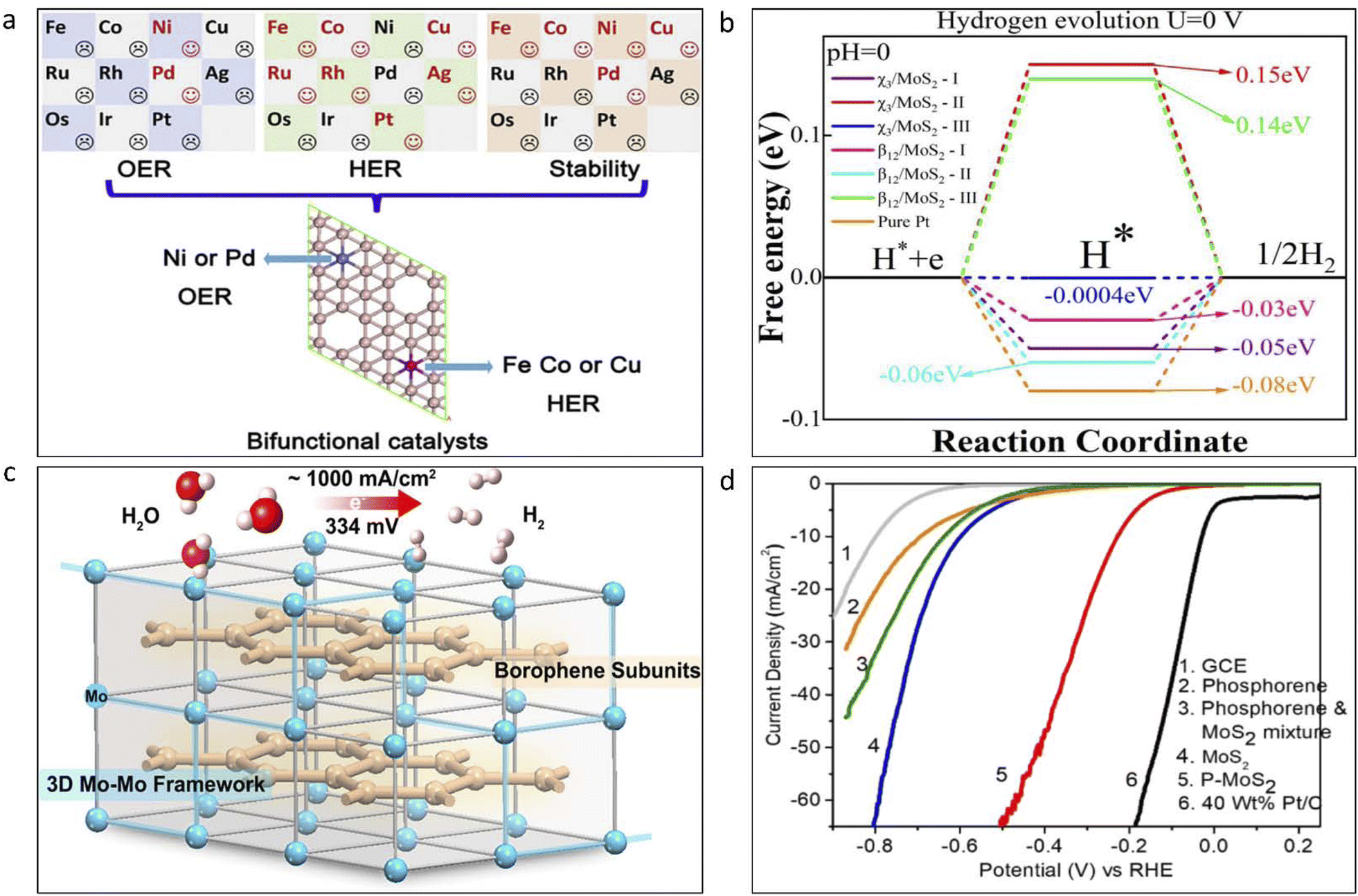 | ||
| Fig. 16 (a) Effect of doping of different transition metals on the bifunctional HER and OER activity of borophene. Reproduced from ref. 154, copyright 2020. (b) Plot showing the variation in Gibbs free energy (ΔGH*) for hydrogen (H) adsorption. Reproduced from ref. 160, copyright 2024. (c) Borophene subunits consisting of non-precious electrocatalysts such as Mo for use in hydrogen evolution. Reproduced from ref. 161, copyright 2017. (d) LSV curves of different materials for use in HER compared to that of Pt electrodes. Reproduced from ref. 162, copyright 2019. | ||
In group 15, phosphorene, arsenene, and antimonene have mainly contributed to the development of HER and OER catalysts.163–165 Based on the band structure of phosphorene, it has been predicted that it can only be used as an HER catalyst. However, in the recent work by Hu et al., they modified the edge sites of phosphorene nanoribbons, which resulted in a significant improvement in solar water splitting.166 Black phosphorene has also been proven to be effective in solar water splitting by working as an OER catalyst.167 Judging from the various works in photocatalysis, it can be said that phosphorene can be upscaled for use as a catalyst for photocatalytic water splitting.166–169 Phosphorene-based 2D materials show pyrocatalytic behavior in hydrogen production. Fig. 17 presents a schematic of the working mechanism of black phosphorene in pyro-catalytic hydrogen production.170
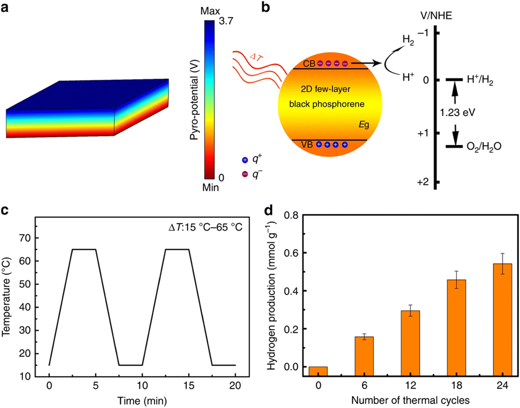 | ||
| Fig. 17 (a) Pyro-potential of 2D phosphorene. (b) Schematic diagram on the effect of hydrogen production by the pyroelectric effect. (c) Temperature curve of cold–hot cycles. (d) Pyro-catalytic hydrogen generation. Reproduced from ref. 170, copyright 2018. | ||
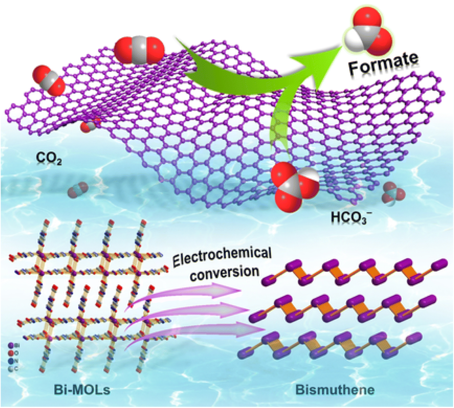 | ||
| Fig. 18 Schematic diagram of electrocatalytic reduction of CO2 to formate using bismuthene. Reproduced from ref. 182, copyright 2020. | ||
3.2. Supercapacitor application
The never-ending pursuit of high-power density energy storage devices to achieve ever-withstanding internal combustion engine/wired electrification is devoted to making use of diverse energy sources.184 Supercapacitors as electrochemical capacitors are well-known for their high-power density delivery through fast charging–discharging process. The world is moving towards a wireless civilization, where electrovoltaic (EV) devices will be the heart of the electrical future. They have the capability to provide energy quickly with stability to run machinery and again recharge rapidly for the next run. In 1746, the Dutch invention of the Leyden jar was the innovative discovery with the strongest base root in the field of energy storage. This induced a new field of energy storage and conversion.185 Subsequently, the electrochemical capacitor (supercapacitor) was explored in 1879 by Helmholtz, who modified the surface chemistry with an electrical double layer at the electrode interface.186 Becker et al. first reported a carbon electrode supercapacitor with similar energy density to a battery and 4–5 times greater power density than ordinary capacitors.187 Since then, the research on supercapacitors has fully accelerated to modify their power density, cycle life, and potential window.Depending on their charge storage mechanism, supercapacitors are classified as electrochemical double-layer capacitors (ELDC), which are directly dependent on the specific area of the active electrode material.188–190 Briefly, a capacitor is an engineering product that can store electric energy in the presence of electric field. The role played by the capacitor is to generate capacitance, which is a physical charge storage process at the interface. Electrochemical energy is stored in an electrochemical double-layer supercapacitor via the physical adsorption of ions from the electrolyte, and some amount of charge is also stored in the electrochemical redox process at the surface of the active electrode material.191–193 In the present studies on 2D materials, they have an inherent huge specific surface area, extraordinary mechanical strength, and flexibility144 to be successfully employed in supercapacitor applications.
In borophene, the boron atoms in a single layer form a honeycomb lattice, facilitating unique electronic properties that are suitable for supercapacitor application. Initially, boron-based advanced materials were designed for mechanotribological applications such as ternary transition metal borides/metal aluminium borides with nano-laminated sheets.194 Later, boron materials were investigated for electronic and electrochemical applications through boron carbide, nitride, boron-doped diamond, etc. Simru et al. designed a composite, i.e., PANI: alpha-borophene, with the corresponding electrodes showing a specific capacitance of 960 F g−1 and capacitance retention of 95%.195 The boron-based electrode showed an average supercapacitive performance in aqueous electrolytes. Further, one modification analogous to graphene oxide, oxygen defects in boron nanosheets, facilitated high-performance pseudocapacitive charge storage in both aqueous and non-aqueous electrolyte media. In Fig. 19, it can be found that the oxygenated boron nanosheets showed the conductivity of 96.12 Sm−1 and fantastic pseudocapacitive contribution (141.55 mF cm−2 at 2 A g−1) in 1 M H2SO4 aqueous medium.24 In most of the works, there have been cases of the use of multilayer borophene given that the synthesis of monolayer borophene is difficult. Here, oxygen defects were generated by the oxidation of borophene sheets, and it was found that they showed a good capacitive performance.24
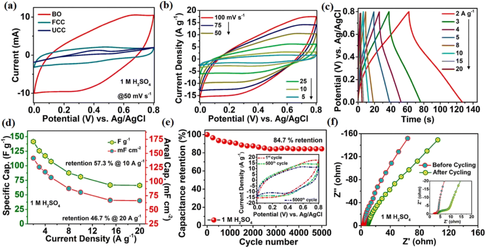 | ||
| Fig. 19 Electrochemical redox property analysis in 1 M H2SO4 aqueous electrolyte. (a) Cyclic voltametric response of oxygenated borophene (BO), functionalized carbon cloth, and unfunctionalized carbon cloth. (b) Cyclic voltametric curve of BO at multiple scan rates. (c) Charge–discharge profiles at different current densities. (d) Specific capacitance and areal capacitance of BO at different current densities. (e) Cycle stability at 100 mV s−1 scan rate for a large number of cycles. (f) Nyquist plot together with the electrochemical impedance spectra before and after large cycling. Reproduced from ref. 24, copyright 2021. | ||
A wide potential window is an attractive choice for power tool applications; it enhances the power density of a supercapacitor with ionic liquid electrolytes, which are stable at a higher voltage.196 A. Joshi et al. reported that oxygenated boron nanosheets (same above-discussed material) can perform electrochemical energy storage at elevated temperature up to 60 °C at a stable 3 V potential window of up to 2.85 V in BMIMBF4 ionic liquid electrolyte, which is definitely larger than that in aqueous system or ambient temperature. They achieved a 5-fold current density increment in non-aqueous media, 25.1 W h kg−1 energy density, and 636.13 W kg−1 power density. As can be seen in Fig. 20, cyclic voltammetry curves show enhanced electrochemical performance at elevated temperatures, i.e., 60 °C. Again, in Fig. 20b, the electrochemical impedance spectrum justifies the improvement at elevated temperatures. This is because of the correlation between viscosity and hindrance; as temperature increases, ionic mobility also increases, which results in high conductivity through fast transportation. In Fig. 21c, the relaxation time constant shows that it can deliver energy nearly five times faster at elevated temperatures. In the galvanostatic charge–discharge profile, up to 78.88 F g−1 capacitance was achieved at 2 A g−1 current density and reduced to 30.78 F g−1 at 10 A g−1 current density (Fig. 20e).
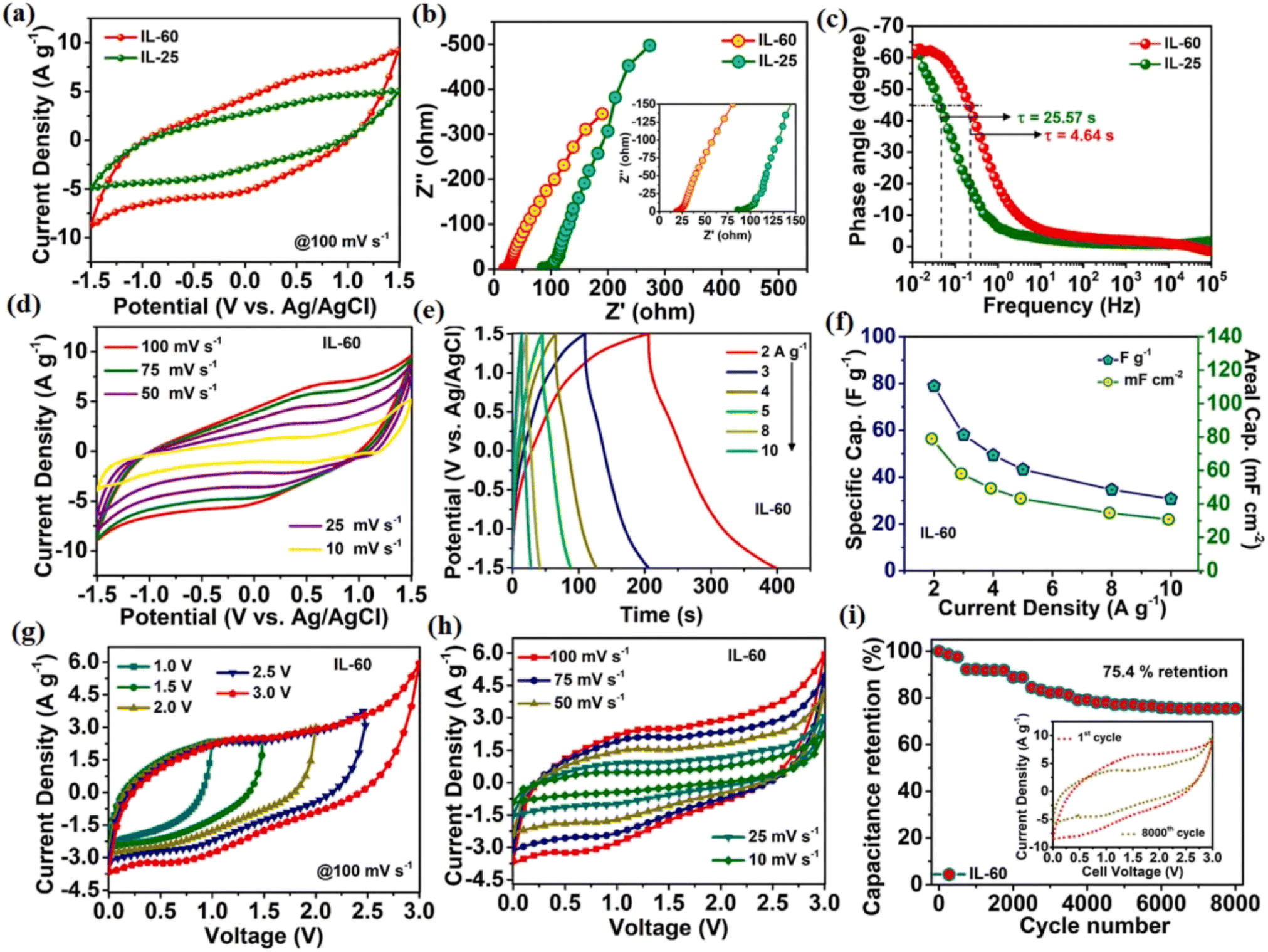 | ||
| Fig. 20 Electrochemical performance of oxygen-defected borophene (BO) electrode in BMIMBF4 ionic liquid (IL) electrolyte. (a) Comparison of voltammetry curve of oxygenated borophene in IL-25 °C and IL-60 °C. (b) Comparison of temperature effect in Nyquist plot of oxygenated borophene in IL at IL at 25 °C and 60 °C. (c) Relaxation time constant determination. (d) Voltametric responses of oxygenated borophene in IL at 60 °C. (e) Charge–discharge profile of BO in IL at 60 °C with respect to different current densities. (f) Rate capability of oxygen-defected borophene in IL at 60 °C. (g) Cyclic voltammetry-based potential window stability study of a symmetric cell. (h) Cyclic voltametric profile of BO symmetric cell as a function of scan rate. (i) Capacity retention study of BO symmetric cell for large cycle number at 300 mV s−1 scan rate. Reproduced from ref. 24, copyright 2021. | ||
 | ||
| Fig. 21 (a) Rate kinetics of silicene-graphite composite electrode (green symbol) and commercial graphite (gray symbol), (b) charge–discharge profile of the electrode, (c) electrode cyclability study, (d) dQ/dV plots from cyclic voltammetry study, and (e) electrochemical impedance spectrum of silicene–graphite composite electrode at various cycle numbers and an equivalent circuit. Reproduced from ref. 63, copyright 2023. | ||
In 2014, after the discovery of 2D black phosphorus, it was found to be analogous to graphene.197 It possesses a band gap of 1.5 eV, which is greater than that of bulk black phosphorous, i.e., 0.3 eV,198 and as the spacing increases between two successive layers, its band gap decreases accordingly.198,199 It has two unoccupied electron pairs on each atom, which make it highly reactive.200 Puckered-structured phosphorous has good conductivity and fast ion diffusivity, which make it suitable for application in supercapacitors. Hao et al. explored a flexible supercapacitor using black phosphorous nanoflakes, which showed a specific capacitance of 59.3 F g−1 at 5 mV s−1 with a great cyclability of 30 k charge–discharge, retaining 71.8% capacitance.201
The justification of the silicene supercapacitor was explored first by computational DFT studies.202 Similar to the battery-like anode, defect-mediated (both vacancy and doping) active sites can enhance the quantum capacitance.203 Phosphorene (2D single/few layers of black phosphorous) has an issue in the ambient environment, given that it is hygroscopic and deteriorates in the open air, limiting its practical applications.204 This led to the search for new 2D sheet-like nano-flake materials for use in the ambient environment. Antimony crystal-derived antimonene flakes were stable for more than 60 days under atmospheric conditions.205 They exhibited a theoretical capacity of 660 mA h g−1 for both Li and Na ions.206 In a realistic approach, Hou et al. explored a 2D antimony–carbon fibre networked anode for a sodium-ion battery, showing an electrode capacity of 542 mA h g−1 at 100 mA g−1 with good cyclability of 96% after 100 cycles.207 Arsenene has an indirect band gap of 1.5–1.7 eV, giving a new opportunity to enter the modern world. Transition metal-doped arsenene is theoretically found to be a good asymmetric supercapacitor application. First principles studies revealed that 3d/4p doping in arsenene enhances its quantum capacitance; among them, chromium-arsenene and selenium arsenene have an impactable value of 345 microfarad cm−2 and 176 microfarad cm−2 in positive and negative bias, respectively.208
3.3. Battery application
Batteries have been developed with a higher energy density and much longer discharge time for long-term application. The materials that can hold electrical charges inside an electrode with an electrode–electrolyte interface are generally battery electrode-type materials, which store electrical charges by reversible intercalation operations of ions such as Li+, Na+, Mg2+, K+, and Ca2+209 inside their layered structure. 2D layered structured mono-elemental/any compositions have the capability to support atomic intercalation and back-intercalation processes between the layers through their longer charge–discharge lifecycle. This reversible electrochemical process is the heart of battery application.210Currently, both aqueous and non-aqueous battery operations are being investigated with distinct ideologies, where the first is for grid or large scale and the other for a comparably large potential window in a single cell, where the lower cost, higher safety, and conductivity of aqueous electrolyte makes aqueous batteries also a topic of interest.210,211 The charging–discharging process also highly depends on ion diffusion through the electrochemically active material. Small atoms such as Li+, Mg2+, and Na+ can diffuse very fast through the interlayer gap/few-layer gap in 2D materials.212 Polyvalent metal ions provide a higher density at a fixed number of redox sites. A large solvation radius is a barrier, but upon proper confinement of the cathode and electrolyte, these 2D structured systems are quite desirable. Here, 2D mono-elemental materials show very impressive high lithium-ion storage with very high charge conductivity and low molar weight, making them very suitable for lithium-ion battery (LIB) applications. Machine learning (ML) studies explored how lightweight mono-elemental 2D materials show better integral and specific adsorption than graphene.213 The terminating atoms of most mono-elemental materials give chemical insight into their high reactivity in electrochemically active redox electrolytes, where their oxidization or interaction by van der Waals force209 minimal effect is always overcome by the overall ability of these prestigious materials.
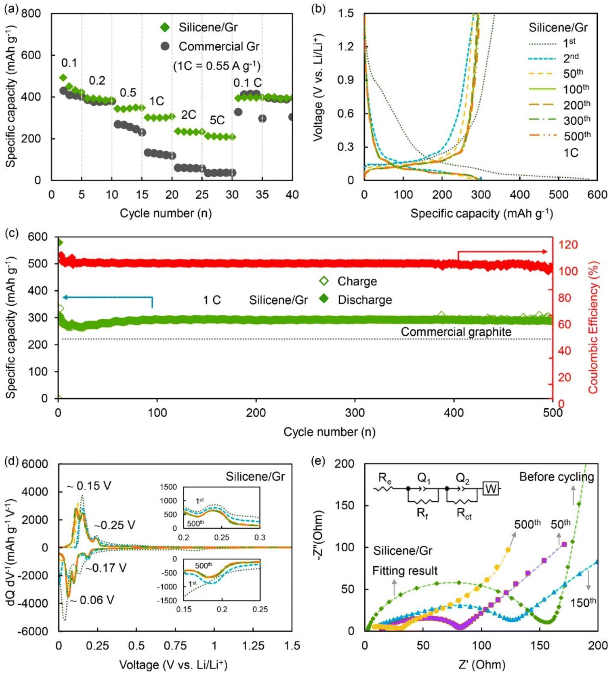
Silicene-based materials are well established as active anode materials for lithium-ion batteries. N-doped silicene is a good n-type material.214 Defective borophene materials show moderate adsorption energy in the range of 1–3 eV to LiSn (lithium polysulfide), which justifies their use to overcome the polysulfide shuttle effect in lithium polysulfide batteries.215 Similarly, group IV elements, i.e., Si, Ge, and Sn-based semiconductive two-dimensional materials, are also pioneered in energy storage devices. Beyond lithium, they have been used in other alkali metals such as sodium and potassium ion batteries and help the pseudo-proton for the dual intercalation process (intercalation and back-intercalation).216 However, few experimental studies have produced silicene monolayer/few layers due to their very complex synthesis process. Yutthanakon et al. reported a chemical exfoliation technique to produce 1.73–3 nm thick silicene via a relatively greener route.63 As shown in Fig. 21, they observed a 306 mA h g−1 discharge capacity at 1C (the amount of electrical current that goes through the battery divided by the area of its layer) rate and approximately 290 mA h g−1 at 1C current density after 500 cycles with 97% retention.63 Furthermore, the CV curves in Fig. 21d show two sets of sharp peaks at ∼0.06 V and ∼0.15 V, corresponding to lithium-ion intercalation and deintercalation in the silicene–graphene anode, respectively.217 This clearly indicates that the composite electrode performs extra functions in the battery. Also, as shown in Fig. 22, the two other peaks at ∼0.17 V and ∼0.25 V clearly represent the phase transition of silicon (Si) to LiSx and LiSx to Si, respectively.
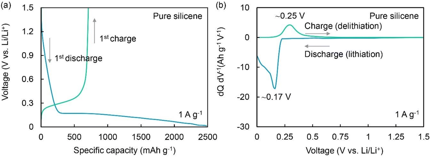 | ||
| Fig. 22 (a) Charge–discharge profile and (b) cyclic voltametric plots of pure silicene, which were used for comparison with the new synthesized material. Reproduced from ref. 63, copyright 2023. | ||
Solid-state-synthesized silicene nanoflowers (SF) were used as an anode for LIBs. Silicene nanoplates formed the flower-like structure (Fig. 23a), which could moderate the irreversible lithium incorporation in the anode surface, which is more beneficial to achieve a high cycle life (1100 mA h g−1 at 2 A g−1 over 600 cycles), high specific capacity (2000 mA h g−1 at 800 mA g−1), specific energy density (543 W h kg−1) and energy density (1257 W h L−1) in an LCO‖SF full cell, which was experimentally higher than that of the LCO‖graphite cell, as shown in Fig. 23b. It showed a good rate capability of 312 mA h g−1 at 5 A g−1 current density (Fig. 23c) and possessed high cycle stability up to 1800 cycles (shown in Fig. 23d).218
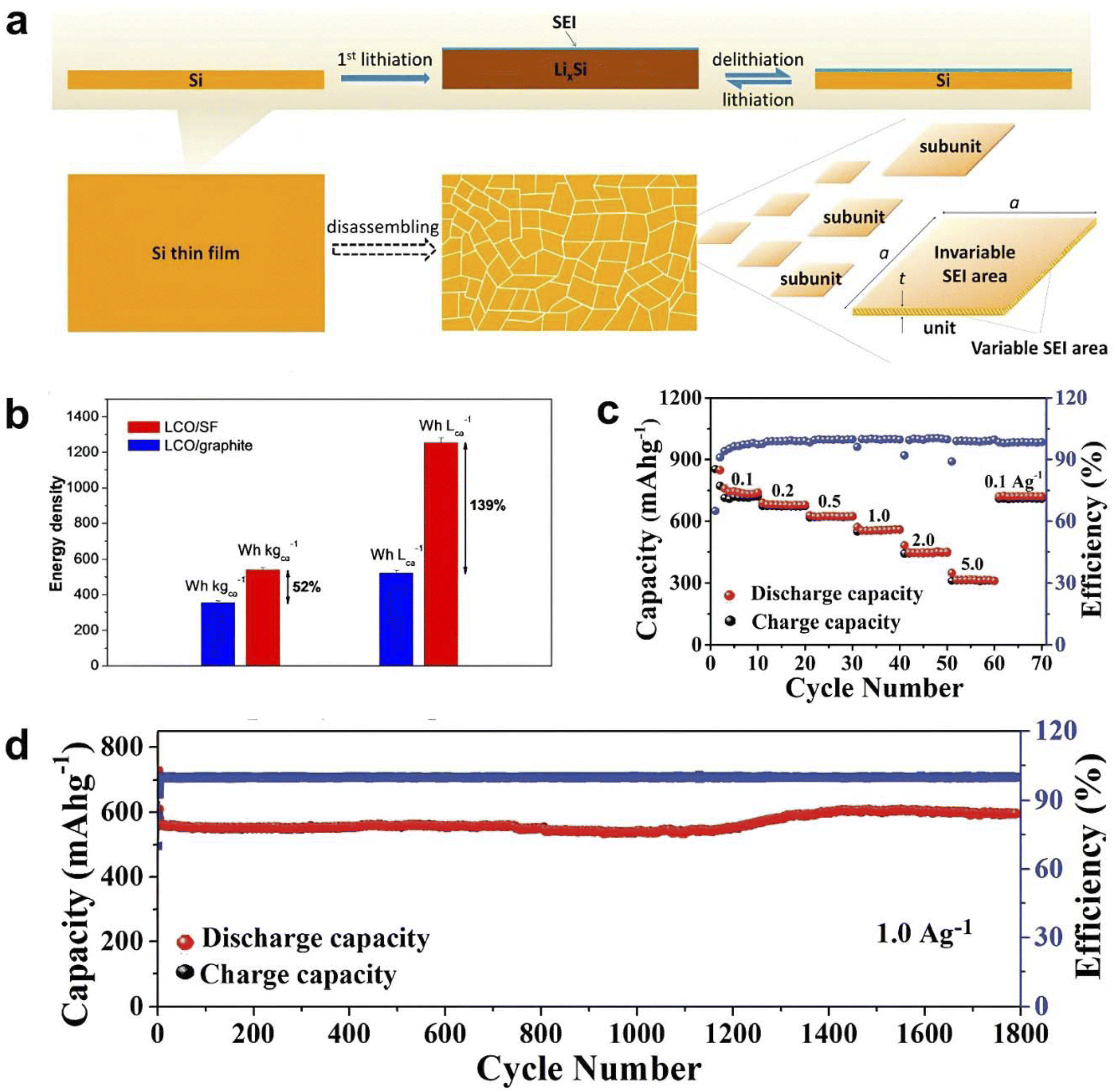 | ||
| Fig. 23 (a) 2D Si blocks disassembled from an Si thin film during the lithiation–delithiation process. Reproduced from ref. 218, copyright 2017. The lateral surface is the limited variable SEI area and the planar surface is the nearly invariable SEI area. (b) Specific energies and energy densities of the LiCoO2/SF and LiCoO2/graphite full cells based on both the cathode and anode,218 copyright 2017. (c) Rate capability of multilayer silicene electrodes in Li metal half cells. Reproduced from,219 copyright 2018. (d) Cycling performance of multilayer silicene electrodes in Li metal half-cells at the current density of 1 A g−1. Reproduced from ref. 219, copyright 2018. | ||
Germanene 2D nanosheet-based materials were explored with sodium-ion batteries. However, isotropic germanene-based anodes have serious issues due to the high diffusion barrier of sodium ions at the hexagonal germanium lattice; rather than an organized and isotropic system, where a defect-rich nanosheet exhibits great affinity towards sodium storage efficiency through the pseudo-intercalation mode with fascinating mechanical flexibility. Recently, Liu et al. presented a defect-mediated active site-containing germanene anode, which had the capability to show 696 mA h g−1 initial energy capacity, 342 mA h g−1 at 0.2 A g−1 rate capacity, and 315 mA h g−1 at 0.1 A g−1 average rate stability.220 These germanene, hydrogenated germanene, and germanium particles showed defined redox peaks in their corresponding CV curves, as shown in Fig. 24(a)–(c), respectively. Among them, germanene nanosheets possessed the highest discharge capacity of 695 mA h g−1 (shown in Fig. 24d). The capacity retention against cycle number is presented in Fig. 24e and at different current densities is shown in Fig. 24f.
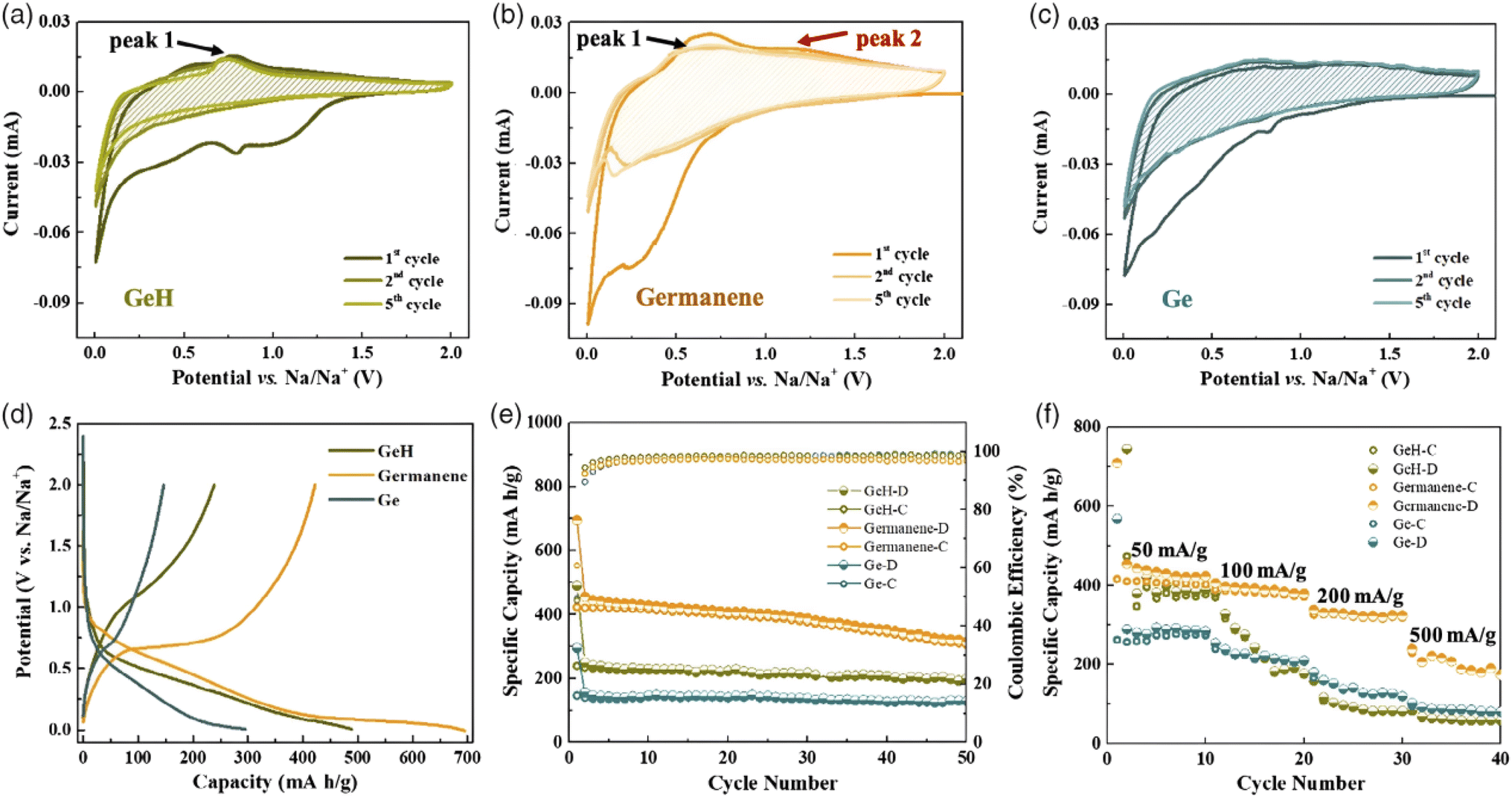 | ||
| Fig. 24 Electrochemical performance of GeH (hydrogenated germanene), germanene, and Ge-based NIBs (sodium ion batteries). (a) Cyclic voltametric profiles of GeH between 0.01 and 2 V at 0.1 mV s−1 scan rate; (b) CV curves of germanene between 0.01 and 2 V at a scan rate of 0.1 mV s−1; (c) cyclic voltametric profiles of Ge between 0.01 and 2 V at 0.1 mV s−1 scan rate; (d) first charge/discharge voltage curves of germanene, hydrogenated germanene and germanium at a rate of 100 mA g−1; (e) stability performances of germanene, hydrogenated germanene and germanium at 100 mA g−1 current density; and (f) rate profile comparison of germanene, hydrogenated germanene, and germanium. Reproduced from ref. 220, copyright 2021. | ||
The electrochemical energy storage properties of stanene were found to be a potential beginning of an updated metallic material structure-lithiated 2D stanene layered sheet (Li5Sn2) with a high specific capacity of 300 mA h g−1 at 74.4 mA g−1 (Fig. 25c) and high cycling rate of 4761 mA g−1 up to 900 cycles (shown in Fig. 25). Here, the battery-like anode also showed a slight pseudocapacitive nature.221 As shown in Fig. 26a, the CV curves are reversible, indicating the good rate capability of these electrodes. This property follows the current density, i = avb equation, where v is the scanning rate (V s−1), and a and b are variable entities. Through logarithmic treatment, Shubin et al. determined the value of b, i.e., 0.737, from the anode hump, which justifies the pseudo-capacity and large cycle number for potassium ion storage.221,222
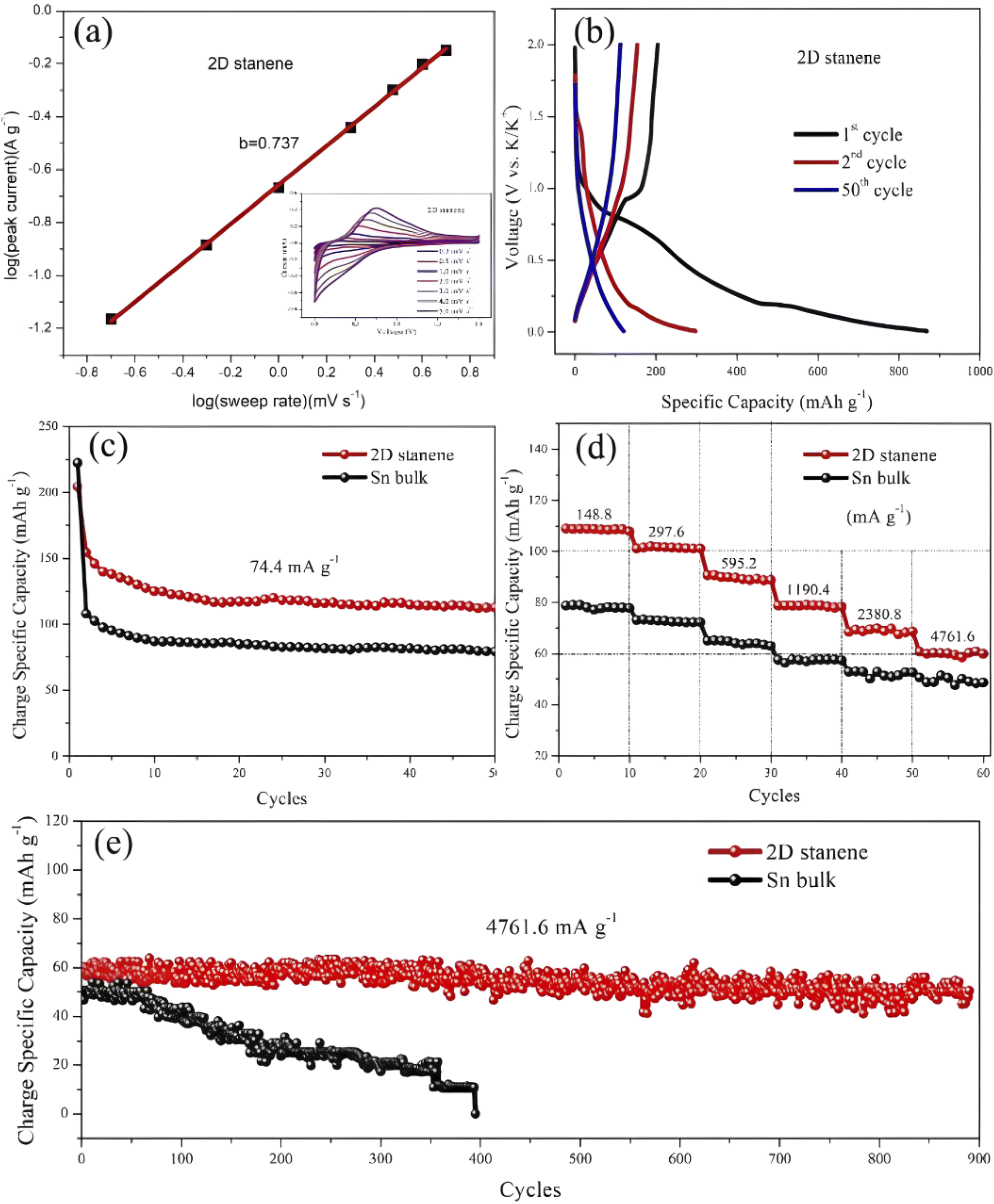 | ||
| Fig. 25 (a) Taffel plot for anodic and the obtained b value (above the line) for 2D stanene anode. (b) First-two and the 50th charge–discharge profile of 2D stanene anode at 74.4 mA g−1 current density. (c) Performance comparison of 2D stanene and Sn bulk anode at 74.4 mA g−1 current density. (d) Rate comparison study of 2D stanene and Sn bulk anode at different current densities from 148.8 mA g−1 to 4761 mA g−1. (e) Continuous cyclic performance comparison of 2D stanene and Sn bulk anode at 4761 mA g−1 current density. Reproduced from ref. 221, copyright 2019. | ||
 | ||
| Fig. 26 Electrochemical characterization of few-layer bismuthene-graphene. (a) Cross-sectional SEM image compiled with a digital photograph of few-layer bismuthene-graphene film. (b) Cyclic voltametric profile of the FLB-G electrode at 0.1 mV s−1 between 0.1 and 2.1 V. (c) Galvanostatic intermittence titration technique curves at the fifth cycle for few-layer bismuthene-graphene. (d) Specific capacity, coulombic efficiency and electrochemical rate performance of few-layer bismuthene-graphene film and graphene films at various current densities from 0.2 to 2.0 mA cm−2. (e) Cyclability of few-layer bismuthene-graphene film at 1.2 mA cm−2 current density after 20-cycle electrochemical pretreatment at 0.05 mA cm−2. Reproduced from ref. 225, copyright 2019. | ||
A monolayer of honeycomb aluminium lattice shows very interesting adsorption affinity towards metal ions such as Li, Na, K, and Ca and a very low surface diffusion barrier of 0.03 eV for Li and 0.42 for Na, which is very appreciable for the reverse intercalation process. The calculated specific capacity was estimated to be 994 mA h g−1 for Li and 870 mA h g−1 for Na.223
Arsenene monolayers have also been found to be a good accommodator for Mg ions and much better than conventional magnesium metal anodes. Arsenene has a specific capacity of 1429.41 mA h g−1 and a very low barrier for surface monolayer adsorption in the range of 0.82–2.48 eV theoretically, which is in the suitable region.224 The exclusively high theoretical volumetric capacity and relatively low working potential of bismuthene make it a promising anode material. Few-layer bismuthene relieves expansion strain. Practically, a bismuthene-graphene composite achieved a sodium storage capacity of 12.1 mA h cm−2, which is truly remarkable. A few-layer bismuthene-graphene composite electrode achieved a stable capacity of 381 mA h g−1 at a current density of 0.2 mA cm−2 and could maintain a high reversible capacity of 263.2 mA h g−1 at 2 mA cm−2 current density, where that of pure graphene is 3.4 mA h g−1 under the same condition. Here, the volume expansion plays a major role in large cycle number stability and its rational hybridization with graphene. It acts as an elastic buffer, accommodating the large volume change and high conductivity of the composite film.225 As shown in Fig. 26, the first cycle has a broad peak in the reduction region due to the sodiation of bismuth and formation of a solid electrolyte film. After the first cycle, two distinct peak couples were observed at 0.64/0.75 and 0.43/0.62 V due to the reversible formation of NaBi and Na3Bi, respectively.226 The sodiation and desodiation processes were probed through the galvanostatic intermittent titration technique, where the voltage variation plateau was very small, and the sodiation–desodiation process was very fast, as shown in Fig. 26c. Also, at different current densities, it showed a good capacity retention and rate performance (Fig. 26d). Finally, the results showed the long-term reversible capacity of 317 mA h g−1 at 1.2 A g−1 current densities for 1000 cycles onwards (Fig. 26e). Presently, there are still critical challenges in the real-time application of Xenes as prototypes or in device fabrication. Graphene possesses extraordinary stability due its sp2 hybridization, but in general, Xenes face serious problems such as chemical reactivity with neighbouring species under ambient conditions. Different chemical encapsulation methods have been adopted towards a chemical view to protect them from moisture or free oxygen molecules of air,240 which definitely contributes additional complexity in the device fabrication and cost.
A list of energy-related applications employing Xenes is presented in Table 1.
| Sl. No. | Material | Potential energy applications | Reference |
|---|---|---|---|
| 1 | Borophene | HER | 153 |
| CO2RR | 228 | ||
| N2 RR | 141 | ||
| Li-ion & Na-ion battery | 229 | ||
| Li–S battery | 215 | ||
| Supercapacitor | 230 | ||
| 2 | Graphene | HER | 47 |
| OER | 231 | ||
| ORR | 232 | ||
| N2RR | 233 | ||
| NO3RR | 234 | ||
| CO2RR | 235 | ||
| Electrode designing | 236 | ||
| All weather super-batteries | 237 | ||
| Supercapacitors | 238 | ||
| 3 | Aluminene | Anode material for Li-ion and Na-ion batteries | 223 |
| 4 | Silicene | HER | 158 |
| N2RR | 239 | ||
| HER & OER | 159 | ||
| Zinc ion capacitor | 240 | ||
| Lithium–oxygen batteries | 241 | ||
| 5 | Phosphorene | HER | 242 |
| Electrochemical CO reduction | 243 | ||
| N2RR | 244 | ||
| Cathode material in Na-ion battery | 100 | ||
| Anode material for the rechargeable Li ions | 245 | ||
| Supercapacitor | 246 | ||
| 6 | Sulfurene | Not currently explored | NA |
| 7 | Gallenene | Na-ion battery | 247 |
| Electrocatalysis | 247 | ||
| 8 | Germanene | HER | 158 |
| Photo/electrocatalyst | 248 | ||
| Lithium-ion battery | 249 | ||
| Sodium-ion battery | 250 | ||
| 9 | Arsenene | HER | 251 |
| N2RR | 252 | ||
| Photocatalytic water splitting | 253 | ||
| Li/Na/Mg-ion battery | 254 | ||
| 10 | Selenene | Not currently explored | NA |
| 11 | Indiene | Not currently explored | NA |
| 12 | Stanene | CO2RR | 255 |
| N2RR | 256 | ||
| Na-ion battery | 257 | ||
| 13 | Antimonene | Photo/bio-catalytic CO2RR | 258 |
| Energy storage | 259 | ||
| 14 | Tellurene | Photocatalytic HER | 260 |
| Li–S battery | 261 | ||
| Alloy with alkali metals for battery application | 262 | ||
| 15 | Thallene | Not currently explored | NA |
| 16 | Plumbene | Not currently explored | NA |
| 17 | Bismuthene | Photocatalytic HER | 263 |
| CO2RR | 264 | ||
| 143 | |||
| Electrocatalytic CO2RR to liquid fuels | 182 | ||
| Li-ion battery | 265 | ||
| Na-ion battery | 225 | ||
| K-ion battery | 266 | ||
| 18 | Poloniumene | Not currently explored | NA |
4. Challenges and future prospects
A thorough examination of the barriers and limitations preventing the development of 2D materials in useful devices is essential, although the examined works offered insightful information into the potential of these materials. Thus, by outlining the main challenges faced during the synthesis, long-term stability, and device integration of these promising materials, this section seeks to close this crucial gap.4.1 Synthesis
The scalable and controlled production of high-quality 2D materials continues to face several obstacles. The poor yields, irregular morphology, and impurity inclusions of current technologies hamper the performance and repeatability of devices. For example, the electrical characteristics of layered materials such as graphene can be affected by the presence of flaws and edge roughness introduced by exfoliation.267 Furthermore, synthesizing some 2D materials from the bottom up frequently necessitates severe growth conditions (such as elevated temperatures and hazardous chemicals) that are not conducive to large-scale production and restrict the incorporation of these substances with different device materials.268 The largest problem of the modern period is the adoption of future industrial advances, such as large-scale integrated circuit production and two-dimensional material (2D) wafer size. Large surface areas and superior-quality nanocrystals are needed for 4th generation optoelectronic technology. Substantial attempts have been undertaken to create materials with huge dimensions, controlled thicknesses, parallel crystal domains, and a few flaws that can be automatically thinned into two-dimensional sheets. The remarkable mechanical, thermal, and optoelectric characteristics of 2D materials have received significant attention lately. Therefore, further research is required to properly synthesize and fabricate laminar 2D nanomaterials and integrate them into a wide range of applications.2694.2 Long-term stability
There is still much uncertainty regarding the durability of 2D materials in practical settings. The characteristics of the material can be weakened by exposure to external elements such as moisture, air, and light, which can decrease performance and cause device failure. For example, oxidation may cause considerable changes to the electrical characteristics of some 2D materials, such as transition metal dichalcogenides. These stability difficulties must be resolved for 2D-material-based systems to perform consistently in the long term.270,271 One of the main challenges in practical use is the oxidation and degrading effects that many 2D materials with atomic-scale thicknesses suffer from in ambient settings. Numerous prevention techniques have been proposed and investigated with encouraging results, and research on oxidation and degradation pathways is still in progress. Utilizing theoretical findings and experimental observations to shed light on the oxidation and degradation mechanisms of 2D materials, specifically TMDCs, and BP, in an ambient environment summarizes the most recent passivation techniques and their corresponding protection tactics.2714.3 Device integration
There are several obstacles to overcome when incorporating 2D materials into working devices. Poor interfacing with other device components, such as electrodes and dielectrics, is frequently caused by the incompatibility of these atomically thin layers with traditional device topologies. Problems, including contact resistance, charge traps, and decreased device performance, may result from this. Further impeding the functionality of the device is the potential presence of flaws and contamination during the transfer of 2D materials from their growth substrate to the intended device platform. Reaching the full potential of 2D materials in a range of technological applications requires overcoming these integration obstacles.272,273 Because 2D monolayers lack surface dangling connections, they interact with each another via van der Waals forces. Without the need for lattice matching or direct chemical bonding, this property makes it possible to combine any two-dimensional (amorphous or crystalline) material with another two-dimensional (crystalline or non-2D) material in a single step.274 For various sophisticated next-generation photodetection uses, recently found 2D materials with their distinct qualities and functions may be coupled with 0D, 1D, or 3D materials to create heterostructures of various dimensions.274 High processing temperatures are often required for the synthesis of high-quality 2D materials, which increase the difficulty of direct wafer growth, thus making transfer technology more attractive. Wafer bonding technology may, in principle, be able to solve this problem; however, it is clear that the production capacity of this technology is not yet ideal. Controlling dielectric and contact interfaces is difficult for 2D materials at the device level. Given that the surfaces of 2D materials are self-passivating, dielectric deposition must be achieved through manufacturing techniques such as atomic layer deposition. Compared to the best laboratory demonstrations using crystalline 2D insulators (e.g., hexagonal boron nitride), the non-ideal interfaces of the latter limit the device performance.275,276An exciting period of technological innovation and development has been made possible by ground-breaking discoveries in the analysis of two-dimensional (2D) materials. The investigation of additional 2D elements, including borophene, aluminene, silicene, germanene, stanene, phosphorene, arsenene, antimonene, and bismuthene, has been made possible by graphene, a pioneer in this field. Thorough analysis showed the special properties and potential uses of these materials in biomedicine, electronics, optoelectronics, and energy storage, and other fields. In the near future, creating innovative technologies and gadgets may be facilitated by a thorough understanding of their qualities and uses.
(I) Graphene has been the focus of many studies due to its exceptional mechanical, electrical, and thermal properties.277 Due to its remarkable properties, including fast electron mobility, excellent thermal conductivity, and incredible mechanical strength, the field of electronics has produced extremely fast and low-power electronic devices.277 As this field has progressed, other 2D materials have emerged as strong contenders in the electronics arena, each with unique properties. Borophene, a 2D allotrope of boron, has recently gained significant attention due to its metallic properties and high electron mobility.20 These properties make borophene a promising material for next-generation electronic devices, especially in high-frequency transistors and interconnects.278,279 Similarly, aluminene, a 2D form of aluminium, exhibits interesting electronic properties, such as tunable bandgap, making it a valuable candidate for various optoelectronic applications.280,281 With its highly desirable electrical properties, silicene rapidly becomes a two-dimensional material with various uses. It is especially promising for use in silicon-based nano-electronics. Theoretical investigations initially predicted a honeycomb structure with similar electrical properties to graphene. Although these investigations focused on free-standing silicene, epitaxial growth on crystal surfaces is the only experimental method used to produce silicene. Strong silicene-metal interactions influence the electrical properties of epitaxially grown silicene on metal surfaces.282 Zhang et al.283 used first-principles techniques to study the structural and electrical properties of silicene/silicene and silicene/germanene heterobilayers (HBLs). The results indicate a weak van der Waals contact between silicene and the substrate, with an overall binding energy of −50 to −70 meV per Si (Ge) atom when silicene interacts with silicane (germanene). Silicene is expected to help create a high-performance FET channels, expanding its potential applications in future nanoelectronics.
(II) Optoelectronics, which combines electronics and light, has also benefited greatly from 2D materials. Black phosphorus in two dimensions, phosphorene, has generated interest because of its inherent bandgap that can be adjusted by changing the number of layers.284 Due to its special properties, phosphorene is an attractive alternative material for the fabrication of solar cells, LEDs, and photodetectors. Phosphorene is a flexible material for various optoelectronic applications due to its configurable bandgap, which offers more design and performance optimization options.284 Antimonene is a newly discovered 2D substance that has become prominent very quickly because of its special optical and electrical capabilities.285,286 Both theoretical and experimental research confirmed its exceptional semiconducting features, including an adjustable band gap, high carrier mobility, low thermal conductivity, and improved optical responsiveness. These qualities are intriguing for real-world applications in a variety of areas. According to theoretical predictions made by Zeng and colleagues,287 semiconductors with a broad-band gap range of 2.28 eV can be created by reducing semimetal bulk Sb to a single atomic layer. Furthermore, they discovered that by altering the O concentration, antimonene oxides with directly adjustable band gaps and high carrier mobility can be produced, which may offer desirable characteristics for optoelectronics applications.
(III) 2D materials are beginning to appear in practical applications beyond the domain of scholarly study. For example, transparent conductive films and graphene-based touch screens are currently available for sale and incorporated in consumer devices such as tablets and smartphones.288 These uses take advantage of the unique electrical conductivity and transparency of graphene to create touch screens that are more robust and responsive. The consumer electronics sector is predicted to undergo a transformation as 2D materials are more widely adopted in commercial devices due to their increasing affordability and large-scale manufacturing capabilities.288
(IV) 2D materials offer a rich investigation opportunity in energy harvesting and conversion. The significant light-absorbing capacity of 2D materials can be used by photovoltaic devices such as solar cells to produce light and more efficient solar panels. Furthermore, due to their high surface area and electrical conductivity, 2D materials can be employed in advanced energy storage and conversion devices such as supercapacitors and batteries, which can greatly improve the performance and advance the development of renewable energy technologies.289,290 In the field of materials research, graphene is a fast-emerging superstar. The unique characteristics of this two-dimensional material include good mechanical and chemical stability, outstanding optical transmittance, and low resistance. These remarkable benefits hold considerable potential for their possible integration into solar energy systems.291 Graphene links could be formed via the anchoring of nanocrystalline TiO2 on graphene flakes. Due to its superior electrical conduction, bridge graphene can promote charge separation by reducing the charge recombination and speeding up electron transit from the conduction band (CB) of TiO2 at the anchor place, creating the perfect two-dimensional material for flexible solar cell electrodes.292 Chen and colleagues292 presented an incredibly straightforward, independent solar energy converter that requires a pre-prepared 3D cross-linked honeycomb graphene foam material and no further supporting elements. This comprehensive, straightforward material has the potential to function as the perfect solar thermal converter, which can absorb and transform sunlight into heat. Subsequently, this heat can be used to turn water from numerous sources into steam and create pure water in surrounding settings with extremely high effectiveness and minimal solar flux. Another newly developed 2D material, borophene, exhibits exceptional light absorption characteristics surpassing that of graphene. Its distinct structure and adjustable band gap provide intriguing opportunities to overcome the restrictions in existing solar cell technology.293 The inclusion of borophene in cellulose nanofibers (CNF) was reported by Guan et al.,294 allowing good environmental stability during modelled sunshine with an outstanding light-to-heat conversion efficiency of 91.5% and a water evaporation rate of 1.45 kg m−2 h−1. Additionally, during three sun irradiations, it was shown that borophene sheets may be used as an outstanding active photothermal material to eliminate about 100% of Gram-positive and Gram-negative bacteria in just 20 min. These results provide new opportunities for developing borophene-based sheets with special photothermal qualities that may be applied to efficiently treat various wastewaters.
(V) A new chapter in biomedical applications has begun with the development of 2D materials, which offer stimulating potential for multidisciplinary innovation and progress. Thanks to their unique physicochemical properties, 2D materials have shown great potential for various biomedical applications such as drug delivery, tissue engineering, biosensing, and bioimaging. These materials have the potential to transform clinical practice and biological research by addressing some of the most important issues in contemporary health care, such as early disease diagnosis, tailored treatment, and targeted drug delivery.295 The biomedical profession has shown great interest in graphene, in particular, because of its remarkable mechanical strength, large surface area, and biocompatibility.296 2D materials have shown significant potential in cancer therapy by allowing individualized and targeted treatment planning. For example, functionalized graphene-based nano-carriers have been shown to be highly effective in delivering therapeutic drugs to cancer cells with little off-target effects and systemic toxicity.297 Borophene is gaining attention due to its unique chemical and physical properties that can be harnessed in biomedicine.298–300
(VI) Significant potential has also been shown by 2D materials in applications related to sensing and detection. Because of its unique surface reactivity and customizable electrical properties, borophene has gained much interest and can be used in advanced chemical and gas sensors.279,299 Because borophene-based sensors have high sensitivity to a wide range of gas and chemical species, they are an important component of next-generation sensing technologies for industrial safety and air-quality monitoring. These sensors can detect hazardous gases and other environmental contaminants. Aluminene has shown potential in sensing applications, particularly in detecting hazardous chemicals and volatile organic compounds (VOCs).301,302 For instance, functionalized graphene-based biosensors have demonstrated high sensitivity and specificity in detecting various biomarkers and disease indicators.303
(VII) The science of energy conversion and storage is undergoing a significant transformation, and 2D materials will be critical in shaping this future. Graphene, a single layer of carbon atoms organized into a two-dimensional honeycomb lattice, has transformed the field of energy conversion and storage due to its remarkable mechanical strength, large surface area, and electrical conductivity.2 These properties have created new opportunities for high-performance energy storage technologies, including batteries and supercapacitors. Furthermore, to enable more efficient and sustainable energy technologies, graphene-based materials are being investigated as state-of-the-art catalysts for fuel cells and other energy conversion processes.288
5. Conclusion
In conclusion, the discovery of graphene marked a pivotal moment in the world of science, offering diverse applications that have revolutionized various industries. However, this story does not end with graphene; over the past decade, a remarkable array of novel 2D materials (Xenes), closely related to graphene, has emerged. The materials discussed in the article belong to groups 13, 14, 15, and 16 of the periodic table, which exhibit unique properties and hold great potential for energy-related applications, such as catalysis, supercapacitors, and batteries. These 2D materials possess attributes that are highly attractive for energy functions, including substantial surface area, mechanical properties, and excellent thermal and electrical conductivity. They are particularly well-suited for catalysis, offering many active sites, and are integral to the development of green catalysis, which is closely related to hydrogen generation and utilization. Moreover, these materials show promise in supercapacitors, with their fast charging and discharging capabilities, and in batteries, offering high energy density and ion storage capacity.As we look toward a future where sustainable energy sources such as hydrogen and solar power play an essential role, these 2D materials represent a promising alternative to graphene-based systems. The remarkable properties of these materials and their potential are paving the way for innovative and eco-friendly energy solutions. This work underscores the exciting prospects of integrating emerging 2D materials into the world of energy materials, presenting a pathway toward a greener and cleaner future for humanity.
Abbreviations
| MXene | Metal-Xene |
| HER | Hydrogen evolution reaction |
| HOR | Hydrogen oxidation reaction |
| OER | Oxygen evolution reaction |
| CO2RR | Carbon dioxide reduction reaction |
| NRR | Nitrogen reduction reaction |
| DMF | Dimethylformamide |
| IPA | Isopropyl alcohol |
| PXRD | Powder X-ray diffraction |
| XRD | X-ray diffraction |
| SEM | Scanning electron microscope |
| TEM | Transmission electron microscope |
| T c | Crystallization temperature |
| K | Kelvin's scale |
| °C | Degree Celsius |
| UV spectra | Ultraviolet-visible spectra |
| eV | Electron volt |
| DFT | Density functional theory |
| Si | Silicon |
| SiO2 | Silicon oxide |
| Ga | Gallium |
| nm | Nanometre |
| MoS2 | Molybdenum disulphide |
| meV | Milli electron volt |
| SiC | Silicon carbide |
| Ar | Argon |
| C | Carbon |
| QSHI | Quantum-spin hall insulator |
| Tl | Thallium |
| NiSi2 | Nickel silicide |
| UHV | Ultrahigh vacuum |
| LEED | Low energy electron diffraction |
| ARPES | Angle resolved photoemission spectroscopy |
| Å | Angstrom |
| GO | Graphene oxide |
| CNT | Carbon nanotube |
| SLG | Single layer graphene |
| BLG | Bi-layer graphene |
| TPa | Tera pascal |
| GNRs | Graphene nanoribbons |
| ZrB2 | Zirconium diboride |
| Ag | Argentum |
| TI-FETs | Topological insulator field-effect transistors |
| Li | Lithium |
| Pt | Platinum |
| Ge | Germanium |
| SOC | Spin–orbit coupling |
| GeH | Germanane |
| Ti | Titanium |
| V | Vanadium |
| Cr | Chromium |
| Sn | Stannum |
| E | Young's modulus |
| UTS | Ultimate tensile strength |
| ν | Poisson's ratio |
| N m−1 | Newton per metre |
| MBE | Molecular beam epitaxy |
| WF | Wiedemann–Franz |
| K e | Electron thermal conductivity |
| K ph | Phonon thermal conductivity |
| Al2O3 | Aluminium oxide |
| Pd | Palladium |
| Pb | Plumbum |
| Ir | Iridium |
| Fe | Iron |
| BP | Black phosphorous |
| GPa | Gigapascal |
| Rh | Rhodium |
| HRTEM | High-resolution transmission electron microscope |
| MoS2 | Molybdenum disulphide |
| WSe2 | Tungsten diselenide |
| SW | Stone–Wales defect |
| DV | Double vacancy defect |
| CPMD | Car–Parrinello molecular dynamics |
| AS2O3 | Arsenic trioxide |
| 2θ | Bragg's angle |
| As | Arsenic |
| LPE | Liquid phase epitaxy |
| Rpm | Revolutions per minute |
| Sb | Antimony |
| Bi | Bismuth |
| HRXRD | High-resolution X-ray diffraction |
| XPS | X-ray photoelectron spectroscopy |
| AFM | Atomic force microscopy |
| Se | Selenium |
| PVD | Physical vapor deposition |
| SeO2 | Selenium dioxide |
| Te | Tellurium |
| CO | Carbon monoxide |
| N2RR | Nitrogen reduction reaction |
| H2 | Hydrogen |
| H2O | Water |
| CVD | Chemical vapor deposition |
| Mn | Manganese |
| Co | Cobalt |
| Ru | Ruthenium |
| NH3 | Ammonia |
| MOF | Metal–organic framework |
| CO2 | Carbon dioxide |
| EV | Electro voltaic |
| ELDC | Electrochemical double layer capacitor |
| S m−1 | Siemens per meter |
| H2SO4 | Sulfuric acid |
| mV s−1 | Millivolt per second |
| W kg−1 | Watt per kilogram |
| F g−1 | Farad per gram |
| A g−1 | Ampere per gram |
| IL | Ionic liquid |
| mA h g−1 | Milliampere-hours per gram mass |
| Mg+ | Magnesium ion |
| K+ | Potassium ion |
| Ca+ | Calcium ion |
| Na+ | Sodium ion |
| LIB | Lithium-ion battery |
| ML | Machine learning |
| CV | Cyclic voltammetry |
| SF | Silicene nano flower |
| LiCoO2 | Lithium cobalt oxide |
| SEI | Solid electrolyte interface |
| NIB | Sodium ion batteries |
| FLB-G | Few layered bismuthene-graphene |
| TMDCs | Transition metal dichalcogenide monolayers |
| HBLs | Heterobilayers |
| FET | Field effect transistor |
| LED | Light emitting diode |
| CB | Conduction band |
| TiO2 | Titanium oxide |
| CNF | Cellulose nanofibers |
| VOCs | Volatile organic compounds |
| Po | Polonium |
Author contributions
Sumon Santra: writing – original draft, formal analysis, visualization, conceptualization. Bishwajit Das: writing – original draft, formal analysis, visualization, conceptualization. Anuraag Ghosh: writing – original draft, formal analysis, visualization, conceptualization. Shibam Pal: writing – original draft, formal analysis, visualization, conceptualization. Saikat Pal: writing – original draft, formal analysis, visualization, conceptualization, supervision. Ashadul Adalder: writing – original draft, review & editing, supervision.Conflicts of interest
The authors declare that they have no known competing financial interests or personal relationships that could have appeared to influence the work reported in this paper.Acknowledgements
We acknowledge Dr Uttam Kumar Ghorai and Ramakrishna Mission Vidyamandira for their thorough support for all kinds of assistance.References
- G. Sanchit, Batteryless Mobile using Supercapacitor with Wireless Charging, Int. J. Res. Appl. Sci. Eng. Technol., 2017, 810–814, DOI:10.22214/ijraset.2017.3152.
- K. S. Novoselov, A. K. Geim, S. V. Morozov, D. Jiang, Y. Zhang, S. V. Dubonos, I. V. Grigorieva and A. A. Firsov, Electric field in atomically thin carbon films, Science, 2004, 306, 666–669, DOI:10.1126/SCIENCE.1102896/SUPPL_FILE/NOVOSELOV.SOM.PDF.
- M. E. Dávila and G. Le Lay, Silicene: genesis, remarkable discoveries, and legacy, Mater. Today Adv., 2022, 16, 100312, DOI:10.1016/J.MTADV.2022.100312.
- A. Molle, J. Goldberger, M. Houssa, Y. Xu, S. C. Zhang and D. Akinwande, Buckled two-dimensional Xene sheets, Nat. Mater., 2017, 16, 163–169, DOI:10.1038/nmat4802.
- C. Grazianetti and C. Martella, The Rise of the Xenes: From the Synthesis to the Integration Processes for Electronics and Photonics, Materials, 2021, 14, 4170, DOI:10.3390/MA14154170.
- I. I. Izhnin, K. R. Kurbanov, K. A. Lozovoy, A. P. Kokhanenko, V. V. Dirko and A. V. Voitsekhovskii, Epitaxial fabrication of 2D materials of group IV elements, Appl. Nanosci., 2020, 10, 4375–4383, DOI:10.1007/S13204-020-01372-4/METRICS.
- A. Molle and C. Grazianetti, Xenes: 2D Synthetic Materials Beyond Graphene, 2022 Search PubMed.
- A. Zhao and B. Wang, Two-dimensional graphene-like Xenes as potential topological materials, APL Mater., 2020, 8, 030701, DOI:10.1063/1.5135984/594618.
- K. S. Novoselov, D. Jiang, F. Schedin, T. J. Booth, V. V. Khotkevich, S. V. Morozov and A. K. Geim, Two-dimensional atomic crystals, Proc. Natl. Acad. Sci. U. S. A., 2005, 102, 10451–10453, DOI:10.1073/PNAS.0502848102/ASSET/42E09135-5FC8-49D9-9A4F-EC8415C3CDE5/ASSETS/GRAPHIC/ZPQ0290589320003.JPEG.
- N. R. Glavin, R. Rao, V. Varshney, E. Bianco, A. Apte, A. Roy, E. Ringe and P. M. Ajayan, Emerging Applications of Elemental 2D Materials, Adv. Mater., 2020, 32, 1904302, DOI:10.1002/ADMA.201904302.
- H. Zhang, Ultrathin Two-Dimensional Nanomaterials, ACS Nano, 2015, 9, 9451–9469, DOI:10.1021/acsnano.5b05040.
- Y. Zheng, Y. Jiao, L. Ge, M. Jaroniec and S. Z. Qiao, Two-Step Boron and Nitrogen Doping in Graphene for Enhanced Synergistic Catalysis, Angew. Chem., Int. Ed., 2013, 52, 3110–3116, DOI:10.1002/ANIE.201209548.
- L. Qu, Y. Liu, J.-B. Baek and L. Dai, Nitrogen-Doped Graphene as Efficient Metal-Free Electrocatalyst for Oxygen Reduction in Fuel Cells, ACS Nano, 2010, 4, 1321–1326, DOI:10.1021/nn901850u.
- E. Yoo, J. Kim, E. Hosono, H. Zhou, T. Kudo and I. Honma, Large Reversible Li Storage of Graphene Nanosheet Families for Use in Rechargeable Lithium Ion Batteries, Nano Lett., 2008, 8, 2277–2282, DOI:10.1021/nl800957b.
- S. Balendhran, S. Walia, H. Nili, S. Sriram and M. Bhaskaran, Elemental Analogues of Graphene: Silicene, Germanene, Stanene, and Phosphorene, Small, 2015, 11, 640–652, DOI:10.1002/SMLL.201402041.
- M. Pumera and Z. Sofer, 2D Monoelemental Arsenene, Antimonene, and Bismuthene: Beyond Black Phosphorus, Adv. Mater., 2017, 29, 1605299, DOI:10.1002/ADMA.201605299.
- Z. Huang, X. Qi and J. Zhong, 2D Monoelemental Materials (Xenes) and Related Technologies, 2022, DOI:10.1201/9781003207122/2D-MONOELEMENTAL-MATERIALS-XENES-RELATED-TECHNOLOGIES-ZONGYU-HUANG-XIANG-QI-JIANXIN-ZHONG.
- E. Martínez-Periñán, M. P. Down, C. Gibaja, E. Lorenzo, F. Zamora and C. E. Banks, Antimonene: A Novel 2D Nanomaterial for Supercapacitor Applications, Adv. Energy Mater., 2018, 8, 1702606, DOI:10.1002/AENM.201702606.
- A. K. Tareen, K. Khan, M. Aslam, H. Zhang and X. Liu, Recent progress, challenges, and prospects in emerging group-VIA Xenes: synthesis, properties and novel applications, Nanoscale, 2021, 13, 510–552, 10.1039/D0NR07444F.
- A. J. Mannix, X. F. Zhou, B. Kiraly, J. D. Wood, D. Alducin, B. D. Myers, X. Liu, B. L. Fisher, U. Santiago, J. R. Guest, M. J. Yacaman, A. Ponce, A. R. Oganov, M. C. Hersam and N. P. Guisinger, Synthesis of borophenes: anisotropic, two-dimensional boron polymorphs, Science, 2015, 350, 1513–1516, DOI:10.1126/SCIENCE.AAD1080/SUPPL_FILE/MANNIX.SM.PDF.
- P. Ranjan, T. K. Sahu, R. Bhushan, S. S. Yamijala, D. J. Late, P. Kumar and A. Vinu, Borophene: Freestanding Borophene and Its Hybrids (Adv. Mater. 27/2019), Adv. Mater., 2019, 31, 1970196, DOI:10.1002/ADMA.201970196.
- C. Hou, G. Tai, Z. Wu and J. Hao, Borophene: Current Status, Challenges and Opportunities, Chempluschem, 2020, 85, 2186–2196, DOI:10.1002/CPLU.202000550.
- H. Li, L. Jing, W. Liu, J. Lin, R. Y. Tay, S. H. Tsang and E. H. T. Teo, Scalable Production of Few-Layer Boron Sheets by Liquid-Phase Exfoliation and Their Superior Supercapacitive Performance, ACS Nano, 2018, 12, 1262–1272, DOI:10.1021/ACSNANO.7B07444/SUPPL_FILE/NN7B07444_SI_001.PDF.
- A. Joshi, A. K. Tomar, G. Singh and R. K. Sharma, Engineering oxygen defects in the boron nanosheet for stabilizing complex bonding structure: an approach for high-performance supercapacitor, Chem. Eng. J., 2021, 407, 127122, DOI:10.1016/J.CEJ.2020.127122.
- N. Taşaltın, C. Taşaltın, S. Güngör, S. Karakuş, İ. Gürol and M. Teker, Volatile organic compound detection performance of Borophene and PANI:β Borophene nanocomposite-based sensors, J. Mater. Sci.: Mater. Electron., 2022, 33, 24173–24181, DOI:10.1007/S10854-022-09109-5/METRICS.
- Q. Fan, C. Choi, C. Yan, Y. Liu, J. Qiu, S. Hong, Y. Jung and Z. Sun, High-yield production of few-layer boron nanosheets for efficient electrocatalytic N2 reduction, Chem. Commun., 2019, 55, 4246–4249, 10.1039/C9CC00985J.
- R. C. Xiao, D. F. Shao, W. J. Lu, H. Y. Lv, J. Y. Li and Y. P. Sun, Enhanced superconductivity by strain and carrier-doping in borophene: a first principles prediction, Appl. Phys. Lett., 2016, 109, 122604, DOI:10.1063/1.4963179/32229.
- B. Aziz, A. S. Asha and M. A. Ali, Evaluation of mechanical properties of borophene nanotube by molecular dynamics simulation, AIP Conf. Proc., 2021, 2324, 030022, DOI:10.1063/5.0037898/1027383.
- A. A. Kistanov, Y. Cai, K. Zhou, N. Srikanth, S. V. Dmitriev and Y. W. Zhang, Exploring the charge localization and band gap opening of borophene: a first-principles study, Nanoscale, 2018, 10, 1403–1410, 10.1039/C7NR06537J.
- J. Yuan, N. Yu, K. Xue and X. Miao, Stability, electronic and thermodynamic properties of aluminene from first-principles calculations, Appl. Surf. Sci., 2017, 409, 85–90, DOI:10.1016/J.APSUSC.2017.02.238.
- K. A. Lozovoy, I. I. Izhnin, A. P. Kokhanenko, V. V. Dirko, V. P. Vinarskiy, A. V. Voitsekhovskii, O. I. Fitsych and N. Y. Akimenko, Single-Element 2D Materials beyond Graphene: Methods of Epitaxial Synthesis, Nanomaterials, 2022, 12, 2221, DOI:10.3390/nano12132221.
- C. Kamal, A. Chakrabarti and M. Ezawa, Aluminene as highly hole-doped graphene, New J. Phys., 2015, 17, 083014, DOI:10.1088/1367-2630/17/8/083014.
- M. Petrov, J. Bekaert and M. V. Milošević, Superconductivity in gallenene, 2d Mater, 2021, 8, 035056, DOI:10.1088/2053-1583/AC0713.
- M. Nakhaee, M. Yagmurcukardes, S. A. Ketabi and F. M. Peeters, Single-layer structures of a100- and b010-Gallenene: a tight-binding approach, Phys. Chem. Chem. Phys., 2019, 21, 15798–15804, 10.1039/C9CP02515D.
- V. Kochat, A. Samanta, Y. Zhang, S. Bhowmick, P. Manimunda, S. A. S. Asif, A. S. Stender, R. Vajtai, A. K. Singh, C. S. Tiwary and P. M. Ajayan, Atomically thin gallium layers from solid-melt exfoliation, Sci. Adv., 2018, 4, e1701373, DOI:10.1126/SCIADV.1701373/SUPPL_FILE/1701373_SM.PDF.
- J. Erhardt, M. Bauernfeind, P. Eck, M. Kamp, J. Gabel, T. L. Lee, G. Sangiovanni, S. Moser and R. Claessen, Indium Epitaxy on SiC(0001): A Roadmap to Large Scale Growth of the Quantum Spin Hall Insulator Indenene, J. Phys. Chem. C, 2022, 126, 16289–16296, DOI:10.1021/ACS.JPCC.2C05809/ASSET/IMAGES/MEDIUM/JP2C05809_M012.GIF.
- L. Su, X. Fan, C. Wang, Q. Wu, Y. Li, H. Zhang and H. Xie, Advances in photonics of recently developed Xenes, Nanophotonics, 2020, 9, 1621–1649, DOI:10.1515/NANOPH-2019-0561/ASSET/GRAPHIC/J_NANOPH-2019-0561_FIG_006.JPG.
- M. Bauernfeind, J. Erhardt, P. Eck, P. K. Thakur, J. Gabel, T. L. Lee, J. Schäfer, S. Moser, D. Di Sante, R. Claessen and G. Sangiovanni, Design and realization of topological Dirac fermions on a triangular lattice, Nat. Commun., 2021, 12, 1–8, DOI:10.1038/s41467-021-25627-y.
- C. Schmitt, J. Erhardt, P. Eck, M. Schmitt, K. Lee, P. Keßler, T. Wagner, M. Spring, B. Liu, S. Enzner, M. Kamp, V. Jovic, C. Jozwiak, A. Bostwick, E. Rotenberg, T. Kim, C. Cacho, T.-L. Lee, G. Sangiovanni, S. Moser and R. Claessen, Achieving environmental stability in an atomically thin quantum spin Hall insulator via graphene intercalation, Nat. Commun., 2024, 15, 1–7, DOI:10.1038/s41467-024-45816-9.
- D. V. Gruznev, L. V. Bondarenko, A. Y. Tupchaya, A. N. Mihalyuk, S. V. Eremeev, A. V. Zotov and A. A. Saranin, Thallene: graphene-like honeycomb lattice of Tl atoms frozen on single-layer NiSi2, 2d Mater, 2020, 7, 045026, DOI:10.1088/2053-1583/ABAF35.
- X. Liu, Z. Li, H. Bao and Z. Yang, Large-band-gap non-Dirac quantum spin Hall states and strong Rashba effect in functionalized thallene films, Sci. Rep., 2023, 13, 1–11, DOI:10.1038/s41598-023-43314-4.
- A. N. Mihalyuk, L. V. Bondarenko, A. Y. Tupchaya, Y. E. Vekovshinin, T. V. Utas, D. V. Gruznev, J. P. Chou, S. V. Eremeev, A. V. Zotov and A. A. Saranin, Large-scale thallene film with emergent spin-polarized states mediated by tin intercalation for spintronics applications, Mater. Today Adv., 2023, 18, 100372, DOI:10.1016/J.MTADV.2023.100372.
- S. Santra, A. Bose, K. Mitra and A. Adalder, Exploring two decades of graphene: the jack of all trades, Appl. Mater. Today, 2024, 36, 102066, DOI:10.1016/J.APMT.2024.102066.
- M. A. Rafiee, J. Rafiee, Z. Wang, H. Song, Z.-Z. Yu and N. Koratkar, Enhanced Mechanical Properties of Nanocomposites at Low Graphene Content, ACS Nano, 2009, 3, 3884–3890, DOI:10.1021/nn9010472.
- O. V. Yazyev, A Guide to the Design of Electronic Properties of Graphene Nanoribbons, Acc. Chem. Res., 2013, 46, 2319–2328, DOI:10.1021/ar3001487.
- P. Johari and V. B. Shenoy, Modulating Optical Properties of Graphene Oxide: Role of Prominent Functional Groups, ACS Nano, 2011, 5, 7640–7647, DOI:10.1021/nn202732t.
- R. K. Biroju, D. Das, R. Sharma, S. Pal, L. P. L. Mawlong, K. Bhorkar, P. K. Giri, A. K. Singh and T. N. Narayanan, Hydrogen Evolution Reaction Activity of Graphene–MoS2 van der Waals Heterostructures, ACS Energy Lett., 2017, 2, 1355–1361, DOI:10.1021/acsenergylett.7b00349.
- Y. Shen, Q. Fang and B. Chen, Environmental Applications of Three-Dimensional Graphene-Based Macrostructures: Adsorption, Transformation, and Detection, Environ. Sci. Technol., 2014, 49, 67–84, DOI:10.1021/es504421y.
- C. Chung, Y.-K. Kim, D. Shin, S.-R. Ryoo, B. Hee Hong and D.-H. Min, Biomedical Applications of Graphene and Graphene Oxide, Acc. Chem. Res., 2013, 46, 2211–2224, DOI:10.1021/ar300159f.
- B. Gangopadhyay, A. Roy, D. Paul, S. Panda, B. Das, S. Karmakar, K. Dutta, S. Chattopadhyay and D. Chattopadhyay, 3-Polythiophene Acetic Acid Nanosphere Anchored Few-Layer Graphene Nanocomposites for Label-Free Electrochemical Immunosensing of Liver Cancer Biomarker, ACS Appl. Bio Mater., 2024, 7, 485–497, DOI:10.1021/ACSABM.3C01126/ASSET/IMAGES/LARGE/MT3C01126_0011.JPEG.
- M. Bacon, S. J. Bradley and T. Nann, Graphene Quantum Dots, Part. Part. Syst. Charact., 2014, 31, 415–428, DOI:10.1002/PPSC.201300252.
- S. Santra, S. Dutta and A. Adalder, Advances in the ratiometric combination of quantum dots for their use in sensing applications, Mater. Adv., 2023, 4, 4646–4664, 10.1039/D3MA00340J.
- H. Sahin, O. Leenaerts, S. K. Singh and F. M. Peeters, Graphane, Wiley Interdiscip. Rev.: Comput. Mol. Sci., 2015, 5, 255–272, DOI:10.1002/WCMS.1216.
- J. Kang, Z. Wei and J. Li, Graphyne and Its Family: Recent Theoretical Advances, ACS Appl. Mater. Interfaces, 2018, 11, 2692–2706, DOI:10.1021/acsami.8b03338.
- S. Moussa, A. R. Siamaki, B. Frank Gupton and M. Samy El-Shall, Pd-Partially Reduced Graphene Oxide Catalysts (Pd/PRGO): Laser Synthesis of Pd Nanoparticles Supported on PRGO Nanosheets for Carbon–Carbon Cross Coupling Reactions, ACS Catal., 2011, 2, 145–154, DOI:10.1021/cs200497e.
- M. S. A. Bhuyan, M. N. Uddin, M. M. Islam, F. A. Bipasha and S. S. Hossain, Synthesis of graphene, Int. Nano Lett., 2016, 6, 65–83, DOI:10.1007/S40089-015-0176-1.
- A. R. Urade, I. Lahiri and K. S. Suresh, Graphene Properties, Synthesis and Applications: A Review, JOM, 2022, 75, 614–630, DOI:10.1007/S11837-022-05505-8.
- S. Cahangirov, M. Audiffred, P. Tang, A. Iacomino, W. Duan, G. Merino and A. Rubio, Electronic structure of silicene on Ag(111): strong hybridization effects, Phys. Rev. B: Condens. Matter Mater. Phys., 2013, 88, 035432, DOI:10.1103/PHYSREVB.88.035432/FIGURES/3/MEDIUM.
- M. Takahashi, Flat building blocks for flat silicene, Sci. Rep., 2017, 7, 1–8, DOI:10.1038/s41598-017-11360-4.
- T. Aizawa, S. Suehara and S. Otani, Phonon dispersion of silicene on ZrB2(0 0 0 1), J. Phys.: Condens. Matter, 2015, 27, 305002, DOI:10.1088/0953-8984/27/30/305002.
- A. Kara, H. Enriquez, A. P. Seitsonen, L. C. Lew Yan Voon, S. Vizzini, B. Aufray and H. Oughaddou, A review on silicene — New candidate for electronics, Surf. Sci. Rep., 2012, 67, 1–18, DOI:10.1016/J.SURFREP.2011.10.001.
- J. Zhao, H. Liu, Z. Yu, R. Quhe, S. Zhou, Y. Wang, C. C. Liu, H. Zhong, N. Han, J. Lu, Y. Yao and K. Wu, Rise of silicene: a competitive 2D material, Prog. Mater. Sci., 2016, 83, 24–151, DOI:10.1016/J.PMATSCI.2016.04.001.
- Y. Kanaphan, A. Klamchuen, V. Piyavarakorn, V. Harnchana, S. Srilomsak, J. Nash, T. Wutikhun, A. Treetong, M. Liangruksa and N. Meethong, Multilayer Silicene Nanosheets Derived from a Recycling Process Using End-of-Life Solar Cells Producing a Silicene/Graphite Composite for Anodes in Lithium-Ion Batteries, ACS Sustain. Chem. Eng., 2023, 11, 13545–13553, DOI:10.1021/ACSSUSCHEMENG.3C02027/SUPPL_FILE/SC3C02027_SI_001.PDF.
- K. Zberecki, M. Wierzbicki, J. Barnaå and R. Swirkowicz, Thermoelectric effects in silicene nanoribbons, Phys. Rev. B: Condens. Matter Mater. Phys., 2013, 88, 115404, DOI:10.1103/PHYSREVB.88.115404/FIGURES/13/MEDIUM.
- M. Peplow, Silicene makes its transistor debut, Nature, 2015, 518, 17–18, DOI:10.1038/518017A.
- R. Chegel and S. Behzad, Controlling the thermoelectric behaviors of biased silicene via the magnetic field: tight binding model, Phys. E, 2022, 135, 114945, DOI:10.1016/J.PHYSE.2021.114945.
- A. Molle, C. Grazianetti, L. Tao, D. Taneja, M. H. Alam and D. Akinwande, Silicene, silicene derivatives, and their device applications, Chem. Soc. Rev., 2018, 47, 6370–6387, 10.1039/C8CS00338F.
- Z. Ni, Q. Liu, K. Tang, J. Zheng, J. Zhou, R. Qin, Z. Gao, D. Yu and J. Lu, Tunable Bandgap in Silicene and Germanene, Nano Lett., 2011, 12, 113–118, DOI:10.1021/nl203065e.
- N. D. Drummond, V. Zólyomi and V. I. Fal'Ko, Electrically tunable band gap in silicene, Phys. Rev. B: Condens. Matter Mater. Phys., 2012, 85, 075423, DOI:10.1103/PHYSREVB.85.075423/FIGURES/10/MEDIUM.
- Y. Du, J. Zhuang, H. Liu, X. Xu, S. Eilers, K. Wu, P. Cheng, J. Zhao, X. Pi, K. W. See, G. Peleckis, X. Wang and S. X. Dou, Tuning the band gap in silicene by oxidation, ACS Nano, 2014, 8, 10019–10025, DOI:10.1021/NN504451T/SUPPL_FILE/NN504451T_SI_001.PDF.
- S. Kamyabmehr, S. Zoriasatain and L. Farhang Matin, Effects of Stone-Wales defects on optical properties of silicene: DFT study, Optik (Stuttg.), 2021, 241, 166952, DOI:10.1016/J.IJLEO.2021.166952.
- A. Acun, L. Zhang, P. Bampoulis, M. Farmanbar, A. Van Houselt, A. N. Rudenko, M. Lingenfelder, G. Brocks, B. Poelsema, M. I. Katsnelson and H. J. W. Zandvliet, Germanene: the germanium analogue of graphene, J. Phys.: Condens. Matter, 2015, 27, 443002, DOI:10.1088/0953-8984/27/44/443002.
- L. Li, S. Z. Lu, J. Pan, Z. Qin, Y. Q. Wang, Y. Wang, G. Y. Cao, S. Du and H. J. Gao, Buckled Germanene Formation on Pt(111), Adv. Mater., 2014, 26, 4820–4824, DOI:10.1002/ADMA.201400909.
- M. Ye, R. Quhe, J. Zheng, Z. Ni, Y. Wang, Y. Yuan, G. Tse, J. Shi, Z. Gao and J. Lu, Tunable band gap in germanene by surface adsorption, Phys. E, 2014, 59, 60–65, DOI:10.1016/J.PHYSE.2013.12.016.
- T. T. T. Hanh, N. Minh Phi and N. Van Hoa, Hydrogen adsorption on two-dimensional germanene and its structural defects: an ab initio investigation, Phys. Chem. Chem. Phys., 2020, 22, 7210–7217, 10.1039/D0CP00016G.
- Q. Chen, L. Liang, G. Potsi, P. Wan, J. Lu, T. Giousis, E. Thomou, D. Gournis, P. Rudolf and J. Ye, Highly Conductive Metallic State and Strong Spin-Orbit Interaction in Annealed Germanane, Nano Lett., 2019, 19, 1520–1526, DOI:10.1021/ACS.NANOLETT.8B04207/ASSET/IMAGES/LARGE/NL-2018-04207Q_0004.JPEG.
- N. Liu, G. Bo, Y. Liu, X. Xu, Y. Du and S. X. Dou, Recent Progress on Germanene and Functionalized Germanene: Preparation, Characterizations, Applications, and Challenges, Small, 2019, 15, 1805147, DOI:10.1002/SMLL.201805147.
- V. Khuong Dien, W. B. Li, K. I. Lin, N. Thi Han and M. F. Lin, Electronic and optical properties of graphene, silicene, germanene, and their semi-hydrogenated systems, RSC Adv., 2022, 12, 34851–34865, 10.1039/D2RA06722F.
- M. Ezawa, E. Salomon, P. De Padova, D. Solonenko, P. Vogt, M. E. Dávila, A. Molle, T. Angot and G. Le Lay, Fundamentals and functionalities of silicene, germanene, and stanene, Riv.Nuovo Cimento, 2018, 41, 175–224, DOI:10.1393/NCR/I2018-10145-Y.
- C. X. Zhao and J. F. Jia, Stanene: a good platform for topological insulator and topological superconductor, Front. Physiol., 2020, 15, 1–15, DOI:10.1007/S11467-020-0965-5/METRICS.
- J. K. Lyu, S. F. Zhang, C. W. Zhang and P. J. Wang, Stanene: A Promising Material for New Electronic and Spintronic Applications, Ann. Phys., 2019, 531, 1900017, DOI:10.1002/ANDP.201900017.
- J. Yuhara, Y. Fujii, K. Nishino, N. Isobe, M. Nakatake, L. Xian, A. Rubio and G. Le Lay, Large area planar stanene epitaxially grown on Ag(1 1 1), 2d Mater, 2018, 5, 025002, DOI:10.1088/2053-1583/AA9EA0.
- S. Kumar Sahoo, K.-H. Wei, S. K. Sahoo and K. Wei, A Perspective on Recent Advances in 2D Stanene Nanosheets, Adv. Mater. Interfaces, 2019, 6, 1900752, DOI:10.1002/ADMI.201900752.
- S. Das, S. Mojumder, T. Rakib, M. M. Islam and M. Motalab, Atomistic insights into mechanical and thermal properties of stanene with defects, Phys. B, 2019, 553, 127–136, DOI:10.1016/J.PHYSB.2018.10.035.
- F. F. Zhu, W. J. Chen, Y. Xu, C. L. Gao, D. D. Guan, C. H. Liu, D. Qian, S. C. Zhang and J. F. Jia, Epitaxial growth of two-dimensional stanene, Nat. Mater., 2015, 14, 1020–1025, DOI:10.1038/nmat4384.
- V. Nagarajan and R. Chandiramouli, Investigation of electronic properties and spin-orbit coupling effects on passivated stanene nanosheet: a first-principles study, Superlattices Microstruct., 2017, 107, 118–126, DOI:10.1016/J.SPMI.2017.04.012.
- B. Zhang, D. Grassano, O. Pulci, Y. Liu, Y. Luo, A. M. Conte, F. V. Kusmartsev and A. Kusmartseva, Covalent bonded bilayers from germanene and stanene with topological giant capacitance effects, npj 2D Mater. Appl., 2023, 7, 1–12, DOI:10.1038/s41699-023-00381-5.
- J. Yuhara, B. He, N. Matsunami, M. Nakatake and G. Le Lay, Graphene's Latest Cousin: Plumbene Epitaxial Growth on a “Nano WaterCube,”, Adv. Mater., 2019, 31, 1901017, DOI:10.1002/ADMA.201901017.
- G. Bihlmayer, J. Sassmannshausen, A. Kubetzka, S. Blügel, K. Von Bergmann and R. Wiesendanger, Plumbene on a Magnetic Substrate: A Combined Scanning Tunneling Microscopy and Density Functional Theory Study, Phys. Rev. Lett., 2020, 124, 126401, DOI:10.1103/PHYSREVLETT.124.126401/FIGURES/5/MEDIUM.
- P. Jamwal, S. Kumar, M. Muruganathan and R. Kumar, Tailoring electronic properties and work function of monolayer plumbene by substitutional doping and biaxial strain, Surf. Interfaces, 2023, 41, 103294, DOI:10.1016/J.SURFIN.2023.103294.
- S. J. Tabassum, T. T. Tanisha, N. T. Hiramony and S. Subrina, Large band gap quantum spin Hall insulators in plumbene monolayer decorated with amidogen, hydroxyl and thiol functional groups, Nanoscale Adv., 2023, 5, 3357–3367, 10.1039/D2NA00912A.
- M. Batmunkh, M. Bat-Erdene and J. G. Shapter, Phosphorene and Phosphorene-Based Materials – Prospects for Future Applications, Adv. Mater., 2016, 28, 8586–8617, DOI:10.1002/ADMA.201602254.
- G. Faraone, C. Martella, E. Bonera, A. Molle and C. Grazianetti, How Oxygen Absorption Affects the Al2O3-Encapsulated Blue Phosphorene–Au Alloy, Phys. Status Solidi RRL, 2021, 15, 2100217, DOI:10.1002/PSSR.202100217.
- S. Ghosh, S. Bera, S. Samajdar and S. Pal, Phosphorus based hybrid materials for green fuel generation, WIREs Energy Environ., 2022, 12, e458, DOI:10.1002/WENE.458.
- M. Akhtar, G. Anderson, R. Zhao, A. Alruqi, J. E. Mroczkowska, G. Sumanasekera and J. B. Jasinski, Recent advances in synthesis, properties, and applications of phosphorene, npj 2D Mater. Appl., 2017, 1, 1–13, DOI:10.1038/s41699-017-0007-5.
- S. Sugai and I. Shirotani, Raman and infrared reflection spectroscopy in black phosphorus, Solid State Commun., 1985, 53, 753–755, DOI:10.1016/0038-1098(85)90213-3.
- Y. Zeng and Z. Guo, Synthesis and stabilization of black phosphorus and phosphorene: recent progress and perspectives, iScience, 2021, 24, 103116, DOI:10.1016/j.isci.2021.103116.
- P. K. Sarswat, S. Sarkar, J. Cho, D. Bhattacharyya and M. L. Free, Structural and Electrical Irregularities Caused by Selected Dopants in Black-Phosphorus, ECS J. Solid State Sci. Technol., 2016, 5, Q3026–Q3032, DOI:10.1149/2.0061611JSS/XML.
- H. Liu, P. Lian, Q. Zhang, Y. Yang and Y. Mei, The preparation of holey phosphorene by electrochemical assistance, Electrochem. Commun., 2019, 98, 124–128, DOI:10.1016/J.ELECOM.2018.12.007.
- J. Sun, H. W. Lee, M. Pasta, H. Yuan, G. Zheng, Y. Sun, Y. Li and Y. Cui, A phosphorene–graphene hybrid material as a high-capacity anode for sodium-ion batteries, Nat. Nanotechnol., 2015, 10, 980–985, DOI:10.1038/nnano.2015.194.
- W. Hu and J. Yang, Defects in Phosphorene, J. Phys. Chem. C, 2015, 119, 20474–20480, DOI:10.1021/acs.jpcc.5b06077.
- Y. Hu, J. Liang, Y. Xia, C. Zhao, M. Jiang, J. Ma, Z. Tie and Z. Jin, 2D Arsenene and Arsenic Materials: Fundamental Properties, Preparation, and Applications, Small, 2022, 18, 2104556, DOI:10.1002/SMLL.202104556.
- Y. Shang, M. Wang, Q. Hu, Q. Gao, Y. Xin, H. Shi, Z. Xiao, P. K. Chu and A. Huang, Permeability and mechanical properties of arsenene and arsenene/graphene heterostructure: first-principles calculation, Comput. Condens. Matter, 2020, 23, e00473, DOI:10.1016/J.COCOM.2020.E00473.
- X. Liang, S. P. Ng, N. Ding and C. M. L. Wu, Characterization of point defects in monolayer arsenene, Appl. Surf. Sci., 2018, 443, 74–82, DOI:10.1016/J.APSUSC.2018.02.250.
- Y. J. Wang, K. G. Zhou, G. Yu, X. Zhong and H. L. Zhang, Partial Oxidized Arsenene: Emerging Tunable Direct Bandgap Semiconductor, Sci. Rep., 2016, 6, 1–7, DOI:10.1038/srep24981.
- N. Antonatos, V. Mazánek, P. Lazar, J. Sturala and Z. Sofer, Acetonitrile-assisted exfoliation of layered grey and black arsenic: contrasting properties, Nanoscale Adv., 2020, 2, 1282–1289, 10.1039/c9na00754g.
- J. Ji, X. Song, J. Liu, Z. Yan, C. Huo, S. Zhang, M. Su, L. Liao, W. Wang, Z. Ni, Y. Hao and H. Zeng, Two-dimensional antimonene single crystals grown by van der Waals epitaxy, Nat. Commun., 2016, 7, 1–9, DOI:10.1038/ncomms13352.
- C. Gibaja, D. Rodriguez-San-Miguel, P. Ares, J. ulio Gómez-Herrero, M. Varela, R. Gillen, J. Maultzsch, F. Hauke, A. Hirsch, G. Abellμn, F. ø. Zamora, C. Gibaja, D. Rodriguez-San-Miguel, D. Zamora, P. Ares, J. Gómez-Herrero, D. Gillen, J. Maultzsch, D. H. auke and A. Hirsch, Few-Layer Antimonene by Liquid-Phase Exfoliation, Angew. Chem., 2016, 128, 14557–14561, DOI:10.1002/ANGE.201605298.
- C. Gibaja, D. Rodriguez-San-Miguel, P. Ares, J. Gómez-Herrero, M. Varela, R. Gillen, J. Maultzsch, F. Hauke, A. Hirsch, G. Abellán and F. Zamora, Few-Layer Antimonene by Liquid-Phase Exfoliation, Angew. Chem., Int. Ed., 2016, 55, 14345–14349, DOI:10.1002/ANIE.201605298.
- A. Bafekry, M. Ghergherehchi and S. Farjami Shayesteh, Tuning the electronic and magnetic properties of antimonene nanosheets via point defects and external fields: first-principles calculations, Phys. Chem. Chem. Phys., 2019, 21, 10552–10566, 10.1039/C9CP01378D.
- C. Zhou, X. Li and T. Hu, Structural and Electronic Properties of Heterostructures Composed of Antimonene and Monolayer MoS2, Nanomaterials, 2020, 10, 2358, DOI:10.3390/NANO10122358.
- X. Wang, J. Song and J. Qu, Antimonene: From Experimental Preparation to Practical Application, Angew. Chem., Int. Ed., 2019, 58, 1574–1584, DOI:10.1002/ANIE.201808302.
- S. Hashemi, R. Faez and G. Darvish, Computational study of spin caloritronics in a pristine and defective antimonene nanoribbon, Phys. E, 2020, 120, 114083, DOI:10.1016/J.PHYSE.2020.114083.
- E. Aktürk, O. Ü. Aktürk and S. Ciraci, Single and bilayer bismuthene: stability at high temperature and mechanical and electronic properties, Phys. Rev. B, 2016, 94, 014115, DOI:10.1103/PHYSREVB.94.014115/FIGURES/6/MEDIUM.
- L. Lu, Z. Liang, L. Wu, Y. X. Chen, Y. Song, S. C. Dhanabalan, J. S. Ponraj, B. Dong, Y. Xiang, F. Xing, D. Fan and H. Zhang, Few-layer Bismuthene: Sonochemical Exfoliation, Nonlinear Optics and Applications for Ultrafast Photonics with Enhanced Stability, Laser Photonics Rev., 2018, 12, 1700221, DOI:10.1002/LPOR.201700221.
- T. Chai, X. Li, T. Feng, P. Guo, Y. Song, Y. Chen and H. Zhang, Few-layer bismuthene for ultrashort pulse generation in a dissipative system based on an evanescent field, Nanoscale, 2018, 10, 17617–17622, 10.1039/C8NR03068E.
- Z. Bai, L. Shen, J. Wei, Y. Li, A. Abbas, Y. Li, M. Qu, D. Zhang and C. Zhang, Layered Sulfur Nanosheets Prepared by Assembly of Sulfur Quantum Dots: Implications for Wide Optical Absorption and Multiwavelength Photoluminescence, ACS Appl. Nano Mater., 2020, 3, 10749–10756, DOI:10.1021/ACSANM.0C02024/ASSET/IMAGES/LARGE/AN0C02024_0006.JPEG.
- P. V. Sarma, R. Nadarajan, R. Kumar, R. M. Patinharayil, N. Biju, S. Narayanan, G. Gao, C. S. Tiwary, M. Thalakulam, R. N. Kini, A. K. Singh, P. M. Ajayan and M. M. Shaijumon, Growth of highly crystalline ultrathin two-dimensional selenene, 2d Mater, 2022, 9, 045004, DOI:10.1088/2053-1583/AC787F.
- K. Mondal, P. Roy and S. K. Srivastava, Facile biomolecule-assisted hydrothermal synthesis of trigonal selenium microrods, Cryst. Growth Des., 2008, 8, 1580–1584, DOI:10.1021/CG7008557/ASSET/IMAGES/LARGE/CG-2007-008557_0008.JPEG.
- J. Qin, G. Qiu, J. Jian, H. Zhou, L. Yang, A. Charnas, D. Y. Zemlyanov, C. Y. Xu, X. Xu, W. Wu, H. Wang and P. D. Ye, Controlled Growth of a Large-Size 2D Selenium Nanosheet and Its Electronic and Optoelectronic Applications, ACS Nano, 2017, 11, 10222–10229, DOI:10.1021/ACSNANO.7B04786/ASSET/IMAGES/LARGE/NN-2017-04786U_0007.JPEG.
- W. Wu, G. Qiu, Y. Wang, R. Wang and P. Ye, Tellurene: its physical properties, scalable nanomanufacturing, and device applications, Chem. Soc. Rev., 2018, 47, 7203–7212, 10.1039/C8CS00598B.
- A. Apte, E. Bianco, A. Krishnamoorthy, S. Yazdi, R. Rao, N. Glavin, H. Kumazoe, V. Varshney, A. Roy, F. Shimojo, E. Ringe, R. K. Kalia, A. Nakano, C. S. Tiwary, P. Vashishta, V. Kochat and P. M. Ajayan, Polytypism in ultrathin tellurium, 2d Mater, 2018, 6, 015013, DOI:10.1088/2053-1583/AAE7F6.
- E. Bianco, R. Rao, M. Snure, T. Back, N. R. Glavin, M. E. McConney, P. M. Ajayan and E. Ringe, Large-area ultrathin Te films with substrate-tunable orientation, Nanoscale, 2020, 12, 12613–12622, 10.1039/D0NR01251C.
- S. Santra, M. S. Ali, S. Karmakar and D. Chattopadhyay, Molybdenum disulfide: a nanomaterial that is paving the way toward a sustainable future, Mater. Today Sustain., 2024, 25, 100659, DOI:10.1016/J.MTSUST.2023.100659.
- H. Bao, B. Zhao, J. Zhang, Y. Xue, H. Huan, G. Gao and Z. Yang, Trigonal multivalent polonium monolayers with intrinsic quantum spin Hall effects, Sci. Rep., 2022, 12, 1–11, DOI:10.1038/s41598-022-06242-3.
- S. Bag, K. Roy, C. S. Gopinath and C. R. Raj, Facile single-step synthesis of nitrogen-doped reduced graphene oxide-Mn3O4 hybrid functional material for the electrocatalytic reduction of oxygen, ACS Appl. Mater. Interfaces, 2014, 6, 2692–2699, DOI:10.1021/AM405213Z/SUPPL_FILE/AM405213Z_SI_001.PDF.
- C. Rogers, W. S. Perkins, G. Veber, T. E. Williams, R. R. Cloke and F. R. Fischer, Synergistic Enhancement of Electrocatalytic CO2 Reduction with Gold Nanoparticles Embedded in Functional Graphene Nanoribbon Composite Electrodes, J. Am. Chem. Soc., 2017, 139, 4052–4061, DOI:10.1021/JACS.6B12217/SUPPL_FILE/JA6B12217_SI_001.PDF.
- D. B. Shinde, V. M. Dhavale, S. Kurungot and V. K. Pillai, Electrochemical preparation of nitrogen-doped graphene quantum dots and their size-dependent electrocatalytic activity for oxygen reduction, Bull. Mater. Sci., 2015, 38, 435–442, DOI:10.1007/S12034-014-0834-3/METRICS.
- D. Das, S. Santra and K. K. Nanda, In Situ Fabrication of a Nickel/Molybdenum Carbide-Anchored N-Doped Graphene/CNT Hybrid: An Efficient (Pre)catalyst for OER and HER, ACS Appl. Mater. Interfaces, 2018, 10, 35025–35038, DOI:10.1021/ACSAMI.8B09941/SUPPL_FILE/AM8B09941_SI_001.PDF.
- T. Xu and L. Sun, Structural defects in graphene, in Defects in Advanced Electronic Materials and Novel Low Dimensional Structures, 2018, pp. 137–160, DOI:10.1016/B978-0-08-102053-1.00005-3.
- L. Zhang, J. Niu, M. Li and Z. Xia, Catalytic mechanisms of sulfur-doped graphene as efficient oxygen reduction reaction catalysts for fuel cells, J. Phys. Chem. C, 2014, 118, 3545–3553, DOI:10.1021/JP410501U/ASSET/IMAGES/MEDIUM/JP-2013-10501U_0007.GIF.
- D. N. Sredojević, M. R. Belić and Ž. Šljivančanin, Hydrogen Evolution Reaction over Single-Atom Catalysts Based on Metal Adatoms at Defected Graphene and h-BN, J. Phys. Chem. C, 2020, 124, 16860–16867, DOI:10.1021/ACS.JPCC.0C01151/SUPPL_FILE/JP0C01151_SI_001.PDF.
- M. Zhou, A. Zhang, Z. Dai, C. Zhang and Y. P. Feng, Greatly enhanced adsorption and catalytic activity of Au and Pt clusters on defective graphene, J. Chem. Phys., 2010, 132, 194704, DOI:10.1063/1.3427246/983113.
- G. L. Chai, Z. Hou, D. J. Shu, T. Ikeda and K. Terakura, Active sites and mechanisms for oxygen reduction reaction on nitrogen-doped carbon alloy catalysts: Stone-wales defect and curvature effect, J. Am. Chem. Soc., 2014, 136, 13629–13640, DOI:10.1021/JA502646C/SUPPL_FILE/JA502646C_SI_002.PDF.
- X. Zou and B. I. Yakobson, An open canvas - 2D materials with defects, disorder, and functionality, Acc. Chem. Res., 2015, 48, 73–80, DOI:10.1021/AR500302Q/ASSET/IMAGES/MEDIUM/AR-2014-00302Q_0010.GIF.
- L. Zhang, Q. Xu, J. Niu and Z. Xia, Role of lattice defects in catalytic activities of graphene clusters for fuel cells, Phys. Chem. Chem. Phys., 2015, 17, 16733–16743, 10.1039/C5CP02014J.
- S. Zhao, M. Li, M. Han, D. Xu, J. Yang, Y. Lin, N. E. Shi, Y. Lu, R. Yang, B. Liu, Z. Dai and J. Bao, Defect-Rich Ni3FeN Nanocrystals Anchored on N-Doped Graphene for Enhanced Electrocatalytic Oxygen Evolution, Adv. Funct. Mater., 2018, 28, 1706018, DOI:10.1002/ADFM.201706018.
- L. Wang, Z. Sofer and M. Pumera, Will Any Crap We Put into Graphene Increase Its Electrocatalytic Effect?, ACS Nano, 2020, 14, 21–25, DOI:10.1021/ACSNANO.9B00184/ASSET/IMAGES/LARGE/NN9B00184_0003.JPEG.
- H. Huang, M. Yan, C. Yang, H. He, Q. Jiang, L. Yang, Z. Lu, Z. Sun, X. Xu, Y. Bando and Y. Yamauchi, Graphene Nanoarchitectonics: Recent Advances in Graphene-Based Electrocatalysts for Hydrogen Evolution Reaction, Adv. Mater., 2019, 31, 1903415, DOI:10.1002/ADMA.201903415.
- M. Li, L. Zhang, Q. Xu, J. Niu and Z. Xia, N-doped graphene as catalysts for oxygen reduction and oxygen evolution reactions: theoretical considerations, J. Catal., 2014, 314, 66–72, DOI:10.1016/J.JCAT.2014.03.011.
- A. Banerjee, Computational screening of χ3 borophene based single-atom catalysts for N2 reduction, Catal. Today, 2023, 418, 114079, DOI:10.1016/J.CATTOD.2023.114079.
- A. Adalder, S. R. Waghela, S. A. Shelukar, N. Mukherjee, S. Das and U. K. Ghorai, Carbon black supported manganese phthalocyanine: efficient electrocatalyst for nitrogen reduction to ammonia, Eng. Rep., 2024, 6, e12705, DOI:10.1002/ENG2.12705.
- F. Yang, A. O. Elnabawy, R. Schimmenti, P. Song, J. Wang, Z. Peng, S. Yao, R. Deng, S. Song, Y. Lin, M. Mavrikakis and W. Xu, Bismuthene for highly efficient carbon dioxide electroreduction reaction, Nat. Commun., 2020, 11, 1–8, DOI:10.1038/s41467-020-14914-9.
- T. Wang, H. Wang, Z. Kou, W. Liang, X. Luo, F. Verpoort, Y. J. Zeng and H. Zhang, Xenes as an Emerging 2D Monoelemental Family: Fundamental Electrochemistry and Energy Applications, Adv. Funct. Mater., 2020, 30, 2002885, DOI:10.1002/ADFM.202002885.
- W. Hu, Z. Li and J. Yang, Water on silicene: a hydrogen bond-autocatalyzed physisorption–chemisorption–dissociation transition, Nano Res., 2017, 10, 2223–2233, DOI:10.1007/S12274-016-1411-4/METRICS.
- F. Shi, Z. Geng, K. Huang, Q. Liang, Y. Zhang, Y. Sun, J. Cao, S. Feng, F. Shi, Z. Geng, K. Huang, Y. Zhang, Y. Sun, J. Cao, S. Feng and Q. Liang, Cobalt Nanoparticles/Black Phosphorus Nanosheets: An Efficient Catalyst for Electrochemical Oxygen Evolution, Advanced Science, 2018, 5, 1800575, DOI:10.1002/ADVS.201800575.
- Y. Jiang, T. Sun, X. Xie, W. Jiang, J. Li, B. Tian and C. Su, Oxygen-Functionalized Ultrathin Ti3C2Tx MXene for Enhanced Electrocatalytic Hydrogen Evolution, ChemSusChem, 2019, 12, 1368–1373, DOI:10.1002/CSSC.201803032.
- S. Samajdar, S. Ghosh, M. Thandavarayan, S. K. Medda, S. Manna and M. Mohapatra, Construction of a 3D/2D Z-Scheme Heterojunction for Promoting Charge Separation and Augmented Photocatalytic Hydrogen Evolution, Energy Fuels, 2023, 37, 14290–14302, DOI:10.1021/ACS.ENERGYFUELS.3C01845/ASSET/IMAGES/LARGE/EF3C01845_0011.JPEG.
- N. Dubouis and A. Grimaud, The hydrogen evolution reaction: from material to interfacial descriptors, Chem. Sci., 2019, 10, 9165–9181, 10.1039/C9SC03831K.
- S. Samajdar, S. Bera, P. S. Das, H. Finch, V. R. Dhanak, S. Chakraborty, T. Maiyalagan, K. Annapurna and S. Ghosh, Exploration of 1D-2D LaFeO3/RGO S-scheme heterojunction for photocatalytic water splitting, Int. J. Hydrogen Energy, 2023, 48, 17838–17851, DOI:10.1016/J.IJHYDENE.2023.01.271.
- D. J. Little, M. R. Smith and T. W. Hamann, Electrolysis of liquid ammonia for hydrogen generation, Energy Environ. Sci., 2015, 8, 2775–2781, 10.1039/C5EE01840D.
- E. Yu and Y. Pan, Exploring the hydrogen evolution catalytic activity of the orthorhombic and hexagonal borophene as the hydrogen storage material, Electrochim. Acta, 2022, 435, 141391, DOI:10.1016/J.ELECTACTA.2022.141391.
- G. Tai, M. Xu, C. Hou, R. Liu, X. Liang and Z. Wu, Borophene Nanosheets as High-Efficiency Catalysts for the Hydrogen Evolution Reaction, ACS Appl. Mater. Interfaces, 2021, 13, 60987–60994, DOI:10.1021/ACSAMI.1C15953/SUPPL_FILE/AM1C15953_SI_001.PDF.
- P. Zhang, X. Xu, E. Song, X. Hou, X. Yang, J. Mi, J. Huang and C. Stampfl, Transition metal-doped α-borophene as potential oxygen and hydrogen evolution electrocatalyst: a density functional theory study, Catal. Commun., 2020, 144, 106090, DOI:10.1016/J.CATCOM.2020.106090.
- S. Wang, C. Wang, W. Pan, W. Sun and D. Yang, Two-Dimensional Silicon for (Photo)Catalysis, Sol. RRL, 2021, 5, 2000392, DOI:10.1002/SOLR.202000392.
- W. Z. Li, Y. He, Y. Mao and K. Xiong, Electronic Properties and Electrocatalytic Water Splitting Activity for Precious-Metal-Adsorbed Silicene with Nonmetal Doping, ACS Omega, 2022, 7, 33156–33166, DOI:10.1021/ACSOMEGA.2C03388/ASSET/IMAGES/LARGE/AO2C03388_0012.JPEG.
- Y. Sun, A. Huang and Z. Wang, Transition metal atom (Ti, V, Mn, Fe, and Co) anchored silicene for hydrogen evolution reaction, RSC Adv., 2019, 9, 26321–26326, 10.1039/C9RA04602J.
- W. Liao, G. Yu, L. Zhao, H. Zhu and W. Chen, Doping P atom with a lone pair: an effective strategy to realize high HER catalytic activity and avoid deactivation under wide H* coverage on 2D silicene and germanene by increasing the structural rigidity, Nanoscale, 2022, 14, 10918–10928, 10.1039/D2NR02455A.
- W. Z. Li, M. Y. Liu, L. Gong, M. L. Zhang, C. Cao and Y. He, The electronic properties and catalytic activity of precious-metals adsorbed silicene for hydrogen evolution reaction and oxygen evolution reaction, Appl. Surf. Sci., 2021, 560, 150041, DOI:10.1016/J.APSUSC.2021.150041.
- E. Yu and Y. Pan, Enhancing the catalytic hydrogen evolution reaction (HER) of the defective borophene@Pt/Pd/MoS2 heterojunction, Int. J. Hydrogen Energy, 2024, 50, 920–931, DOI:10.1016/J.IJHYDENE.2023.08.238.
- Y. Chen, G. Yu, W. Chen, Y. Liu, G. D. Li, P. Zhu, Q. Tao, Q. Li, J. Liu, X. Shen, H. Li, X. Huang, D. Wang, T. Asefa and X. Zou, Highly Active, Nonprecious Electrocatalyst Comprising Borophene Subunits for the Hydrogen Evolution Reaction, J. Am. Chem. Soc., 2017, 139, 12370–12373, DOI:10.1021/JACS.7B06337/SUPPL_FILE/JA7B06337_SI_002.AVI.
- P. Vishnoi, K. Pramoda, U. Gupta, M. Chhetri, R. G. Balakrishna and C. N. R. Rao, Covalently Linked Heterostructures of Phosphorene with MoS2/MoSe2 and Their Remarkable Hydrogen Evolution Reaction Activity, ACS Appl. Mater. Interfaces, 2019, 11, 27780–27787, DOI:10.1021/ACSAMI.9B06910/ASSET/IMAGES/MEDIUM/AM-2019-06910M_M001.GIF.
- Y. Gan, X. X. Xue, X. X. Jiang, Z. Xu, K. Chen, J. F. Yu and Y. Feng, Chemically modified phosphorene as efficient catalyst for hydrogen evolution reaction, J. Phys.: Condens. Matter, 2019, 32, 025202, DOI:10.1088/1361-648X/AB482B.
- J. Wang, C. Wang, Y. Song, W. Sha, Z. Wang, H. Cao, M. Zhao, P. Liu and J. Guo, Ionic Liquid Modified Active Edge-Rich Antimonene Nanodots for Highly Efficient Electrocatalytic Hydrogen Evolution Reaction, ChemCatChem, 2022, 14, e202101765, DOI:10.1002/CCTC.202101765.
- X. Ren, Z. Li, H. Qiao, W. Liang, H. Liu, F. Zhang, X. Qi, Y. Liu, Z. Huang, D. Zhang, J. Li, J. Zhong and H. Zhang, Few-Layer Antimonene Nanosheet: A Metal-Free Bifunctional Electrocatalyst for Effective Water Splitting, ACS Appl. Energy Mater., 2019, 2, 4774–4781, DOI:10.1021/ACSAEM.9B00423/SUPPL_FILE/AE9B00423_SI_001.PDF.
- K. Zhang, B. Jin, C. Park, Y. Cho, X. Song, X. Shi, S. Zhang, W. Kim, H. Zeng and J. H. Park, Black phosphorene as a hole extraction layer boosting solar water splitting of oxygen evolution catalysts, Nat. Commun., 2019, 10, 1–10, DOI:10.1038/s41467-019-10034-1.
- W. Hu, L. Lin, R. Zhang, C. Yang and J. Yang, Highly Efficient Photocatalytic Water Splitting over Edge-Modified Phosphorene Nanoribbons, J. Am. Chem. Soc., 2017, 139, 15429–15436, DOI:10.1021/JACS.7B08474/SUPPL_FILE/JA7B08474_SI_001.PDF.
- J. Ran, B. Zhu and S. Z. Qiao, Phosphorene Co-catalyst Advancing Highly Efficient Visible-Light Photocatalytic Hydrogen Production, Angew. Chem., Int. Ed., 2017, 56, 10373–10377, DOI:10.1002/ANIE.201703827.
- J. Ran, W. Guo, H. Wang, B. Zhu, J. Yu and S. Z. Qiao, Metal-Free 2D/2D Phosphorene/g-C3N4 Van der Waals Heterojunction for Highly Enhanced Visible-Light Photocatalytic H2 Production, Adv. Mater., 2018, 30, 1800128, DOI:10.1002/ADMA.201800128.
- H. You, Y. Jia, Z. Wu, F. Wang, H. Huang and Y. Wang, Room-temperature pyro-catalytic hydrogen generation of 2D few-layer black phosphorene under cold-hot alternation, Nat. Commun., 2018, 9, 1–8, DOI:10.1038/s41467-018-05343-w.
- S. Bhardwaj, S. K. Das, A. Biswas, S. Kapse, R. Thapa and R. S. Dey, Engineering hydrophobic–aerophilic interfaces to boost N 2 diffusion and reduction through functionalization of fluorine in second coordination spheres, Chem. Sci., 2023, 14, 8936–8945, 10.1039/D3SC03002D.
- Y. Yang, J. Liu, Z. Wei, S. Wang and J. Ma, Transition Metal-dinitrogen Complex Embedded Graphene for Nitrogen Reduction Reaction, ChemCatChem, 2019, 11, 2821–2827, DOI:10.1002/CCTC.201900536.
- A. Adalder, S. Paul, N. Barman, A. Bera, S. Sarkar, N. Mukherjee, R. Thapa and U. K. Ghorai, Controlling the Metal-Ligand Coordination Environment of Manganese Phthalocyanine in 1D-2D Heterostructure for Enhancing Nitrate Reduction to Ammonia, ACS Catal., 2023, 13, 13516–13527, DOI:10.1021/ACSCATAL.3C02747/ASSET/IMAGES/LARGE/CS3C02747_0007.JPEG.
- S. Sarkar, A. Adalder, S. Paul, S. Kapse, R. Thapa and U. K. Ghorai, Iron phthalocyanine hollow architecture enabled ammonia production via nitrate reduction to achieve 100 % Faradaic efficiency, Appl. Catal., B, 2024, 343, 123580, DOI:10.1016/J.APCATB.2023.123580.
- S. Paul, S. Sarkar, A. Adalder, S. Kapse, R. Thapa and U. K. Ghorai, Strengthening the Metal Center of Co-N4 Active Sites in a 1D-2D Heterostructure for Nitrate and Nitrogen Reduction Reaction to Ammonia, ACS Sustain. Chem. Eng., 2023, 11, 6191–6200, DOI:10.1021/ACSSUSCHEMENG.2C07114/ASSET/IMAGES/LARGE/SC2C07114_0007.JPEG.
- H. Zhang, C. Wang, H. Luo, J. Chen, M. Kuang and J. Yang, Iron Nanoparticles Protected by Chainmail-structured Graphene for Durable Electrocatalytic Nitrate Reduction to Nitrogen, Angew. Chem., 2023, 135, e202217071, DOI:10.1002/ANGE.202217071.
- H. Shen, Y. Li and Q. Sun, Cu atomic chains supported on β-borophene sheets for effective CO2 electroreduction, Nanoscale, 2018, 10, 11064–11071, 10.1039/C8NR01855C.
- Z. Xiong, Y. Xiao and C. Shen, Screening of the Transition Metal Single Atom Anchored on α-Borophene Catalysts as a Feasible Strategy for Electrosynthesis of Urea, Chem. Mater., 2022, 34, 9402–9413, DOI:10.1021/ACS.CHEMMATER.2C01572/SUPPL_FILE/CM2C01572_SI_001.PDF.
- L. Xu, L. M. Yang and E. Ganz, Electrocatalytic Reduction of N2Using Metal-Doped Borophene, ACS Appl. Mater. Interfaces, 2021, 13, 14091–14101, DOI:10.1021/ACSAMI.0C20553/SUPPL_FILE/AM0C20553_SI_001.PDF.
- S. Zhou, W. Pei, J. Zhao and A. Du, Silicene catalysts for CO2 hydrogenation: the number of layers controls selectivity, Nanoscale, 2019, 11, 7734–7743, 10.1039/C9NR01336A.
- C. Morrissey and H. He, Silicene catalyzed reduction of nitrobenzene to aniline: a mechanistic study, Chem. Phys. Lett., 2018, 695, 228–234, DOI:10.1016/J.CPLETT.2018.02.027.
- C. Cao, D. D. Ma, J. F. Gu, X. Xie, G. Zeng, X. Li, S. G. Han, Q. L. Zhu, X. T. Wu and Q. Xu, Metal–Organic Layers Leading to Atomically Thin Bismuthene for Efficient Carbon Dioxide Electroreduction to Liquid Fuel, Angew. Chem., Int. Ed., 2020, 59, 15014–15020, DOI:10.1002/ANIE.202005577.
- W. Ma, J. Bu, Z. Liu, C. Yan, Y. Yao, N. Chang, H. Zhang, T. Wang and J. Zhang, Monoclinic Scheelite Bismuth Vanadate Derived Bismuthene Nanosheets with Rapid Kinetics for Electrochemically Reducing Carbon Dioxide to Formate, Adv. Funct. Mater., 2021, 31, 2006704, DOI:10.1002/ADFM.202006704.
- Q. Guo, C. Bai, C. Gao, N. Chen and L. Qu, Two Dimensional Silicene Nanosheets: A New Choice of Electrode Material for High-Performance Supercapacitor, ACS Appl. Mater. Interfaces, 2022, 14, 39014–39021, DOI:10.1021/acsami.2c13677.
- B. E. Conway, Electrochemical Supercapacitors, 1999, DOI:10.1007/978-1-4757-3058-6.
- B. E. Conway and W. G. Pell, Double-layer and pseudocapacitance types of electrochemical capacitors and their applications to the development of hybrid devices, J. Solid State Electrochem., 2003, 7, 637–644, DOI:10.1007/S10008-003-0395-7/METRICS.
- X. Lu, M. Yu, G. Wang, Y. Tong and Y. Li, Flexible solid-state supercapacitors: design, fabrication and applications, Energy Environ. Sci., 2014, 7, 2160–2181, 10.1039/C4EE00960F.
- Y. Li and D. Zhao, Preparation of reduced graphite oxide with high volumetric capacitance in supercapacitors, Chem. Commun., 2015, 51, 5598–5601, 10.1039/C4CC08038F.
- Y. Xie and X. Fang, Electrochemical flexible supercapacitor based on manganese dioxide-titanium nitride nanotube hybrid, Electrochim. Acta, 2014, 120, 273–283, DOI:10.1016/J.ELECTACTA.2013.12.103.
- T. Y. Kim, H. W. Lee, M. Stoller, D. R. Dreyer, C. W. Bielawski, R. S. Ruoff and K. S. Suh, High-performance supercapacitors based on poly(ionic liquid)-modified graphene electrodes, ACS Nano, 2011, 5, 436–442, DOI:10.1021/NN101968P/SUPPL_FILE/NN101968P_SI_001.PDF.
- Y. Zhao, X. Wang, N. Wang, M. Li, Q. Li and J. Liu, Unraveling Factors Leading to High Pseudocapacitance of Redox-Active Small Aromatics on Graphene, J. Phys. Chem. C, 2018, 123, 994–1002, DOI:10.1021/acs.jpcc.8b08348.
- T. Brezesinski, J. Wang, R. Senter, K. Brezesinski, B. Dunn and S. H. Tolbert, On the Correlation between Mechanical Flexibility, Nanoscale Structure, and Charge Storage in Periodic Mesoporous CeO2 Thin Films, ACS Nano, 2010, 4, 967–977, DOI:10.1021/nn9007324.
- S. Fleischmann, J. B. Mitchell, R. Wang, C. Zhan, D. Jiang, V. Presser and V. Augustyn, Pseudocapacitance: From Fundamental Understanding to High Power Energy Storage Materials, Chem. Rev., 2020, 120, 6738–6782, DOI:10.1021/acs.chemrev.0c00170.
- A. Rosenkranz, D. Zambrano, A. Przyborowski, R. Shah and A. M. Jastrzębska, MAB-Phases and Beyond—A Tribological Success Story?, Adv. Mater. Interfaces, 2022, 9, 2200869, DOI:10.1002/ADMI.202200869.
- S. Göktuna and N. Taşaltın, Preparation and characterization of PANI: α borophene electrode for supercapacitors, Phys. E, 2021, 134, 114833, DOI:10.1016/J.PHYSE.2021.114833.
- H. Qi, Y. Ren, S. Guo, Y. Wang, S. Li, Y. Hu and F. Yan, High-Voltage Resistant Ionic Liquids for Lithium-Ion Batteries, ACS Appl. Mater. Interfaces, 2019, 12, 591–600, DOI:10.1021/acsami.9b16786.
- A. Castellanos-Gomez, Black Phosphorus: Narrow Gap, Wide Applications, J. Phys. Chem. Lett., 2015, 6, 4280–4291, DOI:10.1021/acs.jpclett.5b01686.
- Y. Akahama, S. Endo and S. ichiro Narita, Electrical properties of black phosphorus single crystals, J. Phys. Soc. Jpn., 1983, 52, 2148–2155, DOI:10.1143/JPSJ.52.2148.
- J. S. Shaikh, N. S. Shaikh, S. Sabale, N. Parveen, S. P. Patil, Y. K. Mishra, P. Kanjanaboos, S. Praserthdam and C. D. Lokhande, A phosphorus integrated strategy for supercapacitor: 2D black phosphorus–doped and phosphorus-doped materials, Mater. Today Chem., 2021, 21, 100480, DOI:10.1016/J.MTCHEM.2021.100480.
- A. Favron, E. Gaufrès, F. Fossard, A. L. Phaneuf-Laheureux, N. Y. W. Tang, P. L. Lévesque, A. Loiseau, R. Leonelli, S. Francoeur and R. Martel, Photooxidation and quantum confinement effects in exfoliated black phosphorus, Nat. Mater., 2015, 14, 826–832, DOI:10.1038/nmat4299.
- C. Hao, B. Yang, F. Wen, J. Xiang, L. Li, W. Wang, Z. Zeng, B. Xu, Z. Zhao, Z. Liu and Y. Tian, Flexible All-Solid-State Supercapacitors based on Liquid-Exfoliated Black-Phosphorus Nanoflakes, Adv. Mater., 2016, 28, 3194–3201, DOI:10.1002/ADMA.201505730.
- Q. Xu, G. M. Yang, X. Fan and W. T. Zheng, Adsorption of metal atoms on silicene: stability and quantum capacitance of silicene-based electrode materials, Phys. Chem. Chem. Phys., 2019, 21, 4276–4285, 10.1039/C8CP05982A.
- G. M. Yang, Q. Xu, X. Fan and W. T. Zheng, Quantum Capacitance of Silicene-Based Electrodes from First-Principles Calculations, J. Phys. Chem. C, 2018, 122, 1903–1912, DOI:10.1021/acs.jpcc.7b08955.
- X. Ling, H. Wang, S. Huang, F. Xia and M. S. Dresselhaus, The renaissance of black phosphorus, Proc. Natl. Acad. Sci. U. S. A., 2015, 112, 4523–4530, DOI:10.1073/PNAS.1416581112/ASSET/1866C046-22CC-428B-B1E0-D3A7D9C35B96/ASSETS/GRAPHIC/PNAS.1416581112FIG06.JPEG.
- P. Ares, F. Aguilar-Galindo, D. Rodríguez-San-Miguel, D. A. Aldave, S. Díaz-Tendero, M. Alcamí, F. Martín, J. Gómez-Herrero and F. Zamora, Mechanical Isolation of Highly Stable Antimonene under Ambient Conditions, Adv. Mater., 2016, 28, 6332–6336, DOI:10.1002/ADMA.201602128.
- Z. Li, X. Tan, P. Li, P. Kalisvaart, M. T. Janish, W. M. Mook, E. J. Luber, K. L. Jungjohann, C. B. Carter and D. Mitlin, Coupling in Situ TEM and Ex Situ Analysis to Understand Heterogeneous Sodiation of Antimony, Nano Lett., 2015, 15, 6339–6347, DOI:10.1021/ACS.NANOLETT.5B03373/SUPPL_FILE/NL5B03373_SI_001.PDF.
- H. Hou, M. Jing, Y. Yang, Y. Zhang, W. Song, X. Yang, J. Chen, Q. Chen and X. Ji, Antimony nanoparticles anchored on interconnected carbon nanofibers networks as advanced anode material for sodium-ion batteries, J. Power Sources, 2015, 284, 227–235, DOI:10.1016/J.JPOWSOUR.2015.03.043.
- Z. R. Khan, Z. Abbas, N. Akhter, M. S. Khan and M. S. Khan, Enhanced quantum capacitance in Ti, V, Cr, Fe, Ga, Ge, Se, and Br doped arsenene: a first principles investigation, Chem. Phys. Lett., 2023, 823, 140500, DOI:10.1016/J.CPLETT.2023.140500.
- H. Ao, Y. Zhao, J. Zhou, W. Cai, X. Zhang, Y. Zhu and Y. Qian, Rechargeable aqueous hybrid ion batteries: developments and prospects, J. Mater. Chem. A, 2019, 7, 18708–18734, 10.1039/C9TA06433H.
- J. Liu, C. Xu, Z. Chen, S. Ni and Z. X. Shen, Progress in aqueous rechargeable batteries, Green Energy Environ., 2018, 3, 20–41, DOI:10.1016/J.GEE.2017.10.001.
- M. Winter and R. J. Brodd, What Are Batteries, Fuel Cells, and Supercapacitors?, Chem. Rev., 2004, 104, 4245–4270, DOI:10.1021/cr020730k.
- Z. Huang, H. Liu, R. Hu, H. Qiao, H. Wang, Y. Liu, X. Qi and H. Zhang, Structures, properties and application of 2D monoelemental materials (Xenes) as graphene analogues under defect engineering, Nano Today, 2020, 35, 100906, DOI:10.1016/J.NANTOD.2020.100906.
- A. Kabiraj, A. J. Bhattacharyya and S. Mahapatra, Thermodynamic Insights into Polymorphism-Driven Lithium-Ion Storage in Monoelemental 2D Materials, J. Phys. Chem. Lett., 2021, 12, 1220–1227, DOI:10.1021/acs.jpclett.0c03642.
- M. Nematzadeh, M. Nangir, A. Massoudi, X. Ji, A. Khanlarkhani and J. Toth, Electrochemical Performance of Nitrogen-Doped Graphene/Silicene Composite as a Pseudocapacitive Anode for Lithium-ion Battery, ChemistrySelect, 2022, 7, e202104012, DOI:10.1002/SLCT.202104012.
- H. R. Jiang, W. Shyy, M. Liu, Y. X. Ren and T. S. Zhao, Borophene and defective borophene as potential anchoring materials for lithium–sulfur batteries: a first-principles study, J. Mater. Chem. A, 2018, 6, 2107–2114, 10.1039/C7TA09244J.
- H. S. Tsai, J. Li, Z. Shi, M. Huo and S. H. Ho, Group IV elemental 2D materials beyond graphene used as electrodes for alkali-ion batteries, Mater. Chem. Front., 2023, 7, 1312–1320, 10.1039/D2QM01293F.
- Q. Shi, S. Heng, Q. Qu, T. Gao, W. Liu, L. Hang and H. Zheng, Constructing an elastic solid electrolyte interphase on graphite: a novel strategy suppressing lithium inventory loss in lithium-ion batteries, J. Mater. Chem. A, 2017, 5, 10885–10894, 10.1039/C7TA02706K.
- X. Zhang, X. Qiu, D. Kong, L. Zhou, Z. Li, X. Li and L. Zhi, Silicene Flowers: A Dual Stabilized Silicon Building Block for High-Performance Lithium Battery Anodes, ACS Nano, 2017, 11, 7476–7484, DOI:10.1021/ACSNANO.7B03942/SUPPL_FILE/NN7B03942_SI_001.PDF.
- J. Liu, Y. Yang, P. Lyu, P. Nachtigall and Y. Xu, Few-Layer Silicene Nanosheets with Superior Lithium-Storage Properties, Adv. Mater., 2018, 30, 1800838, DOI:10.1002/ADMA.201800838.
- N. Liu, K. Xu, Y. Lei, Y. Xi, Y. Liu, N. Wang, Y.-X. Wang, X. Xu, W. Hao, S. X. Dou and Y. Du, Germanene Nanosheets: Achieving Superior Sodium-Ion Storage via Pseudointercalation Reactions, Small Struct., 2021, 2, 2100041, DOI:10.1002/SSTR.202100041.
- J. Ma, J. Gu, B. Li and S. Yang, Facile fabrication of 2D stanene nanosheets via a dealloying strategy for potassium storage, Chem. Commun., 2019, 55, 3983–3986, 10.1039/C9CC00332K.
- V. Augustyn, J. Come, M. A. Lowe, J. W. Kim, P. L. Taberna, S. H. Tolbert, H. D. Abruña, P. Simon and B. Dunn, High-rate electrochemical energy storage through Li+ intercalation pseudocapacitance, Nat. Mater., 2013, 12, 518–522, DOI:10.1038/nmat3601.
- K. Yadav and N. Ray, Aluminene as a Low-Cost Anode Material for Li- and Na-Ion Batteries, ACS Appl. Mater. Interfaces, 2023, 15, 37337–37343, DOI:10.1021/ACSAMI.3C05169/SUPPL_FILE/AM3C05169_SI_001.PDF.
- X.-J. Ye, G.-L. Zhu, J. Liu, C.-S. Liu and X.-H. Yan, Monolayer, Bilayer, and Heterostructure Arsenene as Potential Anode Materials for Magnesium-Ion Batteries: A First-Principles Study, J. Phys. Chem. C, 2019, 123, 15777–15786, DOI:10.1021/acs.jpcc.9b02399.
- J. Zhou, J. Chen, M. Chen, J. Wang, X. Liu, B. Wei, Z. Wang, J. Li, L. Gu, Q. Zhang, H. Wang and L. Guo, Few-Layer Bismuthene with Anisotropic Expansion for High-Areal-Capacity Sodium-Ion Batteries, Adv. Mater., 2019, 31, 1807874, DOI:10.1002/ADMA.201807874.
- C. Wang, L. Wang, F. Li, F. Cheng and J. Chen, Bulk Bismuth as a High-Capacity and Ultralong Cycle-Life Anode for Sodium-Ion Batteries by Coupling with Glyme-Based Electrolytes, Adv. Mater., 2017, 29, 1702212, DOI:10.1002/ADMA.201702212.
- A. Molle, G. Faraone, A. Lamperti, D. Chiappe, E. Cinquanta, C. Martella, E. Bonera, E. Scalise and C. Grazianetti, Stability and universal encapsulation of epitaxial Xenes, Faraday Discuss., 2021, 227, 171–183, 10.1039/c9fd00121b.
- X. Xu, X. Hou, J. Lu, P. Zhang, B. Xiao and J. Mi, Metal-Doped Two-Dimensional Borophene Nanosheets for the Carbon Dioxide Electrochemical Reduction Reaction, J. Phys. Chem. C, 2020, 124, 24156–24163, DOI:10.1021/acs.jpcc.0c05998.
- X. Zhang, J. Hu, Y. Cheng, H. Y. Yang, Y. Yao and S. A. Yang, Borophene as an extremely high capacity electrode material for Li-ion and Na-ion batteries, Nanoscale, 2016, 8, 15340–15347, 10.1039/C6NR04186H.
- Y. Abdi, A. Mazaheri, S. Hajibaba, S. Darbari, S. Javad Rezvani, A. Di Cicco, F. Paparoni, R. Rahighi, S. Gholipour, A. Rashidi, M. Malekshahi Byranvand and M. Saliba, A Two-Dimensional Borophene Supercapacitor, ACS Mater. Lett., 2022, 4, 1929–1936, DOI:10.1021/acsmaterialslett.2c00475.
- M. Jahan, Z. Liu and K. P. Loh, A Graphene Oxide and Copper-Centered Metal Organic Framework Composite as a Tri-Functional Catalyst for HER, OER, and ORR, Adv. Funct. Mater., 2013, 23, 5363–5372, DOI:10.1002/ADFM.201300510.
- G. Kumar, S. K. Das, E. E. Siddharthan, A. Biswas, S. Bhardwaj, M. Das, R. Thapa and R. S. Dey, An interfacially stacked covalent porous polymer on graphene favors electronic mobility: ensuring accelerated oxygen reduction reaction kinetics by an in situ study, J. Mater. Chem. A, 2023, 11, 18740–18754, 10.1039/D3TA03055E.
- S. Murmu, S. Paul, A. Santra, M. Robert and U. K. Ghorai, Graphene wrapped nickel phthalocyanine nanohybrid: efficient electrocatalyst for nitrogen reduction reaction, Catal. Today, 2023, 423, 113938, DOI:10.1016/J.CATTOD.2022.10.020.
- K. Kamiya, K. Hashimoto and S. Nakanishi, Graphene Defects as Active Catalytic Sites that are Superior to Platinum Catalysts in Electrochemical Nitrate Reduction, ChemElectroChem, 2014, 1, 858–862, DOI:10.1002/CELC.201300237.
- P. Kumar, A. Bansiwal, N. Labhsetwar and S. L. Jain, Visible light assisted photocatalytic reduction of CO2 using a graphene oxide supported heteroleptic ruthenium complex, Green Chem., 2015, 17, 1605–1609, 10.1039/C4GC01400F.
- N. Kamboj, B. Bhushan Upreti, N. Kumar and R. Sundar Dey, Metal-Free On-Chip Battery–Supercapacitor Hybrid System Based on Rationally Designed Highly Conducting Laser-Irradiated Graphene-Based Electrodes, ACS Sustain. Chem. Eng., 2023, 11, 5451–5461, DOI:10.1021/acssuschemeng.2c06927.
- H. Chen, H. Xu, S. Wang, T. Huang, J. Xi, S. Cai, F. Guo, Z. Xu, W. Gao and C. Gao, Ultrafast all-climate aluminum-graphene battery with quarter-million cycle life, Sci. Adv., 2017, 3, eaao7233, DOI:10.1126/sciadv.aao7233.
- A. Kumar Mishra and S. Ramaprabhu, Functionalized Graphene-Based Nanocomposites for Supercapacitor Application, J. Phys. Chem. C, 2011, 115, 14006–14013, DOI:10.1021/jp201673e.
- P. Hou, Y. Huang, F. Ma, G. Zhu, J. Zhang, X. Wei, P. Du and J. Liu, Single-atom catalyst of TM@D-silicene—an effective way to reduce N2 into ammonia, Phys. Chem. Chem. Phys., 2022, 24, 3486–3497, 10.1039/D1CP04937B.
- Q. Guo, J. Liu, C. Bai, N. Chen and L. Qu, 2D Silicene Nanosheets for High-Performance Zinc-Ion Hybrid Capacitor Application, ACS Nano, 2021, 15, 16533–16541, DOI:10.1021/acsnano.1c06104.
- Y.-X. Yu, Effect of Defects and Solvents on Silicene Cathode of Nonaqueous Lithium–Oxygen Batteries: A Theoretical Investigation, J. Phys. Chem. C, 2018, 123, 205–213, DOI:10.1021/acs.jpcc.8b10367.
- D. Liu, J. Wang, J. Lu, C. Ma, H. Huang, Z. Wang, L. Wu, Q. Liu, S. Jin, P. K. Chu and X. F. Yu, Direct Synthesis of Metal-Doped Phosphorene with Enhanced Electrocatalytic Hydrogen Evolution, Small Methods, 2019, 3, 1900083, DOI:10.1002/SMTD.201900083.
- W. Wang, Y. Gao, H. Li, F. Tian, D. Li and T. Cui, Unraveling electrochemical CO reduction of the single-atom transition metals supported on N-doped phosphorene, Appl. Surf. Sci., 2021, 545, 148953, DOI:10.1016/J.APSUSC.2021.148953.
- Q. Tang and D. en Jiang, Phosphorene-Supported Transition-Metal Dimer for Effective N2 Electroreduction, ChemPhysChem, 2019, 20, 3141–3146, DOI:10.1002/CPHC.201900279.
- H. Xiao, Z. S. Wu, L. Chen, F. Zhou, S. Zheng, W. Ren, H. M. Cheng and X. Bao, One-Step Device Fabrication of Phosphorene and Graphene Interdigital Micro-Supercapacitors with High Energy Density, ACS Nano, 2017, 11, 7284–7292, DOI:10.1021/ACSNANO.7B03288/SUPPL_FILE/NN7B03288_SI_001.PDF.
- A. Ramesh and A. Mir, Influence of heteroatom doping on the quantum capacitance of phosphorene supercapacitors, J. Energy Storage, 2022, 56, 106013, DOI:10.1016/J.EST.2022.106013.
- M. Ubaid, K. C. Bhamu, S. G. Kang, A. Aziz and B. S. Pujari, New Two-Dimensional Gallenene Monolayer for Na-Ion Batteries and Electrocatalysis, SSRN, 2023, DOI:10.2139/SSRN.4469270.
- S. Ng, J. Sturala, J. Vyskocil, P. Lazar, J. Martincova, J. Plutnar and M. Pumera, Two-Dimensional Functionalized Germananes as Photoelectrocatalysts, ACS Nano, 2021, 15, 11681–11693, DOI:10.1021/ACSNANO.1C02327/SUPPL_FILE/NN1C02327_SI_001.PDF.
- F. Zhao, Y. Wang, X. Zhang, X. Liang, F. Zhang, L. Wang, Y. Li, Y. Feng and W. Feng, Few-layer methyl-terminated germanene–graphene nanocomposite with high capacity for stable lithium storage, Carbon, 2020, 161, 287–298, DOI:10.1016/J.CARBON.2020.01.072.
- L. Shao, X. Duan, Y. Li, F. Zeng, H. Ye, C. Su and P. Ding, Two-Dimensional Planar BGe Monolayer as an Anode Material for Sodium-Ion Batteries, ACS Appl. Mater. Interfaces, 2021, 13, 29764–29769, DOI:10.1021/ACSAMI.1C08751/SUPPL_FILE/AM1C08751_SI_001.PDF.
- A. Chen, J. Cai, Z. Wang, Y. Han, S. Ye and J. Li, An ensemble learning classifier to discover arsenene catalysts with implanted heteroatoms for hydrogen evolution reaction, J. Energy Chem., 2023, 78, 268–276, DOI:10.1016/J.JECHEM.2022.11.035.
- Z. Xu, R. Song, M. Wang, X. Zhang, G. Liu and G. Qiao, Single atom-doped arsenene as electrocatalyst for reducing nitrogen to ammonia: a DFT study, Phys. Chem. Chem. Phys., 2020, 22, 26223–26230, 10.1039/D0CP04315J.
- K. Ren, W. Tang, M. Sun, Y. Cai, Y. Cheng and G. Zhang, A direct Z-scheme PtS2/arsenene van der Waals heterostructure with high photocatalytic water splitting efficiency, Nanoscale, 2020, 12, 17281–17289, 10.1039/D0NR02286A.
- H. Benzidi, M. Lakhal, M. Garara, M. Abdellaoui, A. Benyoussef, A. El Kenz and O. Mounkachi, Arsenene monolayer as an outstanding anode material for (Li/Na/Mg)-ion batteries: density functional theory, Phys. Chem. Chem. Phys., 2019, 21, 19951–19962, 10.1039/C9CP03230D.
- X. Mei, C. Liu, D. Zhang, J. Cao, R. Ge, J. Wang and W. Xu, Free-standing Stanene for High Selectivity of Formate in Electrocatalytic Carbon Dioxide Reduction Reaction, Adv. Energy Mater., 2024, 2303889, DOI:10.1002/AENM.202303889.
- Y. Tan, Y. Xu and Z. Ao, Nitrogen fixation on a single Mo atom embedded stanene monolayer: a computational study, Phys. Chem. Chem. Phys., 2020, 22, 13981–13988, 10.1039/D0CP01963A.
- L. Wu, P. Lu, R. Quhe, Q. Wang, C. Yang, P. Guan and K. Yang, Stanene nanomeshes as anode materials for Na-ion batteries, J. Mater. Chem. A, 2018, 6, 7933–7941, 10.1039/C8TA01716F.
- X. Ji, Y. Kang, T. Fan, Q. Xiong, S. Zhang, W. Tao and H. Zhang, An antimonene/Cp*Rh(phen)Cl/black phosphorus hybrid nanosheet-based Z-scheme artificial photosynthesis for enhanced photo/bio-catalytic CO2 reduction, J. Mater. Chem. A, 2019, 8, 323–333, 10.1039/C9TA11167K.
- J. Yu, J. Zhou, P. Yao, H. Xie, M. Zhang, M. Ji, H. Liu, Q. Liu, C. Zhu and J. Xu, Antimonene Engineered Highly Deformable Freestanding Electrode with Extraordinarily Improved Energy Storage Performance, Adv. Energy Mater., 2019, 9, 1902462, DOI:10.1002/AENM.201902462.
- B. Qiu, C. Wang, J. Wang, Z. Lin, N. Zhang, L. Cai, X. Tao and Y. Chai, Metal-free tellurene cocatalyst with tunable bandgap for enhanced photocatalytic hydrogen production, Mater. Today Energy, 2021, 21, 100720, DOI:10.1016/J.MTENER.2021.100720.
- Y. Xu, X. Ou and X. Zhang, Theoretical Study of Two-Dimensional α-Tellurene with Pseudo-Heterospecies as a Promising Elemental Anchoring Material for Lithium-Sulfur Batteries, J. Phys. Chem. C, 2021, 125, 4623–4631, DOI:10.1021/ACS.JPCC.0C11235/ASSET/IMAGES/LARGE/JP0C11235_0005.JPEG.
- R. Jain, Y. Yuan, Y. Singh, S. Basu, D. Wang, A. Yang, X. Wang, M. Rong, H. J. Lee, D. Frey, R. Khadka, P. Hundekar, S. O. Kim, F. Han, L. W. Wang, D. Mitlin, R. Shahbazian-Yassar and N. Koratkar, Alloying of Alkali Metals with Tellurene, Adv. Energy Mater., 2021, 11, 2003248, DOI:10.1002/AENM.202003248.
- M. Ge, C. L. Yang, M. S. Wang and X. G. Ma, Photocatalytic hydrogen generation from overall water splitting with direct Z-scheme driven by two-dimensional InTe/Bismuthene heterostructure, Int. J. Hydrogen Energy, 2023, 48, 138–146, DOI:10.1016/J.IJHYDENE.2022.09.249.
- Y. Hu, J. Liang, Y. Gu, S. Yang, W. Zhang, Z. Tie, J. Ma and Z. Jin, Sandwiched Epitaxy Growth of 2D Single-Crystalline Hexagonal Bismuthene Nanoflakes for Electrocatalytic CO2 Reduction, Nano Lett., 2023, 23, 10512–10521, DOI:10.1021/ACS.NANOLETT.3C03310/SUPPL_FILE/NL3C03310_SI_001.DOCX.
- L. Xu, J. Li, Y. Xiang, Y. Tian, R. Momen, H. Liu, F. Zhu, H. Tu, Z. Luo, S. Fang, W. Deng, G. Zou, H. Hou and X. Ji, Few-layer bismuthene enabled solid-state Li batteries, Energy Storage Mater., 2022, 52, 655–663, DOI:10.1016/J.ENSM.2022.08.034.
- C. Shen, T. Cheng, C. Liu, L. Huang, M. Cao, G. Song, D. Wang, B. Lu, J. Wang, C. Qin, X. Huang, P. Peng, X. Li and Y. Wu, Bismuthene from sonoelectrochemistry as a superior anode for potassium-ion batteries, J. Mater. Chem. A, 2019, 8, 453–460, 10.1039/C9TA11000C.
- A. J. Mannix, B. Kiraly, M. C. Hersam and N. P. Guisinger, Synthesis and chemistry of elemental 2D materials, Nat. Rev. Chem, 2017, 1, 1–14, DOI:10.1038/s41570-016-0014.
- Featured | Three Dream Materials | Research University of Twente, https://www.utwente.nl/en/research/themes/materials/featured/, (accessed March 3, 2024) Search PubMed.
- S. Alam, M. Asaduzzaman Chowdhury, A. Shahid, R. Alam and A. Rahim, Synthesis of emerging two-dimensional (2D) materials – Advances, challenges and prospects, FlatChem, 2021, 30, 100305, DOI:10.1016/J.FLATC.2021.100305.
- P. Hess, Bonding, structure, and mechanical stability of 2D materials: the predictive power of the periodic table, Nanoscale Horiz., 2021, 6, 856–892, 10.1039/D1NH00113B.
- Q. Li, Q. Zhou, L. Shi, Q. Chen and J. Wang, Recent advances in oxidation and degradation mechanisms of ultrathin 2D materials under ambient conditions and their passivation strategies, J. Mater. Chem. A, 2019, 7, 4291–4312, 10.1039/C8TA10306B.
- M. C. Lemme, D. Akinwande, C. Huyghebaert and C. Stampfer, 2D materials for future heterogeneous electronics, Nat. Commun., 2022, 13, 1–5, DOI:10.1038/s41467-022-29001-4.
- D. Somvanshi and S. Jit, Advances in 2D materials based mixed-dimensional heterostructures photodetectors: present status and challenges, Mater. Sci. Semicond. Process., 2023, 164, 107598, DOI:10.1016/J.MSSP.2023.107598.
- A. S. Sarkar and E. Stratakis, Recent Advances in 2D Metal Monochalcogenides, Adv. Sci. , 2020, 7, 2001655, DOI:10.1002/advs.202001655.
- S. Yu, X. Wu, Y. Wang, X. Guo and L. Tong, 2D Materials for Optical Modulation: Challenges and Opportunities, Adv. Mater., 2017, 29, 1606128, DOI:10.1002/ADMA.201606128.
- Opportunities and Challenges for 2D Materials – Utmel, https://www.utmel.com/blog/news/other/opportunities-and-challenges-for-2d-materials, (accessed March 3, 2024) Search PubMed.
- A. K. Geim and K. S. Novoselov, The rise of graphene, Nat. Mater., 2007, 6, 183–191, DOI:10.1038/nmat1849.
- F. Ghasemzadeh, M. Farokhnezhad and M. Esmaeilzadeh, Ultrafast switching in spin field-effect transistors based on borophene nanoribbons, Phys. Chem. Chem. Phys., 2024 10.1039/D4CP00239C.
- C. Hou, G. Tai, Y. Liu and X. Liu, Borophene gas sensor, Nano Res., 2022, 15, 2537–2544, DOI:10.1007/s12274-021-3926-6.
- B. Anam and N. Gaston, Two-dimensional aluminium, gallium, and indium metallic crystals by first-principles design, J. Phys.: Condens. Matter, 2021, 33, 125901, DOI:10.1088/1361-648X/ABD3D9.
- T. T. Song, M. Yang, J. W. Chai, M. Callsen, J. Zhou, T. Yang, Z. Zhang, J. S. Pan, D. Z. Chi, Y. P. Feng and S. J. Wang, The stability of aluminium oxide monolayer and its interface with two-dimensional materials, Sci. Rep., 2016, 6, 1–9, DOI:10.1038/srep29221.
- H. Oughaddou, H. Enriquez, M. R. Tchalala, H. Yildirim, A. J. Mayne, A. Bendounan, G. Dujardin, M. Ait Ali and A. Kara, Silicene, a promising new 2D material, Prog. Surf. Sci., 2015, 90, 46–83, DOI:10.1016/J.PROGSURF.2014.12.003.
- R. W. Zhang, C. W. Zhang, W. X. Ji, M. J. Ren, F. Li and M. Yuan, First-principles prediction on silicene-based heterobilayers as a promising candidate for FET, Mater. Chem. Phys., 2015, 156, 89–94, DOI:10.1016/J.MATCHEMPHYS.2015.02.029.
- H. Liu, A. T. Neal, Z. Zhu, Z. Luo, X. Xu, D. Tománek and P. D. Ye, Phosphorene: an unexplored 2D semiconductor with a high hole mobility, ACS Nano, 2014, 8, 4033–4041, DOI:10.1021/NN501226Z/SUPPL_FILE/NN501226Z_SI_001.PDF.
- X. Wang, X. Yu, J. Song, W. Huang, Y. Xiang, X. Dai and H. Zhang, Two-dimensional semiconducting antimonene in nanophotonic applications – A review, Chem. Eng. J., 2021, 406, 126876, DOI:10.1016/J.CEJ.2020.126876.
- P. Ares, S. Pakdel, I. Palacio, W. S. Paz, M. Rassekh, D. Rodríguez-San Miguel, L. Aballe, M. Foerster, N. Ruiz del Árbol, J. Á. Martín-Gago, F. Zamora, J. Gómez-Herrero and J. J. Palacios, Few-layer antimonene electrical properties, Appl. Mater. Today, 2021, 24, 101132, DOI:10.1016/j.apmt.2021.101132.
- S. Zhang, Z. Yan, Y. Li, Z. Chen and H. Zeng, Atomically Thin Arsenene and Antimonene: Semimetal–Semiconductor and Indirect–Direct Band-Gap Transitions, Angew. Chem., Int. Ed., 2015, 54, 3112–3115, DOI:10.1002/ANIE.201411246.
- F. Bonaccorso, L. Colombo, G. Yu, M. Stoller, V. Tozzini, A. C. Ferrari, R. S. Ruoff and V. Pellegrini, Graphene, related two-dimensional crystals, and hybrid systems for energy conversion and storage, Science, 2015, 347, 1246501, DOI:10.1126/science.1246501.
- N. Ubrig, E. Ponomarev, J. Zultak, D. Domaretskiy, V. Zólyomi, D. Terry, J. Howarth, I. Gutiérrez-Lezama, A. Zhukov, Z. R. Kudrynskyi, Z. D. Kovalyuk, A. Patané, T. Taniguchi, K. Watanabe, R. V. Gorbachev, V. I. Fal'ko and A. F. Morpurgo, Design of van der Waals interfaces for broad-spectrum optoelectronics, Nat. Mater., 2020, 19, 299–304, DOI:10.1038/s41563-019-0601-3.
- Z. U. D. Babar, A. Raza, A. Cassinese and V. Iannotti, Two Dimensional Heterostructures for Optoelectronics: Current Status and Future Perspective, Molecules, 2023, 28, 2275, DOI:10.3390/MOLECULES28052275.
- Y. H. Hu, H. Wang and B. Hu, Thinnest Two-Dimensional Nanomaterial—Graphene for Solar Energy, ChemSusChem, 2010, 3, 782–796, DOI:10.1002/CSSC.201000061.
- Y. Yang, R. Zhao, T. Zhang, K. Zhao, P. Xiao, Y. Ma, P. M. Ajayan, G. Shi and Y. Chen, Graphene-Based Standalone Solar Energy Converter for Water Desalination and Purification, ACS Nano, 2018, 12, 829–835, DOI:10.1021/acsnano.7b08196.
- Y. V. Kaneti, D. P. Benu, X. Xu, B. Yuliarto, Y. Yamauchi and D. Golberg, Borophene: Two-dimensional Boron Monolayer: Synthesis, Properties, and Potential Applications, Chem. Rev., 2022, 122, 1000–1051, DOI:10.1021/ACS.CHEMREV.1C00233/ASSET/IMAGES/LARGE/CR1C00233_0039.JPEG.
- X. Guan, P. Kumar, Z. Li, T. K. A. Tran, S. Chahal, Z. Lei, C. Y. Huang, C. H. Lin, J. K. Huang, L. Hu, Y. C. Chang, L. Wang, J. S. J. Britto, L. Panneerselvan, D. Chu, T. Wu, A. Karakoti, J. Yi and A. Vinu, Borophene Embedded Cellulose Paper for Enhanced Photothermal Water Evaporation and Prompt Bacterial Killing, Advanced Science, 2023, 10, 2205809, DOI:10.1002/ADVS.202205809.
- C. Lee, X. Wei, J. W. Kysar and J. Hone, Measurement of the elastic properties and intrinsic strength of monolayer graphene, Science, 2008, 321, 385–388, DOI:10.1126/SCIENCE.1157996/SUPPL_FILE/LEE-SOM.PDF.
- K. S. Novoselov, V. I. Fal'Ko, L. Colombo, P. R. Gellert, M. G. Schwab and K. Kim, A roadmap for graphene, Nature, 2012, 490, 192–200, DOI:10.1038/nature11458.
- T. Yu, D. Hubbard, A. Ray and H. Ghandehari, In vivo biodistribution and pharmacokinetics of silica nanoparticles as a function of geometry, porosity and surface characteristics, J. Controlled Release, 2012, 163, 46–54, DOI:10.1016/J.JCONREL.2012.05.046.
- M. Bhavyashree, S. R. Rondiya and K. Hareesh, Exploring the emerging applications of the advanced 2-dimensional material borophene with its unique properties, RSC Adv., 2022, 12, 12166–12192, 10.1039/D2RA00677D.
- M. Ou, X. Wang, L. Yu, C. Liu, W. Tao, X. Ji and L. Mei, The Emergence and Evolution of Borophene, Advanced Science, 2021, 8, 2001801, DOI:10.1002/ADVS.202001801.
- Z. Xie, X. Meng, X. Li, W. Liang, W. Huang, K. Chen, J. Chen, C. Xing, M. Qiu, B. Zhang, G. Nie, N. Xie, X. Yan and H. Zhang, Two-Dimensional Borophene: Properties, Fabrication, and Promising Applications, Research, 2020, 2624617, DOI:10.34133/2020/2624617.
- M. Garg, A. Sharma, N. C. Nithin and A. Thakur, From borophene to indiene: recent advances and future directions in 2D icosagens-based materials, FlatChem, 2023, 42, 100549, DOI:10.1016/J.FLATC.2023.100549.
- N. Baig, Two-dimensional nanomaterials: a critical review of recent progress, properties, applications, and future directions, Composites, Part A, 2023, 165, 107362, DOI:10.1016/J.COMPOSITESA.2022.107362.
- H. Jang, Y. J. Park, X. Chen, T. Das, M. S. Kim and J. H. Ahn, Graphene-Based Flexible and Stretchable Electronics, Adv. Mater., 2016, 28, 4184–4202, DOI:10.1002/ADMA.201504245.
Footnote |
| † All the authors contributed equally. |
| This journal is © The Royal Society of Chemistry 2024 |