
 Open Access Article
 This Open Access Article is licensed under a Creative Commons Attribution-Non Commercial 3.0 Unported Licence
High-performance thermoelectric composites via scalable and low-cost ink processing†
Ali Newaz Mohammad
Tanvir
 a,
Md Omarsany
Bappy
a,
Minxiang
Zeng
b,
Wenjie
Shang
a,
Ke
Wang
c,
Kaidong
Song
a,
Yukun
Liu
d,
Eleonora
Isotta
e,
Mercouri G.
Kanatzidis
d,
G. Jeffrey
Snyder
e,
Alexander W.
Dowling
c,
Tengfei
Luo
a and
Yanliang
Zhang
*a
a,
Md Omarsany
Bappy
a,
Minxiang
Zeng
b,
Wenjie
Shang
a,
Ke
Wang
c,
Kaidong
Song
a,
Yukun
Liu
d,
Eleonora
Isotta
e,
Mercouri G.
Kanatzidis
d,
G. Jeffrey
Snyder
e,
Alexander W.
Dowling
c,
Tengfei
Luo
a and
Yanliang
Zhang
*a
aDepartment of Aerospace and Mechanical Engineering, University of Notre Dame, Notre Dame, IN 46556, USA. E-mail: yzhang45@nd.edu
bDepartment of Chemical Engineering, Texas Tech University, Lubbock, TX 79409, USA
cDepartment of Chemical and Biomolecular Engineering, University of Notre Dame, Notre Dame, IN 46556, USA
dDepartment of Chemistry, Northwestern University, Evanston, IL 60208, USA
eDepartment of Materials Science and Engineering, Northwestern University, Evanston, IL 60208, USA
First published on 13th May 2024
Abstract
Despite a significant increase in thermoelectric figure of merit zT achieved in the past two decades, the lack of scalable and low-cost device manufacturing methods has remained a major barrier to the large-scale adoption of thermoelectric devices for cooling and power generation. Here, we report a highly reproducible, facile, and cost-effective ink-based processing technique to fabricate thermoelectric composites with an exceptional room temperature zT of 1.3, which is by far the highest in materials processed using ink-based deposition methods. We found that the addition of tellurium (Te) to BiSbTe not only suppresses defects but also facilitates pressureless sintering and densification, optimizing the Seebeck coefficient and electrical conductivity while lowering thermal conductivity to achieve a high-performance thermoelectric device. The tuning of ink constituents leads to weighted mobility close to that of single-crystal BiSbTe while ensuring an optimal carrier concentration for maximizing the thermoelectric power factor. At a temperature difference of 97.5 °C, an in-plane thermoelectric device produces a high power density of 27 mW cm−2. The highly scalable and inexpensive ink-based processing technique to manufacture devices with reproducible high thermoelectric performance near room temperature opens up enormous opportunities for using thermoelectrics to harvest low-grade waste heat to improve energy efficiency, reduce CO2 emission, and enable environmentally friendly solid-state cooling and refrigeration without refrigerants or greenhouse gas emission.
Broader contextThermoelectric devices (TEDs) are solid-state energy converters with broad applications in waste heat recovery for improving energy efficiency, and environmentally friendly and emission-free cooling without the need for refrigerants. However, the lack of scalable and cost-effective manufacturing methods to produce commercially viable TEDs remains a major barrier limiting their widespread adoption. This work introduces an innovative ink processing method to fabricate high-performance and low-cost thermoelectric composites and devices. We report a remarkable room-temperature figure of merit zT of 1.3 with excellent reproducibility, which is by far the highest among the materials made by ink-based processing methods. The versatile ink processing method demonstrated here opens up tremendous opportunities to revolutionize the manufacturing of a wide range of materials and devices for next-generation technologies that are critical for clean energy production and environmental sustainability. |
1. Introduction
Thermoelectric materials have gained increasing interest in recent decades due to their broad applications in solid-state cooling as well as power generation utilizing waste heat.1–4 The efficiency of thermoelectric materials is determined by the dimensionless figure of merit zT = (S2σ/κ)T, where S is the Seebeck coefficient, σ is the electrical conductivity, κ is the thermal conductivity, and T is the absolute temperature.5,6 Optimization of S, σ, and κ requires control of charge carrier and phonon transport properties.6,7 The zT values of thermoelectric materials have considerably increased in the past two decades by tuning their compositions and microstructures to achieve the desired transport properties.8–10 Despite this progress, the reported high zT materials still rely upon conventional manufacturing methods, including hot pressing, arc melting, zone melting, and spark plasma sintering, which can only produce bulk thermoelectric structures with relatively high cost, low reproducibility, and low scalability.11–18 Large-scale adoption of thermoelectric devices for energy harvesting and cooling necessitates scalable and cost-effective manufacturing processes tailored for industrial applications while producing a competitive and reproducible thermoelectric figure of merit.Recent advances in ink-based processing technologies present a new paradigm for cost-effective and scalable manufacturing of thermoelectric devices.18–26 Within this context, notable advancements have been achieved in extrusion printing, screen printing, inkjet printing, and aerosol jet printing, facilitating the production of thermoelectric devices and their adaptability in terms of shapes and form factors.18 Using ink as a starting material combined with careful deposition provides more control over the microstructures and macroscale 3D geometries of the printed thermoelectric materials.27,28 Among popular thermoelectric materials, p-type bismuth antimony telluride (BixSb2−xTe3, here denoted BiSbTe) is renowned for its high room-temperature performance enabled by the complex electronic structure.29–31 Earlier, Kim et al. used a Sb2Te3-based inorganic binder to produce a BiSbTe bulk structure using extrusion printing and reported a zT of 0.9 at a temperature of 125 °C.32 Varghese et al. achieved a room temperature zT of 1 for screen-printed BiSbTe films.33 Yang et al. reported a zT of 1.1 at 100 °C for BiSbTe, with the maximum zT shifting to different temperatures depending on the Bi-to-Sb ratios in extrusion-printed BiSbTe bulk structures.34 Despite these advancements, the room-temperature zT remains inferior to the best reported zT values enabled by the optimum carrier concentration and high charge carrier mobility achieved in bulk materials fabricated by conventional methods.35 Other p-type materials (e.g., PbTe, Cu2Se, SnSe) with high thermoelectric performance at elevated temperatures are still not competitive enough to replace BiSbTe in terms of room-temperature performance.20–22 In addition, reproducibility is another challenge for ink-based methods to manufacture thermoelectric materials and devices with consistent high performance.11,36–38
Herein, we report an ink-based blade coating (BC) process to fabricate thick Bi0.4Sb1.6Te3 films with 8 wt% excess Te (BiSbTe–Te) with a high zT of 1.3 at room temperature, which is significantly higher than that of p-type materials made by ink-based methods (Fig. 1), and even higher than that of bulk BiSbTe made by conventional methods (Table S2, ESI†).11,12,32,33,37,39–41 The extra Te not only enables high charge carrier and weighted mobility close to those of single-crystal BiSbTe but also changes the defect chemistry to enhance the Seebeck coefficient, resulting in a ∼75% increase in the thermoelectric power factor and a three-fold increase in zT compared to the baseline Bi0.4Sb1.6Te3 film. The ink formulation, excess Te, and the sintering conditions were systematically optimized to achieve the maximum power factor. Bayesian optimization (BO) machine learning (ML) techniques provide a principled approach to determine when to terminate ink and sintering optimization.42 A thermoelectric generator (TEG) is demonstrated with a high power density of 27 mW cm−2 under a temperature difference of 97.5 °C. The highly scalable and reproducible ink-based processing technique to manufacture high-performance and low-cost thermoelectric materials and devices unlocks tremendous opportunities for thermoelectrics to improve energy and environmental sustainability.
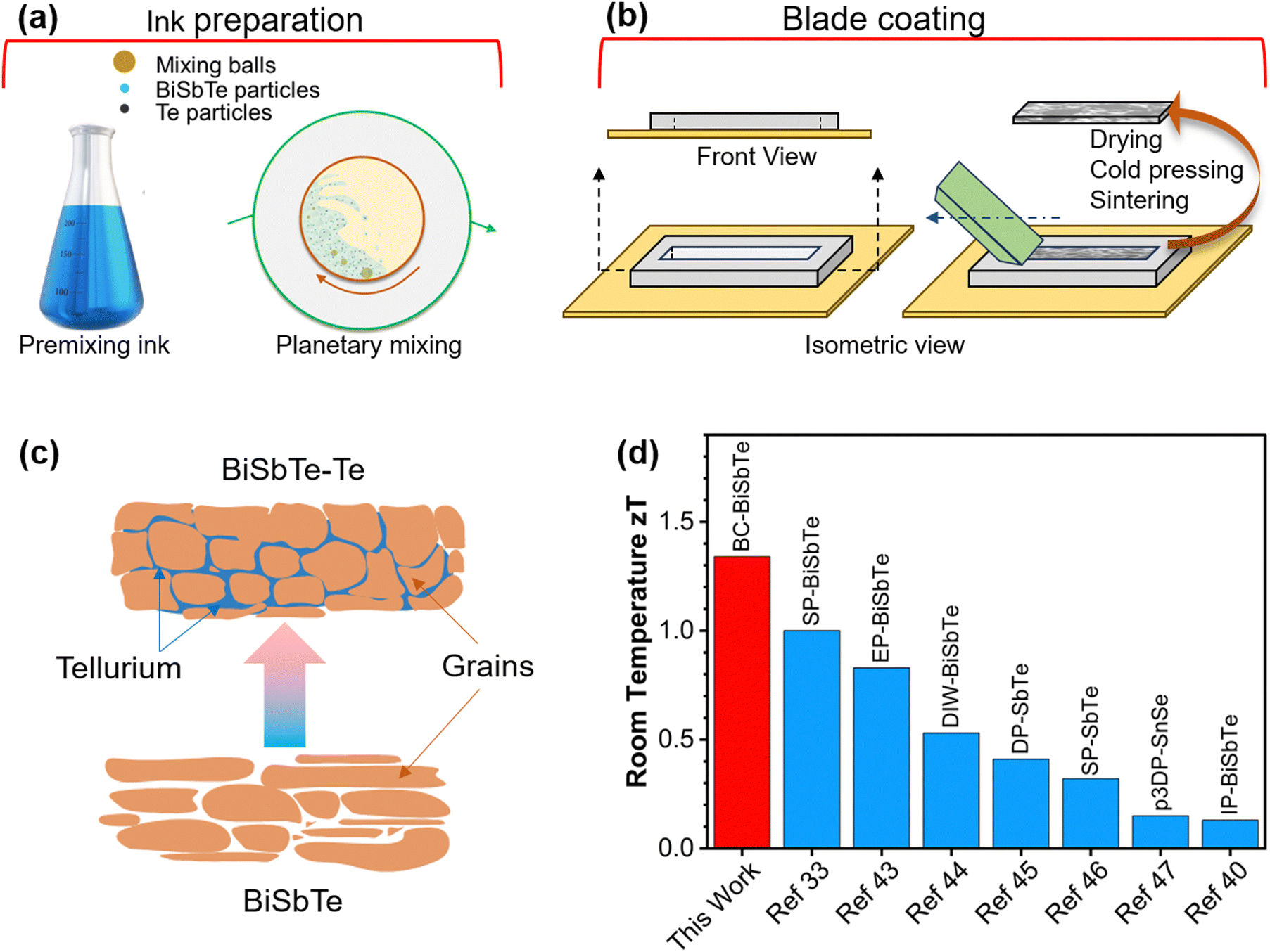 | ||
| Fig. 1 (a) Schematic representation of the thermoelectric ink formulation. (b) Blade coating for fabricating thick thermoelectric films. (c) Schematic of the Te-assisted liquid-phase sintering of BiSbTe. (d) Comparison of room-temperature zT between our blade-coated BiSbTe–Te sample and other p-type thermoelectric materials made with different ink-based processes33,40,43–47 (BC – blade coating, SP – screen printing, EP – extrusion printing, DIW – direct ink writing, DP – dispenser printing, p3DP – pseudo-3D printing, IP – inkjet printing). | ||
2. Results and discussion
2.1. Optimization of the ink formulation and sintering parameters
BiSbTe and its composites with excess Te were prepared using the blade-coating method. Thermoelectric material fabrication was completed in three steps: ink preparation, blade coating using a PDMS template, and post-processing of the coated thermoelectric films (Fig. 1(a) and (b)). The sample prepared by this innovative procedure is scalable to thick films and bulk pellets. The thermoelectric ink contains BiSbTe particles, Te particles, α-terpineol solvent, and Desperbyk-011 commercial binder. The rheology of the thermoelectric inks can be tuned by adjusting the ratio of the binder, solvent, and concentration of the thermoelectric powders (Fig. S2(a)–(f), ESI†). The binder enhances the particle surface interaction by acting as a binding agent. The frequency sweep result of the ink helped optimize the ink rheology for the blade coating by varying the binder percentage. The extensive changes in the storage and loss modulus (Fig. S1, ESI†) due to the binder addition provide effective control over the ink rheology to yield the most suitable ink for the blade coating process. As shown in Fig. S2(d)–(f) (ESI†), the power factor of the BiSbTe–Te sample peaked at the optimized binder addition of 16.7 wt%. The addition of Te significantly enhances the Seebeck coefficient of the sample (Fig. S2(a), ESI†) while decreasing the electrical conductivity, which results in a maximum room-temperature power factor of 3.44 mW m−1 K−2 at 8 wt% excess Te. The obtained power factor shows high reproducibility for 18 samples prepared in 7 batches in a span over a year (Table S1, ESI†). The post-processing included drying and cold pressing, followed by thermal sintering in a tube furnace that enhanced the density and electrical conductivity of the final structure. The cold pressing pressure, sintering time, and temperature were also optimized to maximize the power factor (Fig. S2(g)–(o), ESI†). The BiSbTe–Te sample with 8 wt% extra Te showed the highest power factor at an optimized sintering temperature of 450 °C for one hour using an ink containing 16.7 wt% binder. To confirm that the maximum power factor was obtained, we performed further optimization guided by BO with Gaussian process regression (GPR) as an ML surrogate model (Fig. S3(a), ESI†).48,49 The GPR model trained using the existing data with sintering parameters and ink variables as inputs and power factor as output showed reasonable accuracy (Fig. S3(b), ESI†). Fig. S3(c) (ESI†) shows that the model-predicted maximum is 3.37 mW m−1 K−2, which is within the uncertainty of the already achieved 3.44 mW m−1 K−2. Fig. S3(d) (ESI†) shows that the expected improvement (EI), an acquisition function balancing exploration and exploitation in BO, is low, with a maximum near the optimal conditions obtained above. Similarly, Fig. S4 (ESI†) shows the GPR predictions with confidence regions, which confirm that the final composition and sintering conditions are optimal. Therefore, while BO does not yield a higher power factor, it confirms that our optimization has already achieved the maximum power factor, and it provides quantitative guidance on when to terminate the experimental optimization while considering uncertainty.2.2. Crystallographic and microstructure analyses
We performed comprehensive analyses on both the baseline BiSbTe sample and the sample with an excess of 8 wt% Te (BiSbTe–Te) to understand the composition–structure–property relationship. X-ray diffraction (XRD) is performed at three different states, i.e. sintered films (Fig. 2(d)), pristine powder, crushed and powdered BiSbTe and BiSbTe–Te sintered film (Fig. S5, ESI†). All the peaks matched the Bi0.4Sb1.6Te3 crystal structure, with one additional peak found for elemental Te in BiSbTe–Te. Peak indexing for all peaks in the XRD pattern revealed major differences in the texture of the BiSbTe powder and sintered BiSbTe and BiSbTe–Te films. The pristine BiSbTe powder shows a relatively lower intensity of the 〈00l〉 peaks, unlike the sintered BiSbTe sample, denoting a reorientation and plate-like morphology after sintering. The 〈00l〉 peak intensity became less prominent, while a substantial increase in intensity was observed for other peaks for the BiSbTe–Te film, indicating a deviation from the plate-like morphology. To further understand this behavior, XRD was performed again after crushing the sintered films into a powder. All powdered samples showed a lower 〈00l〉 peak intensity, indicating reorientation of the BiSbTe's plate-like morphology with added Te in the BiSbTe–Te film. This texture difference can affect the transport properties of the materials as well.14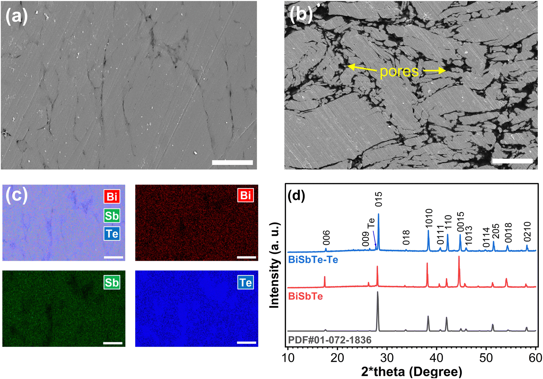 | ||
| Fig. 2 Scanning electron microscopy (SEM) images of the cross-section of (a) BiSbTe–Te (scale bar: 5 μm). (b) BiSbTe (scale bar: 5 μm) and (c) EDS elemental mapping of BiSbTe–Te (scale bar: 5 μm). (d) X-ray diffraction results of BiSbTe and BiSbTe–Te. The reference XRD curve at the bottom is for Bi0.4Sb1.6Te3 obtained from the ICSD (inorganic crystal structure database). | ||
SEM images of the polished cross-section (surface horizontal to the pressing direction) of the BiSbTe and BiSbTe–Te samples are shown in Fig. 2(a) and (b). BiSbTe–Te shows a denser microstructure than BiSbTe. Liquid-phase sintering, which is favored by the low melting point of Te enhances the densification of BiSbTe–Te. The more obvious 〈00l〉 orientation found in the XRD pattern of BiSbTe was present in the microstructure with aligned grains as stacked plates (Fig. 2(b) and Fig. S8(a), ESI†). For a more quantitative evaluation, image analysis measuring the aspect ratio of the fractured facets (Fig. S6(a) and (b), ESI†) showed a 48% higher ratio in BiSbTe–Te, which further validated the texture difference in XRD. EDS analysis of the BiSbTe–Te sample indicates that the excess Te is mostly distributed along the grain boundaries (Fig. 2(c) and Fig. S7, ESI†). In contrast, the BiSbTe sample did not show any Te distribution along its grain boundaries in the EDS elemental map (Fig. S8, ESI†). EDS analysis reveals a slightly higher Te concentration (63.6 at%) in BiSbTe–Te than the stoichiometric composition (60 at%) and the BiSbTe sample (57.9 at%). The excess Te detected by EDS could arise from Te at nearby grain boundaries, stacking faults, and dislocations in addition to point defects, typically Bi/Sb on Te antisite defects that produce holes as free charge carriers. The lower atomic ratio of Te compared to the stoichiometric composition (Bi0.4Sb1.6Te3) can be due to the evaporation of Te during the pressureless sintering.37 In general, Te deficiency indicates a Te-poor chemical potential that promotes the formation of acceptor defects (typically Bi/Sb on Te antisite defects), which is known to increase the hole concentration.50 Moreover, Te loss decreases the formation energy of antisite defects, which can cause higher hole concentration of antisites in BiSbTe and low Seebeck coefficient.13,51,52
2.3. Transport properties and zT
The temperature-dependent thermoelectric properties of the BiSbTe and BiSbTe–Te samples are shown in Fig. 3(a)–(c). The average carrier concentrations for BiSbTe and BiSbTe–Te were measured to be 6.5 × 1019 cm−3 and 7.3 × 1018 cm−3, respectively. The Te deficiency promotes the formation energy of antisite defects.50,52 The excess Te in the BiSbTe–Te sample results in Te-excess chemical potential and subsequently reduces the number of antisite defects, leading to reduced carrier concentration and enhanced Seebeck coefficient.14,33,53 The band gap calculated using the Goldsmid–Sharp equation is 0.20 eV, which is slightly higher than the reported values.29 The calculated effective mass (m*) from the Seebeck coefficient and carrier concentration for BiSbTe is 1.1me (me is the free electron mass), which is comparable to the literature reports.29,31,54 In the room-temperature Pisarenko plot, both BiSbTe and BiSbTe–Te samples could be well-fitted to 1.1me effective mass with a small deviation for BiSbTe–Te due to low carrier concentration (Fig. S10(b), ESI†).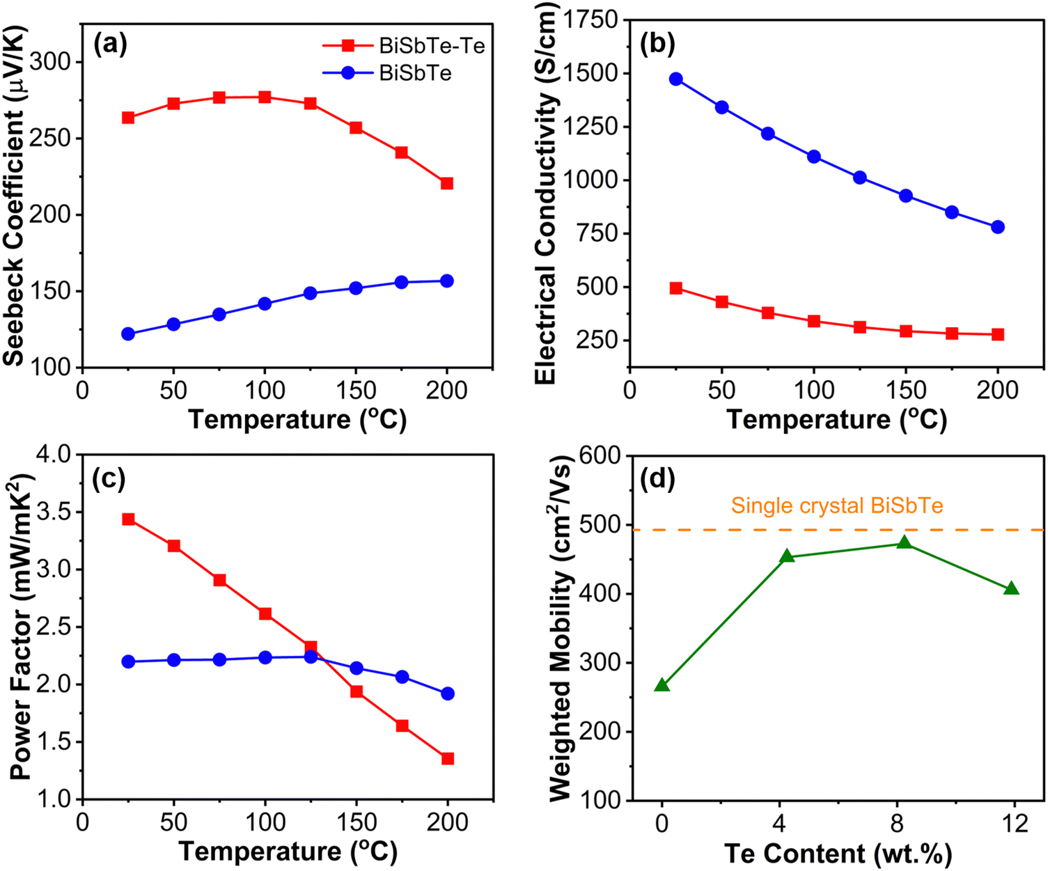 | ||
| Fig. 3 Temperature-dependent thermoelectric measurement results for (a) Seebeck coefficient, (b) electrical conductivity, (c) power factor. (d) Weighted mobility at varying Te concentrations. | ||
The temperature- and Te concentration-dependent weighted mobilities were calculated from the measured Seebeck coefficients and the electrical conductivities (Fig. 3(d) and Fig. S10(a) ESI†). The calculated weighted mobility (473 cm2 V−1 s−1) for BiSbTe–Te is very similar to the reported single-crystal value.13 Such high mobility ensures high electrical conductivity and Seebeck coefficient of BiSbTe–Te when the charge carrier concentration is optimized. The increased mobility of the Te excess sample is attributed to the reduced carrier scattering due to the diminished concentration of different types of defects (porosities and antisites).55 The high carrier concentration of BiSbTe leads to high conductivity despite the relatively low mobility. The electrical conductivity decreases with temperature for both BiSbTe and BiSbTe–Te samples, which is typical for heavily doped semiconductors. The significantly increased Seebeck coefficient and moderate electrical conductivity lead to an almost 75% increase in the power factor at room temperature for the BiSbTe–Te composite compared to the BiSbTe sample. The weighted mobility also decreases with temperature for both the samples (Fig. S10(a), ESI†) with a sharper slope of decrease for the BiSbTe–Te sample producing a lower power factor at high temperatures (Fig. 3(c)), which is typical of phonon-dominated scattering. The high thermoelectric performance of BiSbTe–Te showed repeatable performance with less than 5% variability between the subsequent temperature-dependent measurements (Fig. S9, ESI†).
To evaluate the zT of the samples, we measured the thermal diffusivity using the Angstrom method and calculated the thermal conductivity. The room-temperature thermal conductivities of BiSbTe–Te and BiSbTe are 0.77 and 1.18 W m−1 K−1, respectively. The reduced thermal conductivity, in combination with the increased power factor in BiSbTe–Te gives rise to a room temperature zT of 1.3, which is appreciably higher than that of other thermoelectric materials fabricated by ink-based methods (Fig. 1(d)). The electronic thermal conductivities of both samples can be calculated using the Wiedemann–Franz law, κe = LσT, where L is the Lorenz number calculated using the equation provided by Kim et al.56 The lattice thermal conductivity can be calculated as the difference between the total thermal conductivity and the electronic thermal conductivity (κl = κ − κe). The κl values of BiSbTe and BiSbTe–Te are 0.36 W m−1 K−1 and 0.53 W m−1 K−1 respectively, which are significantly lower than those of the bulk samples contributing to increased zT in BiSbTe–Te.35 The removal of solvent and binder during the drying and sintering processes coupled with the pressureless sintering results in the structures containing porosity, which leads to κl reductions compared with fully dense bulk compounds.57 The moderately increased κl in BiSbTe–Te can be attributed to the increased densification and possibly fewer defects with the addition of Te.
2.4. Device performance
To demonstrate the performance of the blade-coated BiSbTe–Te composite samples, an in-plane TEG device consisting of six BiSbTe–Te p-type legs connected by silver paint was fabricated. The contacts between the thermoelectric legs and electrodes were optimized by aerosol jet printing of a thin gold layer at the two ends of the BiSbTe–Te samples, followed by sintering in a furnace. The total device resistance measured was 7.35 Ω, which included the contact resistance (∼0.2 Ω per contact). The device performance was measured at the hot-side temperatures ranging from ∼40 °C to ∼140 °C, while the cold-side temperatures increased from 23 °C to 39 °C when the hot-side temperature increased. Finite element modeling using ANSYS was used to simulate the device performance using the experimentally measured thermoelectric properties as the input. The experimentally measured open-circuit voltages agree within 5% with the simulation results (Fig. 4(a)), which confirms the accuracy of the measured Seebeck coefficients. The device voltage–current characteristics and the output power shown in Fig. 4(b) and (c) also match the simulation results. With a temperature difference of 97.5 °C between the hot and cold sides, the output power and the power density are 0.84 mW and 27 mW cm−2, respectively (Fig. 4(d)), which is significantly higher than that of thermoelectric generators produced by ink-based methods.33,40,43,46,47 The maximum output power obtained is sufficient to power a wide range of low-power sensors and electronics.43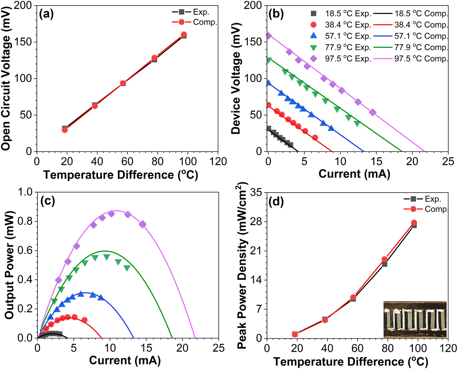 | ||
| Fig. 4 Thermoelectric device experimental (Exp.) and computational (Comp.) results as a function of various temperature differences between the hot and cold sides. (a) Open-circuit voltage vs. temperature difference. (b) Device voltage vs. current. (c) Output power vs. current. (d) Peak power density vs. temperature difference. The image of the device is shown in the inset. | ||
3. Conclusions
BiSbTe-based inks were formulated for the scalable processing of high-performance thermoelectric composites and devices. Excess Te-mediated liquid-phase sintering highly suppresses the defects in BiSbTe–Te to simultaneously increase the weighted mobility and Seebeck coefficient while reducing the carrier concentration and thermal conductivity, leading to a high zT of 1.3 at room temperature. The highly reproducible performance enables an in-plane thermoelectric device made of six legs of BiSbTe–Te, delivering a power density of 27 mW cm−2 at a temperature difference of 97.5 °C between the hot and cold sides. The scalable and low-cost processing technique reported in this work has the potential to transform thermoelectric device manufacturing and make thermoelectrics a commercially viable technology for energy harvesting and cooling applications.4. Materials and methods
4.1. Materials and ink preparation
Bismuth antimony telluride powder of 325 mesh size (99%) was obtained from Wuhan MCE Supply Co., Ltd. Tellurium (Te) powder (99.8%) of 200 mesh size, and the α-terpineol solvent (97%) were purchased from Sigma-Aldrich. The commercially available binder Disperbyk-011 was purchased from BYK. The ink solvent was prepared by adding α-terpineol and Desperbyk-011 at an appropriate ratio in a closed plastic container and stirring for six hours. Thermoelectric ink with 82 wt% solid loading for the blade coating of the thermoelectric film was prepared by mixing the thermoelectric particles and solvent in a sealed plastic container and mixing with a planetary mixer (AR-100) for one hour while stainless steel metal balls were added for thorough mixing. Ink rheology was tested using a Discovery HR-2 rheological testing machine before blade coating the thermoelectric films.4.2. Blade coating and post-processing
Cuboid-shaped (15 mm × 3 mm × 0.2 mm) thermoelectric samples were manufactured on a flexible polyimide substrate using a blade coating process. First, a polydimethylsiloxane (PDMS) template was prepared by casting. The template was then cleaned with isopropyl alcohol (IPA) and treated with oxygen plasma (Harrick Plasma Cleaner PDC-001-HP). PDMS was then attached to a plasma-cleaned polyimide substrate by hand pressing. An appropriate amount of thermoelectric ink was deposited into the PDMS template. Finally, a clean stainless-steel blade was run from one side to the other side of the template to ensure a homogeneous distribution of ink along the sample (Fig. 1(b)). After removing the template from the substrate, the ink assumes the cuboid shape of the PDMS template, thereby depositing a thermoelectric structure on the substrate. The two-step drying of the sample in air and forming gas (95% N2 and 5% H2) environment took place at 85 °C and 250 °C for 1 hour each. The dried samples are then cold-pressed at 25 MPa for 10 minutes in a hydraulic press for densification. The samples became freestanding and detached from the substrate after drying and cold pressing. The dried and cold-pressed samples were sintered without additional pressure in a tube furnace in a forming gas environment at varying temperatures and times to obtain the final thermoelectric structures.4.3. Thermoelectric and microstructural characterization
Temperature-based measurements of the Seebeck coefficient and electrical conductivity were performed using an in-house built setup. The setup consisted of two thermocouples for temperature measurements, two vertically aligned heaters for temperature control, and two electrodes for the current supply during the four probe electrical resistivity measurements. The thickness of the sample was measured using a Bruker DektakXT stylus profilometer using a 0.2 μm size stylus and 1 mg of force. A custom-built measurement setup based on the Angstrom method was used for the thermal diffusivity measurement.49 The details of the measurement procedure are provided in the ESI† (Fig. S11). Later, thermal conductivity was calculated based on the relationship κ = αρCp, where α is the thermal diffusivity, ρ is the mass density of the sample, and Cp is the constant pressure-specific heat capacity. The heat capacity was obtained from a previous publication.33 The Hall effect measurements were performed using a commercial HL5500PC system equipped with four probes. A Helios G4 UX Dual Beam microscope was used for microstructural characterization of the samples. EDS analysis was performed using a Bruker EDS equipped with an SEM. A detailed microstructural analysis was carried out by cross-sectioning and mirror polishing of the samples unless the grain boundaries were observed. X-ray diffraction patterns were collected using a Discover D8 X-ray diffraction machine.4.4. Thermoelectric device preparation, simulation, and measurement
A thermoelectric in-plane device was prepared by connecting six p-type BiSbTe–Te films in series (Fig. S12, ESI†). Only p-type legs were considered for the device to understand the performance improvement of only BiSbTe–Te. All samples were coated with a thin layer of gold particles at two longitudinal extremes to minimize contact resistance before being connected by silver paste. The gold layer was printed with an Optomec Aerosol Jet Printer, dried, and sintered in a furnace in a forming gas environment at 300 °C. Copper wires were used as electrodes in the thermoelectric devices. The thermoelectric device was tested in a setup with an electrical heater connected to the hot end of the device and a metal block with a hollow channel connected to the cold end. The hot- and cold-side temperatures were controlled by applying a voltage to the heater and a flowing stream of water to the metal block, respectively. The water flow rate was kept constant to maintain a constant cooling flux on the cold side. ANSYS Finite Element Analysis software was used to simulate the open-circuit voltage, current flow, electrical power output, and power density under a temperature differential between the cold and hot sides of the thermoelectric device. The temperature-dependent material properties of the Seebeck coefficient and resistivity were used as inputs for the thermoelectric multiphysics model. The electrical contact resistance between the device leg and electrode was measured using a four-wire measurement technique and was used as the input to the model.4.5. Machine learning
Bayesian optimization (BO) is a methodology widely applied in accelerating the discovery of functional materials.42 The traditional form of BO consists of Gaussian process regression (GPR) and expected improvement (EI).58 The EI metric predicts the value of additional experiments and is calculated using a GPR model with available experimental data. GPR emulates the behavior between manufacturing conditions (ink binder concentration, Te amount, sintering temperature, and sintering time) and the power factor, taking into account the inherent measurement errors within experiments and a kernel function to measure the similarity among manufacturing conditions. For our modeling, we employed Scikit-learn to develop the GPR model and optimized it using the lbfgs optimizer. Additionally, EI incorporates the trade-off between exploitation and exploration and is calculated based on GPR's predictive mean and uncertainty, helping experimentalists make informed decisions on future experiments. We developed a customized BO workflow for our framework and optimized the EI function using the lbfgs optimizer. The entire BO workflow, including modeling and recommendation, requires less than 3 minutes on a MacBook with a 2.6 GHz Intel Core i7 CPU.Author contributions
A. N. M. T. performed conceptualization, data curation, formal analysis, investigation, and writing – original draft. M. B. performed simulation, investigation, and writing – original draft. M. Z. performed conceptualization, methodology, and writing – review & editing. W. S., K. W., and K. S. performed methodology and investigation. Y. L. and E. I. performed validation. M. K. performed writing – review & editing. G. S. performed formal analysis, investigation, and writing – review & editing. A. D. and T. L. performed supervision and writing – review & editing. Y. Z. performed conceptualization, funding acquisition, project administration, supervision, and writing – review & editing.Conflicts of interest
The authors share no conflict of interest.Acknowledgements
We would like to acknowledge support from the U.S. Department of Energy under award DE-EE0009103. Y. Z. would like to acknowledge funding support from the National Science Foundation under award CMMI-1747685 and the U.S. Department of Energy under award DE-NE0009138. M. G. K. acknowledges support from the U.S. Department of Energy, Office of Science, and Office of Basic Energy Sciences under Award Number DE-SC0024256 (TE measurements and characterization). G. J. S. acknowledges support from the Office of Energy Efficiency and Renewable Energy (EERE) under the Advanced Manufacturing Office (AMO) award DE-EE0009104 (Northwestern University, TE measurements). K. W. also acknowledges ND Energy and the Patrick and Jana Eilers Graduate Student Fellowship for Energy-Related Research for providing financial support to advance this research.References
- M. Zeng, D. Zavanelli, J. Chen, M. Saeidi-Javash, Y. Du, S. LeBlanc, G. J. Snyder and Y. Zhang, Chem. Soc. Rev., 2022, 51, 485–512 RSC.
- G. Tan, L.-D. Zhao and M. G. Kanatzidis, Chem. Rev., 2016, 116, 12123–12149 CrossRef CAS PubMed.
- L. E. Bell, Science, 2008, 321, 1457–1461 CrossRef CAS PubMed.
- G. J. Snyder, S. LeBlanc, D. Crane, H. Pangborn, C. E. Forest, A. Rattner, L. Borgsmiller and S. Priya, Joule, 2021, 5, 748–751 CrossRef CAS.
- M. V. Vedernikov and E. K. Iordanishvili, in Seventeenth International Conference on Thermoelectrics. Proceedings ICT98 (Cat. No. 98TH8365), IEEE, Nagoya, Japan, 1998, pp. 37–42.
- G. J. Snyder and E. S. Toberer, Mater. Sustain. Energy A Collect. Peer-Reviewed Res. Rev. Artic. from Nat. Publ. Gr., 2010, 7, 101–110 Search PubMed.
- L. Wang, X. Zhang and L.-D. Zhao, Acc. Mater. Res., 2023, 4, 448–456 CrossRef CAS.
- Q. Yang, S. Yang, P. Qiu, L. Peng, T.-R. Wei, Z. Zhang, X. Shi and L. Chen, Science, 2022, 377, 854–858 CrossRef CAS PubMed.
- D. Liu, D. Wang, T. Hong, Z. Wang, Y. Wang, Y. Qin, L. Su, T. Yang, X. Gao, Z. Ge, B. Qin and L.-D. Zhao, Science, 2023, 380, 841–846 CrossRef CAS PubMed.
- S. Roychowdhury, T. Ghosh, R. Arora, M. Samanta, L. Xie, N. K. Singh, A. Soni, J. He, U. V. Waghmare and K. Biswas, Science, 2021, 371, 722–727 CrossRef CAS PubMed.
- H. Qin, Y. Zhang, S. Cai, Y. Sun, W. Wang, L. Xie, S. Sun, D. Qin, M. Guo, F. Guo, H. Wu, Q. Zhang, W. Cai and J. Sui, Chem. Eng. J., 2021, 425, 130670 CrossRef CAS.
- Y. Pan, U. Aydemir, J. A. Grovogui, I. T. Witting, R. Hanus, Y. Xu, J. Wu, C. F. Wu, F. H. Sun, H. L. Zhuang, J. F. Dong, J. F. Li, V. P. Dravid and G. J. Snyder, Adv. Mater., 2018, 30, 1–7 Search PubMed.
- L. Hu, T. Zhu, X. Liu and X. Zhao, Adv. Funct. Mater., 2014, 24, 5211–5218 CrossRef CAS.
- Y. M. Kim, R. Lydia, J. H. Kim, C. C. Lin, K. Ahn and J. S. Rhyee, Acta Mater., 2017, 135, 297–303 CrossRef CAS.
- Y. S. Wang, L. L. Huang, D. Li, J. Zhang and X. Y. Qin, J. Alloys Compd., 2018, 758, 72–77 CrossRef CAS.
- H.-L. Zhuang, H. Hu, J. Pei, B. Su, J.-W. Li, Y. Jiang, Z. Han and J.-F. Li, Energy Environ. Sci., 2022, 15, 2039–2048 RSC.
- N. S. Chauhan, S. V. Pyrlin, O. I. Lebedev, L. S. A. Marques, M. M. D. Ramos, T. Maiti, K. Kovnir, B. A. Korgel and Y. V. Kolen’Ko, J. Phys. Chem. C, 2021, 125, 20184–20194 CrossRef CAS.
- M. Burton, G. Howells, J. Atoyo and M. Carnie, Adv. Mater., 2022, 34, 2108183 CrossRef CAS PubMed.
- Q. Yan and M. G. Kanatzidis, Nat. Mater., 2022, 21, 503–513 CrossRef CAS PubMed.
- S. Choo, F. Ejaz, H. Ju, F. Kim, J. Lee, S. E. Yang, G. Kim, H. Kim, S. Jo, S. Baek, S. Cho, K. Kim, J.-Y. Kim, S. Ahn, H. G. Chae, B. Kwon and J. S. Son, Nat. Commun., 2021, 12, 3550 CrossRef CAS PubMed.
- M. R. Burton, S. Mehraban, D. Beynon, J. McGettrick, T. Watson, N. P. Lavery and M. J. Carnie, Adv. Energy Mater., 2019, 9, 1900201 CrossRef.
- J. Lee, S. Choo, H. Ju, J. Hong, S. E. Yang, F. Kim, D. H. Gu, J. Jang, G. Kim, S. Ahn, J. E. Lee, S. Y. Kim, H. G. Chae and J. S. Son, Adv. Energy Mater., 2021, 11, 2100190 CrossRef CAS.
- M. Zeng, H. Xie, M. Saeidi-Javash, A. Tanvir, Y. Du, J. Chen, M. G. Kanatzidis and Y. Zhang, J. Mater. Chem. A, 2021, 9, 22555–22562 RSC.
- M. Zeng, W. Kuang, I. Khan, D. Huang, Y. Du, M. Saeidi-Javash, L. Zhang, Z. Cheng, A. J. Hoffman and Y. Zhang, Adv. Mater., 2020, 32(39), 2003081 CrossRef CAS PubMed.
- M. Saeidi-Javash, W. Kuang, C. Dun and Y. Zhang, Adv. Funct. Mater., 2019, 29, 1901930 CrossRef.
- C. Dun, W. Kuang, N. Kempf, M. Saeidi-Javash, D. J. Singh and Y. Zhang, Adv. Sci., 2019, 6, 1901788 CrossRef CAS PubMed.
- Q. Zhu, S. Wang, X. Wang, A. Suwardi, M. H. Chua, X. Y. D. Soo and J. Xu, Nano-Micro Lett., 2021, 13, 119 CrossRef CAS PubMed.
- M. Zeng, Y. Du, Q. Jiang, N. Kempf, C. Wei, M. V. Bimrose, A. N. M. Tanvir, H. Xu, J. Chen, D. J. Kirsch, J. Martin, B. C. Wyatt, T. Hayashi, M. Saeidi-Javash, H. Sakaue, B. Anasori, L. Jin, M. D. McMurtrey and Y. Zhang, Nature, 2023, 617, 292–298 CrossRef CAS PubMed.
- I. T. Witting, T. C. Chasapis, F. Ricci, M. Peters, N. A. Heinz, G. Hautier and G. J. Snyder, Adv. Electron. Mater., 2019, 5, 1–20 Search PubMed.
- I. T. Witting, F. Ricci, T. C. Chasapis, G. Hautier and G. J. Snyder, Research, 2020, 2020, 4361703 CrossRef CAS PubMed.
- H. S. Kim, N. A. Heinz, Z. M. Gibbs, Y. Tang, S. D. Kang and G. J. Snyder, Mater. Today, 2017, 20, 452–459 CrossRef CAS.
- F. Kim, B. Kwon, Y. Eom, J. E. Lee, S. Park, S. Jo, S. H. Park, B.-S. Kim, H. J. Im, M. H. Lee, T. S. Min, K. T. Kim, H. G. Chae, W. P. King and J. S. Son, Nat. Energy, 2018, 3, 301–309 CrossRef CAS.
- T. Varghese, C. Dun, N. Kempf, M. Saeidi-Javash, C. Karthik, J. Richardson, C. Hollar, D. Estrada and Y. Zhang, Adv. Funct. Mater., 2020, 30, 1905796 CrossRef CAS.
- S. E. Yang, F. Kim, F. Ejaz, G. S. Lee, H. Ju, S. Choo, J. Lee, G. Kim, S. Ho Jung, S. Ahn, H. G. Chae, K. T. Kim, B. Kwon and J. S. Son, Nano Energy, 2021, 81, 105638 CrossRef CAS.
- S. Il Kim, K. H. Lee, H. A. Mun, H. S. Kim, S. W. Hwang, J. W. Roh, D. J. Yang, W. H. Shin, X. S. Li, Y. H. Lee, G. J. Snyder and S. W. Kim, Science, 2015, 348, 109–114 CrossRef PubMed.
- I. T. Witting, J. A. Grovogui, V. P. Dravid and G. J. Snyder, J. Mater., 2020, 6, 532–544 Search PubMed.
- H. Qin, W. Qu, Y. Zhang, Y. Zhang, Z. Liu, Q. Zhang, H. Wu, W. Cai and J. Sui, Adv. Sci., 2022, 9, 1–10 Search PubMed.
- Y. Tian and F. Molina-Lopez, Nanoscale, 2021, 13, 5202–5215 RSC.
- K. Jang, S. Yu, S. H. Park, H. S. Kim and H. Ahn, J. Alloys Compd., 2015, 618, 227–232 CrossRef CAS.
- B. Chen, M. Kruse, B. Xu, R. Tutika, W. Zheng, M. D. Bartlett, Y. Wu and J. C. Claussen, Nanoscale, 2019, 11, 5222–5230 RSC.
- B. Poudel, Q. Hao, Y. Ma, Y. Lan, A. Minnich, B. Yu, X. Yan, D. Wang, A. Muto, D. Vashaee, X. Chen, J. Liu, M. S. Dresselhaus, G. Chen and Z. Ren, Science, 2008, 320, 634–638 CrossRef CAS PubMed.
- K. Wang and A. W. Dowling, Curr. Opin. Chem. Eng., 2022, 36, 100728 CrossRef.
- F. Kim, S. E. Yang, H. Ju, S. Choo, J. Lee, G. Kim, S. Ho Jung, S. Kim, C. Cha, K. T. Kim, S. Ahn, H. G. Chae and J. S. Son, Nat. Electron., 2021, 4, 579–587 CrossRef CAS.
- Z. Wang, W. Cui, H. Yuan, X. Kang, Z. Zheng, W. Qiu, Q. Hu, J. Tang and X. Cui, Mater. Today Energy, 2023, 31, 101206 CrossRef CAS.
- D. Madan, A. Chen, P. K. Wright and J. W. Evans, J. Appl. Phys., 2011, 109, 2–7 CrossRef.
- S. J. Kim, J. H. We, J. S. Kim, G. S. Kim and B. J. Cho, J. Alloys Compd., 2014, 582, 177–180 CrossRef CAS.
- M. R. Burton, G. Howells, S. Mehraban, J. D. McGettrick, N. Lavery and M. J. Carnie, ACS Appl. Energy Mater., 2023, 6, 5498–5507 CrossRef CAS PubMed.
- W. Shang, M. Zeng, A. N. M. Tanvir, K. Wang, M. Saeidi-Javash, A. Dowling, T. Luo and Y. Zhang, Adv. Mater., 2023, 35, 2212230 CrossRef CAS PubMed.
- M. Saeidi-Javash, K. Wang, M. Zeng, T. Luo, A. W. Dowling and Y. Zhang, Energy Environ. Sci., 2022, 15, 5093–5104 RSC.
- S. Anand, M. Y. Toriyama, C. Wolverton, S. M. Haile and G. J. Snyder, Acc. Mater. Res., 2022, 3, 685–696 CrossRef CAS.
- Z. Starý, J. Horák, M. Stordeur and M. Stölzer, J. Phys. Chem. Solids, 1988, 49, 29–34 CrossRef.
- L. P. Hu, T. J. Zhu, Y. G. Wang, H. H. Xie, Z. J. Xu and X. B. Zhao, NPG Asia Mater., 2014, 6, 1–8 Search PubMed.
- R. J. Mehta, Y. Zhang, H. Zhu, D. S. Parker, M. Belley, D. J. Singh, R. Ramprasad, T. Borca-Tasciuc and G. Ramanath, Nano Lett., 2012, 12, 4523–4529 CrossRef CAS PubMed.
- G. J. Snyder, A. Pereyra and R. Gurunathan, Adv. Funct. Mater., 2022, 32, 1–6 CrossRef.
- S. Li, X. Fang, T. Lyu, J. Cheng, W. Ao, C. Zhang, F. Liu, J. Li and L. Hu, Mater. Today Phys., 2022, 27, 100764 CrossRef CAS.
- H.-S. Kim, Z. M. Gibbs, Y. Tang, H. Wang and G. J. Snyder, APL Mater., 2015, 3, 041506 CrossRef.
- Y. Zhang, R. J. Mehta, M. Belley, L. Han, G. Ramanath and T. Borca-Tasciuc, Appl. Phys. Lett., 2012, 100, 193113 CrossRef.
- B. Shahriari, K. Swersky, Z. Wang, R. P. Adams and N. de Freitas, Proc. IEEE, 2016, 104, 148–175 Search PubMed.
Footnote |
| † Electronic supplementary information (ESI) available. See DOI: https://doi.org/10.1039/d4ee00866a |
| This journal is © The Royal Society of Chemistry 2024 |