DOI:
10.1039/D1NR01600H
(Paper)
Nanoscale, 2021,
13, 8275-8282
High speed growth of MAPbBr3 single crystals via low-temperature inverting solubility: enhancement of mobility and trap density for photodetector applications†
Received
12th March 2021
, Accepted 6th April 2021
First published on 6th April 2021
Abstract
There has been growing interest in organic–inorganic hybrid perovskites as a promising candidate for optoelectronic applications due to their superior physical properties. Despite this, most of the reported perovskite devices based on polycrystalline thin films suffer immensely from poor stability and high trap density owing to grain boundaries limiting their performance. Perovskite single crystal structures have been recently explored to construct stable devices and reduce the trap density compared to their thin-film counterparts. We present a novel method of growing sizable CH3NH3PbBr3 single crystals based on the high solubility characteristic of hybrid perovskites at low temperatures within inverse temperature crystallization. We compared both the crystallinity of perovskite single crystal structures and optoelectronic charge transport of single crystal photodetectors as a function of dissolution temperature. The performance of the photodetector fabricated with our large-scaled single crystal with high quality demonstrated low trap density, high mobility, and high photoresponse.
Introduction
Hybrid metal halide perovskites MAPbX3 (MA = CH3NH3+, X = Cl−, Br−, or I−) have demonstrated high performance owing to their high absorption coefficient, direct bandgap, long carrier lifetime, high mobility, low cost, and facile deposition techniques,1–7 in optoelectronic applications for solar cells,1–3 light-emitting diodes,4,5 photodetectors6,7 and so on in the past few years. In addition to achieving the high performances of solar cells in a short period,1 the development of photodetectors has been driven by the beneficial optical and charge-transport properties of perovskites such as high photocurrent, responsivity, and response time.6 Rapid and great advances of perovskite polycrystalline film photodetectors have been achieved based on the development of the growth technique focusing on large-scale,6 low-cost solution-process and flexible applications.7 Beyond polycrystalline perovskite film photodetectors, there have recently been numerous structured perovskite devices such as single crystals8,9 or low dimensional structures.10,11 In particular, perovskite single crystals have recently shown superior properties such as longer carrier diffusion lengths, lower trap-state densities and better stability compared to their polycrystalline thin-film counterparts.8,9,12–23 However, reported perovskite single crystallization processes have some issues of extremely slow growth for large scale or unsatisfactory quality for demanding optoelectronic applications.15,21–24 Both fast growth and high quality large-scale perovskite single crystals enable a wide-spread utilization.
Numerous crystallization methods for perovskite single crystals have been introduced such as the conventional cooling technique, antisolvent vapor-assisted crystallization (AVC),13 top-seeded growth,14 liquid-diffused separation-induced crystallization,21 and inverse temperature crystallization (ITC).15,22,24–26 Bakr et al. reported the ITC method to grow high-quality large-scale perovskite single crystals fast, which is a widely used single crystal growth method. Crystallization is induced by reverse solubility dependent on the temperature of hybrid halide perovskites in specific solvents. Unlike the normal dissolution process, most perovskite molecules are bound in the complexes with the solvent, indicating dissolution. In addition, unbound molecules do not reach low-temperature saturation. The increase in temperature decreases the binding energy of the complexes. Therefore, unbound perovskite molecules increase and nucleation occurs when the solution supersaturates, followed by crystal growth.15,25 Although the precursor solution for the MAPbBr3 single crystal was prepared at room temperature,15,24 there seems to be room for the improvement of this technique considering the reverse solubility of MAPbBr3 for further high quality and large scale of single crystals.
In this study, an advanced ITC method is proposed by controlling the dissolution temperature. For the first time, the low-temperature inverting solubility of MAPbBr3 single crystals is demonstrated. We examined the effects of dissolution temperature on the MAPbBr3 quality and a single crystal device as a representative hybrid halide perovskite material. High quality and large-scale MAPbBr3 single crystals were fabricated with fast processing based on complete dissolution at low temperatures and fine heating control. The structural, optical, and electrical properties of single crystals grown at three dissolving temperatures were compared to investigate the essential parameters affecting the device performance. Furthermore, we demonstrated the potential to utilize a perovskite single crystal in practical optoelectrical application for observing the charge transport properties. The low temperature crystallization technique can be applied to numerous perovskite single crystal growth, which contributes to their high quality and large scale for the wide perovskite-based applications.
Results
In the solution-based perovskite single crystal growth, complete dissolution without residual molecules and growth temperature control are important factors in determining the quality of single crystals. Fig. 1 shows the low temperature inverting solubility with the dissolution mechanism depending on different temperatures, fine heating rate control and then the resulting CH3NH3PbBr3 (MAPbBr3) single crystals. The inverse temperature crystallization (ITC) method showed that the elevation of temperature leads to the crystallization of the precursor solution dissolved at low temperatures.15,25 This is related to the paradoxical solubility of the hybrid perovskite compound as opposed to a common monomolecular compound at high temperature.15,25,26 In Fig. 1a, as the advanced ITC technique, we devise the low temperature dissolution below 0 °C based on the measurement of low temperature inverting solubility for the first time, and the method of implementing them in detail is presented in Fig. S1.† According to the solubility and freezing temperature of the N,N-dimethylmethanamide (DMF) solvent (−61 °C), we dissolved a precursor solution at the low temperature (LT) of −40 °C, which was determined from the respective solubility of MAPbBr3. It consisted of the MAPbBr3-DMF complex under the more completely and clearly dissolved condition compared to the zero temperature (ZT) at 0 °C, and room temperature (RT) at 20 °C using undissolved precursors, as shown in Fig. 1a. Three different dissolution temperatures—RT, ZT, and LT—were kept in each bath using air, ice, and dry ice to compare the crystallization. Fig. 1b illustrates the heating rate of the crystallization in three different regions and the growing process at each temperature. In the ITC method, controlling the heating temperature was introduced to maintain constant temperature15 or extremely slow increase.24 Although crystallization with high quality is required over the longest possible time period theoretically, the reasonable adjustment of the process time should be necessary for commercial applications. Therefore, our gradient heating rate technique provides both the high quality and large size of single crystals for efficient time utilization within 6 h only. The heating rate was 0.5 °C min−1 between 20 °C and 60 °C, while it decreased gradually to 0.33 °C min−1 between 60 °C and 100 °C; furthermore, it decreased to 0.25 °C min−1 over 100 °C. Particularly, the period from 20 °C to 60 °C is the preparatory zone, where seed crystals are formed. The adaptation of the highest heating rate (0.5 °C min−1) on this zone leads to a significantly shorter time for the whole crystallization process compared to the results presented in previous literature.24 It demonstrated rapid crystal growth in low temperature period does not affect the realization of high quality according to our results of crystallization. Rather, the increase in the crystal size is prominently due to the increase in temperature in the high temperature period, as shown in Fig. S2,† which it can be seen synthetically that slow growth rate in high temperature region further helps to form the large crystal than controlling heating rate in low temperature region. In addition, although the heating temperature was controlled from 20 °C to 110 °C to the three different dissolution conditions equally, the temperature at which the seed crystal forms was different, corresponding to the point and arrow in Fig. 1b; at the lower dissolution temperature, the seed of single crystal was formed at a lower temperature as the starting point of the growth of single crystals. This also seems to potentially affect the final formation. Fig. 1c shows the largest MAPbBr3 single crystal at the lowest dissolution temperature with a parallelepiped shape. The size distribution of the crystal growth as the dissolution temperature was investigated via the repeated crystallization process, as shown in Fig. S3.† The relationship between the number of single crystals and crystal sizes shows that large-sized single crystals were distributed with the decrease in the dissolution temperature. In addition, the surface and cross-section images of single crystals via scanning electron microscopy (SEM) are shown in Fig. S4.† The image of single crystals in the LT condition was obtained only due to more deterioration of single crystals with ZT and RT conditions than that with the LT condition, which suggests the relationship between the quality and bonding of single crystals.
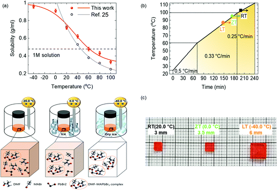 |
| | Fig. 1 (a) Temperature-dependent solubility of MAPbBr3 in DMF compared to ref. 21 and schematic diagram of dissolution temperature control, (b) heating rate of crystallization for high speed process, (c) MAPbBr3 single crystal size at different dissolution temperatures. | |
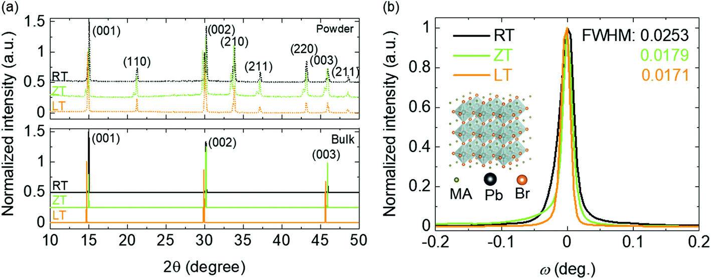
The X-ray diffraction (XRD) analysis of MAPbBr3 single crystals confirmed the crystalline quality, as shown in Fig. 2. Fig. 2a shows very sharp peaks in the XRD of powder single crystal, corresponding to the (001), (110), (002), (210), (211), (220), and (003) planes of the cubic MAPbBr3 crystal structure.24,27 Moreover, the maximal facet of MAPbBr3 single crystal XRD shows only (001), (002), and (003) peaks, indicating the superiority of a well-structured single crystal out of all single crystals with different dissolved temperatures.17,24 Furthermore, the first major XRD peaks were examined by high-resolution X-ray rocking curve analyses using full width at half maximum (FWHM) to compare the fine crystalline quality of three single crystals with different dissolved temperatures (see Fig. 2b). Single crystals in RT, ZT, and LT conditions showed 0.0253°, 0.0179°, and 0.0171° FWHM, respectively; it suggests that the quality of single crystals in the LT condition is the best than those with other dissolved temperatures. FWHM of our single crystal demonstrates the superior quality of crystallization in the LT condition than the other reference values of MAPbBr3 single crystals in the literatures.17,24,27 In addition, the single crystal X-ray diffraction of our MAPbBr3 single crystal confirmed that it had a cubic crystal structure and space group no. 221 (PmPm) with the lattice constant a = 5.907 Å, as shown in the inset of Fig. 2b, which is similar to the literature.15
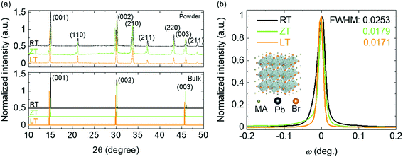 |
| | Fig. 2 X-ray diffraction of (a) powder and single crystal. (b) Rocking curve with different dissolution temperature. | |
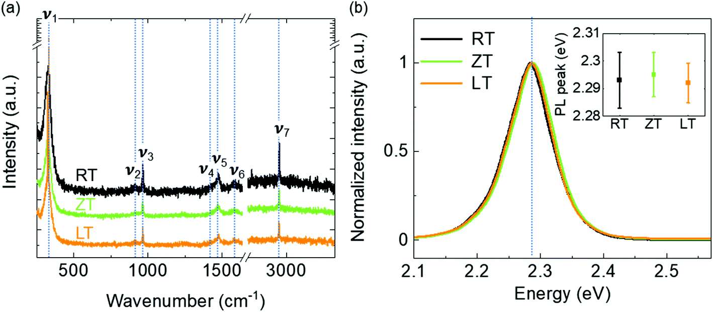
The optical and optoelectronic properties of three different single crystals were investigated, as shown in Fig. 3. Raman spectra of every single crystal confirmed MAPbBr3 crystal phases with a cubic structure.28,29 The vibration modes associated with organic atoms were observed above 200 cm−1, as listed in Table 1. The observed modes from three different samples were similar to those from the references and thus assigned accordingly.30,31 Specifically, the peak intensity of the ν1 (C–N torsion) mode was higher and the linewidth was narrower for a single crystal grown in the LT condition, which demonstrates that this crystal exhibits better crystalline quality than other crystals under RT and ZT conditions.32 The photoluminescence (PL) spectra exhibit one sharp peak at 2.29 eV (541 nm wavelength) for all the samples as is known in the literature.15 However, the difference of the PL peak at several measuring points of the sample is the smallest in the crystal in the LT condition, suggesting that uniformity of the LT sample is slightly better than other samples, as shown in the inset of Fig. 3b. In addition, the absorption of single crystal in the LT condition was investigated to be better than that of others, as shown in Fig. S5.†
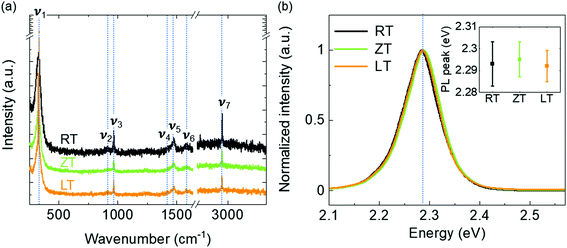 |
| | Fig. 3 (a) Raman and (b) PL spectra of MAPbBr3 single crystal with different dissolved temperatures. | |
Table 1 Raman shift of MAPbBr3 single crystals from the literature24,27
| Peaks (RT) |
Position (cm−1) |
Vibrational modes assignments (80 K) |
|
ν
1
|
327 |
C–N torsion |
τ (MA) |
|
ν
2
|
916 |
MA rocking |
ρ (MA) |
|
ν
3
|
970 |
C–N stretching |
ν (C–N) |
|
ν
4
|
1457 |
CH3 asymmetric bending |
δ
as(CH3) |
|
ν
5
|
1471 |
NH3 symmetric bending |
δ
s(NH3) |
|
ν
6
|
1589 |
NH3 asymmetric bending |
δ
as(NH3) |
|
ν
7
|
2957 |
CH3 asymmetric stretching |
ν
as(CH3) |
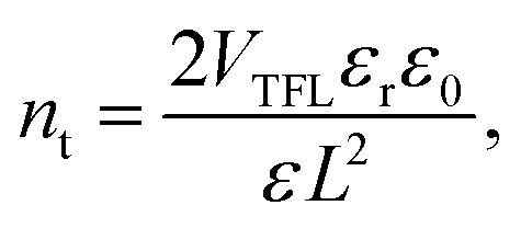
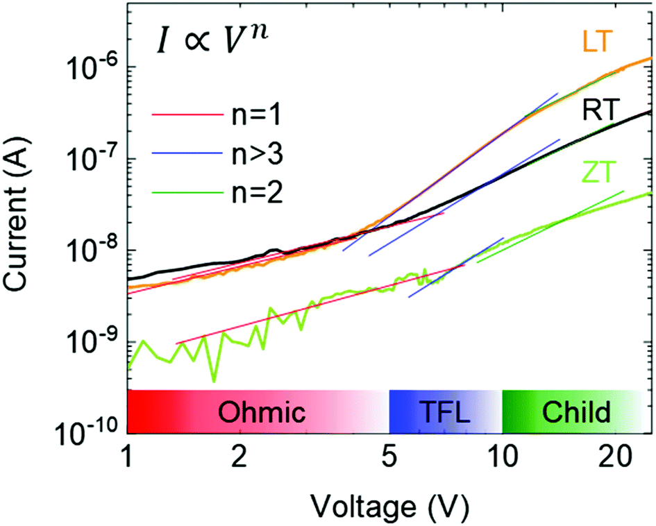
The carrier transport in dark was characterized by the space-charge-limited current (SCLC) method,33 as shown in Fig. 4. Although the mobility and carrier concentration of the semiconductor are accurately observed by the Hall effect measurement, the SCLC method was carried because the conductivity of our single crystals is within the measurement limit34,35 In particular, it shows the dark I–V properties of single crystals with different dissolved temperatures. The I–V curves are divided into three regions: ohmic (red line), trap-filling region (blue line), and trap free (green line). The trap density (ntrap) can then be determined by the trap-filled limit voltage, VTFL, the voltage at which the current begins to increase rapidly using following the equation:33,36
| |  | (1) |
where
ε0 is the vacuum permittivity,
εr is the relative dielectric constant (
εr = 25.5),
37e is the elementary charge (1.6 × 10
−19 C), and
L is the single-crystal thickness. The trap densities of a single crystal with different dissolved temperatures were determined according to the equation (see
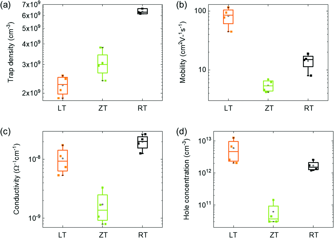
Table 2). It was found by comparing the trap densities that the performance of the single crystal device was the best in the LT condition. Moreover, within the reported trap density range of 26–200 × 10
9 cm
−3 for the MAPbBr
3 single crystals,
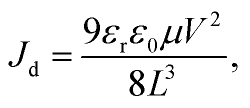
19 the ones produced in the LT condition are better than those produced under other dissolution temperature conditions. The carrier mobility over approximately 10 V of the single crystal was extracted by fitting the Mott–Gurney law:
15,38| | 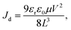 | (2) |
where
Jd is the dark current density,
μ is the mobility, and
V is the voltage. The mobility of the single crystal device in the LT condition was 115 cm
2 V
−1 s
−1, which is extremely larger than its microcrystalline thin-film counterpart
6 and the single crystals grown using ITC.
15,20 Moreover, the conductivity,
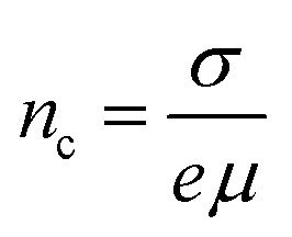
σ, of the ohmic region and hole concentration,
nc, are calculated using the following equation:
20| |  | (3) |
 |
| | Fig. 4 Dark I–V characteristics using SCLC method. | |
Table 2 Comparison of carrier transport
| Temperature |
Conductivity (Ω−1 cm−1) |
Trap density (cm−3) |
Mobility (cm2 V−1 s−1) |
Hole concentration (cm−3) |
| RT |
2.18 × 10⁻⁸ |
6.59 × 10⁹ |
18 |
2.55 × 10¹² |
| ZT |
3.31 × 10⁻⁹ |
3.06 × 10⁹ |
6 |
1.42 × 10¹¹ |
| LT |
1.53 × 10⁻⁸ |
2.55 × 10⁹ |
115 |
1.10 × 10¹³ |
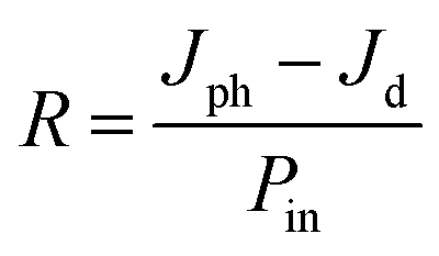
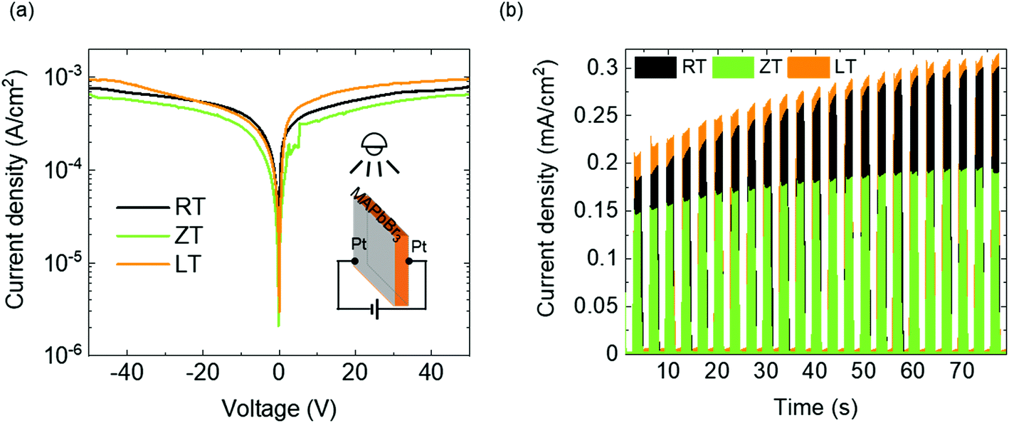
The values derived by fitting eqn (3) are listed in Table 2. The values indicate that the single crystal in the LT condition is superior in quality for photosensor applications than those MAPbBr3 single crystals grown using other techniques.15,20 The statistical results of these electrical measurements have supported the reliability of our technique for high-quality single crystal photodetectors (Fig. 5). The performance of photodetectors, such as photocurrent, responsivity and response time in single crystals, was investigated under white light with 5 mW cm−2. The I–V curves of the single-crystal device were measured, as shown in Fig. 6a. The photo current density was approximately 10−3 A cm−2, as expected from the high-quality single crystal.20 The high-quality photodetector fabricated in the LT condition shows the largest photo current density. Fig. 6b shows the time-dependent photoresponse of the single crystal device under white light and 2 V bias. In addition, the calculated responsivities, R of LT, ZT, RT samples are 0.059, 0.052, and 0.058 A W−1, respectively, using the following equation:
where
Jph is the photocurrent density and
Pin is the incident light power density.
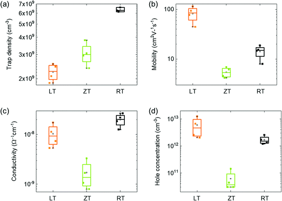 |
| | Fig. 5 (a) Trap density, (b) mobility, (c) conductivity, (d) hole concentration of MAPbBr3 single crystals with different dissolution condition. | |
 |
| | Fig. 6 (a) Photocurrent–voltage (I–V) curves of the photodetector and (b) on–off photoresponse at 2 V bias voltage under the white light. | |
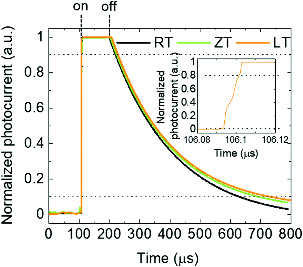
The responsivity of LT samples was slightly higher than that of others. In the measurement of response time shown in Fig. 7, a rapid increase in time (<20 ns) (the inset of Fig. 7) and slow decay time of single crystals can be observed. The decay times of LT, ZT, RT samples are 500, 470, 430 μs, respectively.
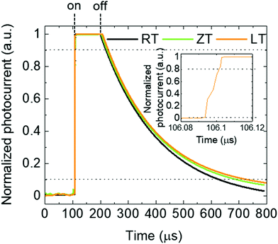 |
| | Fig. 7 Response times of MAPbBr3 single crystals with different dissolution conditions. | |
Numerous cycles of photocurrent density of this device indicate the reproducibility and stability of our single crystal photodetectors without any degradation. Table 3 shows the photoresponse characteristics of the reported MAPbBr3 single crystal photodetector, including the result of this work. Despite the active research on MAPbBr3 single crystals, its previous researches on photocurrent are rare and their performances are not high.20–23Fig. 6b surprisingly shows that not only did the LT state single crystal device exhibit the highest photocurrent density under all conditions, our results are the best among the previous literatures. Indeed, the increasing photocurrent depending on the illumination time is observed in Fig. 6b. One of causes for this behavior was suggested as the light trapping mediated by defect states, such as other optoelectronic devices.39 According to the recent research, the increasing photocurrent can be caused by the change of mobility.40 However, the mechanism study requires a detailed investigation of the carrier transport for perovskite materials, which is a subject of future research.
Table 3 Summary of the reported MAPbBr3 single crystal photodetectors
| Fabrication method |
Bias voltage (V) |
Light source |
Light intensity (mW cm−2) |
Photocurrent density (μA cm−2) |
Ref. |
| ITC |
2 |
White light |
5 |
314 |
This work |
| LDSC |
−4 |
White light |
— |
200 |
17
|
| ITC |
4 |
525 nm |
60 |
100 |
16
|
| ITC |
1.5 |
405 nm |
— |
25 |
18
|
| Mixed halide crystallization |
−4 |
White light |
0.4 |
0.04 |
19
|
Conclusion
We fabricated high quality MAPbBr3 single crystals and related optoelectronic devices with a low dissolution temperature (LT) based on the ITC method. Moreover, the low temperature inverting solubility was demonstrated in this study for the first time. The gradient heating rate led to a reduction in the growth processing time and high-quality large-scale single crystals. Improved crystalline quality in the LT condition, out of the three dissolved temperatures, was demonstrated owing to the narrow XRD rocking curve, high-intensity Raman peak, and spatial uniformity of PL peak. We show the potential of applying MAPbBr3 single crystals to the photodetector using a carrier transport in dark and illumination conditions. The SCLC analysis exhibited surprisingly low trap density and high mobility of single crystal devices formed in the LT condition. The photoresponse of the device was superior to the other two dissolution conditions as well as better than the reported results. This technology has great potential due to its scalability to various perovskite materials with inverse solubility and the simple and clear industrial application. Our novel growth technique with excellent optoelectronic properties of MAPbBr3 single crystals can contribute to manufacturing high-quality perovskite single crystals for the next generation optoelectronic devices.
Experimental method
Synthesis of MAPbBr3 single crystals
Methylammonium lead bromide (MAPbBr3) single crystals were grown based on the ITC method.15 Methylammonium bromide and lead bromide (PbBr2) were mixed with 1![[thin space (1/6-em)]](https://www.rsc.org/images/entities/char_2009.gif) :1 (PbBr2:MABr) in N,N-dimethylformamide (DMF) to prepare the growth solution. The temperature was set at three different values using ice and dry ice bath to dissolve the precursors. The solution was sonicated for 10 min for further dissolution and homogenization. Thereafter, it was filtered using a 0.2 μm PTFE filter. After filtration, the solution was divided among vials in 2 mL quantities and placed on the hotplate on a computational heating system. After growth, the crystals were dried in a vacuum chamber, as shown in Fig. S1.†
:1 (PbBr2:MABr) in N,N-dimethylformamide (DMF) to prepare the growth solution. The temperature was set at three different values using ice and dry ice bath to dissolve the precursors. The solution was sonicated for 10 min for further dissolution and homogenization. Thereafter, it was filtered using a 0.2 μm PTFE filter. After filtration, the solution was divided among vials in 2 mL quantities and placed on the hotplate on a computational heating system. After growth, the crystals were dried in a vacuum chamber, as shown in Fig. S1.†
Solubility test
2 ml of DMF in a vial was placed on a hot plate under stirring. Keeping the temperature, we started dissolving the amount of MABr and PbBr2 powder expected to be completely dissolved at the temperature in DMF. After checking the transparent solution, we added small amount of powder equivalent to 0.1 M. The same process was repeated at different temperatures. Temperatures of 0 and −40 °C have been investigated in the same method, but keeping the vial in an ice and dry ice bath.
Fabrication of the photodetector device
A photodetector was fabricated by depositing ≈100 nm Pt electrodes via vacuum sputtering on the single-crystalline perovskite MAPbBr3, which is the sandwich structure. On average, the sizes of the single crystal device in LT, ZT, RT condition are about 4 mm × 4 mm × 2 mm.
X-ray diffraction
X-ray diffraction (XRD) patterns of the MAPbBr3 powder and bulk of single crystal were recorded on an X-ray diffractometer (PANalytical, X'Pert Pro MPD) using a Cu-Kα (λ = 1.5418 Å) radiation source (40 kV, 30 mA).
Single crystal X-ray diffraction
The crystal structures of MAPbBr3 were ascertained by standard crystallographic methods. Orange block-shaped crystals were used for single-crystal X-ray diffraction. The data were collected at 223(2) K using a Bruker D8 Venture equipped with a IμS micro-focus sealed tube Mo Kα (λ = 0.71073 Å) and a PHOTON III M14 detector in Western Seoul Center of Korea Basic Science Institute. Data collection and integration were performed using the SMART APEX3 software package (SAINT+). Moreover, absorption correction was performed by the multi-scan method implemented in SADABS. The structure was solved by direct methods and refined by full-matrix least-squares on F2 using the SHELXTL program package (version 6.14).
Raman spectroscopy and photoluminescence
Raman scattering spectroscopy was performed to identify the phase formation of the material. All spectra were recorded using a McPherson 207 spectrometer equipped with a TE-cooled charge-coupled-device (CCD) array detector at room temperature. The samples were excited with 7.25 mW of a 632.8 nm He–Ne laser, focused to a ∼1 mm diameter spot using a microscope objective (100×). Room temperature photoluminescence (PL) spectra were recorded to characterize bandgap energies. We used 0.5 mW of a 488 nm diode laser as an excitation source.
Space charge limited current (SCLC) and photoresponse measurement
A photodetector was fabricated by depositing ≈100 nm Pt electrodes on both the sides of the perovskite MAPbBr3 single crystal via vacuum sputtering. The SCLC measurement was performed using a Keithley 2400 source-meter in dark at room temperature. The current–voltage (I–V) measurements were performed on a probe station connected to a Keithley 4200 semiconducting analyzer. The photoresponse was measured using white light having the intensity of 5 mW cm−2. The single normalized on/off cycle of the photocurrent was at a frequency of 30 Hz. The response time was measured by an Agilent Technologies DSO6054A oscilloscope with a 2 MΩ resistor.
Author contributions
Yunae Cho: Conceptualization, data curation, investigation, methodology, writing – original draft. Hye Ri Jung: Conceptualization, methodology. Yeon Soo Kim: Investigation. Yejin Kim: Investigation. Joohee Park: Investigation. Seokhyun Yoon: Validation, writing – review & editing. Yousil Lee: Methodology. Miyeon Cheon: Methodology, validation. Se-young Jeong: Methodology, validation. William Jo: Supervision, validation, writing – review and editing.
Conflicts of interest
There are no conflicts of interest to declare.
Acknowledgements
This research was supported by Basic Science Research Program through the National Research Foundation of Korea (NRF) funded by the Ministry of Education (NRF-2018R1A6A1A03025340, NRF-2016R1D1A1B01009032, and NRF-2020R1I1A1A01068700) and by the Ministry of Science, ICT & Future Planning (NRF-2017R1A2B3011822).
References
- N.-G. Park, Adv. Energy Mater., 2020, 10, 1903106 CrossRef CAS.
- S. Liu, Y. Guan, Y. Sheng, Y. Hu, Y. Rong, A. Mei and H. Han, Adv. Energy Mater., 2020, 10, 1902492 CrossRef CAS.
- M. Jung, S.-G. Ji, G. Kim and S. I. Seok, Chem. Soc. Rev., 2019, 48, 2011–2038 RSC.
- M. Lu, Y. Zhang, S. Wang, J. Guo, W. W. Yu and A. L. Rogach, Adv. Funct. Mater., 2019, 29, 1902008 CrossRef.
- S. D. Stranks, R. L. Z. Hoye, D. Di, R. H. Friend and F. Deschler, Adv. Mater., 2019, 31, 1803336 CrossRef CAS PubMed.
- J. Miao and F. Zhang, J. Mater. Chem. C, 2019, 7, 1741–1791 RSC.
- D. Hao, J. Zou and J. Huang, InfoMat, 2020, 2, 139–169 CrossRef CAS.
- Q. Dai, X. Chen, R. Ding, Y. Peng, W. Lv, Z. Zhou, S. Xu and L. Sun, Opt. Mater., 2021, 111, 110684 CrossRef CAS.
- K. Wang, L. Jing, Q. Yao, J. Zhang, X. Cheng, Y. Yuan, C. Shang, J. Ding, T. Zhou, H. Sun, W. Zhang and H. Li, J. Phys. Chem. Lett., 2021, 12, 1904–1910 CrossRef CAS PubMed.
- S. Wang, Y. Chen, J. Yao, G. Zhao, L. Li and G. Zou, J. Mater. Chem. C, 2021 10.1039/D1TC00408E.
- H.-P. Wang, S. Li, X. Liu, Z. Shi, X. Fang and J.-H. He, Adv. Mater., 2021, 33, 2003309 CrossRef CAS PubMed.
- X. D. Wang, W. G. Li, J. F. Liao and D. B. Kuang, Sol. RRL, 2019, 3, 1800294 CrossRef.
- D. Shi, V. Adinolfi, R. Comin, M. Yuan, E. Alarousu, A. Buin, Y. Chen, S. Hoogland, A. Rothenberger, K. Katsiev, Y. Losovyj, X. Zhang, P. A. Dowben, O. F. Mohammed, E. H. Sargent and O. M. Bakr, Science, 2015, 347, 519–522 CrossRef CAS PubMed.
- Q. Dong, Y. Fang, Y. Shao, P. Mulligan, J. Qiu, L. Cao and J. Huang, Science, 2015, 347, 967–970 CrossRef CAS PubMed.
- M. I. Saidaminov, A. L. Abdelhady, B. Murali, E. Alarousu, V. M. Burlakov, W. Peng, I. Dursun, L. Wang, Y. He, G. Maculan, A. Goriely, T. Wu, O. F. Mohammed and O. M. Bakr, Nat. Commun., 2015, 6, 7586 CrossRef PubMed.
- X. Jiang, X. Fu, D. Ju, S. Yang, Z. Chen and X. Tao, ACS Energy Lett., 2020, 5, 1797–1803 CrossRef CAS.
- W. Peng, L. Wang, B. Murali, K.-T. Ho, A. Bera, N. Cho, C.-F. Kang, V. M. Burlakov, J. Pan, L. Sinatra, C. Ma, W. Xu, D. Shi, E. Alarousu, A. Goriely, J.-H. He, O. F. Mohammed, T. Wu and O. M. Bakr, Adv. Mater., 2016, 28, 3383–3390 CrossRef CAS PubMed.
- J. Huang, Y. Shao and Q. Dong, J. Phys. Chem. Lett., 2015, 6, 3218–3227 CrossRef CAS.
- H.-S. Rao, W.-G. Li, B.-X. Chen, D.-B. Kuang and C.-Y. Su, Adv. Mater., 2017, 29, 1602639 CrossRef PubMed.
- Y. Liu, Y. Zhang, K. Zhao, Z. Yang, J. Feng, X. Zhang, K. Wang, L. Meng, H. Ye, M. Liu and S. Liu, Adv. Mater., 2018, 30, 1707314 CrossRef PubMed.
- F. Yao, J. Peng, R. Li, W. Li, P. Gui, B. Li, C. Liu, C. Tao, Q. Lin and G. Fang, Nat. Commun., 2020, 11, 1194 CrossRef CAS PubMed.
- H.-H. Fang, S. Adjokatse, H. Wei, J. Yang, G. R. Blake, J. Huang, J. Even and M. A. Loi, Sci. Adv., 2016, 2, e1600534 CrossRef PubMed.
- Y. Fang, Q. Dong, Y. Shao, Y. Yuan and J. Huang, Nat. Photonics, 2015, 9, 679–686 CrossRef CAS.
- Y. Liu, Y. Zhang, Z. Yang, J. Feng, Z. Xu, Q. Li, M. Hu, H. Ye, X. Zhang, M. Liu, K. Zhao and S. Liu, Mater. Today, 2019, 22, 67–75 CrossRef CAS.
- M. I. Saidaminov, A. L. Abdelhady, G. Maculan and O. M. Bakr, Chem. Commun., 2015, 51, 17658–17661 RSC.
- G. Maculan, A. D. Sheikh, A. L. Abdelhady, M. I. Saidaminov, M. A. Haque, B. Murali, E. Alarousu, O. F. Mohammed, T. Wu and O. M. Bakr, J. Phys. Chem. Lett., 2015, 6, 3781–3786 CrossRef CAS PubMed.
- J. T. Tisdale, T. Smith, J. R. Salasin, M. Ahmadi, N. Johnson, A. V. Ievlev, M. Koehler, C. J. Rawn, E. Lukosi and B. Hu, CrystEngComm, 2018, 20, 7818–7825 RSC.
- L. C. Schmidt, A. Pertegás, S. González-Carrero, O. Malinkiewicz, S. Agouram, G. M. Espallargas, H. J. Bolink, R. E. Galian and J. Pérez-Prieto, J. Am. Chem. Soc., 2014, 136, 850–853 CrossRef CAS PubMed.
- H. R. Jung, G. Y. Kim, B. P. Nguyen, H.-J. Jin, W. Jo, T. T. T. Nguyen, S. Yoon, W. S. Woo, C. W. Ahn, S. Cho and I. W. Kim, J. Phys. Chem. Lett., 2017, 121, 21930–21934 CrossRef CAS.
- L.-Q. Xie, T.-Y. Zhang, L. Chen, N. Guo, Y. Wang, G.-K. Liu, J.-R. Wang, J.-Z. Zhou, J.-W. Yan, Y.-X. Zhao, B.-W. Mao and Z.-Q. Tian, Phys. Chem. Chem. Phys., 2016, 18, 18112–18118 RSC.
- T. Zhang, L. Xie, L. Chen, N. Guo, G. Li, Z. Tian, B. Mao and Y. Zhao, Adv. Funct. Mater., 2017, 27, 1603568 CrossRef.
- M. R. Joya, K. M. Fonseca and J. Barba-Ortega, AIP Conf. Proc., 2014, 1627, 42–45 CrossRef CAS.
- R. H. Bube, J. Appl. Phys., 1962, 33, 1733–1737 CrossRef CAS.
- O. S. Mortensen, R. W. Munn and D. F. Williams, J. Appl. Phys., 1971, 42, 1192–1203 CrossRef.
- T. Yamasaki, K. Ueno, A. Tsukazaki, T. Fukumura and M. Kawasaki, Appl. Phys. Lett., 2011, 98, 082116 CrossRef.
- P. Mark and W. Helfrich, J. Appl. Phys., 1962, 33, 205–215 CrossRef CAS.
- A. Poglitsch and D. Weber, J. Chem. Phys., 1987, 87, 6373–6378 CrossRef CAS.
- J. Xing, Y. Zou, C. Zhao, Z. Yu, Y. Shan, W. Kong, X. Zheng, X. Li, W. Yu and C. Guo, Mater. Today Phys., 2020, 14, 100240 CrossRef.
- Y. Cho, J. Hwang, I. Jeong, J. Gwak, J. H. Yun, K. Kim and W. Jo, Sol. Energy Mater. Sol. Cells, 2021, 220, 110860 CrossRef CAS.
- C. L. Watts, L. Aspitarte, Y.-H. Lin, W. Li, R. Elzein, R. Addou, M. J. Hong, G. S. Herman, H. J. Snaith and J. G. Labram, Commun. Phys., 2020, 3, 73 CrossRef CAS.
Footnote |
| † Electronic supplementary information (ESI) available. See DOI: 10.1039/d1nr01600h |
|
| This journal is © The Royal Society of Chemistry 2021 |
Click here to see how this site uses Cookies. View our privacy policy here. 
 a,
Hye Ri
Jung
a,
Yeon Soo
Kim
a,
Yejin
Kim
a,
Joohee
Park
a,
Seokhyun
Yoon
a,
Hye Ri
Jung
a,
Yeon Soo
Kim
a,
Yejin
Kim
a,
Joohee
Park
a,
Seokhyun
Yoon