
 Open Access Article
 This Open Access Article is licensed under a
 Creative Commons Attribution 3.0 Unported Licence
Revisiting anodic alumina templates: from fabrication to applications
Alejandra
Ruiz-Clavijo
 ,
Olga
Caballero-Calero
* and
Marisol
Martín-González
,
Olga
Caballero-Calero
* and
Marisol
Martín-González
Instituto de Micro y Nanotecnología, IMN-CNM, CSIC (CEI UAM+CSIC) Isaac Newton, 8, E-28760, Tres Cantos, Madrid, Spain. E-mail: olga.caballero@csic.es
First published on 7th January 2021
Abstract
Anodic porous alumina, –AAO– (also known as nanoporous alumina, nanohole alumina arrays, –NAA– or nanoporous anodized alumina platforms, –NAAP–) has opened new opportunities in a wide range of fields, and is used as an advanced photonic structure for applications in structural coloration and advanced optical biosensing based on the ordered nanoporous structure obtained and as a template to grow nanowires or nanotubes of different materials giving rise to metamaterials with tailored properties. Therefore, understanding the structure of nanoporous anodic alumina templates and knowing how they are fabricated provide a tool for the further design of structures based on them, such as 3D nanoporous structures developed recently. In this work, we review the latest developments related to nanoporous alumina, which is currently a very active field, to provide a solid and thorough reference for all interested experts, both in academia and industry, on these nanostructured and highly useful structures. We present an overview of theories on the formation of pores and self-ordering in alumina, paying special attention to those presented in recent years, and different nanostructures that have been developed recently. Therefore, a wide variety of architectures, ranging from ordered nanoporous structures to diameter changing pores, branched pores, and 3D nanostructures will be discussed. Next, some of the most relevant results using different nanostructured morphologies as templates for the growth of different materials with novel properties and reduced dimensionality in magnetism, thermoelectricity, etc. will be summarised, showing how these structures have influenced the state of the art in a wide variety of fields. Finally, a review on how these anodic aluminium membranes are used as platforms for different applications combined with optical techniques, together with principles behind these applications will be presented, in addition to a hint on the future applications of these versatile nanomaterials. In summary, this review is focused on the most recent developments, without neglecting the basis and older studies that have led the way to these findings. Thus, it gives an updated state-of-the-art review that should be useful not only for experts in the field, but also for non-specialists, helping them to gain a broad understanding of the importance of anodic porous alumina, and most probably, endow them with new ideas for its use in fields of interest or even developing the anodization technique.
1 Introduction
Porous anodic aluminium oxide (AAO) membranes are a hot research topic due to their great versatility with applications in a wide range of scientific fields. AAO membranes provide a cost-effective platform to obtain structures with a high density of ordered pores with diameters in the order of nanometers and with lengths that can reach the micrometer range. Since the published work by Masuda et al. in 1990,1 where the fabrication process of highly ordered porous structured alumina membranes in oxalic acid was first reported, research has come a long way. New conditions under different anodization regimens have been discovered in many different types of acidic electrolytes and experimental conditions (temperature, applied anodization potential, etc.),2–13 which allow alumina membranes with pre-designed porous structures (pore diameter, inter-pore distance, porosity, length, etc.) to be obtained for certain applications. This high degree of tunability of the porous structure at the nanoscale level allows a fine control of the optical properties displayed by alumina films, which can be exploited for sensing applications.14–20 Furthermore, their high surface to volume ratio (associated with their pore density) makes them appropriate vehicles for drug delivery applications.21–25 These membranes can be further used as templates for micro- and nano-structuration of different materials, which is highly demanded in the nanotechnology field. Several distinct morphologies ranging from solid nanowires,26–35 segmented nanowires of varying compositions36–38 or diameters,37,39 hollow tubular wires, also referred to as nanotubes,40–48 nanocones,49 and Y-branched wires50–56 to 3D networks of interconnected nanowires26,57–62 can be obtained by filling the previously generated porous structure. This can be achieved through different growth techniques such as electrochemical deposition (ED), Chemical Vapour Deposition (CVD), Atomic Layer Deposition (ALD), and sputtering, among others. Holey films,63–68 also known as antidot arrays, can be fabricated if the deposition of a certain material takes place only over the surface of a hollowed membrane, replicating this structure. Depending on the chosen material, different phenomena and interesting optical, electric, and magnetic properties have been observed in the above mentioned shapes. Hence, alumina membranes provide powerful platforms for studying the property changes occurring at the nanoscale.Nowadays, there is a wide variety of materials and fabrication techniques that can produce nanostructures or highly nanoporous media for their use in different applications. For instance, for the fabrication of hard templates with features at the nanoscale, there are several possibilities.69,70 One type of widely used nanostructured 3D templates is opals or inverse opals, where the final structure depends on the dimensions of the starting spheres (ranging from 140 to 350 nm, approx.) and their nature (polystyrene, silica, etc.). Also, one can consider lithography-based techniques, such as two-photon lithography, which can produce 3D templates. In this case, very exotic structures can be designed, but this is a costly and time-consuming technique, and the typical dimensions of the obtained features are hundreds of nanometers in diameter.71 Another way to obtain nanopore templates is the fabrication of ion-track-etched polymeric membranes, where a high density of parallel pores with diameters in the range of tens to hundreds of nanometers and microns in length can be obtained. Even 3D structures based on irradiating polymeric membranes with different incident angles to their surface can be achieved. Nevertheless, in this case, the drawbacks are that there is no ordering of the nanopores or control over their actual position, and an ion accelerator is needed to produce the tracks.72 Other types of widely used nanoporous structures in current research, besides AAOs, are porous polymers, such as block copolymers73 and metal-organic frameworks (MOFs),74 which provide a high surface to volume ratio, but they also have limited thermal stability, where none of them able to function over 600 °C,75 and limited thickness of the achieved nanostructures. Also, the research on mesoporous silica76 is relevant, but in this case, mostly silica nanoparticles (100 to 500 nm in diameter) with a porous surface (ranging from 2 to 50 nm in diameter) are employed, which give rise to different architectures than that obtained with AAOs. Then, as we will see through this review, AAOs appear as the most suitable platforms for a great number of applications, either as porous materials themselves or templates for the fabrication of a variety of nanostructured architectures. They provide thermal stability to the structures, even over 1000 °C,77 large areas of high density pores, good control over the pore diameter (which can range from tens to hundreds of nm), great control over the structural parameters of 3D structures, and a large aspect ratio with a cost-effective, easily scalable method, and therefore, are widely used and provide an active field of research.
In this work, an updated review of the state of the art of this rapidly evolving field is presented, starting with a description of the AAO porous structure and the most used parameters for its fabrication (section 2). Then, the different theories for the mechanisms of pore formation are discussed (section 3), followed by an insight into the two most used anodization regimes, namely mild and hard anodization (section 4). Once the theory and most used regimes are introduced, the influence of the anodization conditions to obtain different morphologies of porous structures, such as branched structures, pores with modulated diameters, and even 3D porous structures, is reviewed (section 5). The last part of this manuscript is devoted to a review of the latest publications on the applications of the different AAO porous structures, both as templates to grow replicas of their nanoporous structures in different materials (section 6) and due to their nanoporous structure themselves (section 7), which make them ideal candidates for applications such as structural coloration, photonic structures, and sensors. Accordingly, this work aims to provide a deep understanding of AAO nanoporous structures, from their formation mechanisms to their technological applications.
2 AAO porous structure
The electrochemical oxidation of a metal, also known as anodization, is a simple and low-cost electrochemical process that produces an oxide layer on the target metallic surface over large areas. This process has been used to obtain nanoporous, nanotubular, and other types of nanostructured functional oxide layers on a wide variety of metals and semimetals, such as gold,78 cobalt,79 copper,80 gallium,81 hafnium,82 iron,83 molybdenum,84 niobium,85 tin,86 titanium,87,88 tungsten,89 vanadium,90 zinc,91 and zirconia.92 These oxide films have many applications in catalysis,78,79,84 photocatalysis,83,87,89,91 supercapacitors,90 photoelectrodes,88 thermal protection,92etc. In most cases, the applications take advantage of the large surface to volume ratio of the formed structures. In the case of aluminium anodization, it was intensively studied firstly for the protection of surfaces, and recently, most of the research has been devoted to the fabrication of nano-devices and ordered tunable nanostructures. Anodic aluminium oxide (AAO) is also produced via the electrochemical oxidation of an aluminium substrate, which is usually performed in a two-electrode electrochemical cell, where the working electrode is aluminium. Depending on the electrolyte composition, two different types of anodic oxides can be grown, compact non-porous anodic aluminium oxide and porous alumina films.To better understand the formation process of this nanoporous structure, one first has to understand how a simpler structure, namely non-porous anodic aluminium oxide films, is produced. In this case, solutions with pH 5–7, in which the anodic aluminium oxide is insoluble, are used. Then, under a certain applied voltage, an insulator oxide barrier layer is formed. In brief, the process involves the migration of oxygen-containing ions (O2− and OH−) into the metal from the metal-oxide interface, while the metal ions can either form an oxide layer or be released to the electrolyte. The current density flowing through this barrier layer eventually decays due to its insulating behavior, limiting the maximum thickness of the resulting barrier oxide layer. Therefore, the final thickness of this non-porous alumina is proportional to the anodization potential (U). These films are usually used for corrosion protection.
Nanoporous AAO membranes are obtained in a more acidic medium to slightly increase the solubility of the anodic oxide barrier layer. In this case, the abovementioned nonporous barrier layer is also formed when a certain potential is applied, but then, due to the increased solubility of this layer in an acidic environment, a porous anodic oxide layer starts to grow. In this system, the thickness of the barrier layer remains constant throughout the process due to the balanced competition between the new anodic oxide formed and the oxide dissolution at the oxide/electrolyte interface.93 This process will be described in detail in section 3, where the formation and growth mechanisms will be discussed. Here, simply, the final thickness of the porous AAO membrane is directly proportional to the anodization time.
Then, by controlling the anodization conditions (temperature, anodization voltage, anodization time, electrolyte composition, etc.), self-ordering of the vertical pores in a closed-packed hexagonal pattern can be achieved (Fig. 1). Under the conditions that give rise to self-ordering of the pores, each pore forms a hexagonal unit cell. The most characteristic parameters of the porous structure are the pore diameter (Dp), interpore distance, (Dint), which also refers to the cell size, and barrier layer thickness (tb).
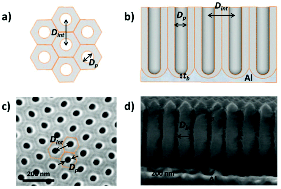 | ||
| Fig. 1 (a) Schematic top view of the arrangement of 6 hexagonal pore unit cells. (b) Lateral sketch view of an anodic oxide aluminium porous membrane. (c) Top and (d) cross-sectional view SEM images of a lab-made alumina membrane (0.3 M oxalic acid). Structural parameters of the alumina porous structure including pore diameter (Dp), interpore distance, (Dint), and barrier layer thickness (tb) are identified in all the images. | ||
Depending on the temperature, electrolyte composition, and applied potential, the structural parameters of the porous structure of alumina membranes can be varied, mainly the pore diameter, interpore distance, and barrier layer thickness. Similar to non-porous anodic oxide films, the thickness of the barrier layer is proportional to the anodization potential (U). S. Z. Chu et al. studied the linear relationship between U and tb in different acidic media,94 (see Fig. 2). However, there is no unified explanation for how each of the abovementioned electrochemical factors influences the diameter pore and interpore distance. In general, it is accepted that the anodizing potential (or current density) increases the pore diameter95 and interpore distance95–97 according to the following expressions under mild anodization conditions (see section 4.1).
| Dp = ξp × U = 1.29 × U | (1) |
| Dint = ξMA × U = 2.5 × U | (2) |
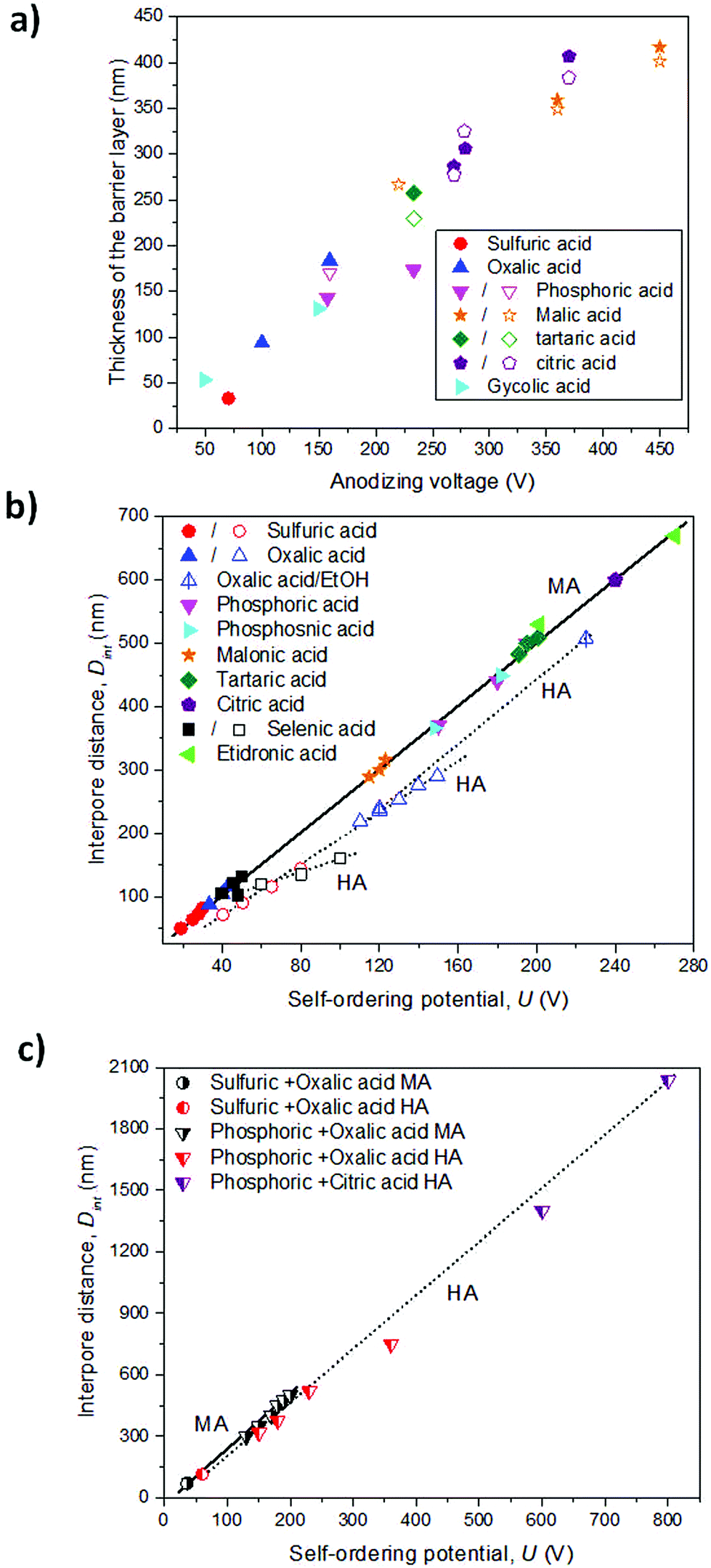 | ||
| Fig. 2 (a) Evolution of the thickness of the barrier layer as a function of the anodizing potential in different acidic electrolytes.94 Solid symbols represent the measured values. Open symbols, calculated values from the half-thickness of the pore wall. (b) Self-ordering regimes under MA (solid symbols) and HA (open symbols) in different electrolytes. (c) Self-ordering conditions of mixed electrolytes, under MA (black symbols) and HA (red and purple symbols) regimes. The black solid line and black dotted lines were added to guide the eye, showing the linear correlation of the cell size (or interpore distance, Dint) and the anodizing potential (U) under MA and HA conditions, respectively. Data was taken from Table 1. | ||
where Dp and Dint are the pore diameter and interpore distance, and ξp and ξMA are proportionality constants of the pore diameter and cell size under mild anodization conditions, respectively, with the applied potential (U). The linear correlation of the cell size (or interpore distance, Dint) and the anodizing potential is shown in Fig. 2b and c in various electrolytes. Nevertheless, there is a discrepancy in the effects that temperature95,98–100 and electrolyte pH95,97,101–103 (electrolyte concentration) have on both structural parameters. The major differences arise from comparing different electrolytic solutions. A more detailed explanation between the experimental conditions and the structural parameters from all the data that can be found in the literature is already discussed in several books104,105 and reviews.106
The three most used acidic electrolytes are sulfuric, oxalic, and phosphoric acid. Studies of these three electrolytes have allowed ordered porous systems to be obtained in a wide range of conditions (temperature, concentration, and mixture of chemical species) and under two different potentiostatic (or galvanostatic) regimens, ranging from mild anodization (MA, low-field anodization regimen) to hard anodization (HA, high-field anodization regimen), and more details can be found in section 4. Besides these three acids, other acids have been used, such as selenic (H2SeO4),107–109 arsenic (H3AsO4),11 phosphonic (H3PO3),7 phosphonoacetic,8 chromic (H2CrO4),110 sulfamic (NH2SO3H),111 pyrophosphoric (H4P2O7),112 malonic,113 tartaric,9 citric96,114 and etidronic10 acids. Under these less known electrolytic solutions, self-ordering of the pores can also be achieved, but only under specific anodization conditions. These acidic systems do not show the same capability as the conventionally used acids, or they have not been thoroughly studied to date, and thus, the anodization conditions to obtain nanoporous ordered structures are limited considering that for each used acid, there is only a certain range of applied voltages at which ordered pore structures can be formed. Usually, two-step anodization under MA conditions is used to obtain highly ordered nanoporous structures,1,115 even though this type of order can also be achieved under certain conditions in HA, as it will be demonstrated later.4 However, the resulting alumina membranes display new cell parameters in terms of pore diameter and inter-pore distance that were not covered by the more traditional acids, as presented in Table 1. Synthesized alumina membranes have been reported with pores as small as 8–10 nm in diameter107 to several hundred nanometers.10,116 The interpore distance between neighboring pores ranges from 63–65 nm (smallest interpore distance obtained to date in sulfuric acid117) to around 1.4–2.0 μm (in a citric acid/ethylene glycol/phosphoric acid mixture solution118). Thus, the features of the porous structure of alumina membranes can be selected to fulfill the requirements of many different applications.
| Single acids | |||||||
|---|---|---|---|---|---|---|---|
| Acid | Electrol. concentration | An. Reg. | Voltage/current density | T (°C) | D p (nm) | D int (nm) | Ref. |
| Sulfuric | 0.05–0.2 M | MA | 30–28 V | 0 | 21–22 | 82–73 | 102 |
| 0.3 M | MA | 25 V | 0 | 20–25 | 63–65 | 117 | |
| 0.3 M | MA | 25 V (0.3 M, 10 min) | −1.5 to 1 | 15–30 | 78–114 | 2 | |
| HA | 40–80 V | ||||||
| 10% V/V | HA | 40–70 V/160–200 mA cm−2 | 0 | 30–50 | 90–130 | 119 | |
| 15 wt% H2SO4/50 wt% eth. glycol | MA | 19 V | −15 | 12–15 | 50 | 3 | |
| Oxalic | 0.3 M | MA | 40 V | 1 | 30 | 100 | 120 |
| 0.3 M | MA | 40 V | 1–2 | 49–59 | 220–300 | 4 | |
| HA | 110–150 V | ||||||
| 0.3–0.75 M (5–10% ethanol) | HA | 120–225 V | −1 to 0 | 50–60 | 240–507 | 5 | |
| Phosphoric | 0.1–0.3 M | MA | 195 V | 0 | 150–200 | 500 | 116–97 |
| 0.25–0.5 M/H2O/EtOH | HA | 195 V, 150–400 mA cm−2 | −10 to −5 | 140–80 | 380–320 | 6 | |
| Phos-phonic | 0.5 M | MA | 150–180 V | 0–10 | 140 | 370–440 | 7 |
| Phos-phono-acetic | 0.9 M | MA | 205–210 V | 10–15 | 500–550 | 8 | |
| 0.3 M | 225 V | 10 | |||||
| Selenic | 0.3 M | MA | 46–48 V | 0 | 10 | 102 | 107–109 |
| 0.3 M | HA | 60–100 V | 0 | 120–160 | 121 | ||
| Malonic | 4 M | MA | 120 V | 5 | 300 | 9 | |
| 0.3 M oxalic | HA | 110–140 V | 5 | 113 | |||
| 1.67 M malonic | MA | 125–140 V | 0 | ||||
| Citric | 2 M | MA | 240 V | 20 | 600 | 96 | |
| Tartaric | 3 M | MA | 195 V | 5 | 500 | 9 | |
| Etidronic | 0.3 M | MA | 210–270 V | 20 | 250 | 530–670 | 10 |
| Arsenic | 0.3 M | MA | 320 V | 0 | 220 | 920 | 11 |
| Mixture of acids | |||||||
| Sulfuric + oxalic acid | 0.3 M + 0.3 M | MA | 36 V | 3 | 73 | 122 | |
| 0.07–0.2 M sulfuric + 0.4 M oxalic | MA/HA | 36–60 V | 0 | 69–115 | 123 | ||
| Phosphoric + oxalic acid | 1 wt% phosphoric + 0.03–0.3 M Oxalic | MA | 200–130 V | 1 | 130–53 | 500–300 | 124 |
| 0.05–0.3 M phosphoric + 0.3–0.4 M Oxalic | MA | 35 V | 0 | 317–375 | 125 | ||
| HA | 150–180 V | ||||||
| 0.3 M phosphoric + 0.1–0.3 M Oxalic | MA | 70 V | <5 | 110–119 | 520–700 | 126 | |
| HA | 230 (0.1 M Ox.)–360 V (0.3 M Ox.) | ||||||
| Phosphoric + citric acid | Citric acid/ethylene glycol/Phosp. acid with different concentrations | HA | 600–800 V | −2 | 1400–2036 | 118 | |
3 Pore formation and pore growth mechanism
During anodization, the formation process of the porous structure of alumina can be divided into four stages. Each stage is associated with a particular step in the growth process of the membranes. Fig. 3 shows a typical current density-time curve recorded during potentiostatic anodization conditions. The different stages are delimited by the changes in the current density. The illustrations above portray the evolution of the growing porous oxide film in each stage. Under galvanostatic conditions, in the profile of the recorded potential-time transient curve (not shown here), these same stages can be identified.127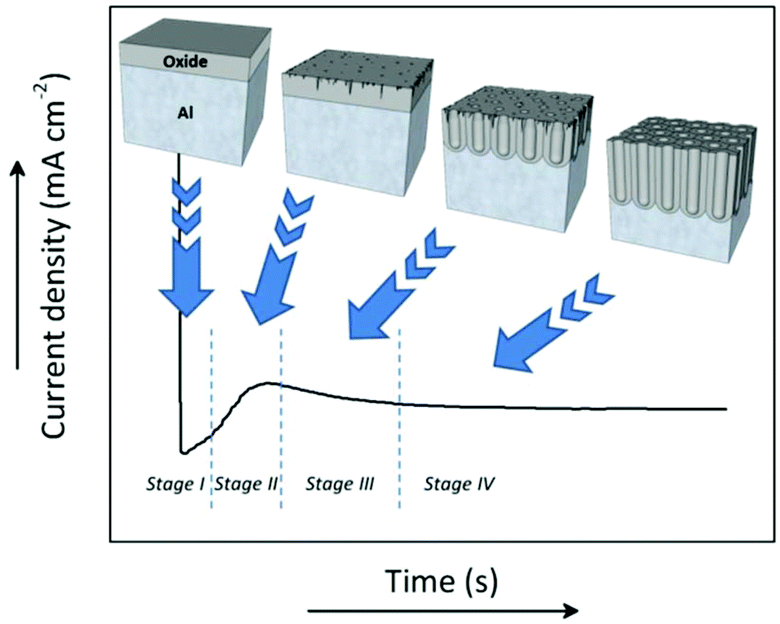 | ||
| Fig. 3 Profile of the current density-time curve recorded during potentiostatic anodization of a lab-made AAO alumina membrane prepared in 0.3 M H2SO4 at 25 V. The above-inserted illustrations show the changes occurring at the different stages, from the formation of the non-porous oxide barrier layer (stage I) to the development of pores in an ordered hexagonal arrangement (stage IV). Going through several intermediate states, the generation of defects and cracks in the surface of the oxide barrier layer (stage II) where the current will accumulate creates space for the nucleation pore sites, acting as precursors for the initiation growth of bigger pores (stage III). | ||
The chemical reactions involved in all the different stages of the anodization process in acidic media between the metal/oxide interface and oxide/electrolyte interface are as follows:
| 2Al3+(ox) + 3O2−(ox) → Al2O3 | (3) |
| Al2O3 + 6H+(aq) → 2Al3+(aq) + 3H2O(l) | (4) |
| Al3+(ox) → Al3+(aq) | (5) |
| 2O2−(ox) → O2(g) + 4e− | (6) |
| 2H2O(l) → O2−(ox) + OH−(ox) + 3H+(aq) | (7) |
The formation of anodic oxide occurs at the metal/oxide interface, as described by reaction (3), while the dissolution of anodic alumina occurs at the oxide/electrolyte interface, as shown by reaction (4). Reaction (5) corresponds to the direct ejection of Al3+ ions from the metal surface towards the electrolyte, due to an applied electrical field. Reactions (5) and (6) reduce the efficiency of the anodization process, while reaction (7) is the dissociation of water molecules occurring at the oxide/electrolyte interface. O2−/OH− ions migrate towards the metal/oxide interface under an electric field, providing new ions to form the anodic oxide.
3.1 Stage I
The exponential decay of the current density in this stage is associated with the fast formation process of the oxide barrier layer, since the electrical resistance increases due to the insulator nature of the forming compact oxide layer, which gets thicker with time. Several models describe this ionic migration through the oxide layer, describing the observed current under potentiostatic conditions, and setting different effects that determine the final rate obtained, including the classic models of Verwey, where the transport of ions within the oxide film is considered determinant,128 Cabrera and Mott, where the rate is determined by the transport across the metal-oxide interface,129 and Dewald, where the transport of ions across the oxide-electrolyte interface is also accounted for.130 In the 90s, novel approaches such as the point defect model, including the dissolution of the oxide film and the presence of point defects in it,131 and the Lohrengel model, where a hopping mechanism of the ions is considered,132 were developed. The most recent studies on the conduction through thick porous oxide films consider not only the diffusion and migration of the ions, but also stress-induced material flow and other contributions to the mass transport,133 which have shown importance in the process at this stage.3.2 Stage II and III
The increase in the current density at this stage corresponds to initial pore nucleation, which continues until a local maximum is reached. This maximum is associated with the breakdown of the oxide barrier layer and the actual development of an incipient disordered porous structure. Different theories have been proposed to shed some light on the question: what is it that sets into motion pore nucleation after the fast formation of the oxide barrier layer? Two main theories try to explain the pore nucleation mechanism occurring at this stage, namely the field-assisted model and the stress-driven mechanism. The field-assisted model, which was developed by O'Sullivan and Wood,95 suggests field-assisted pore formation. The current concentration of local imperfections on the initial barrier layer will lead to the non-homogenous growth of this layer. Pore nucleation points emerge at the thinner regions of the oxide layer. The stress-driven mechanism was developed by Shimizu and Thompson.134 They proposed a model where the stress is the key factor for the evolution of pores. Stress originates at the metal/oxide interface as a result of volume expansion at this interface as the metal substrate is being oxidized. This tensile stress contributes to local cracking of the anodic oxide film (over protuberances or ridges found in the metal surface due to imperfections or impurities). A high local current density occurs at the cracked sites and ions are consumed from the aluminium base to heal these regions, resulting in non-uniform film growth.Between these two theories, i.e., the field-assisted model and the stress-driven mechanism, the former is the most accepted and cited to explain pore initiation.
3.3 Stage III and IV
A steady state is reached as the density of pores is reduced. The disordered pores start to merge and pores parallel to each other and perpendicular to the surface start to grow. The current density decreases and when the final steady state is achieved, the current density stabilizes. A schematic representation of steady-state oxide growth and the chemical reactions involved in the process are shown in Fig. 4.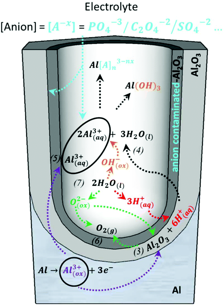 | ||
| Fig. 4 Chemical reactions of the species present in the acidic electrolyte during the anodization process: purple arrows point the route of the metallic aluminium of the substrate as it is oxidized towards the formation of Al2O3 or the direct ejection of the oxidized Al3+ ions into the electrolyte, corresponding to reactions (3) and (5), respectively. The green arrows point to the inward migration of O2− species to form new Al2O3 (reaction (3)) from the dissociation of water molecules, according to reaction (7), and indicates the generation of oxygen bubbles as O2(g) is released, as described by reaction (6). The red arrows mark the dissociation of water into H+ ions (reaction (7)) and the role played by these H+ ions in the re-dissolution of the already formed Al2O3, as shown in reaction (3). The orange arrows show the dissociation of water into OH− ions (reaction (7)), which later react with the Al3+ species present in the solution. The black arrows show the re-dissolution of Al2O3, as in reaction (4), and the formation of Al-based soluble complexes. The blue arrows mark the inward migration of the counteranions from the bulk electrolyte that binds Al3+ ions in the solution to form water-soluble complexes and their incorporation in the Al2O3 of the outer walls of the pores. | ||
During this steady stage, the thickness of the barrier layer (tb) is kept constant and the porous structure grows in thickness through the balance of two competitive mechanisms: aluminium oxide formation and dissolution of the oxide, as described by reactions (3) and (4), respectively. The formation of new anodic oxide is possible due to the diffusion of oxygen-containing ions and molecules (O2−, OH−, etc.) from the electrolyte towards the metal/oxide interface (reaction (7)). The Al3+ ions travel through the barrier layer and are ejected to the electrolyte, as shown by reaction (5). Both the dissolved Al3+ ions, according to reaction (4), and the ejected Al3+ ions, as shown in reaction (5), now present in the electrolytic solution will form water-soluble complexes with the counteranions, [A−X], of the different electrolytes. Another important event is the incorporation of the counteranions on the surface of the pore walls in close contact with the electrolyte solutions, forming an anion-contaminated outer layer of alumina along the pores. Even though it is not yet completely understood, these anionic species play a crucial role in the development and self-arrangement of the pores. All reactions are schematically represented in Fig. 4, and after a certain time, all the different reactions that are involved reach their steady-state value. This dynamic equilibrium between oxide formation and oxide removal taking place at the different interfaces has been studied under different perspectives to understand the mechanism that leads to pore formation and the steady-state growth stage, including Joule heat-induced dissolution at the pore base,98,135–137 field-assisted oxide dissolution,95,136,138 and more recently, the stress-induced plastic flow model139–142 and the effect of the bubble mold model, which has been developed to understand the evolution of different pore morphologies during their growth.143
The first approximation, that is, Joule heat-induced dissolution at the pore base, was abandoned by Nagayama and Tamura back in 1968 upon calculating that the heating at the bottom of the pore was ∼0.06 °C, and thus they considered it negligible.144 Although other authors such as Mason145 and Li and Zhang98 found that the temperature increase of the bottom of the pores was about 25 °C, that is, several orders of magnitude higher, even this temperature is not enough to explain why the growth rate at the pore base is higher. Actually, Oh,146 in 2010, based on the previous work from Hunter and Fowle,147 showed that to explain the faster growth rate at the pore base based on the Joule heat, the electrolyte should be boiling. Thus, because of all these arguments, the idea of the Joule heating was ruled out.
O'Sullivan and Wood95 developed an ‘average field model’ in which growing pores of different sizes will experience different electric fields, and thus different dissolution rates. Through merging and self-arrangement of the pores, the electrical field experienced by each pore will balance to the same average electric field. Under this average field, the equilibrium of the growth rate is achieved for all pores. Several mathematical models were developed to describe this field-assisted oxide dissolution process. Most of them used the Laplace equation,101,148,149 which assumes no space charge, to govern the potential distribution in the oxide film. At high electric fields (such as that maintained at the pore base), diffusive transport can be neglected since ionic conduction is the dominant mechanism controlling interface motion. These models were able to predict the linear dependence of the interpore distance (or cell size), Dint, with the applied potential.
This field-assisted model was modified to consider several experimental findings. For instance, in 2006, Houser et al.150 demonstrated that the Laplace approximation to describe the interface motion violates two physical conditions that were experimentally observed, namely the requirement that the interface speed must be constant, and thus the morphology of both interfaces remains time-invariant during steady-state growth. Also, the requirement of current continuity along the oxide film, which controls the actual growth, being responsible for both the recession of the barrier layer at the bottom of the pores and the accumulation of oxides on the pore walls. The authors showed that when only the Laplace equation is used, and therefore no space charge is present in the model, two effects occur, i.e., an unrealistic increase in the electrical field from the pore bottom to the ridges and a difference in current density by 7 orders of magnitude between the metal-oxide interface and oxide-solution interface (violating the current continuity observed experimentally). This implies that a certain space charge in the oxide is necessary to maintain current neutrality in non-planar oxide films. Therefore, to avoid these inconsistencies, Houser et al., also in ref. 150, proposed a current continuity equation based on the interface kinetics, accounting for Al3+ dissolution in the electrolytic bath and O−2 migration into the film. After these findings, Su et al. presented a new mathematical model supporting the equi-field strength empirical model, which was firstly described by O'Sullivan, but also including both the oxide dissolution and oxygen migration rates and in which the latter, determined by the water dissociation rate, plays a key role in the final porosity (the pore to cell size ratio).151
Subsequently, previous experimental studies employing 18O isotopes tracers were carried out first by Siejka and co-workers152 and later corroborated by Skeldon et al.,153 which showed no appreciable oxygen dissolution from the film. Then, if there is no significant oxide dissolution occurring during steady-state pore formation, the recession of the oxide-solution interface had to be attributed to other phenomena. In this line of thought, other authors supported the relevance of the direct cation ejection mechanism, where the free volume left by the ejection of Al3+ ions (according to reaction (5)) must be compensated by an inward movement of the oxide at the oxide-solution interface. This direct ejection of Al3+ ions from the substrate towards the electrolyte reduces the efficiency of the formation process of porous alumina, as was proved by Takahashi and Nagayama.154 They reported that about 40% of Al3+ ions are lost to the electrolytic solution and do not contribute to the formation of porous alumina. It is worth mentioning that several other works support the direct cation ejection mechanism.152,153,155
Then, even though the field-assisted model describes the pore-growth process and oxide formation, several experimentally observed phenomena are not compatible with it. Thus, in 2008 a new model was proposed by Skeldon et al.,139,156 who suggested a flow mechanism to explain the steady-state pore formation. In this model, the thickness of the barrier layer, tb, is kept constant by the flow of oxide materials from the base of the pore towards the cell boundaries, as was experimentally observed from the flow pattern of tungsten (W) found along the pore walls in W tracer studies. This is the opposite of the field-assisted migration of W6+ ions through the oxide towards the oxide-solution interface and their dissolution in the electrolytic bath. Moreover, this flow model is also supported by the stress-driven transport theoretical model proposed by Hebert and Houser,140,141 in which ion migration is described by combining a mechanical stress gradient and an electrical potential. The model also incorporates the viscoelastic creep of the oxide. The calculated values using this model matched the experimental results (from stress measurements to tracer studies). The authors concluded that the stress field driving the flow originates from volume expansion at the metal/oxide interface, different migration rates of O2−/OH− species and Al3+ ions, and incorporation of acidic anionic species from the electrolyte solution into the oxide.141,142 It is also consistent with Sato's breakdown model,157 in which the formation of porous alumina films was associated with continuous plastic deformation of the oxide.
Besides these theories on the pore evolution and pore growth mechanisms along the steady stage, after the nucleation initiates, there is another phenomenon that occurs in AAO nanopore membranes, which is self-ordering, that should also be understood to be able to control it. This ordering of the pores in a close-packed hexagonal arrangement also takes place at this stage. Jessensky120 and Li158 stated that stress is the driving force responsible for this alignment due to the repulsive forces between neighboring pores. Nevertheless, there is still research being done to fully understand how the different phenomena affect the actual formation mechanism and self-ordering of the pores, such as volume expansion and anion incorporation from the electrolyte solution. Both seem to linearly depend on the applied anodizing voltage,159–163 whereas the latter, at least in the particular case of sulfur incorporation, seems to increase the plasticity of the oxide since the breakdown limit of the oxide before cracking under mechanical stress is increased.163 This can open new regimens under high stress (due to higher volume expansion of the oxide) for the self-ordering formation of nanoporous alumina.
Recently, an extended version of Hebert and Houser's stress-driven plastic flow transport model was proposed,164–167 which also explains this self-ordering. In this case, the internal stresses developed in the oxide film and metal-oxide interface discussed above will also be responsible for the ordering of the pores. It accounts for volume expansion at the metal-oxide and oxide-solution interfaces due to the formation of Al2O3 and the incorporation of oxyanions, respectively, in the generation of stress driving the oxide flow. The dynamics of the interfaces is described here by dynamic boundary conditions. A non-planar topography oxide surface, inducing non-uniform current distributions at the interfaces, was also accounted for in the model. Generally, the model was able to predict the generation of tensile and compressive stress gradients from the oxide bulk towards the metal-oxide and oxide-solution interfaces, respectively, under high electrical fields, to balance the presence of O−2 or OH− ions (increasing the oxygen flux) needed at the interfaces to maintain the volume balance boundary conditions established at each of them. They observed the formation of nanometer-thick layers of interfacial stress depending on the local current density, followed by induced stress relaxation due to the oxide flow. At high electrical field conditions (under which self-ordering is achieved), the developed stress at the metal-oxide interface is tensile. Al3+ ions are consumed at a faster rate (aluminium oxidation is enhanced) than that of oxygen migration towards this interface. Tensile stress is generated at this interface to increase the volume flux of oxygen ions. However, in a later study, they suggested that the volume change at this interface is relatively small and the generated flow at the metal-oxide interface can be considered negligible. Thus, the motion of this metal-oxide interface is mainly controlled by electrical migration.167
In the same work, the motion of the oxide-solution interface is described as driven by oxide flow generated from interfacial stress. At the solution interface, strong adsorption of anionic species occurs, which coordinates with Al3+ surface ions, thus blocking oxide formation at this interface. Instead, O2− ions incorporated from the solution are forced to migrate within the oxide and interfacial compressive stress is needed to enhance the migration rate of oxygen ions. Their studies revealed that pattern formation is associated with a critical efficiency value for oxide formation, εO, just slightly higher than that of the transport number of oxygen ions, tO, by migration. Hence, compressive flow in close competition with oxide formation at the pore base is responsible for the formation of patterns of stable pores. The dimensionless parameter, ωs, which controls oxide formation is then:
| ωs=εO − tO | (8) |
In this competitive situation, a pattern emerges at the surface of the solution interface with a characteristic wavelength, λc = 2πh/kc (where h is the oxide length, and kc is a spatial dimensionless perturbation parameter), the value of which determines the interpore distance, Dint, between self-ordered pores.
The inset in Fig. 5a shows that for negative values of ωs (εO < tO), there is no perturbation peak, kc, indicating that the formation of pores is not favorable, resulting in non-porous planar films. Intermediate values of ωs ranging from 0 to 0.3 correspond to efficiencies, εO, between 0.60–0.90, which are in good agreement with the experimental efficiencies for different acids.168–170 In this range, pattern formation is promoted. The transport number of oxygen ions was set as 0.60, as reported in the literature.154 For ωs values higher than 0.3 (εO ≫ tO), the oxide is unstable (Fig. 5a), the growth rate increases at large wavenumbers, and hence no ordered pores with wide pore distributions will be formed in this regime.
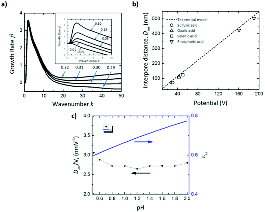 | ||
| Fig. 5 Results of linear stability analysis of the anodization model. (a) Effect on growth rate dispersion curves for Al of the parameter ωs, controlling the oxide formation rate at the oxide-solution interface near the critical value of 0.30, above which the film is unstable at all wavenumbers. Inset shows the dispersion curves below the critical value ωs < 0.30. (b) Comparison of predicted (solid line) and measured interpore distance, Dint, for anodic alumina grown in various solutions (black open symbols). (c) pH dependence of predicted Dint and anodization efficiency, εO, for Al anodization at 10 mA cm−2, for comparison to pH-independent Dint reported in the literature.102,103 Reprinted with permission from ref. 167. Copyright © 2020 Elsevier. | ||
This model also agrees well with the observed experimental dependence of the interpore distance, Dint, with the applied voltage, as can be seen in Fig. 5b. In this figure, experimental measurements of the pore spacing are plotted together with the calculated values from kc (solid line) according to the expression Dint/V = 2πhV/kc, where hV is the anodizing ratio (ratio of the barrier layer thickness to cell voltage), which has been reported to be 0.1 nm V−1, independently of the electrolyte composition. Moreover, they were able to predict using the flow model the weak dependence of the inter-pore distance on the pH of the solution, which has been also experimentally reported102,103 (Fig. 5c).
Finally, the oxygen bubble mold model accounts for the effect that the oxygen bubbles that are produced as a side reaction during anodization have on the morphology of the anodic oxide layer.143,171 As will be seen in section 5, besides pores with parallel walls, different pore-wall morphologies can be obtained, such as serrated walls172,173 and diameter modulated pores (also called bamboo-like structures),174 and these morphologies can be understood based on the oxygen bubble mold model. As hinted by its name, this model considers the oxygen generated while oxidation is occurring during anodization. Then, the generated oxygen bubbles are presented as molds for the formation of a semi-spherical barrier layer at the bottom of the pores. This model is also related to the previous one because the plastic flow of the produced oxide is enhanced by the high-pressure areas under the oxygen bubbles, where there is also a higher electric field. Then, there is a plastic flow from the bottom of the pores towards the pore walls, which is favored by the bubbles. In 2008, Zhu K et al. presented work on how the oxygen bubble mold effect can be responsible for morphologies such as serrated walls,143 where the formation of further oxygen gas bubbles at the pore wall during the pore growth results in the formation of new pores with a certain depth within the oxide layer, which gives the resulting serrated structure.
It is worth mentioning that the formation of some special morphologies that have been observed under certain anodization conditions, such as ordered nanofibers or nano-petals,175 can only be explained with both the oxygen bubble mold and plastic flow models. Nevertheless, research on the full understanding of how the hexagonal ordering of the pores is achieved is still underway. Studies such as that presented in 2020 by Heinschke et al.176 and the recent work of Pashchanka177 also presented in 2020 are examples of the current research in this direction. In the former, a mathematical model that explains how the microscopic processes involved in the formation of the pores are related to the entropy of the system that generates because of ion migration is developed. A clear relation between the entropy production and the porosity number, p, and hence the cell size, was established. Moreover, this model considers the accumulation of charge due to the incorporation of anions present in the electrolyte at the oxide/electrolyte interface and responsible for the generation of ionic flow in the interface proximity as attractive Coulomb forces compete with repulsive ones between charged ions of the same sign. This ionic flow is produced as a result of the applied anodizing potential in the electrochemical cell and is responsible for the formation of convection cells, which ensure the hexagonal arrangement of the pores. This study is based on the empirical model proposed by Pashchanka et al.,178 which predicts the optimum anodization conditions required to achieve the maximum degree of order of the porous structure and where the porosity number is the determinant factor. In the latter, Pashchanka, after studying the different theoretical models proposed in the literature for pore-formation, presented a step further in the study of the self-organization of the pores in AAOs and, modifying the conventional experimental conditions, achieved a long-range ordering in hierarchically organized cells directly on the surface of aluminium.
Thus, work still needs to be done to deeply understand the actual nature of pore formation, self-ordering, and anodization evolution. Any step in this direction, as shown in this section, opens the door to further developments and new morphologies in AAO nanoporous structures.
4 Anodization regimes
Regardless of the existing discrepancy between the different theories that have been developed to try to explain the mechanism behind the formation of the porous anodic oxide structure as opposed to barrier-type oxide growth and the phenomena that govern the self-ordering of the pores, the generated electrical field across the barrier layer (and thus applied anodizing potential) is a determining factor for oxide dissolution, Al3+ ejection and stress generation due to volume expansion at the metal/oxide interface. Therefore, an important effort has been done in this direction through the optimization of the anodizing potential. Regarding this parameter, two different regimes can be distinguished, i.e., mild anodization (MA) and hard anodization (HA), which will be described next.4.1 Mild anodization
Mild anodization conditions refer to anodization in a potential range below the breakdown potential of the forming oxide layer. Above this breakdown potential, typically the burning and cracking of the oxide or oxide formation with an increasing number of growing defects occurs.Self-ordering of the nanoporous structure of anodic alumina under this regime was first reported by Masuda et al.179 in a two-step anodization process using 0.3 M oxalic acid, as described in Fig. 6. During this process, the first anodization step was carried out at 40 V and 0 °C for 24 h. After this long anodization period, the self-arrangement of the pores at the metal/oxide interface was achieved. The end of this step is the removal of the oxide porous layer formed by chemical etching in 6 wt% H3PO4 and 1.8 wt% H2CrO4 mixed solution. Then, the surface of the remaining aluminium substrate presents a hexagonal pattern structure, which will facilitate the growth of highly ordered pores in the direction normal to the substrate. The second anodization step was performed under the same conditions as the first anodization. Later, the optimized conditions for the growth of highly self-ordered systems in 0.3 M H2SO4 and 0.3 M H3PO4 were reported to be 25 V (ref. 117) and 195 V,116 respectively, at 0 °C, and correspondingly the cell sizes of 65 nm in sulfuric acid and 500 nm in phosphoric acid (as recorded in Table 1) were achieved. More recently, other acidic systems have been studied and new conditions have been discovered, which allow self-ordering of pores with a wide range of cell sizes (see Table 1).
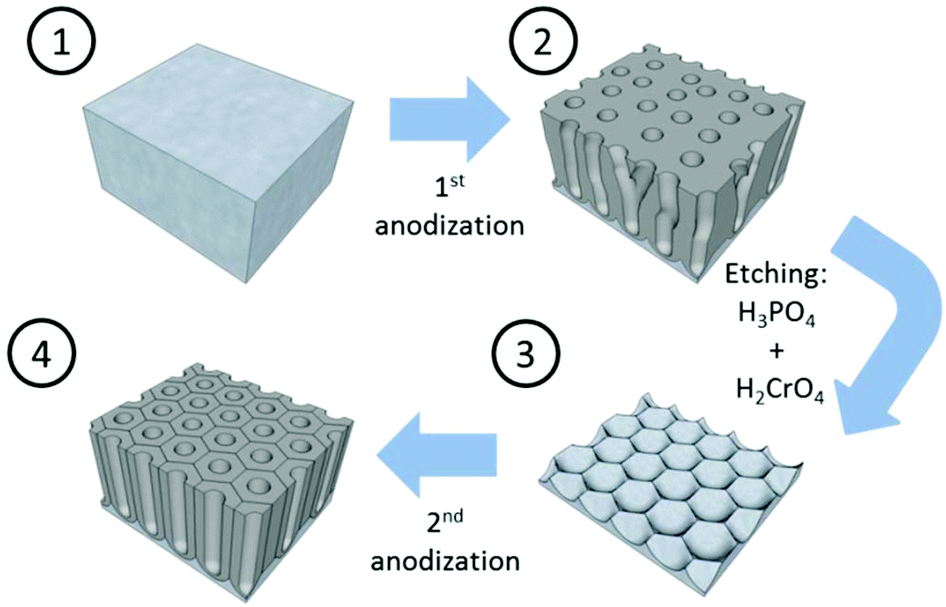 | ||
| Fig. 6 Schematic sketch of the steps involved in the two-anodization process developed by Masuda et al.179 to obtain highly ordered nanoporous alumina. | ||
4.2 Hard anodization
Hard anodization is performed under limited conditions above the breakdown potential, which is normally used to obtain thick AAO films in short anodization times. As previously mentioned, burning, cracking, or defects over the oxide appear under this regime and normally no control of the structural parameters of the pores, such as pore diameter and interpore distance, was possible to be achieved until quite recently. To improve the control and avoid the breakdown of the oxide under a high anodizing potential, one approach is to use additives, which will improve heat dissipation (e.g. by adding ethanol)5,6 or increase the electrical resistivity of the electrolyte solution, thus increasing the limiting breakdown potential (e.g. by the addition of ethylene glycol).118 Also, mixed solutions of acids have been successfully used in HA anodization conditions.113,123,125,126 However, the most popular procedure involves a first anodization step under MA conditions followed by a gradual increase in the anodizing potential until reaching the HA regime.2,4,113,121,123,125,126 Details of the structural parameters of the AAOs fabricated under HA conditions are recorded in Table 1.When very high voltages are applied, besides porous growth, the different cells can be cleaved due to the high rate of O2− and OH− ions travelling through the barrier layers, creating tensile stress near the cell ridges, which has been observed experimentally by the formation of nanotubes, for instance in ref. 140. Also, a variation in the cell wall thickness when HA in oxalic acid is performed at ultra-high voltages has been reported, which is related to the oxygen gas bubbles created at the metal-oxide interface.171 Also, in this regime, the formation of a certain amount of Al(OH)3 has been observed, which is another important difference with MA, and thus, the mechanisms governing this regime are different.
In 2015 Vega et al.5 proposed a specific mechanism for the formation of pores under HA conditions, which supposes a breakthrough in this particular regime, where the starting point for research was oxide burning and cracking. This mechanism was based on diffusion-limited oxide growth due to fast oxide formation under HA conditions, which hinder the diffusion of ions from the bulk electrolyte solution, oxalates species in their experiments, along the length of the pores and towards their base. They suggested that under this regime, oxide growth at the oxide/electrolyte interface becomes relevant (as in the case of non-porous-type anodic oxide) due to the limited diffusion of oxalate species (phosphate or sulfate ions, depending on the electrolyte), thus resulting in a lower concentration of these species available at the pore bottom to react with the Al3+ ejected ions and form water-soluble molecules. Instead, the ejected Al3+ ions will react in a higher proportion with water molecules, forming non-soluble complexes that finally contribute to the formation of new Al2O3 at the oxide/electrolyte interface. This phenomenon is not considered during the formation process of porous alumina films under MA conditions. An increase in the thickness of the barrier layer, tb, because of the re-deposition of Al2O3 at the pore base was expected.
By neglecting the terms associated with migration and convention contributions to the ionic transport of the Nernst–Planck equation, and assuming a linear concentration gradient along the pores, as shown in Fig. 7a, (with the form C(x) = C(0) + [C(L) − C(0)]x/L, where C(0) is the concentration of ions from the bulk electrolyte present at the pore base, which is approximated to 0 and C(L) = C0 takes the value of the initial concentration of the bulk electrolyte), they obtained an inverse relationship between the current density and the thickness of the oxide membrane according to the following equation:
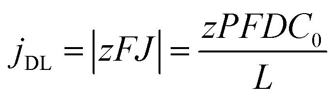 | (9) |
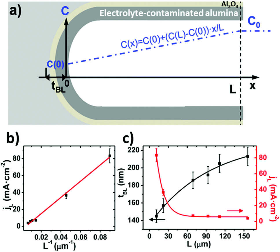 | ||
| Fig. 7 (a) Linear profile of the concentration gradient along the pore length. (b) Fitting of the final anodization current density, jL, as a function of the inverse of the total membrane thickness, L−1, obtained for H-AAO samples anodized at 120 V in 0.3 M oxalic acid electrolyte. (c) Dependence of the barrier layer thickness, tb, and limit current density, jL, on the total thickness of the alumina membrane. Reprinted with permission from V. Vega, J. García, J. M. Montero-Moreno, B. Hernando, J. Bachmann, V. M. Prida and K. Nielsch, Unveiling the Hard Anodization Regime of Aluminum: Insight into Nanopores Self-Organization and Growth Mechanism, ACS Appl. Mater. Interfaces, 2015, 7(51), 28682–28692. Copyright © 2015 the American Chemical Society. | ||
Experiments confirmed the behavior of the current density described by eqn (9), as well as the predicted thickening of the barrier layer with the total thickness of the oxide membrane. As the thickness of the barrier layer increases, the generated electric field across the layer decreases (Fig. 7c). The migration of O2− and OH− species across this oxide barrier is reduced, and thus it is the current density. They observed experimentally the linear dependence of the last current density recorded value, jL, and the inverse of the final thickness of the AAO film, L−1 (Fig. 7b), in agreement with eqn (9).
5 Different morphologies of the porous structure. Influence of the anodization conditions
The understanding and control of the anodizing conditions make it possible to obtain nanoporous alumina membranes with certain pore diameters (with low dispersion in size), ordering, and pore-lengths. The next natural step in the anodization of aluminium is the development of new fabrication techniques, modifying the fabrication conditions, which provide novel pore architectures. Among them, we will briefly describe the most relevant ones, including branched pores, where one pore is divided into others or the other way round, modulated diameter nanopores, where anodizing pulses are applied alternating between the MA and HA anodization regimens while forming a porous structure, and finally, 3D porous structures, where the conditions are highly controlled over time and can give rise to nanopore structures with interconnected pores.Furthermore, pre-patterning treatments of the aluminium surface by direct indentation methods such as focus ion beam (FIB) lithography,180–184 using the scanning probe of an Atomic Force Microscope (AFM)185,186 to generate an indention on the Al surface, interference lithography,187 reactive ion etching (RIE),188,189 and through the combination of lithographic processes and the use of resins190,191 or employing AAO and PMMA as masks192,193 followed by wet chemical etching; or by indirect impression techniques based on imprinting molds194–198 employing, for example, nanoimprint lithography technology; are used to produce long-range highly ordered nanopores with a fixed unit cell size, reducing the number of anodizing steps to achieve perfect order. However, for this goal, the first approach is time-consuming and expensive, while the second route has a limitation of the area of the fabricated mold of 1 mm2 for imprinting. Besides the high order of the pores obtained by these means, the typically hexagonal geometry of the unit cell can be altered, producing new morphologies with pores in a square and triangular arrangement.
5.1 Branched nanoporous structures
Mainly, two different approaches have been developed to achieve branching of stem pores, namely through non-steady-state and steady-state anodization. During steady-state anodization, the anodizing voltage decreases accordingly to the equal-area model, which states that the total pore area of the template is invariant, hence branching of the stem pore into n smaller in diameter pores that will follow the relation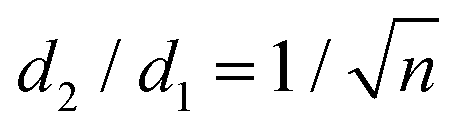 , which considers the conservation of the pore area. d1 and d2 are the diameter of the stem pore and the diameter of the n smaller branched pores, respectively. According to the previously established linear relationship between pore diameter with the anodizing potential (see section 2, eqn (1)), the equal-area model can be extrapolated to the anodizing voltage giving a reduction of the original voltage, V1, by a factor of
  . In this regimen, to obtain n Y-junctions, the voltage is systematically reduced in
  steps. Each step will be extended over time until a steady state of the current density is reached under the new anodizing conditions. To reduce the duration of these steps, researchers followed different anodization routes, including chemical etching of the barrier layer down to the correspondingly new thickness of this layer under the decrease of the anodizing voltage between each branching step199–202 and a change in the electrolyte solution to better suit the new anodizing conditions to be applied.200,203 Sousa et al.200,204 studied three cases as follows: (1) successive branching without intermediate steps (which requires long stabilization periods); (2) incorporation of an intermediate etching step between each branching process; and (3) switching of the electrolyte solution depending on the anodizing voltage to be applied. Accordingly, anodization was initially carried out in 0.3 M oxalic acid solution, and then the applied potential was sequentially reduced by a factor of
  , as shown in Fig. 8a and b. In another set of experiments, the same anodization process was reproduced; however, a chemical etching step in 0.1 M phosphoric acid was implemented between successive branching to shorten the time consumed in each anodizing step. After thinning of the barrier layer to a value corresponding to that of the applied potential (according to the expression tb = γV), the generation of branched pores occurred immediately and the duration time of the anodizing steps was reduced. However, the resulting branched structure was over etched, since chemical etching collaterally causes the widening of the pores, and extreme enlargement of the pore results in the collapse of the porous AAO films. To overcome both issues, namely over-etching and long duration times of the anodization steps, in a third experiment, the electrolyte solution was changed to 0.3 M sulfuric acid.
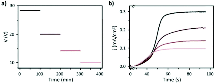 | ||
Fig. 8 Steady-state anodization: (a) recorded V(t) reduction from 28.4 V to 10 V by a factor of  to obtain two-, three- and four-generations of Y-branched pores. (b) Density current, j(t), transients with a decrease in the j(t) values due to the reduction of the applied potential, and the anodization time is extended during each voltage reduction stage until the anodization density current reaches a new stable value. Reprinted with permission from ref. 204. Copyright © The Royal Society of Chemistry 2012. to obtain two-, three- and four-generations of Y-branched pores. (b) Density current, j(t), transients with a decrease in the j(t) values due to the reduction of the applied potential, and the anodization time is extended during each voltage reduction stage until the anodization density current reaches a new stable value. Reprinted with permission from ref. 204. Copyright © The Royal Society of Chemistry 2012. | ||
Nevertheless, regardless of the shortcomings encountered, hierarchical multi-branched pores in succeeding tiers have been successfully fabricated if etching of the barrier layer is performed between each branching step.201Fig. 9b shows the top and cross-sectional views of a three-tiered branched pore structure. The fabrication process is as follows: the 1st anodization in 0.3 M phosphoric acid at 130 V for 30 min and a subsequent 50 min chemical etching step, followed by a 2nd anodization in 0.15 M oxalic acid at 80 V for 3.5 min and a 90 min chemical etching step, and a subsequent 3rd anodization in 0.3 M oxalic acid at 50 V for 15 min and a 40 min chemical etching step. Other authors also defend the need to add a chemical etching step of the barrier layer before variation of the anodizing voltage to eliminate the competitive growth of branched pores. Competition between stem pores or branched pores occurs due to the non-uniform dissolution of the barrier layer during the different anodizing steps and non-uniform field strength distribution at the pore base. Then, the pore growth rate of certain pores (or branched pores) occurs over the others. The etching of the barrier layer enables steady-state growth to be reached more rapidly under the new anodizing conditions, thus avoiding the non-uniform dissolution of this barrier layer occurring during the long periods taken to reach the new steady-state when no previous etching is performed.202
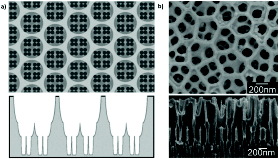 | ||
| Fig. 9 (a) Schematic illustration and (b) actual SEM images of multi-branched pores fabricated in succeeding tiers. Top view (top image) and cross-view (bottom image). Reprinted with permission from ref. 201. Copyright © 2008 WILEY-VCH Verlag GmbH & Co. KGaA, Weinheim. | ||
In contrast to the voltage-control method described above, Guo et al.205 reported a current-control method for the fabrication of highly homogeneous triple-branching pores, where the homogeneity of the branching pores is improved by controlling the applied current against the reduction of the applied potential. More complex branched structures have been grown by alternating between the voltage and current control anodizing steps.206
Similarly, Zakeri and co-workers207 proposed a model where branching of pores occurs over non-flat aluminium surfaces and without the need to reduce the anodizing voltage through the curving and subsequent merging of the growing pores over edges, notches, and curved sites.
Recently, in 2016 Jin et al.208 developed three different types of complex branched structures by combining the steady-state growth of branched pores on pre-patterned curved aluminium substrates, where tree-like porous structures are formed, as previously described by Zakeri et al.,207 at the boundaries of the pattern cells. Specifically, type 1, 3D interconnected branched structure; type 2, self-supported AAO nanowires structure, and type 3, which is what the authors called a supporting AAO skeleton structure. To obtain 3D interconnected branched pores (type 1 structure), a periodic anodizing potential was applied alternating between 50–30 V in 0.3 M oxalic acid, followed by a 35 min etching treatment. Types 2 and 3 were grown under a constant voltage (30 and 40 V) and different etching times 31–33 min (AAO nanowires were formed) and 43 min for the complete dissolution of these nanowires, respectively.
Serrated branched porous structures associated with oxygen evolution when applying different voltage steps have also been reported by several authors.143,172,173 The growth of serrated pores in the oblique direction along the vertical walls of the pore channels cannot be assessed by the field-assisted dissolution theory at the pore bottom of perpendicular pores (concerning the aluminium substrate) due to geometric considerations. Therefore, the formation mechanism of serrated pores combines the previously proposed field-assisted flow model by Skeldon et al.139,156 with the oxygen bubble mold effect. During anodization, oxygen bubbles trapped within the oxide barrier layer are generated, and current density accumulates around them. Consequently, Al2O3 formation is promoted at these local points, where the field strength is increased, a protuberance is formed and the oxygen is released from the oxide. Then, at the steady-state growth stage, protuberances are pushed towards the vertical walls by oxide flow deformation. However, this mechanism is only enhanced under certain conditions, such as at elevated anodizing temperatures at which the increase of the current density induces higher oxygen evolution and when the Al substrate is placed vertically inside the electrochemical cell, which seems to promote the formation of serrated branched pores aligned on one side of the walls of the vertical channels.
In the case of non-steady state, the anodizing potential exponentially decreases (Fig. 10a), and potential reduction steps are applied before the steady stage can be reached at each anodizing step. The transient current versus time curves show a tooth-like profile, as can be seen in the inset of Fig. 10b. The current drops as the applied potential is reduced and then starts to increase with time. However, the next potential reduction step will be applied before current stabilization is achieved (Fig. 10b).
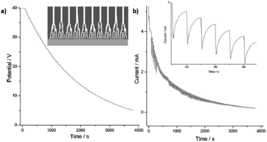 | ||
| Fig. 10 (a) Potential-time and (b) current-time transients profiles recorded in non-steady-state anodization. Inset in (a) is a schematic illustration of the tree-like branched pores. Inset in b is the magnification of the current curve for a clear view of its tooth-like profile. Reprinted with permission from ref. 209. Copyright © 2007, The Royal Society of Chemistry. | ||
Cheng et al.209 proposed a specific mechanism for the formation of branched pores under the conditions described above. They stated that when the anodization process is kept in a non-steady state, the oxide formation and dissolution rates never reach an equilibrium balance and negative charges (coming from oxygen-containing species) will tend to accumulate in the oxide layer up to a threshold accumulative charge. Then, discharging of the negatively charged oxide layer will occur, leading to the generation of non-uniform current pathways running through the oxide. Field-assisted dissolution is induced this way, resulting in the formation of branched pores. Consequently, the pore diameter of the branched pores is not proportional to the anodizing potential with a root or tree-like form (inset Fig. 10a).
In addition to the electrical field effect, the authors also paid attention to the role played by mechanical stress. One specific morphological characteristic of this type of branched pores is their uneven morphology, where some nodes can be found along with individual pores. Furthermore, when branching of a pore takes place, the stem pore will always grow into two pores smaller in diameter. This was explained as a consequence of the strong repulsive forces between neighboring pores. Repulsive forces due to space limitation reduce the ramification of a pore into only two branches if they manage to overcome these forces. If not, a node appears. In this competitive branching pore formation mechanism, pores suddenly change direction, looking for space to grow and deviate from the perpendicular direction concerning the substrate.
A slightly different concept of the branched structure was that presented in 2018 by Hashimoto et al., where the authors fabricated a membrane they described as a hierarchical structure of macropores with a pore wall full of mesopores210 by anodization of aluminium in phosphoric acid, and then, a heating process at 1400 °C produced aluminium phosphate nanoparticles, which were segregated from the alpha-alumina matrix formed after the annealing. Then, these nanoparticles were dissolved in concentrated hydrochloric acid, giving rise to the combination of straight macropores (with diameters of around 220 nm) with mesopores with a diameter in the range of 20–80 nm present inside the macropore walls.
All the branched structures described in this section can be later used for the fabrication of branched nanowires (NWs) and nanotubes (NTs) for several practical applications in different fields, namely electronics, optics, energy harvesting, and biotechnology. More details of the actual applications of Y-branched NWs and NTs will be described in section 6.
5.2 Nanopores with modulated diameters
To produce changes in the diameter while the nanopores are being formed, there are many different possibilities, such as using a modified electrolyte with additives such as ethylene glycol to modify its viscosity,212 combining constant voltage anodization and chemical etching,213 and using the HA method with very high applied voltages,214,215 where fluctuating diameters along the pore length are obtained. In the last few years, the two most commonly used methods are the change in electrolyte while performing the anodization203 (Fig. 11a and b) and maintaining the same electrolyte, while varying the applied voltage. This change in voltage can be done in such a way that periods of mild anodization and hard anodization are applied during the anodization (this technique is known as pulsed anodization).211 The latter permits the fabrication of subsequent HA and MA layers of alumina (Fig. 11c and d), and thus, the combination of their properties, including alternating layers of different porosity and refractive index.211,216 With this method, high control over the shape of the modulations and their position can be achieved. Currently, these structures are being widely used as photonic structures, as will be further discussed in section 7.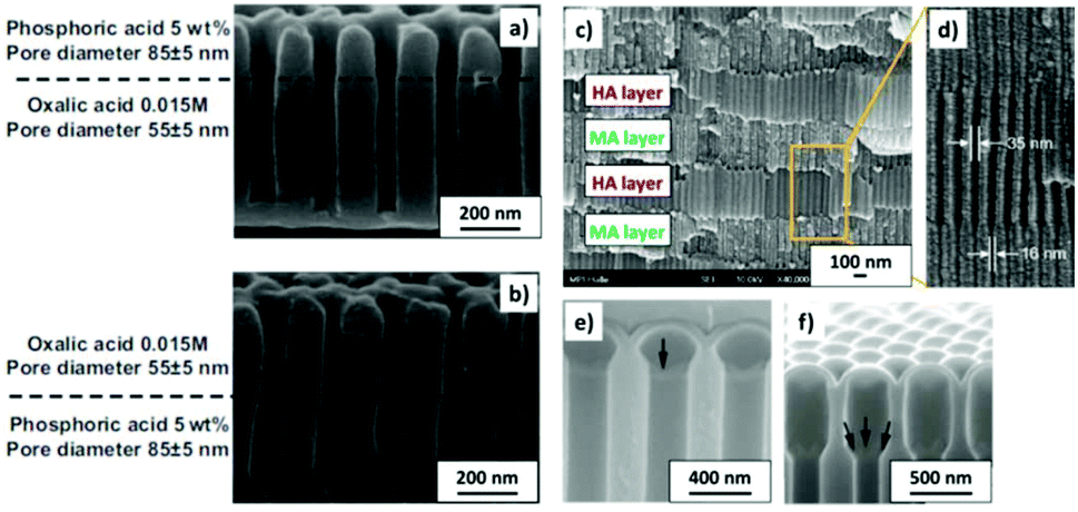 | ||
| Fig. 11 (a) and (b) Nano-funnels and inverted nano-funnels (as named by the authors). They are formed by anodizing firstly in 5 wt% phosphoric acid followed by anodization in 0.015 M oxalic acid and vice versa. The pore spacing is 200 nm and the dotted line shows the change in pore diameter. Reprinted with permission from ref. 203. Copyright © 2007 WILEY-VCH Verlag GmbH & Co. KGaA, Weinheim. (c) and (d) SEM cross-sectional view of AAO with modulated pore diameters by pulsed anodization in 0.3 M sulfuric acid at 1 °C. Each cycle consisted of an MA pulse (25 V for 180 s) and an HA pulse (35 V and 0.5 s). Reprinted with permission from ref. 211. Copyright © 2011 Elsevier Ltd. All rights reserved. (e) and (f) Cross-sectional SEM micrographs of bottle-shaped pore channels with two sections of significantly differential pore diameters after an annealing treatment at 500 °C, followed by re-anodization in phosphoric acid up to a specific current density (of 0.5 mA cm−2 and 6 mA cm−2, respectively) and then etching for 32 min. | ||
Furthermore, controlling the profile of the periodic pulsed signals, meaning the amplitude and period of the applied pulse, the shape of the pores can also be modulated, and pores with a desired geometry can be fabricated. Hence, voltages or current pulses with tooth, sinusoidal, triangle, or square profiles result in different pore geometries. This process is known as cyclic anodization and differs from the pulsed anodization technique in a slower transition from MA anodization conditions to HA anodization, which allows better control over the shape of the modulated pores.216,217 It has also been reported that cyclic anodization technique, during which the anodizing voltage (or current) is gradually increased up to HA conditions, is better suited to produce modulations along the pores when using oxalic and phosphoric electrolytes due to the longer recovery times required for both electrolytic solutions until the current density stabilizes across the barrier layer as the applied potential is increased.199,218 The forming oxide barrier layer is thicker in phosphoric acid and oxalic acid solutions than sulfuric electrolytes, and hence if pulsed anodization is used, where the transition between MA and HA regimens happens at a faster rate, a current steady state is not reached during the applied HA pulses and the changes of the anodizing voltage (or current) do not result in the actual modulation of the pore structure for the former cases. The barrier oxide layer of sulfuric AAO membranes is thin enough, and thus control over the pore geometry can be attained through pulse anodization.
Fig. 12 shows the modulated pores with different shapes fabricated by cyclic anodization processes. When asymmetric current pulses with an exponential tooth-like profile are applied, asymmetric pores are also obtained with an asymmetrical bottle-neck type geometry, as can be seen in Fig. 12a. As expected, with symmetrical sinusoidal pulses, the resulting pores present an asymmetric spherical shape (Fig. 12b). Finally, a more complex multilayer pore structure with different geometries can be obtained by combining tooth-like and triangular pulses, as shown in Fig. 12c. Insets 1, 2, and 3 show in more detail the different features of the modulated pores obtained by the different profile periodic pulses that appear underneath each of them.
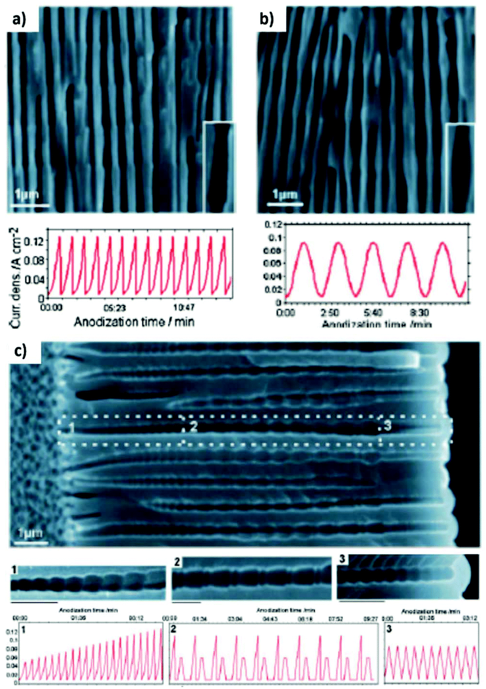 | ||
| Fig. 12 Controlling the shape of the AAO-modulated pore by cyclic anodization. Current–time curves and corresponding SEM images of AAO pore structures fabricated by galvanostatic anodization in 0.1 M phosphoric acid at −1 °C using different current signals. (a) Asymmetrical current signal with an exponential saw-tooth-like profile with asymmetrical bottle-neck shaped pores. (b) Symmetric sinusoidal current signals showing pore segments with spherical shapes. (c) Combination of (1) asymmetrical current signal with an exponential saw-tooth-like the profile of increasing amplitude, (2) alternating asymmetrical (saw-tooth-like profile) and symmetric (triangular) current signals, and (3) final series of symmetrical triangle pulses for the fabrication of AAO with more complex pore architectures. Reprinted with permission from ref. 217. Copyright © 2009 Wiley-VCH Verlag GmbH & Co. KGaA, Weinheim. | ||
In both cases, pulsed anodization and cyclic anodization, the thickness of each segment can be controlled by the duration of each pulse. However, the mechanism behind the change in the geometry of the modulated pores is not yet well understood. It seems that the key factor is the difference between oxide formation and oxide dissolution rates as the anodizing conditions are varied (HA/MA anodization regimens) and that the electric field continuously changes throughout the process. Comparing the curvature of the barrier layer formed during the different stages of the cyclic anodization process (HA, MA and the transient time in between) from the SEM images taken at each of them, it was observed that during the HA condition, the barrier layer possesses a more ellipsoidal shape, while in the other two stages, the barrier layer has a more circular geometry. These experimental findings indicate that the different formation and dissolution rates at each of the different stages of the periodical pulses indeed affect the shape and morphology of the resulting pores.217
Other combinations of anodization conditions, etching, annealing, etc. have also been explored to give rise to pore morphologies such as bottle-shaped pores in the base of the pores, like in ref. 219, (see Fig. 11e and f). During this process, the prior annealing treatment reduces the etching rate of the pore walls, while that of the barrier layer is enhanced by the subsequent re-anodization processes, and the preferred chemical etching around this oxide layer (probably due to structural changes induced by the annealing treatment) results in the generation of scalloped pored tips at the bottom of narrower channels (bottle-shaped).
Another approach involves temperature-modulated hard anodization, which was developed by Bayat and co-workers.220 In this process, the current density, and hence pore diameters, were varied by temperature modulation under hard anodization conditions. Anodization was carried out in 0.075 M oxalic acid solution containing 10 v/v% ethanol at −4 °C, and 130 V starting potential. After 10 min the anodizing voltage was gradually increased to 230 V, and at this potential, the anodization was extended for 1 h. During this time, the temperature was periodically increased, which in turn caused an increment in the current density, and then decreased again back to the steady state. Using this method, cylindrical pores with modulated diameters were successfully fabricated, with narrow segmented pores of 47 nm in diameter and the widest segments of 130 nm.
A recent development, which is linked with this pulsed anodization technique, is the fabrication of ultra-short anodic alumina nanotubes (AANTs), where galvanostatic pulsed anodization is performed using ultrashort pulses of HA (of one second) in an electrolyte with a certain amount of ethanol. Control over this process is achieved by the optimization of three factors, which are deeply intertwined, i.e., current density, HA duration, and heat generation. Short HA pulses of 1 s are required to produce ultra-short AANTs; however, when these HA pulses are shortened incompletely, voltage recovery occurs (in other words, the maximum HA voltage is not reached) and modulation of the pores is not observed. HA anodization is associated with the large evolution of heat compared to MA and accelerating oxide dissolution rates. To favor the generation of modulation due to the thinning of the pore wall structure under fast applied HA pulses, heat generation must be enhanced under a certain fixed current density. Accordingly, the authors found that the addition of ethanol, while the electrolyte was kept above 0 °C, did not contribute to heat dissipation, but on the contrary, contributed to increasing it. Besides, heat generation produces weakened conjunctions along cell boundaries as well as weak MA/HA interfaces, which can be then cleaved and individually separated after acid etching and subsequent sonication of the structure. Consequently, well-defined AAO nanotubes were produced.221
5.3 3D porous structures
These structures provide a further step to the modulated nanoporous structures considering that the fabrication principle is similar, that is, a periodic change in the anodization conditions switching between MA to HA by either pulsed or cyclic anodization. Nevertheless, in this case, precise control over the anodization parameters is required to obtain a 3D interconnected porous structure, in which the longitudinal pores are connected to other 6-neighboring pores through transversal nanochannels. In particular, the etching times must be precisely adjusted so that selective chemical dissolution at certain positions along the pore channels, corresponding to the HA pulses, is achieved. Simultaneously, excessive etching must be avoided, which will revert to the collapse of the whole porous structure. The higher content of impurities and less density of the HA layers make them less chemically stable against chemical etching compared to MA layers, and hence selective etching of HA layers is accomplished.In 2009, 3D nanoporous structures (grown in 0.1 M phosphoric acid using cyclic anodization under galvanostatic mode) were fabricated by Losic and co-workers,223 as shown in Fig. 13a, combining longitudinal nanopores of around 250 nm in diameter and transversal nanochannels with dimensions of 60–100 nm in diameter, located periodically along the length of the former. Accordingly, the porosity of the alumina membranes was significantly increased. Later in 2014, Martín et al.222 developed a pulsed anodization controlling-voltage procedure, in which 3D nanoporous networks with longitudinal pore diameters of 45–50 nm and transversal pores of 25–30 nm in diameter were synthesized in 0.3 M sulfuric acid electrolyte (Fig. 13b and c). Following this approach, these structures have been even fabricated in cylindrical aluminium wires,224 which demonstrates the good reproducibility and consistency of the method.
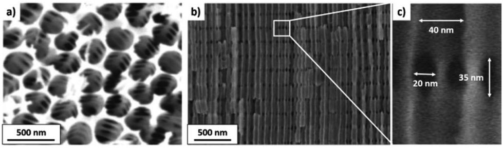 | ||
| Fig. 13 3D network porous structures consisting of a hexagonal array of vertical pores, which are periodically interconnected through transversal nanochannels to adjacent longitudinal pores at certain points. (a) Fabricated by current-controlled cyclic anodization in 0.1 M phosphoric acid. Reprinted with permission from D. Losic and D. Losic Jr, Preparation of porous anodic alumina with periodically perforated pores, Langmuir, 2009, 25(10), 5426–5431. Copyright © 2009, the American Chemical Society. (b) and (c) Fabricated by voltage-controlled pulsed anodization. (c) Enlarged view of the area marked in b with a square in which longitudinal pores (diameter = 40 nm) and the transversal pores (diameter = 20–35 nm) can be distinguished. Reprinted with permission from ref. 222. Copyright © 2014, Springer Nature. | ||
These 3D porous alumina membranes by themselves have been proven to be useful in many different applications, as will be thoroughly shown in section 7. Also, they have been used as templates for the fabrication of interconnected arrays of nanowires of a wide variety of materials, as will be discussed in detail in the next section.
5.4 Pre-patterned structures on the alumina surface
As previously mentioned, pre-patterning of the aluminium surface before the anodization process of the substrate can be carried out by two different methods through a direct approach or an indirect one, resulting in the perfect arrangement of pores. A monodomain porous structure can be relevant for certain applications in photonics225–229 and magnetic recording media.230 Moreover, different structures can be produced this way over the surface of alumina, resulting in different and new morphologies in which the geometry of the pore cell is changed, as shown in Fig. 14. The key factor to generate new pore arrangements in a square, triangular, hexagonal or even diamond shape is the initial arrangement of the pre-patterned concave pits over the Al substrate guiding the initiation of pores, but not the shape of the indented pits. In particular, when an FIB pattern with a graphite lattice and a 300 nm interpore distance was used, the oxide walls developed in a triangular shape (see Fig. 14a and b), and if the pattern used had a hexagonal arrangement with some missing sites but the same interpore distance (Fig. 14c) then the shape of the visible oxide walls was diamond (Fig. 14d). A final example of a rectangular arranged pattern of holes with 300 nm for the long and nm for the short interpore distance is shown in Fig. 14e, which also produces a rectangular arrangement of pores after anodization (Fig. 14f). The SEM images corroborate that the final arrangement of the pores is only dependant on the arrangement of the pattern. It is also worth mentioning that more complex arrays based on Moiré patterns, which consist of the superposition of hexagonal patterns with a rotation angle, with several different interpore distances have been reproduced in the surface of alumina via nanoimprinting lithographic techniques,182 as shown in Fig. 14g and h.
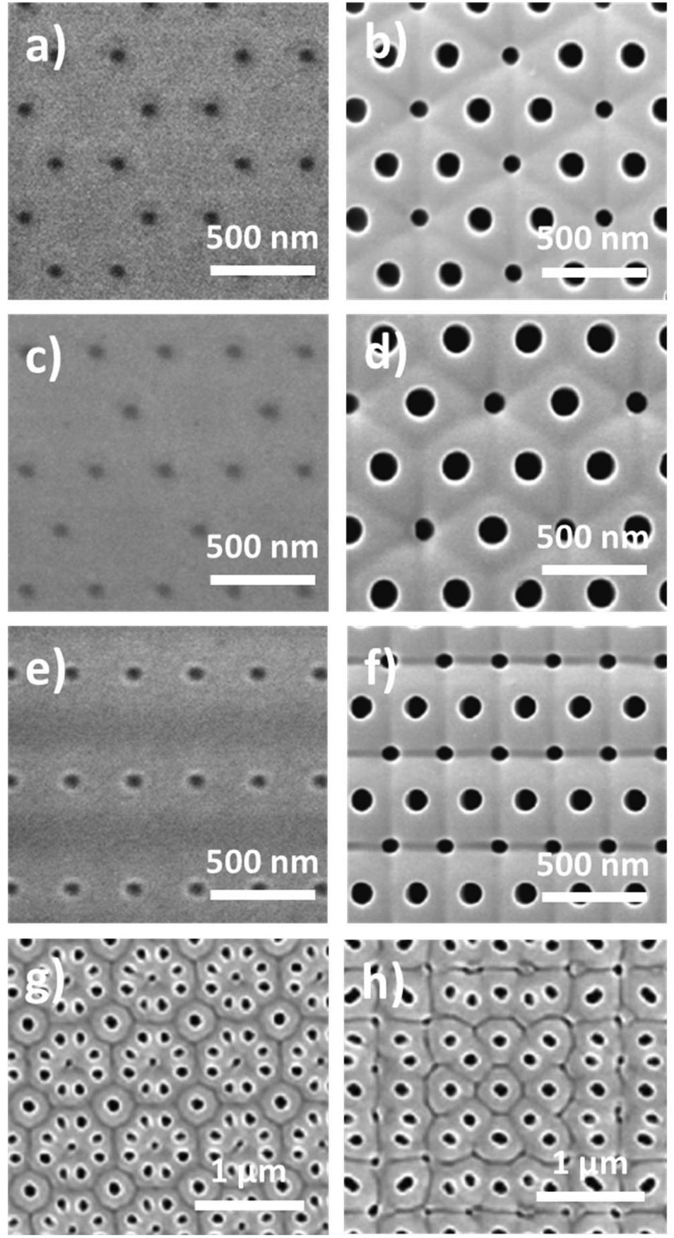 | ||
| Fig. 14 FIB patterned concaves with (a) graphite, (c) hexagonal and (e) rectangular lattice structure, where the interpore distance between concaves is 300 nm in all cases. (b) and (d) and (f) corresponding SEM images to the FIB patterns in (a), (c) and (e) after anodization in 0.3 M phosphoric acid at 20 mA with a steady-state potential of 140 V, respectively. Reprinted with permission from ref. 180. Copyright © 2011, the American Chemical Society. (g) and (h) SEM images of the porous surface of alumina with a Morié pattern created from two overlapping square patterns with the same interpore distance (350 nm) and two square patterns with different interpore distances (400 nm and 500 nm), respectively. Nanoindentations were performed with a rotational angle of (g) 36.9° and (h) 0°, and the subsequent anodization was carried out under a constant current of 20 mA at 0° for 2 min, in 0.3 M phosphoric acid. Reprinted with permission from ref. 182. Copyright © 2011, the American Chemical Society. | ||
The non-hexagonal arrangement can only be maintained for a certain anodization duration before rearrangement of the pores occurs in a hexagonal pattern. The optimization of the anodizing potential accordingly to the self-ordering regimen conditions is also important in the case of a hexagonal unit cell, where the linear relation between the cell size and the optimal value of the anodizing voltage is 2.5 nm V−1, in agreement with eqn (2). However, a reduction in the interpore distance in a squared cell has been reported to result in a less densely packed arrangement compared to a hexagonally packed distribution, according to the following equation:231
| Dint = 1.04 × U + 33, | (10) |
In general, the introduction of indentations on the surface of aluminium, which act as nucleation sites, guides the growth and development of the pores, as well as the geometry of the unit cell. However, the nucleation of pores at the edges of the cell boundaries can be propitiated under certain conditions, and thus if the interpore distance between neighboring pores is sufficiently large, the cell boundaries become visible and new pores can be formed at the cell junctions of the imprinted pattern. This phenomenon occurred in the three different examples presented in Fig. 14, where the smaller pores in the SEM images corresponding to Fig. 14b and d, and f do not appear in the FIB pattern that was used in each case, as shown in Fig. 14a, c, and d, respectively. The common factor in these three cases is the interpore distance between the indented pits of 300 nm (long interpore distance in the rectangular pattern, along which the smaller pores arise), which seems to be sufficient distance for the development of these new pores. In this case, the electric field at the bottom of the imprinted concaves defines the size of the pore cell, while the mechanical stress guides the growth direction of the new pores forming at the cell junctions. Accordingly, not only non-hexagonal cells can be generated, but also non-spherical pore shapes are produced depending on the stress field experienced at the cell boundaries. Hence, elongated, elliptical, and triangular smaller pores are generated depending on their surroundings, where the bigger pores grow faster and will confine and restrict the growth of the former pores. More complex patterns can be created with both triangle and diamond shape pores, as shown in Fig. 15c, when an array of non-regular hexagonal polygons (inset in Fig. 15c) is employed. In these nonequilibrium arrangements, the hexagonal cell is partially compressed, leading to the formation of diamond, circular, and triangular pores. This also applies to the smaller pores in alternating size patterns, as shown in Fig. 15a, where two different sized pits of 65 and 45 nm were imprinted at a 200 nm interpore distance over an Al substrate by FIB. After the anodization, the larger pores presented a spherical shape with a diameter of 105 nm, while smaller pores grew with an elongated shape along the direction that was not restricted by the presence of the bigger pores (Fig. 15b). The long axis of the pores was 95 nm and the short axis was 50 nm, where the later the growth in the direction between two bigger pores was cut short due to the much faster growth of the oxide layer of the larger pores, thus resulting in the elongated pore shape. On the other hand, circular pores are favored when the neighboring concave patterns surrounding a particular pit have a symmetrical distribution (distance and size). Also, if the interpore distance of the patterned concave reaches the optimal value to allow the complete development of the pore, the generated pores develop a round shape.232 Moreover, as the interpore distance is further increased, the area between the cell boundaries of neighboring pores becomes too broad and new non-pre-patterned pores can form,232,233 as mentioned before. The self-formation mechanism of these pores was first studied by Masuda195 using a hexagonal pattern with a missing hole; however, after the anodization process, complete repair of the hexagonal arrangement with no missing pores was accomplished, which was described as a self-compensating healing process. The growth and complete development of these pores was also explained according to the equi-field strength model151 by several authors.180,232 A direct consequence of this self-compensating mechanism and development of new pores between far apart pores is the reduction of the interpore distance, and thus the size of the unit cell in the hexagonal arrangement, which can be used to overcome the resolution limit of technology commonly employing lithographic techniques and etching treatments to produce stamps and molds in the case of using indirect indentation methods, as proposed in ref. 232, 234 and 235. Another advantage is the possibility to reduce the optimum interpore distance value associated with the self-ordering conditions defined by eqn (2) for each of the different electrolytes, as reported by Choi et al. in 2003. In a 0.3 M phosphoric electrolytic solution at an applied potential of 195 V, the ordering of the pores occurred at an interpore distance of 500 nm; however, the authors were able to reduce this distance to 0.6Dint = 300 nm, while the ordering of the pores was not affected. Recently, nanosphere lithography has emerged as a promising technique to solve the resolution problem of conventional lithography by selecting the appropriate size of the spheres. Molding patterns using spheres in the range of 13–500 nm in diameter and different interpore distances have been successfully achieved through this method.198,236,237 In a particular case, hierarchical nanoporous structures, such as that shown in Fig. 16c with a multi-periodic porous structure, were prepared by the NSL (nanosphere lithography) method.
 | ||
| Fig. 15 (a) Alternating FIB pattern with 200 nm interpore distance, where the larger concave size is 65 nm and the smaller concave size is 45 nm. (b) Alternating FIB pattern after anodization in 0.3 M phosphoric acid at 20 mA with a steady-state potential of 140 V. The connecting lines between the bigger circular pores show that the direction together with the growth of the smaller pores in the middle of the two is restricted. Reprinted with permission from ref. 180. Copyright © 2011, the American Chemical Society. (c) SEM image of hybrid triangle-diamond patterned porous template (with a 300 nm periodicity), upon 30 min anodization at 120 V in 0.3 M H3PO4 electrolyte. The top-right inset image shows a schematic representation of the corresponding triangle-diamond pattern tiling scheme, where a large, blue dot represents the sites included in the prepattern process and the smaller red dots indicate the locations at which compensated pores will appear. Dashed lines define the location of the cell wall formation. Reprinted with permission from ref. 192. Copyright © 2009, AIP Publishing. | ||
 | ||
| Fig. 16 (a) and (b) SEM images of anodized nanopore arrays across (a) hemispheric-shaped aluminium surface and (b) stair-case shaped surface. The interpore distance between the nanopores is 350 nm and 200 nm, respectively. Reprinted with permission from ref. 181. Copyright © 2011 Elsevier Ltd. (c) SEM image of a hierarchical AAO structure by NSL technique. The period of the pre-patterned aluminium substrate is 680 nm. Reprinted with permission from ref. 198. Copyright © 2012 WILEY-VCH Verlag GmbH & Co. KGaA, Weinheim. | ||
Another recent development addresses FIB patterning over uneven surfaces,181 as shown in Fig. 16a and b The order of the nanopore array is well maintained all along the uneven surfaces; however, there is some pore shape deformation at the edges due to the absence of a flat surface.
6 Nanoporous alumina structures as templates: examples and applications
The internal porous structure of alumina can be filled using different deposition techniques such as ED, CVD, and ALD with different types of materials, resulting in an anti-replica of the pores. As described in section 5, alumina membranes can be fabricated with different porous structures, varying from straight or modulated longitudinal pores to more complex branched pore structures or a 3D interconnected porous structure, and thus different morphologies can be obtained through nanostructuring of materials using alumina membranes as templates. Mainly, straight nanowires, longitudinal nanowires of varying pore diameters, branched nanowires and 3D nano-networks of interconnected nanowires can be fabricated. Some works reviewing this topic can be found in ref. 238–240.The use of nanoporous alumina structures as templates to grow different materials inside them presents several advantages over other types of templates, such as the diameter sizes that can be achieved in the range of nanometers, combined with straight pore lengths in the range of microns, the low cost and large area of ordered nano-cylinder arrays that can be provided, and thermal stability in a wide temperature range, without loss of the porous structure even after treatments over 1000 °C.241,242 Depending on the template-assisted growth mechanism used for the material, the original porous alumina can be used with the barrier layer and backing aluminium (for instance, for polymer infiltration and atomic layer deposition) or both backing materials can be removed and the self-sustained nano-hole structure can be used as a template (for electrochemical deposition). Finally, the alumina templates can be dissolved in alkaline or acidic solutions after their filling, leaving the nanostructures free for certain applications.
6.1 Template-assisted fabrication of inorganic structures
Through the template-assisted deposition of inorganic materials using porous alumina membranes, three main structures can be obtained, namely nanowires (NWs), hollow nanotubes (NTs), and holey films (or nanomeshes). The most commonly used growth techniques range from chemical approaches such as electrodeposition (ED) to physical deposition processes such as CVD, ADL, and sputtering. Fig. 17 shows a compilation of some of the morphologies that will be reviewed in this section, which are obtained through nanostructuration of a chosen material using alumina membranes as templates by different deposition techniques (ED, CVD, ADL, sputtering, etc.) for their application in different fields (a. modulation of pore diameter, b. multilayered nanowire, c. core-shell-type nanowire, d. hollowed nanotube and e. nanomeshes).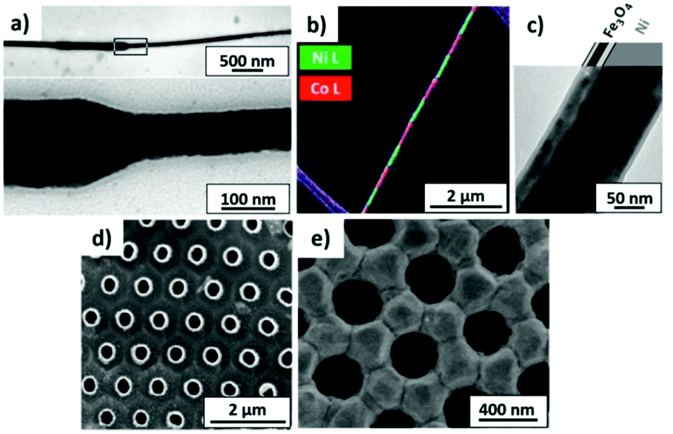 | ||
| Fig. 17 (a) Transmission electron (TEM) micrographs of a single modulated Ni wire isolated from the alumina template. Top, low magnification image showing two diameter changes. The area defined by the rectangle is further magnified in the lower panel. Reprinted with permission from ref. 258. Copyright © 2011, AIP Publishing. (b) EFTEM (energy-filtered transmission electron microscopy) image of a multisegmented Co/Ni nanowire. Reprinted with permission from ref. 38. Copyright © 2016, the American Chemical Society. (c) TEM image of an Fe3O4 (outer)/Ni (inner) core-shell nanowire. Reprinted with permission from ref. 259. Copyright © 2010 WILEY–VCH Verlag GmbH & Co. KGaA, Weinheim. (d) SEM top view image of an array of hollowed carbon nanotubes (CNTs) grown inside the porous structure of an alumina template through a CVD deposition process. Reprinted with permission from ref. 46. Copyright © 2017, the American Chemical Society. (e) SEM image of sputtered Si0.8Ge0.2 nano-mesh film grown over an alumina template, where the porous structure was successfully replicated. Reprinted with permission from ref. 66. Copyright © 2016, Springer Nature. | ||
This method has been extensively used for the fabrication of magnetic nanowires as a way to increase the density storage and performance of already existing magnetic recording devices such as RAMs and hard drive disks due to their high-aspect-ratio or for the development of some new racetrack memories247 and design of future magnetic logic devices248–251 through tunning of the magnetic anisotropy governing the magnetic behavior behind the nanowires. As their dimension is reduced along at least one space direction (diameter or length of the nanowires), shape anisotropy becomes dominant over the other the magnetic forces contributing to the total magnetic anisotropy energy. Moreover, due to space confinement, control over the magnetization and demagnetization process, as a consequence of controlling the domain wall motion along the nanowires, can be achieved.252,253 Different types of domain walls have been reported, separating different magnetic domains (in which spins are aligned in the same direction), depending on the diameter of the nanowires. In general, for diameters below 40 nm, the formation of a transverse domain wall (TDW) is favored, which is a high energetic configuration in which spins rotate transversely to the nanowire length and is favored due to strict space limitations. In contrast, a vortex domain wall (VDW) configuration is found in nanowires with diameters bigger than 40 nm, where changes in the magnetization undergo a less energetic curling process of the spins from one direction to the opposite one, moving along the nanowire length.252,254–256 These numbers can change depending on the magnetic material.252 The racetrack memories first proposed by IBM were designed to exploit the control over domain wall motion in nanowires by the injection of an electric current.257 More sophisticated and recent studies specifically combine both types of domain wall configurations to gain more precise control over the magnetic response by the generation of well-defined pinning sites in the development of more complex logic devices, where the control over the position and motion of domain walls is the key factor. This can be achieved through modulation of the pore diameter along the length of the fabricated nanowires37,39,249,251,258 (see Fig. 17a).
Also, tuning of the magnetocrystalline energy adds an even higher degree of control over the magnetic properties and domain wall motion by tailoring the chemical composition of magnetic nanowires36,260,261 and multilayered36–38,262,263 or even core-shell nanowires259,264 through alloying (as shown in Fig. 17b and c, respectively).
A rather interesting phenomenon, giant magnetoresistance (GMR), has also been experimentally observed in multilayered nanowires due to the spin transfer process between adjoining layers of hard and soft magnetization, which occurs through an exchange coupling mechanism.265,266 GMR is displayed in multilayered systems where two possible spin-channels exist, which is associated with a maximum resistance state (antiferromagnetic coupling between subsequent layers) or a minimum resistance (ferromagnetic coupling). Switching between the antiparallel (high resistance) and parallel (low resistance) states is propelled by an external magnetic field. This effect can be directly employed in the fabrication of spin-valve sensors and magnetoresistive random-access memories (MRAM).
It is also worth mentioning the use of these magnetic nanowires, in particular core-shell structured nanowires, in biomedical applications267 for cell separation268,269 and tracking,270 as drug delivery vehicles driven by a magnetic field and hyperthermia treatment.271
Another important application of nanoporous alumina membranes as templates for the fabrication of nanowires is in the field of thermoelectric materials (such as bismuth telluride272,273), which convert waste heat in the form of a temperature gradient into usable electricity. In 1993, Dresselhaus274 first predicted the enhancement of the thermoelectric performance of these materials when reducing their dimensions, for instance, in the form of 1D nanowires. The efficiency of a thermoelectric material is defined by the dimensionless figure of merit, zT = S2σ/κ, where S is the Seebeck coefficient, which measures the generated voltage due to an induced temperature gradient across the material (ΔV/ΔT), while σ and κ are the electrical and thermal conductivity, respectively. These three parameters are deeply intertwined, and thus if S increases, σ decreases, and increasing σ increases κ (as a result of the increase in the electron contribution to the total thermal conductivity), and thus effective enhancement of zT cannot be achieved this way. Nanowire engineering aims to decouple these parameters to obtain phonon-glass electron-crystal behavior, as theoretically proposed by Dresselhaus in 1D quantum wire structures.274,275 In this case, the electron conductivity is enhanced along the length of the wire through free electron motion in this direction (transition from semimetal to semi-conductor behavior243) and phonon scattering is increased in the direction perpendicular to that due to the presence of the surface of the nanowires, which reduces the thermal conductivity.276 This can be achieved since normally both electrons and phonons suffer collision events or scattering processes at significantly different characteristic distances. Specifically, in most materials, the mean free path of phonons (in the range of hundred nanometers) is higher than that of electrons (usually in the order of tens of nanometers), and therefore the scattering of phonons with the surface of the nanowires increases their scattering without affecting the electrons. Furthermore, the Seebeck coefficient can be further improved due to the increase in the density of states at the Fermi level as a result of the reduction of the dimensionality. Nevertheless, the diameters required to experimentally observe an enhancement in S are too small for most of the interesting materials and is below the lower limit that can be achieved through AAO-based technology (i.e., to fulfil this requirement, bismuth telluride nanowires with diameters of 1 nm are needed). Still, it is possible to use nanowire structures of thermoelectric materials employing alumina membranes as templates to improve their thermoelectric figure of merit, zT, through an increase in σ or a reduction inf κ. In particular, the latter approach has yielded more successful results to date. Other effects, besides the increase of phonon boundary scattering commented before, such as topological insulator effects associated with the appearance of surface electron states, among others, have been experimentally found in low-dimensional structures such as nanowires fabricated inside alumina templates.27,28,246,277 These effects have provided some of the latest breakthroughs in the field of thermoelectricity, both from experimental and theoretical points of view.
A different synthetic route has also been reported for the fabrication of nanowires using AAO membranes as templates. In the case of SiC core-shell nanowires, it has been discovered that if plasma deposition is performed, the deposited material, does not grow along with the pores, and hence, filling of the pores does not occur. Instead, a different growth mechanism is involved. Since the porous surface of the alumina membrane has some texture with crests and valleys, corresponding to the triple union point of the walls of adjacent pores and the actual nano-pores, respectively, nucleation of the SiC nanowires is promoted at the crest points. At these sites, plasma-induced reduction of the aluminium oxide to metallic Al occurs and Al droplets are formed, where later Si and C atoms will be incorporated by the plasma process through Si/C co-precipitation. Subsequently, nanowire growth occurs, thus resulting in the formation of core-shell nanowires made of an SiC core and an AlSiC outer shell.29
Another approach is the use of alumina membranes as templates to produce long-range nanostructured surfaces with antireflective qualities, which are especially important for solar cell applications, to reduce the reflected light at the film-air interface as light travels from one medium (air) to another (material film) with significantly different refractive indexes. They are normally used as a mask during the plasma etching process or in nanoimprint lithography to produced periodic Si nanopillar arrays.30,278–280
Al nanomeshes have been proposed as transparent conductive Al electrodes for third-generation optoelectronic devices of LEDs, photovoltaics, touchscreens, etc., where besides fulfilling the actual requirements of low resistance and high light transmission, low-cost production, and increase in their flexibility are desirable. Through an easy and cheap anodization process of a sputtered aluminium layer over a glass slide used as a substrate, followed by a controlled chemical etching step, the alumina membranes are removed, leaving only the non-oxidized sputtered aluminium with a patterned structure. Consequently, Al nanomeshes were obtained with increased optical transparency above 70% due to the presence of nano-holes.296
In the field of thermoelectricity mentioned above, several studies have been carried out on the thermal transport mechanisms behind this type of perforated film.66,67 A significant thermal reduction was observed as the distance between holes (w) was reduced due to enhanced phonon-surface scattering events, and in-plane confinement was promoted by the presence of holes.297,298 In these systems, the electrical conductivity was slightly degraded; however, the overall thermoelectric performance of the nanomeshes was improved in comparison with that of continuous films. If further optimization of the electrical conductivity is achieved, these holey films can easily compete with nanowire technology due to the higher mechanical strength of the former, which makes its integration into TE modules much easier.
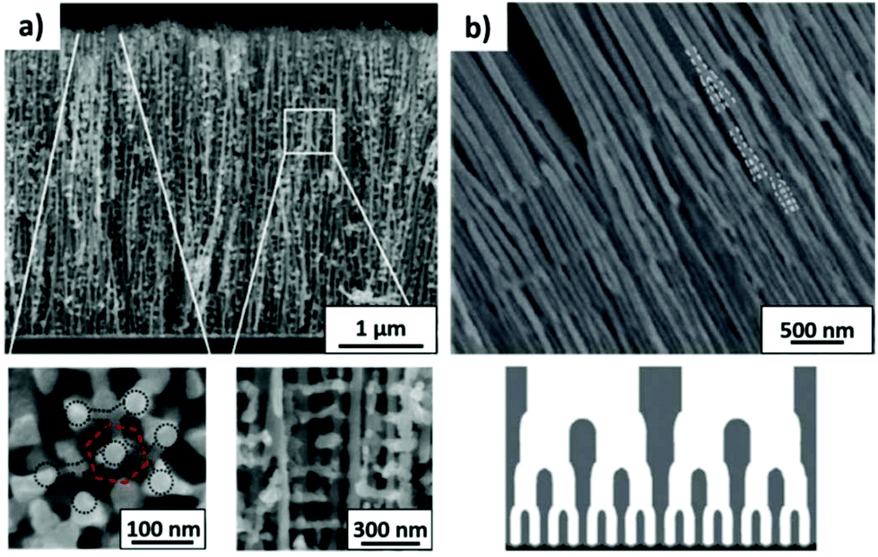 | ||
| Fig. 18 (a) SEM cross-sectional image of a 3D Ni nanowire network after removal of the alumina template, underneath the top view (left) and cross-section (right) of the nano-network structure at high magnification. The dashed red lines represent the unit cell of the alumina template of hexagonal pores arrangement. Reprinted with permission from ref. 57. Copyright © 2018, the American Chemical Society. (b) SEM image of Ni nanowires with three-generation Y-branched morphology. Bottom: schematic drawing of such multi-branched nanowires. Reprinted with permission from ref. 53. Copyright © 2010 WILEY-VCH Verlag GmbH & Co. KGaA, Weinheim. | ||
Some recent examples have been developed in the case of metal nanostructuring since they can be applied in the electrolytic production of hydrogen, where their high surface area and high porosity are optimal for this application,57 as shown in Fig. 18a. This advantage should be also relevant for applications in battery electrodes, and therefore V2O5 has been grown through a template-assisted deposition process in these types of 3D AAOs. Nevertheless, in this case, the obtained results showed that the performance was not improved, but diminished due to the negative effect of the interconnections on the final capacity and the poor electronic conductivity of the material.58 Another interesting possibility when using these 3D AAOs as templates is filling them with magnetic materials, such as Ni26,59 and Co.59 By tailoring the nanostructure, the magnetic anisotropy of the whole system can be modified, obtaining properties that are different from both magnetic nanowires and magnetic thin films.59
Also, in the case of thermoelectric applications, 3D nanowire networks fabricated via template-assisted deposition provide a great advantage over thermoelectric nanowires, which is the possibility of having the improved properties that the nanostructuring provides together with a mechanically stable structure at the macroscale, which can be easily handled. For instance, thermoelectric materials such as bismuth telluride have been already synthesized in this form60 and the main advantage of nanostructuration, that is, the reduction in i thermal conductivity, is maintained.299
Branched nanowires (Nws), branched nanotubes (NTs) and a segmented hybrid combination of Nws-NTs with a branched structure can also be considered as another type of 3D nano-architectures,50,300 where, again, the enhancement of the available surface area is of great relevance for applications such as energy storage and solar cells due to the improved light absorption in these structures, as shown in ref. 301. Moreover, the electronic transport properties of Y-branched nanowires have also been an object of study of different materials, ranging from CNT51,302 (see section 6.3.1) to solid Bi52 branched nanowires. The magnetic behavior of a single Y-junction of Ni nanowires was investigated by Guo et al.303 Also, more complex multi-branched structures made of different materials (Si-NT/Nw, Au, Ni, Ge-NT/Nw, and Pt), as shown in Fig. 18b, have been synthesized with potential applications in nanoelectronics,53 in particular, for the development of improved transistors, as in the case of Y-branched nanotubes/nanowires based on Ge,54 nanomagnetism53 and for catalytic applications.55
6.2 Template-assisted fabrication of organic nanostructures
Recently, these structures have demonstrated their applicability for transport46 and sensing326 of certain molecules, and CNTs with modulated diameters along their length can be implemented for the filtration and separation of molecules, cells, or proteins.327
Some of the most notable applications of nanostructured polymers are in the development of future biosensing, electronic, and optoelectronic devices. For example, improved luminescence and lasing properties were reported due to the preferred orientation of the β-phase polymer chains along the nanowire axis in PFO nanowires and nanotubes.32,332 Later, the same researchers demonstrated the possibility of controlling the polarization direction of PFO light emission in the form of Y-branched nanowires by adjusting the angle between branches.333 Several studies on the electrical transport properties of polymeric PEDOT nanowires,31,47 and PH3T nanotubes48,334 showed improved carrier mobility and electrical conductivity, respectively, which are qualities required for the fabrication of organic field-effect transistors and solar cells. 3D polymeric membranes, as mentioned above, with a Bragg reflector photonic response, are good candidates for chemical and biosensing applications. Further functionalization of the surface of polymeric nanowires can enhance their selectivity and sensibility for the detection of specific molecules, or make them responsive to certain stimuli (such as pH, humidity, and light).56
7 Properties of nanoporous anodic alumina structures and their applications
Nanoporous alumina is widely used in different fields. Obtaining a self-ordered highly porous structure is important, for instance for increasing the adsorption and the fabrication of membranes. Moreover, the great control over the diameter of the pores, together with the long-range self-ordering can be used to generate structural coloring by different means, and the high surface to volume ratio of these porous structures can be also used for biosensors once the pore walls have been activated with certain substances. Next, we will review some of these applications.7.1 Structural coloration
The sole presence of a patterned nanostructure with a certain order produces a bright structural coloration on metallic surfaces, which is angle sensitive. This coloration is produced by the interference of light with the ordered patterned structure, as shown in ref. 8. Ordered dimple arrays with a diameter of 500–550 nm were produced on an aluminium substrate during anodization in phosphoacetic acid. After the chemical dissolution of the oxide layer, structural coloration was observed in the visible range of 500–700 nm, coming from the reflected light on the periodically ordered dimple array over the aluminium surface.The structural coloration of nanoporous alumina membranes is mostly based on the Fabry–Perot interference occurring at the Al metal/AAO film and air/AAO film interfaces (see section 7.2 for a more detailed description of this effect); however, there is a threshold thickness of around 2 μm, above which, this interference is not observed342 since all the incident light will be absorbed by the porous membrane. Regardless of the film thickness limitation, the way light interferes at the different interfaces can still be modulated to produce coloration with a high degree of tunability by two means, namely controlling the depth of the pore channels (or a total thickness of the oxide layer within the limiting range)343,344 and by tuning the porosity (changing the pore diameter or interpore distance while one of the two is fixed)341,345 since both structural features produce changes in the effective refractive index of the anodic aluminium layer. Using all these different parameters, virtually any structural color can be produced with these structures according to Bragg's law.
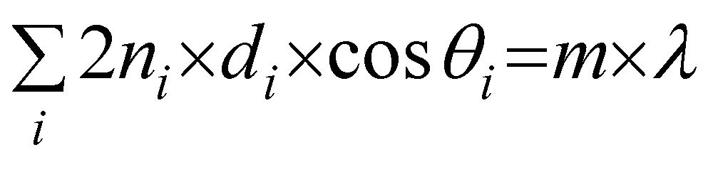 | (11) |
This establishes a clear relationship between the effective refractive index and the reflection of light, and hence the colours that are perceived, where ni is the effective refractive index, di is the thickness, θi is the reflection angle, m is the order number and λ is the reflective peak wavelength that gives the observed colour. The suffix i stands for the different dielectric layers with different refractive indexes of which the alumina membrane can be composed (see section 5). It is also worth mentioning that the latter two parameters, and thus the structural coloration, are angle-dependent on the incident light.
Moreover, the deposition of a metallic layer over the nanoporous AAO can further improve the colorimetric response of these membranes, adding a higher variety of colors, as well as enhancing the reflectance of the light on the metalized surface. In 2018, Manzano et al.341 studied the dependence of the different structural parameters of AAO films (interpore distance, pore diameter, porosity, the thickness of the oxide layer, and chemical composition as a function of the anodizing electrolyte) against coloration and the effective reflective index of the films. According to their experimental observations, the authors concluded that the thickness and porosity of the AAO films are the only two morphological parameters that influence the effective refractive index of the films, thus affecting their color. Fig. 19a clearly shows the inverse relationship between the values of the effective refractive index and the thickness of the alumina membrane. The porosity of the films also affects both the refractive index and coloration, as is seen when comparing samples grown in oxalic acid and that anodized in sulfuric acid and ethylene glycol mixed electrolyte solution, which showed a similar porosity of 13.2% and 13.6%, respectively. Thus, alumina films with the same porosity, also having the same thickness, show nearly the same coloration. However, when the porosity was significantly reduced to 11.5% (samples anodized in sulfuric acid, red line), a different coloration was obtained when fixing the thickness. For example, an AAO film with a thickness of around 800 nm showed a vibrant green coloration in sulfuric acid-containing ethylene glycol solution (green line) compared to the light blue color of the alumina film of the same thickness when it was anodized in sulfuric acid. To further prove this dependence, other morphological parameters were varied such as pore diameter and interpore distance, while the thickness and porosity of the alumina films were fixed. Accordingly, two different sets of samples were grown (Fig. 19b and c) with the same coloration. A golden hue was achieved when the thickness and porosity of the films were fixed at 437–435 nm and 13.6–13.2%, respectively. The corresponding refractive index was around 2, regardless of the other structural parameters such as pore diameter and interpore distance, which were both varied by changing the electrolytic medium, using in each case oxalic acid and sulfuric acid-containing ethylene glycol. Another pair of green-colored AAO films were grown in oxalic (pore diameter 30 nm and interpore distance 100 nm) and sulfuric acid (pore diameter 20–25 nm and interpore distance 62–65 nm) with fixed thicknesses of 935 and 938 nm and porosities of 13.6% and 11.5%, respectively. The effective refractive index of the samples was in the range of 1.4–1.3, giving a final green coloration. In this study, all the samples were metalized with a thin layer of Cr to enhance the colorimetric response of the anodic oxide films. An optimized layer thickness of 8 nm was used considering that the thickness of the evaporated metallic layer must be thin enough to avoid the propagation of light in the metal but not too thin that the absorption of light is not enhanced.
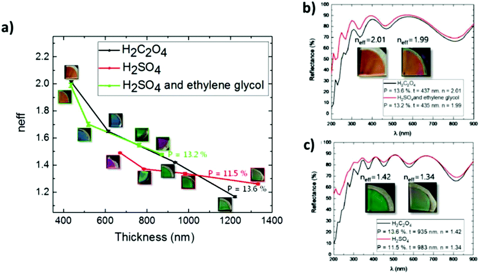 | ||
| Fig. 19 (a) Effective refractive index as a function of the thickness for different percentages of porosity (achieved by varying the anodization conditions and electrolyte solution) and the corresponding optical images of the fabricated Cr–AAO–Al films. (b) and (c) UV-Vis reflectance spectra of AAO–Al films anodized in different electrolytes while the thickness and porosity were kept constant. Inset shows optical images of the films. Reprinted with permission from ref. 341. Copyright © 2018, the American Chemical Society. | ||
Previous works have investigated this mechanism, where the interaction between light and the porous structure of AAO films was improved by the addition of a metallic layer. In the simplest case of an AAO film, phase modulation of the light in the porous structure generated a wavy profile, where reflective peaks appeared at wavelengths corresponding to the in-phase interference of light (constructive interference), while valleys were formed when the phase difference between the reflected light at the two different interfaces was out of phase (destructive interference). By adding a thin metal layer, the maximum absorption of light should occur at the wavelengths associated with the destructive interference (valleys) of light in the anodic oxide film, and thus the reflective profile of the valleys is sharpened. In this conjugated twin-phase mechanism, which was proposed by Xue et al.,345 constructive and destructive interference in the metal layer conversely correspond to that of destructive and constructive interference in the AAO film. The thickness of the top metal layer was designed so that asymmetric phase modulation between the two layers is achieved, hence improving color saturation. Further enhancement of the reflective peaks was accomplished by increasing the roughness of the metal layer, which led to an increase in the broad band absorption efficiency of the film.
The authors developed a color printing technique combining the color saturation approach described above together with full-color generation through tuning the thickness and porosity of the AAO layer with lithography in such a way that a pattern could be written over the metal-AAO-Al films and then revealed by simple chemical etching (Fig. 20a). The colors of the pattern could be selected by adjusting the thickness and etching time of the anodic oxide layer (through a change of the porosity and effective thickness between the patterned and unpatterned AAO regions). Furthermore, by carefully choosing colors that appear in a narrow wavelength range, the pattern could be encrypted. In Fig. 20b, encryption of the pattern was achieved by first selecting blue and green as contrasting patterned colors with corresponding reflective peaks lying in close wavelength numbers. Then, when coated with poly(methyl methacrylate) the refractive index of the AAO changed, producing a red shift in the whole reflectance spectrum of the sample. After the red shift, both colors were located in the green region, and thus the encrypted pattern became invisible. When the polymeric layer was removed, the patterned code could be read once again. These experiments demonstrated the viability of using structural coloration of AAO for writing and labeling applications, as well as anti-counterfeiting and data encryption storage applications with a small micrometric resolution on large sample areas up to the centimeter scale.
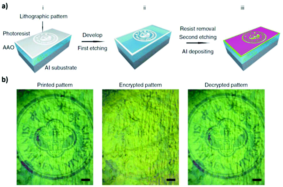 | ||
| Fig. 20 (a) Method of colour pattern printing. (i) After spin-coating on an AAO template, the photoresist is patterned using photolithography. (ii) The photoresist is developed to leave the designed patterns, after which the first acid etching is implemented to form the difference of effective thickness of the AAO template (and thus a difference in the effective refractive index) between patterned and unpatterned AAO domains. (iii) An Al layer is sputtered on the sample to form the designed colourful pattern after the removal of the photoresist and the implementation of the second etching. (b) Encryption of the printing pattern by choosing colors with a small wavelength difference. The image on the left, printing pattern in blue color, and green-black ground (printed pattern). Both colors are within close wavelengths numbers. The image in the center, spin coating of PMMA produces a redshift in color and the pattern becomes invisible (encrypted pattern). Blue color shifts towards green. Right image, after removal of the PMMA layer, the pattern becomes clear again (decrypted pattern). Reprinted with permission from ref. 345. Copyright © 2015, Springer Nature. | ||
In the case of nanoporous structures with non-homogeneous diameters along the depth of the pores (modulated nanopores,346,347 or even 3D nano-structures348), the oscillatory optical response of these structures is based on the interference of light reflected through a multilayer nanoporous structure of alternating layers of low porosity (MA layers) and high porosity (HA layers) with higher and lower refractive indexes, respectively (see Fig. 21b). High porosity layers correspond to wider pore segments (see Fig. 11d or Fig. 12 in section 5.2) in the case of modulated nanopores. Regarding 3D porous structures, high porosity layers are associated with the transversal nanochannels interconnecting the longitudinal pores (see Fig. 13, section 5.3 and Fig. 21a, section 7.1) with a porosity that can reach up to 80% compared to the longitudinal pores of around 20% porosity (low porosity layer). Thus, the refractive index of each layer is defined by the fraction of alumina filled by air and changes as a function of the corresponding porosity. Fig. 21b illustrates the periodic modulation of the refractive index through the 3D alumina membrane and reflection of the light between adjacent layers.
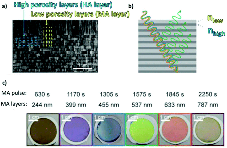 | ||
| Fig. 21 (a) Cross-sectional SEM image of AAO membrane, where HA layers are identified in blue and MA layers are marked in yellow. (b) Schematic of the interaction of light at the different layers of higher (nhigh) and lower (nlow) refractive indices associated with high porosity and low porosity layers, respectively, behaving as a Bragg stack. (c) 3D-AAO Brag reflectors with a pre-designed reflectance by the thickness of MA stack layers. Reprinted with permission from ref. 61. Copyright © 2018 WILEY-VCH Verlag GmbH & Co. KGaA, Weinheim. | ||
Considering that the fabrication method allows great control over the thickness of each of these layers, as well as its periodicity, one can fabricate a periodic structure combining different layers, and thus a distributed Bragg reflector is obtained, where propagation of specific wavelengths can be designed to produce the desired coloration of the fabricated membrane. Fig. 21c shows different Brag reflectors specifically designed to have a certain colorimetric response as a function of the thickness of the low porosity layer (MA layer), which can be controlled by the duration of the MA pulses.
This type of physical coloration through nano-engineering of the structural parameters is also presented in nature, ranging from opals to butterfly wings (see, for instance, ref. 61 and 348).
In all the different approaches used to modulate the color of AAO membranes from metal-AAO-Al films to MA/HA multilayered AAO, due to the porous nature of these anodic oxide membranes, the refractive index of the initial metamaterial composed of a porous alumina structure filled by air will be drastically changed by wetting in water (or any other liquid or gas) since the propagation of light changes as a function of the surrounding medium. This change in the effective refractive index results in a shift in the reflection peaks, and hence different colorimetric responses due to environmental changes. This process is reversible, and therefore it can be easily implemented for the fabrication of colorimetric sensors to detect certain substances.61,349
Another property of these structures is that their color changes depending on the substrate on which they are placed. A specific example of this property of color sensitivity is provided in Fig. 22. This 3D AAO structure, after removal of the remaining Al substrate, was completely transparent, but when placed on different substrates the same sample exhibited a significant color variation. Light will be first reflected from the substrate located underneath the 3D-AAO membrane and then propagates back through the metamaterial, and thus a change of color is observed depending on the nature of the substrate. Fig. 22 shows a clear change in the perceived color from green to pink when the 3D-AAO membrane was placed on top of a lighter or a darker substrate. In the former, most of the light is reflected and will propagate back, while in the latter case, light is only partly reflected since most of it will be absorbed on the dark background, resulting in the observed change of coloration. These features, both the dependence of the substance filling the pores and the substrate used, can be specifically used for security, anti-counterfeiting, camouflage detection, and food safety applications, as cited by the authors.
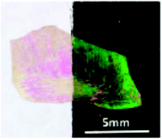 | ||
| Fig. 22 Observed color change of the 3D-AAO sample from pink to green when placed on top of different substrates. Reprinted with permission from ref. 348. Copyright © 2018, the American Chemical Society. | ||
7.2 Optical and photonic crystals
The fabrication of photonic crystals based on anodic alumina templates is a step forward in the control and modulation of light. Lately, there has been a great development of these structures based on nanoporous anodic alumina, mainly because this method presents several advantages compared others to produce photonic crystals, being cost-competitive, fully scalable, and relatively simple to implement. An extensive review of a wide variety of structures fabricated up to 2017–2018 can be found in ref. 350 and 351The pioneering work of Masuda and coworkers demonstrated the feasibility of the structural engineering of nanoporous alumina for the fabrication of 2D photonic crystals. By exploding the tunability of the effective medium of these membranes, which can be treated as a composite material consisting of an alumina matrix filled by air, one can control the way light is propagated across the porous AAO structure, as established by the Bragg eqn (11). Masuda et al.352 reported the modulation of the position at which a photonic bandgap appears, where by controlling the interpore distance in the alumina membrane, a red shift was observed as the cell size (interpore distance) increased. Further control over the position of this photonic bandgap could be achieved by the widening of the pores through chemical etching, while the interpore distance was kept constant. In this case, a blue shift of the photonic emission was recorded.
Accordingly, the development of more complex anodization processes to gain control over the in-depth modulation of the porous structure of alumina such as pulsed and cyclic anodization techniques has monopolized most of the attention of researchers. Hence, most of the examples of photonic crystal structures found in the literature are based on branched, modulated, or 3D-nanoporous anodic alumina.
According to what has been stated up to this point, 4 different morphologies with which alumina membranes have been fabricated through nano-engineering of their structural parameters (and thus engineering of the effective medium and generating photonic crystal structures) can be highlighted (see Fig. 23).
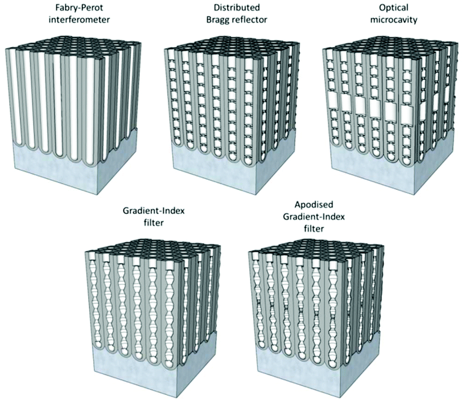 | ||
| Fig. 23 Structural details of the photonic crystal structures made from nanoporous AAO membranes by structural engineering of the effective medium. | ||
Recently, their performance as chemical sensing platforms was tested by Ferro et al.14 in a study evaluating the Fabry–Perot interference spectra of AAO films as a function of glucose concentration through photoluminescence measurements, combined with other multivariate analytical data processing techniques. The determination of glucose concentration with good analytical performance was reported employing this approach.
However, these proposals based on straight pore channels were shown to have geometric limiting factors (limiting the range of the structural parameters with which alumina membranes can be fabricated, including interpore distance, pore diameter, porosity, and thickness) and therefore, their versatility is too low for most practical applications.
 (within MA regimen), an n-branched porous alumina structure is formed, as described in section 5.1. However, as the voltage is periodically restored to VH, only one of the branched channels will continue to grow to undergo a new branching process, while the others will be terminated at this stage (as shown in the SEM image and schematic drawing in Fig. 24b).
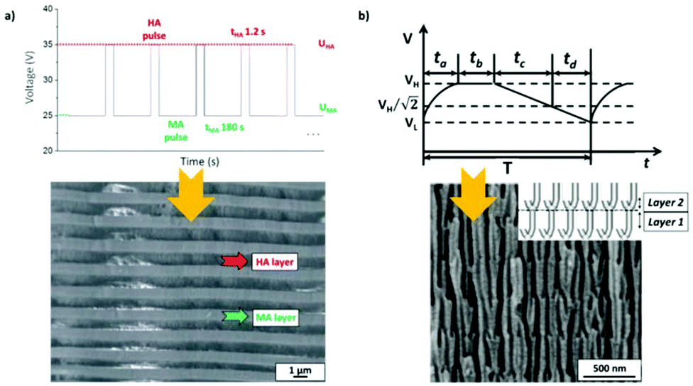 | ||
| Fig. 24 (a) Typical voltage signal applied during the pulse anodization of aluminium, where UMA and UHA are the anodizing potentials used to achieve mild anodizing (MA) and hard anodizing (HA) conditions, respectively. Bottom, cross-sectional view of the resulting stacked Bragg-based alumina structure with alternating MA and HA layers formed by pulse anodization in 0.3 M sulfuric acid at 1 °C, after selective etching (in 0.52 M phosphoric acid at 45 °C for 20 min) of the HA layers. Reprinted with permission from ref. 211. Copyright © 2011 Elsevier Ltd. All rights reserved. (b) Applied voltage signal profile during pulse anodization under MA conditions in 0.3 M oxalic acid. Bottom, scheme of the resulting photonic crystal heterostructures composed of two different photonic crystals with different lattice constants (PC1 and PC2). Reprinted with permission from ref. 353. Copyright © 2008 Elsevier B.V. | ||
The typical voltage signal profile of pulsed anodization in the MA regimen is illustrated in Fig. 24b, where two well-defined segments of different trends can be identified, namely sinusoidal increase in the applied potential to VH and a linear decreasing segment down to VL, where both segments are periodically repeated during N cycles. The stacked branched porous alumina is characterized by two main layers, where layer 1 is the main stem pore corresponding to the periods between ta to tc, with a characteristic d1 thickness and n1 refractive index. Also, layer 2 consists of branched smaller pores formed during time td, with a d2 layer thickness and n2 refractive index. Then, according to the Bragg reflection law (7), varying d1/n1 or/and d2/n2 of each respective layer, the locations of the photonic bandgaps can be tunned across the UV-VIS-NIR spectrum354 depending on the desired applications. Generally, a red shift (towards higher wavelengths) as tc is increased has been reported,353,355 while pore widening produces a blue shift.349,356,357
The fabrication of stacked photonic heterostructures, PC1, and PC2, that generate two different (first-order) photonic band gaps has also been reported.355,358 In particular, overlapped, staggered, and split photonic bandgaps were generated by tuning the location of the first order photonic band of PC2 along the UV-VIS spectrum with an increase in the anodization voltage.355
Overlapping of several band gaps can be directly applied to produce a huge prohibited photonic bandgap as a way to reduce reflection losses in dielectric materials. Moreover, the separation between splitting bandgaps can be tuned for filtering applications, with control over permitted passbands and multichannel transmissions.
Photonic crystal heterostructures based on 3D porous alumina networks, where the periodicity of the high and low porosity layer (layers of low and high refractive index, respectively) is systematically altered as the thickness of such layers is gradually reduced, have been proven to enhance the optical sensibility four-fold (translated into a change of color) due to induced resonant interference.16
Additionally, the high control that the abovementioned Bragg reflector-AAO structures have demonstrated to provide fine adjustment of the location of the optical bandgaps can be used to make them sensitive to specific changes in the effective media inside the nanopores. A redshift in the photonic stopband of porous alumina photonic crystals has been experimentally observed based on the distributed Bragg reflector structures described above and a decrease in the intensity in the transmission spectra with exposure time and increasing concentration of different substances from liquids (of increasing refractive indexes water, ethyl alcohol, ethylene glycol, and glycerol, for instance)359 to gases (ethanol, methanol, acetone and toluene.360,361 Based on this sensitivity towards changes in the effective medium, more sophisticated BR-AAO sensors have been developed for the detection of specific molecules, such as vitamin C362 or particles, such as mercury ions, Hg2+.17
Accordingly, Wang et al.363 developed two different types of optical microcavities, type I and type II, as shown in Fig. 25. If both N cycles of pulsed anodization to form the AAO Bragg reflectors are applied in-phase, or if a phase shift is introduced between them without the need for a central microcavity, then constructive or destructive interference is promoted at certain wavelengths, respectively. In type I, the resonance peaks are introduced in the photonic bandgap of in-phase (constructive interference) distributed Bragg reflectors at each side of a central cavity layer with a constant refractive index according to the Bragg condition for constructive interference, nHdH = λ/4 = nLdL, where nH, dH and nL, dL are the refractive indexes and thicknesses of the grown layers under high and low voltage, respectively. By optimizing the length of the resonant cavity, resonant peaks appeared at positions corresponding to the different order resonant peaks associated with the Bragg reflector structure. To produce type II, a phase shift from 1/2π to 7/4π was introduced between the two Bragg reflectors to achieve destructive interference, which translates into a shift in the refractive index of the bottom distributed Bragg reflector (DBR) structure. However, resonant first-order peaks only appeared for a 7/4π phase shift or higher. At lower phase shifts, significant structural changes were not observed at the interface, in other words, no modulation of the pore geometry occurred. The authors hypothesized that these low phase shifts are associated with an early stage in time as the voltage is reduced from VH to VL, at which a steady current state has not yet been reached. Thus, modulation of the pore shape does not occur, and therefore there are no changes in the refractive index. This is one of the major drawbacks of this method, as previously mentioned in section 5.1, because as the voltage is reduced during the formation of branched pores, relatively long recovery times are needed until the new steady state is reached, and thus the formation of pores is also delayed. Changes in the pore structure can be observed once the steady state is achieved, that is, after thinning of the barrier layer down to the corresponding value of the low anodization potential, VL.
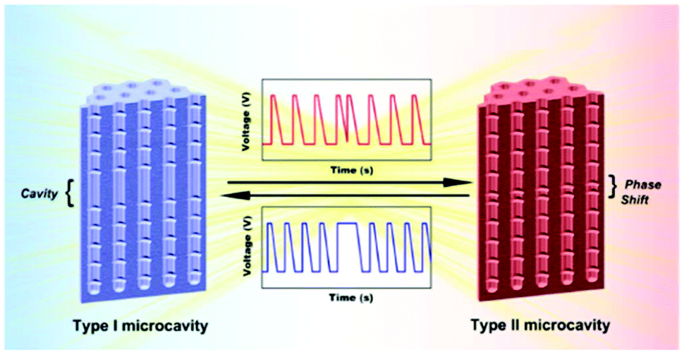 | ||
| Fig. 25 Illustration of the fabrication process of AAO microcavities by pulse anodization. Type I microcavities are prepared by inserting a cavity layer between the AAO-DBR structures (left side in blue). Type II microcavities are fabricated by shifting the phase of anodization to achieve the phase modulation of an effective refractive index in the bottom Bragg reflector structure (right side in red). Reprinted with permission from ref. 363. Copyright © 2015, the American Chemical Society. | ||
Both types of microcavities offer great versatility in the way that resonant peaks and stop bands are tuned across the UV-visible and near-infrared spectra. Moreover, the specifically added resonant peaks are narrower and the energy transmission of these peaks is enhanced compared to the actual photonic stop bands of the distributed Bragg reflectors, and thus the performance (higher sensitivity and quality factor, Q ref) of these photonic structures is improved.16,363,364 Combining the improved photonic response of the aforementioned type II microcavities, together with the intrinsic dependence of Bragg reflectors to the effective medium, the authors developed a humidity sensor.363
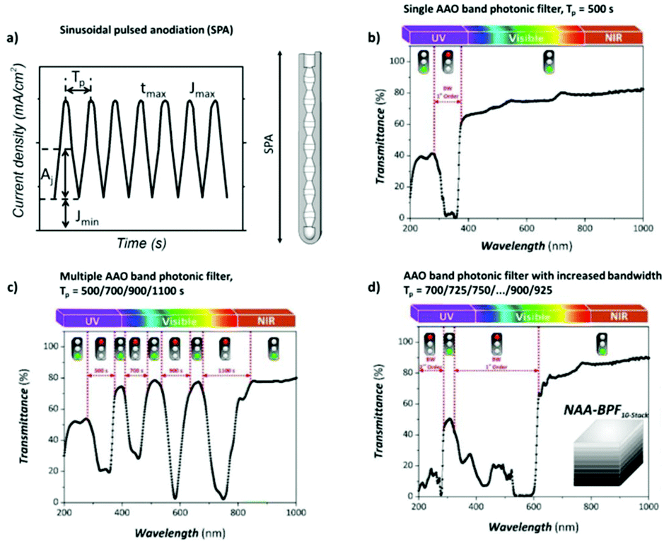 | ||
| Fig. 26 (a) Typical applied current profile during the fabrication of porous alumina optical filters and graphical description of the anodization parameters (Tp = anodization period, Aj = anodization amplitude, Jmin = minimum current density, Jmax = maximum current density, tmin = time at Jmin, and tmax = time at Jmax) to the left. Right, illustration establishing the correlation between the profile of the applied current curve and the final pore geometry of the AAO membrane. Reprinted with permission from ref. 364. Copyright © 2018 The Royal Society of Chemistry. (b) Transmission spectrum of a single AAO band photonic filter with characteristic stop band at 331 nm associated with Tp = 500 s. (c) Transmission spectra of multiple AAO band photonic structure filters with designed stopbands at an anodizing time of 500 s, 700 s, 900 s, and 1100 s. (d) Transmission spectra of an AAO band photonic filter with huge bandwidth by increasing the anodization period in increments of 25 s, from 700s to 925 s. Reprinted with permission from ref. 366. Copyright © 2016 The Royal Society of Chemistry. | ||
These gradient-index filters have proved to be useful for sensing applications.16,368,369 Several studies show that engineering of the porous alumina structure can improve its sensibility to certain molecules (i.e., detection of different concentration levels of D-glucose, where the sensibility of the GIF structure towards changes in the refractive index was enhanced, the detention limit of 4.93 nm M−1 was reduced to 0.01 M).368 Moreover, the functionalization of the alumina surface further improves the sensing capability of the alumina gradient filters. For example, thiol-modified surface AAO-GIFs were developed with increased sensibility to Hg2+.369 Using more complex functionalizing agents such as amino acids or proteins, more complex detection systems for vitamins and drugs370,371 were designed.
Another interesting application making use of more complex AAO-GIFs systems with tuned located narrow peaks through multiple-sinusoidal anodization (MSPA, consisting of the combination of multiple sinusoidal waves) was proposed by Santos et al. for optical encoding of information within the porous alumina structure based on a color barcode system.367 They fabricated an 8-bit encoding system with ON(1) and OFF(0) states by enabling or suppressing certain transmission peaks through modulation of the depth of the pore channels. Additionally, each of the different possible combinations of ON/OFF states was associated with a specific interferometric colour. The developed color barcode encoding system is shown in Fig. 27.
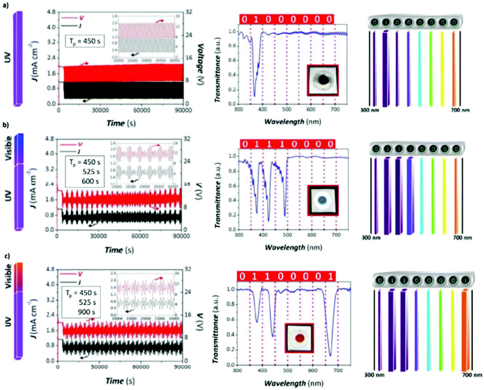 | ||
| Fig. 27 Generation of an 8-bit encoding system in AAO-GIF photonic crystal structures by MSPA. Left, multiple sinusoidal applied waveforms (inset shows a magnified view of the anodizing profiles). Center transmission spectrum (inset image interferometric color response of the photonic crystal structure) and right photonic bar code. Corresponding to (a) AAO-GIF photonic crystal structure with code 01000000 (number of waves ON = 1, Tp = 400 s) and (b) AAO-GIF photonic crystal structure with code 01110000 (number of waves ON = 3, Tp = 400, 525, and 600 s). (c) AAO-GIF photonic crystal structure with code 01100001 (number of waves ON = 3, Tp = 400, 525, and 900 s). Reprinted with permission from ref. 367. Copyright © 2016 The Royal Society of Chemistry. | ||
A different application of alumina porous membranes with gradient refractive index structures is the development of anti-reflective films. In this case, the refractive index of the photonic crystal structure is gradually reduced in a layered structure, which can be divided into different regions according to the refractive index of each layer (region) by changing the pore diameter and length. Then, the refractive index can range from a value close to that of the aluminium substrate (Region III, located at the bottom of the membrane) to a value matching the refractive index of air (Region I, top side close to the air surface). The resulting graded refractive index layered structure showed a broad transmission band up to an angle of 85° incidence light, and hence the reflectance of the porous alumina membrane was greatly suppressed, having omnidirectional properties. This is important to suppress the energy loss in the form of reflected light since it happens at the interfaces between different media having different refractive indices, for instance in solar cells.372
7.3 Biosensors and other biomedical applications
Self-ordered nanoporous alumina also provides a powerful platform for biosensors and biomedical applications. This is due to the increased surface area to volume ratio of these porous membranes, which are characterized by a high density of uniform pores with diameters in the nanometer scale with control over the pore sizes (length and diameter), in large areas of a chemical stable composite, which can be easily tailored and fabricated. To sense biomolecules, it is usually necessary to place other molecules to act as active molecules for bioconjugation with the target molecules, which can be done in the large surface to volume ratio that the pore walls offer. Based on this technology, a wide variety of biosensors have been produced, including glucose, DNA, and protein detection in porous alumina templates (some examples were given in section 7.2). Other biosensing strategies are based on coating the alumina templates with different metals, which enhances the sensitivity and the performance of the sensors (due to surface plasmon resonance at the metal-AAO film interface, see section 7.1). Complete reviews of the biosensing applications based on anodic alumina can be found in ref. 18 and 373, ranging from the detection of simple (glucose), and more complex molecules (proteins, enzymes, DNA, etc.) or even viruses, to the detection of living cells (tumor cells). Most of the methods for sensing using these platforms are based on interferometric measurements such as interferometric reflectance spectroscopy. Accordingly, it is worth highlighting the recent review by Tabrizi et al.,19 where a variety of applications using nanoporous anodic alumina for biosensing and sensing were presented. Among them, when alumina was modified with trypsin for the detection of cytochrome, a sensibility of up to 100 nM was achieved, which was used as cancer marker. Also, in using plasmonic absorption spectra (see for instance ref. 20), gold nanoparticle nanocomposites fabricated in anodic alumina were used to detect DNA.The characteristics of porous alumina also make it a good candidate as a drug delivery system, showing some advantages such controlled drug release that can be sustained over long periods, with no observed bursting effects (where high doses of the load are released in the early stage), chemical stability of alumina membranes and the bonus of the possibility of functionalizing the surface to promote selective release (a review on this application can be found in ref. 374). The dependence on the total drug load and diffusion kinetics of the subsequent drug release on pore geometry has been reported.21 Three different structures were studied, including straight pores, nano funnels consisting of different layers with decreasing pore diameters (from top to bottom), and inverted nano-funnels. The first two showed a linear relationship between the amount of drug loaded with pore volume. The latter showed a higher degree of loading amount of drug per unit volume and a slower release rate of the drug, which is associated with the bottle-neck geometry of the pores and smaller pore diameter of the top layer, hindering the diffusion of the drug out of the alumina, while favoring drug loading. Inverted nano-funnels are adequate as long-term release drug systems. However, if higher release rates are required, then straight pore structures are more appropriate. Also, higher release rates have been achieved by reducing the diameter, d, of the pores at the top surface by adding a polymer layer (d < 5 nm). The main challenge in this field is to extend the time release by more 3 months,375 and even though there are some promising works,22 this goal is yet to be realized.
Other strategies include the aforementioned chemical tuning of the alumina surface (i.e., hydrophobic or hydrophilic functional groups can alter the water affinity of the loaded drug and its release rate).375,376 The influence of the pH of the medium has also been investigated by researchers.25 More novel intelligent drug release approaches are based on induced changes in the alumina structures to external stimuli (change in the pH, inducing electromagnetic fields, etc.) to have better control over the way and when the drug is released, and the exact amount that is required in each situation. For example, if the AAO is coated with a polymer, polymerization, and depolymerization of this top layer can be controlled by an applied external field through electrochemical polymerization. Consequently, the opening and closing of the pores can be controlled through an external electric field.23 The addition of iron particles to trigger the release of the load whenever a magnetic field is applied has also been reported.375 Recently, a process for the photoresponse-controlled transport of molecules has been developed, where alumina was modified with certain peptides that are sensitive to light exposure, undergoing reversible isomerism transformations. Consequently, the transport of molecules could be switched on and off by an optical stimulus.24 Finally, taking advantage of its high surface to volume ratio and different morphologies that can be achieved, there are also studies on the application of nanoporous alumina for tissue engineering, providing large areas of hydrophilic or hydrophobic surfaces, depending on the application, for cell proliferation, tissue migration, etc.377
7.4 Adsorption
Another important property of nanoporous alumina is that the adsorption on its surface is very sensitive to its morphology and structural features, such as pore diameter and roughness of its top surface layer. Similarly, the adsorption of different substances along the pore walls is affected by the shape and structural properties of the vertical channels (modulation of their diameter, length, roughness of the pores, etc., see ref. 378). These studies are quite relevant for their use as biosensors, where the pores should be activated to detect certain molecules. Also, this property can be exploited for applications such as humidity sensors.379 A further step in these studies is the fabrication of superhydrophobic surfaces by fabricating a highly rough structure with the combination of hard anodization and mild anodization, protecting the material from corrosion, bacteria growth, etc. in a cheap way that is easy to be produced in big areas.380In summary, there is a wide variety of applications in which AAOs have been implemented to date. Fig. 28 shows the most important applications discussed in sections 6 and 7.
 | ||
| Fig. 28 Visual summary of some of the most important applications in which AAO platforms have been used, either as templates or as grown. | ||
8 Conclusions
AAO membranes have proved to be a powerful and versatile tool for the development of future technologies, with many different applications in a wide variety of fields. One of their main advantages is their low production cost, which makes alumina-based devices cheaper and more easily scalable to industry production than nanostructures fabricated by other techniques, such as lithography. The latest fundamental studies devoted to understanding their formation mechanisms to achieve better control over the produced structures have been reviewed in this work, together with the different regimes at which ordered porous aluminium anodization can be produced (mild and hard anodization). Accordingly, a whole set of structural possibilities was presented, and many different porous structures can be achieved in a controlled way.Also, these membranes constitute reliable platforms for the nanostructuration of all types of different materials with a high degree of control over the shape to synthesize a certain material, ranging from solid nanowires, hollowed nanotubular wires, and non-continuous films of antidots arrays, to modulated (in diameter) nanowires and 3D interconnected nanowire networks (see Table 2). In these cases, the diameter of the different structures can be tuned as desired as well as the interpore distance between neighboring wires, Dint, the nanotube length, and, in the case of 3D structures, the periodic distance at which modulation of the diameter or actual interconnections along the longitudinal nanowires are generated. This opens new possibilities and ways to tailor the magnetic, electrical, and optical properties at the nanoscale for the design of next-generation devices and their implementation and improvement of existing technologies.
| Morphology | Example | Uses as template | Uses as grown |
|---|---|---|---|
| a Reprinted with permission from ref. 192. Copyright © 2009, AIP Publishing and ref. 180. Copyright © 2011, the American Chemical Society. **Reprinted with permission from ref. 229. Copyright © 2015, the American Chemical Society. ***Reprinted with permission from ref. 335. Copyright © 2004 WILEY-VCH Verlag GmbH & Co. KGaA, Weinheim. ****Reprinted with permission from the Japan Society of Applied Physics from ref. 230. b Reprinted with permission from ref. 336. Copyright © 2015 Yao et al., licensee Springer. ●●Reprinted with permission from ref. 337. ●●●Reprinted with permission from ref. 66 Copyright © 2016, Springer Nature. c Reprinted with permission from ref. 300. Copyright © the Owner Societies 2015, and from ref. 201. Copyright © 2008 WILEY-VCH Verlag GmbH & Co. KGaA, Weinheim. ○○Reprinted with permission from ref. 338. Copyright © 2005 the National Academy of Science, U.S.A. ○○○Reprinted with permission from ref. 53 Copyright © 2010 WILEY-VCH Verlag GmbH & Co. KGaA, Weinheim. d Reprinted with permission from ref. 339. Copyright © 2010 WILEY–VCH Verlag GmbH & Co. KGaA, Weinheim. ◊◊Reprinted with permission from ref. 220. Copyright © 2018, the American Chemical Society. ◊◊◊Reprinted with permission from ref. 340. Copyright© 2018 by MDPI. e Reprinted with permission from ref. 57. Copyright © 2018, the American Chemical Society. | |||
| Pre-patterned guided porous structurea |
|
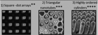
|
Photonic devices |
| Ordered nanoporous structureb |
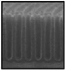
|
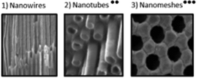
|
Structural coloration Fabry Pérot adsorption |
| Branched structurec |
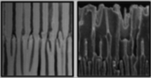
|
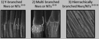
|
Drug delivery biosensors |
| Modulated in diameter nanoporesd |
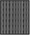
|
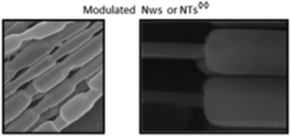
|
Structural coloration: DBR, photonic crystals, optical microcavities, graded index filters and biosensors |
| Nanoporous structuree |
|
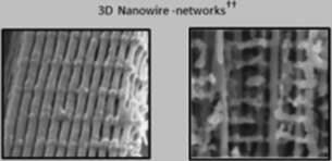
|
Structural coloration: Distributed Bragg, reflector, photonic crystals and biosensors |
Finally, the most recent and relevant examples of the state-of-the-art developments and applications based on AAO membranes have been shown, from their use for structural coloration to distributed Bragg reflectors, drug delivery, and sensing applications (see Table 2). The engineering of these nanostructures enables the development of novel approaches to different problems encountered in a great variety of fields. Some of these future applications appear nowadays as challenges that are being tackled, such as the fabrication of nanowires or 3D nanostructured metamaterials with tailored properties, or the design of novel AAO nanostructures, with direct applications in fields such as biotechnology, optical detection, energy storage, conversion and generation, and filtering. For instance, 3D-AAO templates provide a way of obtaining an assembly of mechanically robust nanowires, making it possible to obtain scaffolds of interconnected nanowires. Also, the 3D-AAO structure itself provides a much higher surface to volume ratio than other structures, which can be beneficial for techniques that use activated surfaces, such as bio-sensing (virus detection, DNA, etc.). Most importantly, these AAO platforms will also be the answer to problems not envisaged yet in fields where they have not been traditionally used, where their outstanding properties such as thermal, chemical, and mechanical stability, control over morphology, and large area coverage can be determinant to find novel solutions.
The number of original works based on AAO membranes discussed in this review, either using their nanostructuring possibilities to nanostructure different materials in a scalable way or to directly exploit their properties, justify the importance that the understanding of their growth mechanisms has to be further developed to gain finer control over their structures. Thus, AAO membranes are a powerful and promising platform to explore novel metamaterials through nanostructuration and creative applications in a wide range of fields.
Conflicts of interest
There are no conflicts to declare.Acknowledgements
The authors would like to acknowledge the project MAT2017-86450-c4-3-r, PIE-201950E057, and CAM18-PRE-IMN-001 fellowship of ARC. We also acknowledge the support of the publication fee by the CSIC Open Access Publication Support Initiative through its Unit of Information Resources for Research (URICI).Notes and references
- H. Masuda, H. Tanaka and N. Baba, Chem. Lett., 1990, 19, 621–622 CrossRef.
- K. Schwirn, W. Lee, R. Hillebrand, M. Steinhart, K. Nielsch and U. Gösele, ACS Nano, 2008, 2, 302–310 CrossRef CAS.
- C. V. Manzano, J. Martín and M. S. Martín-González, Microporous Mesoporous Mater., 2014, 184, 177–183 CrossRef CAS.
- W. Lee, R. Ji, U. Gösele and K. Nielsch, Nat. Mater., 2006, 5, 741 CrossRef CAS.
- V. Vega, J. García, J. M. Montero-Moreno, B. Hernando, J. Bachmann, V. M. Prida and K. Nielsch, ACS Appl. Mater. Interfaces, 2015, 7, 28682–28692 CrossRef CAS.
- Y. Li, M. Zheng, L. Ma and W. Shen, Nanotechnology, 2006, 17, 5101–5105 CrossRef CAS.
- S. Akiya, T. Kikuchi, S. Natsui, N. Sakaguchi and R. O. Suzuki, Electrochim. Acta, 2016, 190, 471–479 CrossRef CAS.
- A. Takenaga, T. Kikuchi, S. Natsui and R. O. Suzuki, ECS Solid State Lett., 2015, 4, P55–P58 CrossRef CAS.
- S. Ono, M. Saito and H. Asoh, Electrochim. Acta, 2005, 51, 827–833 CrossRef CAS.
- T. Kikuchi, O. Nishinaga, S. Natsui and R. O. Suzuki, Electrochim. Acta, 2015, 156, 235–243 CrossRef CAS.
- S. Akiya, T. Kikuchi, S. Natsui and R. O. Suzuki, Appl. Surf. Sci., 2017, 403, 652–661 CrossRef CAS.
- J. Martín, C. V. Manzano, O. Caballero-Calero and M. Martín-González, ACS Appl. Mater. Interfaces, 2013, 5, 72–79 CrossRef.
- J. Martín, C. V. Manzano and M. Martín-González, Microporous Mesoporous Mater., 2012, 151, 311–316 CrossRef.
- L. M. Ferro, S. G. Lemos, M. Ferreira and F. Trivinho-Strixino, Sens. Actuators, B, 2017, 248, 718–723 CrossRef CAS.
- T. Kumeria, A. Santos, M. M. Rahman, J. Ferré-Borrull, L. F. Marsal and D. Losic, ACS Photonics, 2014, 1, 1298–1306 CrossRef CAS.
- J. Lee, K. Bae, G. Kang, M. Choi, S. Baek, D.-S. Yoo, C.-W. Lee and K. Kim, RSC Adv., 2015, 5, 71770–71777 RSC.
- Y. Chen, A. Santos, Y. Wang, T. Kumeria, D. Ho, J. Li, C. Wang and D. Losic, Sci. Rep., 2015, 5, 12893 CrossRef CAS.
- G. Sriram, P. Patil, M. P. Bhat, R. M. Hegde, K. V. Ajeya, I. Udachyan, M. Bhavya, M. G. Gatti, U. Uthappa and G. M. Neelgund, J. Nanomater., 2016, 2016, 1753574 CrossRef.
- M. A. Tabrizi, J. Ferré-Borrull and L. F. Marsal, Biosens. Bioelectron., 2020, 149, 111828 CrossRef.
- T. Lednicky and A. Bonyár, ACS Appl. Mater. Interfaces, 2020, 4, 4804–4814 CrossRef.
- M. Porta-i-Batalla, E. Xifré-Pérez, C. Eckstein, J. Ferré-Borrull and L. F. Marsal, Nanomaterials, 2017, 7, 227 CrossRef.
- S. Simovic, D. Losic and K. Vasilev, Chem. Commun., 2010, 46, 1317–1319 RSC.
- G. Jeon, S. Y. Yang, J. Byun and J. K. Kim, Nano Lett., 2011, 11, 1284–1288 CrossRef CAS.
- T. Kumeria, J. Yu, M. Alsawat, M. D. Kurkuri, A. Santos, A. D. Abell and D. Losic, Modulating molecular transport across peptide-modified nanoporous alumina membranes with light, in SPIE BioPhotonics Australasia, International Society for Optics and Photonics, 2016, vol. 10013, p. 100131W Search PubMed.
- M. Porta-i-Batalla, C. Eckstein, E. Xifré-Pérez, P. Formentín, J. Ferré-Borrull and L. F. Marsal, Nanoscale Res. Lett., 2016, 11, 372 CrossRef.
- A. M. Mebed, A. M. Abd-Elnaiem and N. M. Al-Hosiny, Appl. Phys. A, 2016, 122, 565 CrossRef.
- F. Domínguez-Adame, M. Martín-González, D. Sánchez and A. Cantarero, Phys. E, 2019, 113, 213–225 CrossRef.
- C. V. Manzano and M. Martin-Gonzalez, Front. Chem., 2019, 7, 516 CrossRef CAS.
- G. Zhang, H. Fang, H. Yang, L. A. Jauregui, Y. P. Chen and Y. Wu, Nano Lett., 2012, 12, 3627–3633 CrossRef CAS.
- H.-P. Wang, K.-T. Tsai, K.-Y. Lai, T.-C. Wei, Y.-L. Wang and J.-H. He, Opt. Express, 2012, 20, A94–A103 CrossRef CAS.
- Y. Shirai, S. Takami, S. Lasmono, H. Iwai, T. Chikyow and Y. Wakayama, J. Polym. Sci., Part B: Polym. Phys., 2011, 49, 1762–1768 CrossRef CAS.
- D. O'Carroll, D. Iacopino, A. O'Riordan, P. Lovera, É. O'Connor, G. A. O'Brien and G. Redmond, Adv. Mater., 2008, 20, 42–48 CrossRef.
- C. Manzano, G. Bürki, L. Pethö, J. Michler and L. Philippe, J. Mater. Chem. C, 2017, 5, 1706–1713 RSC.
- C. d. Frantz, A. Lauria, C. V. Manzano, C. Guerra-Nuñez, M. Niederberger, C. d. Storrer, J. Michler and L. Philippe, Langmuir, 2017, 33, 12404–12418 CrossRef CAS.
- E. Bertero, C. V. Manzano, G. Bürki and L. Philippe, Mater. Des., 2020, 108559 CrossRef CAS.
- J. García, V. Vega, L. Iglesias, V. M. Prida, B. Hernando, E. D. Barriga-Castro, R. Mendoza-Reséndez, C. Luna, D. Görlitz and K. Nielsch, Phys. Status Solidi A, 2014, 211, 1041–1047 CrossRef.
- M. S. Salem, F. Tejo, R. Zierold, P. Sergelius, J. M. M. Moreno, D. Goerlitz, K. Nielsch and J. Escrig, Nanotechnology, 2018, 29, 065602 CrossRef.
- Y. P. Ivanov, A. Chuvilin, S. Lopatin and J. Kosel, ACS Nano, 2016, 10, 5326–5332 CrossRef CAS.
- M. S. Salem, P. Sergelius, R. M. Corona, J. Escrig, D. Görlitz and K. Nielsch, Nanoscale, 2013, 5, 3941–3947 RSC.
- C. Zhao, Q. Li, W. Wan, J. Li, J. Li, H. Zhou and D. Xu, J. Mater. Chem., 2012, 22, 12193–12197 RSC.
- M. P. Proenca, C. T. Sousa, J. Ventura and J. P. Araújo, in Magnetic Nano- and Microwires, ed. M. Vázquez, Woodhead Publishing, 2nd edn, 2020, pp. 135–184, DOI:10.1016/B978-0-08-102832-2.00006-2.
- K. Žužek Rožman, D. Pečko, S. Šturm, U. Maver, P. Nadrah, M. Bele and S. Kobe, Mater. Chem. Phys., 2012, 133, 218–224 CrossRef.
- B. I. Seo, U. A. Shaislamov, M. H. Ha, S. W. Kim, H. K. Kim and B. Yang, Physica E, 2007, 37, 241–244 CrossRef CAS.
- M. Norek, M. Putkonen, W. Zaleszczyk, B. Budner and Z. Bojar, Mater. Charact., 2018, 136, 52–59 CrossRef CAS.
- J. S. Lee, G. H. Gu, H. Kim, K. S. Jeong, J. Bae and J. S. Suh, Chem. Mater., 2001, 13, 2387–2391 CrossRef CAS.
- M. Alsawat, T. Altalhi, A. Santos and D. Losic, J. Phys. Chem. C, 2017, 121, 13634–13644 CrossRef CAS.
- J.-W. Back, S. Lee, C.-R. Hwang, C.-S. Chi and J.-Y. Kim, Macromol. Res., 2011, 19, 33–37 CrossRef CAS.
- J. Byun, Y. Kim, G. Jeon and J. K. Kim, Macromolecules, 2011, 44, 8558–8562 CrossRef CAS.
- R. M. Córdova-Castro, A. V. Krasavin, M. E. Nasir, A. V. Zayats and W. Dickson, Nanotechnology, 2018, 30, 055301 CrossRef.
- G. Meng, F. Han, X. Zhao, B. Chen, D. Yang, J. Liu, Q. Xu, M. Kong, X. Zhu, Y. J. Jung, Y. Yang, Z. Chu, M. Ye, S. Kar, R. Vajtai and P. M. Ajayan, Angew. Chem., Int. Ed., 2009, 48, 7166–7170 CrossRef CAS.
- L. Sacco, I. Florea, M. Châtelet and C.-S. Cojocaru, J. Phys.: Mater., 2018, 1, 015004 CAS.
- Y. Tian, G. Meng, S. K. Biswas, P. M. Ajayan, S. Sun and L. Zhang, Appl. Phys. Lett., 2004, 85, 967–969 CrossRef CAS.
- B. Chen, Q. Xu, X. Zhao, X. Zhu, M. Kong and G. Meng, Adv. Funct. Mater., 2010, 20, 3791–3796 CrossRef CAS.
- X. Li, G. Meng, Q. Xu, M. Kong, X. Zhu, Z. Chu and A.-P. Li, Nano Lett., 2011, 11, 1704–1709 CrossRef CAS.
- S. Mahima, R. Kannan, I. Komath, M. Aslam and V. K. Pillai, Chem. Mater., 2008, 20, 601–603 CrossRef CAS.
- H. Jo, N. Haberkorn, J.-A. Pan, M. Vakili, K. Nielsch and P. Theato, Langmuir, 2016, 32, 6437–6444 CrossRef CAS.
- S. P. Zankowski and P. M. Vereecken, ACS Appl. Mater. Interfaces, 2018, 10, 44634–44644 CrossRef CAS.
- N. Kim, E. Sahadeo, C. Liu, O. Rose, G. Rubloff and S. B. Lee, Phys. Chem. Chem. Phys., 2018, 20, 29708–29716 RSC.
- A. Ruiz-Clavijo, S. Ruiz-Gomez, O. Caballero-Calero, L. Perez and M. Martin-Gonzalez, Phys. Status Solidi RRL, 2019, 13, 1900263 CrossRef CAS.
- A. Ruiz-Clavijo, O. Caballero-Calero and M. Martín-González, Nanomaterials, 2018, 8, 345 CrossRef.
- P. M. Resende, R. Sanz, O. Caballero-Calero and M. Martín-González, Adv. Opt. Mater., 2018, 6, 1800408 CrossRef.
- A. García-Barberá, M. Culebras, S. Roig-Sánchez, C. M. Gómez and A. Cantarero, Synth. Met., 2016, 220, 208–212 CrossRef.
- D. Navas, F. Ilievski and C. A. Ross, J. Appl. Phys., 2009, 105, 113921 CrossRef.
- M. Vázquez, K. R. Pirota, D. Navas, A. Asenjo, M. Hernández-Vélez, P. Prieto and J. M. Sanz, J. Magn. Magn. Mater., 2008, 320, 1978–1983 CrossRef.
- Y. Xiang, Q.-l. Xia, J.-h. Luo, Y.-p. Liu, Y.-d. Peng, D.-w. Wang, Y.-z. Nie and G.-h. Guo, Solid State Commun., 2018, 281, 1–5 CrossRef CAS.
- J. A. Perez-Taborda, M. Muñoz Rojo, J. Maiz, N. Neophytou and M. Martin-Gonzalez, Sci. Rep., 2016, 6, 32778 CrossRef CAS.
- J. Tang, H.-T. Wang, D. H. Lee, M. Fardy, Z. Huo, T. P. Russell and P. Yang, Nano Lett., 2010, 10, 4279–4283 CrossRef CAS.
- Z. Zeng, X. Huang, Z. Yin, H. Li, Y. Chen, H. Li, Q. Zhang, J. Ma, F. Boey and H. Zhang, Adv. Mater., 2012, 24, 4138–4142 CrossRef CAS.
- L. Zhang, L. Jin, B. Liu and J. He, Front. Chem., 2019, 7, 22 CrossRef CAS.
- V. Malgras, Q. Ji, Y. Kamachi, T. Mori, F.-K. Shieh, K. C.-W. Wu, K. Ariga and Y. Yamauchi, Bull. Chem. Soc. Jpn., 2015, 88, 1171–1200 CrossRef CAS.
- G. Williams, M. Hunt, B. Boehm, A. May, M. Taverne, D. Ho, S. Giblin, D. Read, J. Rarity and R. Allenspach, Nano Res., 2018, 11, 845–854 CrossRef.
- M. F. Wagner, F. Völklein, H. Reith, C. Trautmann and M. E. Toimil-Molares, Phys. Status Solidi A, 2016, 213, 610–619 CrossRef CAS.
- C. Li, Q. Li, Y. V. Kaneti, D. Hou, Y. Yamauchi and Y. Mai, Chem. Soc. Rev., 2020, 49, 4681–4736 RSC.
- Q. Wang and D. Astruc, Chem. Rev., 2019, 120, 1438–1511 CrossRef.
- C. Healy, K. M. Patil, B. H. Wilson, L. Hermanspahn, N. C. Harvey-Reid, B. I. Howard, C. Kleinjan, J. Kolien, F. Payet and S. G. Telfer, Coord. Chem. Rev., 2020, 419, 213388 CrossRef CAS.
- B. Singh, J. Na, M. Konarova, T. Wakihara, Y. Yamauchi, C. Salomon and M. B. Gawande, Bull. Chem. Soc. Jpn., 2020, 93, 1459–1496 CrossRef CAS.
- L. Vera-Londono, A. Ruiz-Clavijo, O. Caballero-Calero and M. Martín-González, Nanoscale Adv., 2020, 2, 4591–4603 RSC.
- K. Nishio, Electrochem. Commun., 2017, 82, 30–33 CrossRef CAS.
- Y. Yang, H. Fei, G. Ruan and J. M. Tour, Adv. Mater., 2015, 27, 3175–3180 CrossRef CAS.
- B. Hu, W. Zhang, C. Yu, Z. Zheng, Y. Chen, J. Wang, J. Liu, K. Ma and W. Ren, Ind. Eng. Chem. Res., 2019, 58, 7131–7138 CrossRef CAS.
- B. Pandey, P. S. Thapa, D. A. Higgins and T. Ito, Langmuir, 2012, 28, 13705–13711 CrossRef CAS.
- A. Zaffora, F. Di Franco, F. Di Quarto, R. Macaluso, M. Mosca, H. Habazaki and M. Santamaria, ECS J. Solid State Sci. Technol., 2017, 6, N25 CrossRef CAS.
- M. Martin-Gonzalez, R. Martinez-Moro, M. H. Aguirre, E. Flores and O. Caballero-Calero, Electrochim. Acta, 2020, 330, 135241 CrossRef CAS.
- J. S. Kang, J. Kim, M. J. Lee, Y. J. Son, D. Y. Chung, S. Park, J. Jeong, J. M. Yoo, H. Shin and H. Choe, Adv. Sci., 2018, 5, 1700601 CrossRef.
- M. Altomare, G. Cha and P. Schmuki, Electrochim. Acta, 2020, 136158 CrossRef CAS.
- L. Zaraska, K. Gawlak, M. Gurgul, M. Dziurka, M. Nowak, D. Gilek and G. D. Sulka, Appl. Surf. Sci., 2018, 439, 672–680 CrossRef CAS.
- R. Sanz, M. A. Buccheri, M. Zimbone, V. Scuderi, G. Amiard, G. Impellizzeri, L. Romano and V. Privitera, Appl. Surf. Sci., 2017, 399, 451–462 CrossRef CAS.
- J. Kapusta-Kołodziej, A. Chudecka and G. D. Sulka, J. Electroanal. Chem., 2018, 823, 221–233 CrossRef.
- T. Kikuchi, J. Kawashima, S. Natsui and R. O. Suzuki, Appl. Surf. Sci., 2017, 422, 130–137 CrossRef CAS.
- H. Lee, V. S. Kumbhar, J. Lee, Y. Choi and K. Lee, Electrochim. Acta, 2020, 334, 135618 CrossRef CAS.
- K. Mika, R. P. Socha, P. Nyga, E. Wiercigroch, K. Małek, M. Jarosz, T. Uchacz, G. D. Sulka and L. Zaraska, Electrochim. Acta, 2019, 305, 349–359 CrossRef CAS.
- S. N. Patel, V. Jayaram and D. Banerjee, Surf. Coat. Technol., 2017, 323, 2–9 CrossRef CAS.
- G. E. Thompson and G. C. Wood, in Treatise on Materials Science and Technology, ed. J. C. Scully, Elsevier, 1983, vol. 23, pp. 205–329 Search PubMed.
- S. Chu, K. Wada, S. Inoue, M. Isogai, Y. Katsuta and A. Yasumori, J. Electrochem. Soc., 2006, 153, B384–B391 CrossRef CAS.
- J. O'Sullivan and G. Wood, Proc. R. Soc. London, Ser. A, 1970, 317, 511–543 Search PubMed.
- S. Ono, M. Saito, M. Ishiguro and H. Asoh, J. Electrochem. Soc., 2004, 151, B473 CrossRef CAS.
- K. Nielsch, J. Choi, K. Schwirn, R. B. Wehrspohn and U. Gösele, Nano Lett., 2002, 2, 677–680 CrossRef CAS.
- F. Li, L. Zhang and R. M. Metzger, Chem. Mater., 1998, 10(9), 2470–2480 CrossRef CAS.
- G. Sulka and K. G. Parkoła, Electrochim. Acta, 2007, 52, 1880–1888 CrossRef CAS.
- S.-K. Hwang, S.-H. Jeong, H.-Y. Hwang, O.-J. Lee and K.-H. Lee, Korean J. Chem. Eng., 2002, 19, 467–473 CrossRef CAS.
- V. Parkhutik and V. Shershulsky, J. Phys. D: Appl. Phys., 1992, 25, 1258 CrossRef CAS.
- M. Pashchanka and J. J. Schneider, J. Phys. Chem. C, 2016, 120, 14590–14596 CrossRef CAS.
- A. L. Friedman, D. Brittain and L. Menon, J. Chem. Phys., 2007, 127, 154717 CrossRef.
- G. D. Sulka, Nanostruct. Mater. Electrochem., 2008, 1, 1–116 Search PubMed.
- D. Losic and A. Santos, Nanoporous Alumina: Fabrication, Structure, Properties and Applications, Springer Series in Materials Science, Springer International Publishing Switzerland, 2015, vol. 219, ISBN 978-3-319-20333-1 Search PubMed.
- W. Lee and S.-J. Park, Chem. Rev., 2014, 114, 7487–7556 CrossRef CAS.
- O. Nishinaga, T. Kikuchi, S. Natsui and R. O. Suzuki, Sci. Rep., 2013, 3, 2748 CrossRef.
- T. Kikuchi, O. Nishinaga, S. Natsui and R. O. Suzuki, Electrochim. Acta, 2014, 137, 728–735 CrossRef CAS.
- S. Akiya, T. Kikuchi, S. Natsui and R. O. Suzuki, J. Electrochem. Soc., 2015, 162, E244–E250 CrossRef CAS.
- W. J. Stępniowski, M. Moneta, M. Norek, M. Michalska-Domańska, A. Scarpellini and M. Salerno, Electrochim. Acta, 2016, 211, 453–460 CrossRef.
- S. Stojadinovic, R. Vasilic, I. Belca, M. Tadic, B. Kasalica and L. Zekovic, Appl. Surf. Sci., 2008, 255, 2845–2850 CrossRef CAS.
- R. Kondo, D. Nakajima, T. Kikuchi, S. Natsui and R. O. Suzuki, J. Alloys Compd., 2017, 725, 379–387 CrossRef CAS.
- W. Lee, K. Nielsch and U. Gösele, Nanotechnology, 2007, 18, 475713 CrossRef.
- J. Bellemare, F. Sirois and D. Ménard, J. Electrochem. Soc., 2014, 161, E75 CrossRef CAS.
- H. Masuda and K. Fukuda, Science, 1995, 268, 1466–1468 CrossRef CAS.
- H. Masuda, K. Yada and A. Osaka, Jpn. J. Appl. Phys., 1998, 37, L1340–L1342 CrossRef.
- H. Masuda, J. Electrochem. Soc., 1997, 144, L127 CrossRef CAS.
- X. Chen, D. Yu, L. Cao, X. Zhu, Y. Song, H. Huang, L. Lu and X. Chen, Mater. Res. Bull., 2014, 57, 116–120 CrossRef CAS.
- S.-Z. Chu, K. Wada, S. Inoue, M. Isogai and A. Yasumori, Adv. Mater., 2005, 17, 2115–2119 CrossRef CAS.
- O. Jessensky, F. Muller and U. Gosele, Appl. Phys. Lett., 1998, 72, 1173–1175 CrossRef CAS.
- E. O. Gordeeva, I. V. Roslyakov and K. S. Napolskii, Electrochim. Acta, 2019, 307, 13–19 CrossRef CAS.
- S. Shingubara, K. Morimoto, H. Sakaue and T. Takahagi, Electrochem. Solid-State Lett., 2004, 7, E15 CrossRef CAS.
- M. Almasi Kashi, A. Ramazani, Y. Mayamai and M. Noormohammadi, Jpn. J. Appl. Phys., 2010, 49, 015202 CrossRef.
- Y.-f. Xu, H. Liu, X.-j. Li, W.-m. Kang, B.-w. Cheng and X.-j. Li, Mater. Lett., 2015, 151, 79–81 CrossRef CAS.
- M. Almasi Kashi and A. Ramazani, Int. J. Nanosci. Nanotechnol., 2010, 6, 78–87 Search PubMed.
- H. A. Rayat Azimi, M. Zarei, A. Rafati and M. Noormohammadi, J. Porous Mater., 2016, 23, 357–363 CrossRef CAS.
- R. Kanakala, P. Singaraju, R. Venkat and B. Das, J. Electrochem. Soc., 2005, 152, J1–J5 CrossRef CAS.
- E. Verwey, Physica, 1935, 2, 1059–1063 CrossRef CAS.
- N. Cabrera and N. F. Mott, Rep. Prog. Phys., 1949, 12, 163–184 CrossRef CAS.
- J. Dewald, J. Electrochem. Soc., 1955, 102, 1 CrossRef CAS.
- L. Zhang, D. D. Macdonald, E. Sikora and J. Sikora, J. Electrochem. Soc., 1998, 145, 898 CrossRef CAS.
- M. Lohrengel, Mater. Sci. Eng., R, 1993, 11, 243–294 CrossRef.
- D. LeClere, A. Velota, P. Skeldon, G. Thompson, S. Berger, J. Kunze, P. Schmuki, H. Habazaki and S. Nagata, J. Electrochem. Soc., 2008, 155, C487 CrossRef CAS.
- K. Shimizu, K. Kobayashi, G. Thompson and G. Wood, Philos. Mag. A, 1992, 66, 643–652 CrossRef CAS.
- F. Keller, M. Hunter and D. Robinson, J. Electrochem. Soc., 1953, 100, 411 CrossRef CAS.
- T. Hoar and J. Yahalom, J. Electrochem. Soc., 1963, 110, 614–621 CrossRef CAS.
- G. Wood and J. O'Sullivan, Electrochim. Acta, 1970, 15, 1865–1876 CrossRef CAS.
- G. Thompson, Thin Solid Films, 1997, 297, 192–201 CrossRef CAS.
- S. Garcia-Vergara, P. Skeldon, G. Thompson and H. Habazaki, Electrochim. Acta, 2006, 52, 681–687 CrossRef CAS.
- J. E. Houser and K. R. Hebert, Nat. Mater., 2009, 8, 415–420 CrossRef CAS.
- J. E. Houser and K. R. Hebert, Phys. Status Solidi A, 2008, 205, 2396–2399 CrossRef CAS.
- K. R. Hebert and J. E. Houser, J. Electrochem. Soc., 2009, 156, C275–C281 CrossRef CAS.
- X. Zhu, L. Liu, Y. Song, H. Jia, H. Yu, X. Xiao and X. Yang, Monatsh. Chem. – Chem. Monthly, 2008, 139, 999–1003 CrossRef CAS.
- M. Nagayama and K. Tamura, Electrochim. Acta, 1967, 12, 1097–1107 CrossRef CAS.
- R. B. Mason, J. Electrochem. Soc., 1955, 102, 671 CrossRef CAS.
- J. Oh, Porous Anodic Aluminum Oxide Scaffolds, Formation Mechanisms and Applications, Massachusetts Institute of Technology, 2010.
- M. Hunter and P. Fowle, J. Electrochem. Soc., 1954, 101, 514 CrossRef CAS.
- S. K. Thamida and H.-C. Chang, Chaos, 2002, 12, 240–251 CrossRef CAS.
- G. Singh, A. Golovin and I. Aranson, Phys. Rev. B: Condens. Matter Mater. Phys., 2006, 73, 205422 CrossRef.
- J. E. Houser and K. R. Hebert, J. Electrochem. Soc., 2006, 153, B566–B573 CrossRef CAS.
- Z. Su, G. Hähner and W. Zhou, J. Mater. Chem., 2008, 18, 5787–5795 RSC.
- J. Siejka and C. Ortega, J. Electrochem. Soc., 1977, 124, 883–891 CrossRef CAS.
- A. Baron-Wiecheć, J. Ganem, S. Garcia-Vergara, P. Skeldon, G. Thompson and I. Vickridge, J. Electrochem. Soc., 2010, 157, C399–C407 CrossRef.
- H. Takahashi and M. Nagayama, Corros. Sci., 1978, 18, 911–925 CrossRef CAS.
- Z. Wu, C. Richter and L. Menon, J. Electrochem. Soc., 2007, 154, E8–E12 CrossRef CAS.
- P. Skeldon, G. Thompson, S. Garcia-Vergara, L. Iglesias-Rubianes and C. Blanco-Pinzon, Electrochem. Solid-State Lett., 2006, 9, B47–B51 CrossRef CAS.
- N. Sato, Electrochim. Acta, 1971, 16, 1683–1692 CrossRef CAS.
- A. Li, F. Müller, A. Birner, K. Nielsch and U. Gösele, J. Appl. Phys., 1998, 84, 6023–6026 CrossRef CAS.
- I. Vrublevsky, V. Parkoun, V. Sokol, J. Schreckenbach and G. Marx, Appl. Surf. Sci., 2004, 222, 215–225 CrossRef CAS.
- I. Vrublevsky, V. Parkoun, J. Schreckenbach and G. Marx, Appl. Surf. Sci., 2003, 220, 51–59 CrossRef CAS.
- S. Ono and N. Masuko, Corros. Sci., 1992, 33, 503–507 CrossRef CAS.
- H. Takahashi, K. Fujimoto, H. Konno and M. Nagayama, J. Electrochem. Soc., 1984, 131, 1856 CrossRef CAS.
- I. Mínguez-Bacho, S. Rodríguez-López, A. Climent, D. Fichou, M. Vázquez and M. Hernández-Vélez, J. Phys. Chem. C, 2015, 119, 27392–27400 CrossRef.
- P. Mishra and K. R. Hebert, Electrochim. Acta, 2016, 222, 1186–1190 CrossRef CAS.
- K. R. Hebert and P. Mishra, J. Electrochem. Soc., 2018, 165, E737–E743 CrossRef CAS.
- K. R. Hebert and P. Mishra, J. Electrochem. Soc., 2018, 165, E744–E750 CrossRef CAS.
- P. Mishra and K. R. Hebert, Electrochim. Acta, 2020, 135879 CrossRef CAS.
- S. Garcia-Vergara, H. Habazaki, P. Skeldon and G. Thompson, Nanotechnology, 2007, 18, 415605 CrossRef.
- S. Garcia-Vergara, P. Skeldon, G. Thompson and H. Habazaki, Corros. Sci., 2007, 49, 3772–3782 CrossRef CAS.
- F.-y. Zhou, A. M. Al-Zenati, A. Baron-Wiecheć, M. Curioni, S. Garcia-Vergara, H. Habazaki, P. Skeldon and G. Thompson, J. Electrochem. Soc., 2011, 158, C202 CrossRef CAS.
- X. Zhu, D. Li, Y. Song and Y. Xiao, Mater. Lett., 2005, 59, 3160–3163 CrossRef CAS.
- D. Li, C. Jiang, J. Jiang and J. G. Lu, Chem. Mater., 2009, 21, 253–258 CrossRef CAS.
- D. Li, L. Zhao, C. Jiang and J. G. Lu, Nano Lett., 2010, 10, 2766–2771 CrossRef CAS.
- X.-F. Zhu, Y. Song, L. Liu, C.-Y. Wang, J. Zheng, H.-B. Jia and X.-L. Wang, Nanotechnology, 2009, 20, 475303 CrossRef.
- H. Fan, T. Lin, W. Zhang, J. Ma, S. Lu and X. Zhu, Mater. Res. Bull., 2017, 90, 119–124 CrossRef CAS.
- S. Heinschke and J. J. Schneider, J. Phys. Chem. C, 2020, 124, 11913–11921 CrossRef CAS.
- M. Pashchanka, Phys. Chem. Chem. Phys., 2020, 22(28), 15867–15875 RSC.
- M. Pashchanka and J. J. Schneider, J. Mater. Chem., 2011, 21, 18761–18767 RSC.
- H. Masuda and M. Satoh, Jpn. J. Appl. Phys., 1996, 35, L126 CrossRef CAS.
- B. Chen, K. Lu and Z. Tian, Langmuir, 2011, 27, 800–808 CrossRef CAS.
- K. Lu, Electrochim. Acta, 2012, 63, 256–262 CrossRef CAS.
- B. Chen and K. Lu, Langmuir, 2011, 27, 4117–4125 CrossRef CAS.
- Z. Tian, K. Lu and B. Chen, J. Appl. Phys., 2010, 108, 094306 CrossRef.
- K. Lu and J. Zhao, J. Nanosci. Nanotechnol., 2010, 10, 6760–6768 CrossRef CAS.
- S. Shingubara, Y. Murakami, K. Morimoto and T. Takahagi, Surf. Sci., 2003, 532, 317–323 CrossRef.
- M. Jaafar, D. Navas, M. Hernández-Vélez, J. Baldonedo, M. Vázquez and A. Asenjo, Surf. Sci., 2009, 603, 3155–3159 CrossRef CAS.
- Z. Sun and H. K. Kim, Appl. Phys. Lett., 2002, 81, 3458–3460 CrossRef CAS.
- B. Kim, S. Park, T. J. McCarthy and T. P. Russell, Small, 2007, 3, 1869–1872 CrossRef CAS.
- A. Yin, M. Tzolov, D. Cardimona, L. Guo and J. Xu, IET Circuits, Devices Syst., 2007, 1, 205–209 CrossRef.
- V. Stasi, G. Cattaneo, S. Franz, M. Bestetti, M. Ubaldi, D. Piccinin and S. M. Pietralunga, Photonics and Nanostructures-Fundamentals and Applications, 2007, 5, 136–139 Search PubMed.
- T. S. Kustandi, W. W. Loh, H. Gao and H. Y. Low, ACS Nano, 2010, 4, 2561–2568 CrossRef CAS.
- J. T. Smith, Q. Hang, A. D. Franklin, D. B. Janes and T. D. Sands, Appl. Phys. Lett., 2008, 93, 043108 CrossRef.
- A. Maria Chong, L. K. Tan, J. Deng and H. Gao, Adv. Funct. Mater., 2007, 17, 1629–1635 CrossRef.
- H. Masuda, H. Yamada, M. Satoh, H. Asoh, M. Nakao and T. Tamamura, Appl. Phys. Lett., 1997, 71, 2770–2772 CrossRef CAS.
- H. Masuda, M. Yotsuya, M. Asano, K. Nishio, M. Nakao, A. Yokoo and T. Tamamura, Appl. Phys. Lett., 2001, 78, 826–828 CrossRef CAS.
- W. Lee, R. Ji, C. A. Ross, U. Gösele and K. Nielsch, Small, 2006, 2, 978–982 CrossRef CAS.
- D. Navas, O. Sanchez, A. Asenjo, M. Jaafar, J. Baldonedo, M. Vazquez and M. Hernandez-Velez, Nanotechnology, 2007, 18, 165302 CrossRef.
- X. Wang, S. Xu, M. Cong, H. Li, Y. Gu and W. Xu, Small, 2012, 8, 972–976 CrossRef CAS.
- W. Im, Y. Cho, G. Choi, F. Yu and D. Kim, Diamond Relat. Mater., 2004, 13, 1214–1217 CrossRef CAS.
- C. Sousa, A. Apolinário and D. Leitão, Adv. Nanotechnol., 2014, 12, 123 Search PubMed.
- A. Y. Y. Ho, H. Gao, Y. C. Lam and I. Rodriguez, Adv. Funct. Mater., 2008, 18, 2057–2063 CrossRef CAS.
- C. Shuoshuo, L. Zhiyuan, H. Xing, Y. Hui and L. Yi, J. Mater. Chem., 2010, 20, 1794–1798 RSC.
- R. Krishnan and C. V. Thompson, Adv. Mater., 2007, 19, 988–992 CrossRef CAS.
- C. Sousa, A. Apolinario, D. Leitao, A. Pereira, J. Ventura and J. Araujo, J. Mater. Chem., 2012, 22, 3110–3116 RSC.
- D. Guo, L. Fan, J. Sang, Y. Liu, S. Huang and X. Zou, Nanotechnology, 2007, 18, 405304 CrossRef.
- J. Zhang, C. S. Day and D. L. Carroll, Chem. Commun., 2009, 6937–6939 RSC.
- R. Zakeri, C. Watts, H. Wang and P. Kohli, Chem. Mater., 2007, 19, 1954–1963 CrossRef CAS.
- S. Jin, Y. Li, Z. Li, X. Hu, Z. Ling, X. He, Y. Shen and L. Jin, J. Electrochem. Soc., 2016, 163, H1053–H1059 CrossRef CAS.
- W. Cheng, M. Steinhart, U. Gösele and R. B. Wehrspohn, J. Mater. Chem., 2007, 17, 3493–3495 RSC.
- H. Hashimoto, S. Kojima, T. Sasaki and H. Asoh, J. Eur. Ceram. Soc., 2018, 38, 1836–1840 CrossRef CAS.
- G. D. Sulka, A. Brzózka and L. Liu, Electrochim. Acta, 2011, 56, 4972–4979 CrossRef CAS.
- M. Norek, W. J. Stępniowski and D. Siemiaszko, J. Electroanal. Chem., 2016, 762, 20–28 CrossRef CAS.
- P. Hoyer, K. Nishio and H. Masuda, Thin Solid Films, 1996, 286, 88–91 CrossRef CAS.
- L. Yi, L. Zhiyuan, C. Shuoshuo, H. Xing and H. Xinhua, Chem. Commun., 2010, 46, 309–311 RSC.
- L. Yi, L. Zhiyuan, H. Xing, L. Yisen and C. Yi, RSC Adv., 2012, 2, 5164–5171 RSC.
- G. D. Sulka and K. Hnida, Nanotechnology, 2012, 23, 075303 CrossRef.
- D. Losic, M. Lillo and D. Losic Jr., Small, 2009, 5, 1392–1397 CrossRef CAS.
- W. Lee and J.-C. Kim, Nanotechnology, 2010, 21, 485304 CrossRef.
- J. Liao, Surf. Eng. Appl. Electrochem., 2018, 54, 555–561 CrossRef.
- H. Bayat, C.-H. Lin, M.-H. Cheng, M. Steuber, J.-T. Chen and H. Schönherr, ACS Appl. Nano Mater., 2017, 1, 200–208 CrossRef.
- Y. Wang, A. Santos, A. Evdokiou and D. Losic, Electrochim. Acta, 2015, 154, 379–386 CrossRef CAS.
- J. Martín, M. Martín-González, J. F. Fernández and O. Caballero-Calero, Nat. Commun., 2014, 5, 5130 CrossRef.
- D. Losic and D. Losic Jr., Langmuir, 2009, 25, 5426–5431 CrossRef CAS.
- P. M. Resende, R. Sanz, A. Ruiz-Clavijo, O. Caballero-Calero and M. Martin-Gonzalez, Coatings, 2016, 6, 59 CrossRef.
- F. Matsumoto, M. Harada, N. Koura, K. Nishio and H. Masuda, Electrochem. Solid-State Lett., 2004, 7, E51 CrossRef CAS.
- J. Choi, J. Schilling, K. Nielsch, R. Hillebrand, M. Reiche, R. Wehrspohn and U. Gösele, MRS Online Proc. Libr. Arch., 2002, 722, 52 CrossRef.
- Z. Fan, H. Razavi, J.-w. Do, A. Moriwaki, O. Ergen, Y.-L. Chueh, P. W. Leu, J. C. Ho, T. Takahashi and L. A. Reichertz, Nat. Mater., 2009, 8, 648–653 CrossRef CAS.
- L. Wen, R. Xu, Y. Mi and Y. Lei, Nat. Nanotechnol., 2017, 12, 244–250 CrossRef CAS.
- Y. Xu, M. Zhou, L. Wen, C. Wang, H. Zhao, Y. Mi, L. Liang, Q. Fu, M. Wu and Y. Lei, Chem. Mater., 2015, 27, 4274–4280 CrossRef CAS.
- K. Yasui, K. Nishio and H. Masuda, Jpn. J. Appl. Phys., 2005, 44, L1181 CrossRef CAS.
- G. Fois, C. T. Bolger, J. D. Holmes and G. Cross, MRS Online Proc. Libr. Arch., 2010, 1258, 1258-Q05-01 CrossRef.
- J. Choi, R. B. Wehrspohn and U. Gösele, Electrochim. Acta, 2005, 50, 2591–2595 CrossRef CAS.
- H. Asoh, S. Ono, T. Hirose, I. Takatori and H. Masuda, Jpn. J. Appl. Phys., 2004, 43, 6342 CrossRef CAS.
- J. Choi, K. Nielsch, M. Reiche, R. Wehrspohn and U. Gösele, J. Vac. Sci. Technol., B: Microelectron. Nanometer Struct.–Process., Meas., Phenom., 2003, 21, 763–766 CrossRef CAS.
- S. Shingubara, S. Maruo, T. Yamashita, M. Nakao and T. Shimizu, Microelectron. Eng., 2010, 87, 1451–1454 CrossRef CAS.
- H. Masuda, Y. Matsui, M. Yotsuya, F. Matsumoto and K. Nishio, Chem. Lett., 2004, 33, 584–585 CrossRef CAS.
- S. Fournier-Bidoz, V. Kitaev, D. Routkevitch, I. Manners and G. A. Ozin, Adv. Mater., 2004, 16, 2193–2196 CrossRef CAS.
- Q. Xu, G. Meng and F. Han, Prog. Mater. Sci., 2018, 95, 243–285 CrossRef CAS.
- D. Routkevitch, A. Tager, J. Haruyama, D. Almawlawi, M. Moskovits and J. M. Xu, IEEE Trans. Electron Devices, 1996, 43, 1646–1658 CrossRef CAS.
- W. J. Stępniowski and M. Salerno, Manuf. Nanostruct., 2014, 12, 321–357 Search PubMed.
- H. Hashimoto, Y. Shigehara, S. Ono and H. Asoh, Microporous Mesoporous Mater., 2018, 265, 77–83 CrossRef CAS.
- L. Vera-Londono, A. Ruiz-Clavijo, O. Caballero-Calero and M. Martín-González, Nanoscale Adv., 2020, 2, 4591–4603 RSC.
- T. Huber, K. Owusu, S. Johnson, A. Nikolaeva, L. Konopko, R. Johnson and M. J. Graf, J. Appl. Phys., 2012, 111, 043709 CrossRef.
- M. Sistani, P. Staudinger, J. Greil, M. Holzbauer, H. Detz, E. Bertagnolli and A. Lugstein, Nano Lett., 2017, 17, 4556–4561 CrossRef CAS.
- J. Fang, S. Chen, W. G. Vandenberghe and M. V. Fischetti, IEEE Trans. Electron Devices, 2017, 64, 2758–2764 CAS.
- M. Muñoz Rojo, Y. Zhang, C. V. Manzano, R. Alvaro, J. Gooth, M. Salmeron and M. Martin-Gonzalez, Sci. Rep., 2016, 6, 19014 CrossRef.
- S. S. Parkin, M. Hayashi and L. Thomas, Science, 2008, 320, 190–194 CrossRef CAS.
- D. A. Allwood, G. Xiong, C. Faulkner, D. Atkinson, D. Petit and R. Cowburn, Science, 2005, 309, 1688–1692 CrossRef CAS.
- J. A. Fernandez-Roldan, R. P. del Real, C. Bran, M. Vazquez and O. Chubykalo-Fesenko, Nanoscale, 2018, 10, 5923–5927 RSC.
- C. Murapaka, P. Sethi, S. Goolaup and W. S. Lew, Sci. Rep., 2016, 6, 20130 CrossRef CAS.
- C. Bran, E. Berganza, J. A. Fernandez-Roldan, E. M. Palmero, J. Meier, E. Calle, M. Jaafar, M. Foerster, L. Aballe and A. Fraile Rodriguez, ACS Nano, 2018, 12, 5932–5939 CrossRef CAS.
- Y. P. Ivanov, M. Vázquez and O. Chubykalo-Fesenko, J. Phys. D: Appl. Phys., 2013, 46, 485001 CrossRef.
- S. Da Col, S. Jamet, N. Rougemaille, A. Locatelli, T. O. Mentes, B. S. Burgos, R. Afid, M. Darques, L. Cagnon and J.-C. Toussaint, Phys. Rev. B: Condens. Matter Mater. Phys., 2014, 89, 180405 CrossRef.
- R. Wieser, U. Nowak and K.-D. Usadel, Phys. Rev. B: Condens. Matter Mater. Phys., 2004, 69, 064401 CrossRef.
- H. Forster, T. Schrefl, W. Scholz, D. Suess, V. Tsiantos and J. Fidler, J. Magn. Magn. Mater., 2002, 249, 181–186 CrossRef CAS.
- M. Yan, A. Kákay, S. Gliga and R. Hertel, Phys. Rev. Lett., 2010, 104, 057201 CrossRef.
- S. S. Parkin, M. Hayashi and L. Thomas, Science, 2008, 320(5873), 190–194 CrossRef CAS.
- K. Pitzschel, J. Bachmann, S. Martens, J. M. Montero-Moreno, J. Kimling, G. Meier, J. Escrig, K. Nielsch and D. Görlitz, J. Appl. Phys., 2011, 109, 033907 CrossRef.
- Y. T. Chong, D. Görlitz, S. Martens, M. Y. E. Yau, S. Allende, J. Bachmann and K. Nielsch, Adv. Mater., 2010, 22, 2435–2439 CrossRef CAS.
- S. Samanifar, M. Alikhani, M. A. Kashi, A. Ramazani and A. Montazer, J. Magn. Magn. Mater., 2017, 430, 6–15 CrossRef CAS.
- A. Samardak, A. Ognev, A. Y. Samardak, E. Stebliy, E. Modin, L. Chebotkevich, S. Komogortsev, A. Stancu, E. Panahi-Danaei and A. Fardi-Ilkhichy, J. Alloys Compd., 2018, 732, 683–693 CrossRef CAS.
- S. Ruiz-Gómez, M. Foerster, L. Aballe, M. P. Proenca, I. Lucas, J. L. Prieto, A. Mascaraque, J. de la Figuera, A. Quesada and L. Pérez, Sci. Rep., 2018, 8, 1–6 CrossRef.
- M. Abbas, A. Ramazani, A. Montazer and M. A. Kashi, J. Appl. Phys., 2019, 125, 173902 CrossRef.
- N. Şarlı and M. Keskin, Solid State Commun., 2012, 152, 354–359 CrossRef.
- K. Liu, K. Nagodawithana, P. Searson and C. Chien, Phys. Rev. B: Condens. Matter Mater. Phys., 1995, 51, 7381 CrossRef CAS.
- H. Kamimura, M. Hayashida and T. Ohgai, Nanomaterials, 2020, 10, 5 CrossRef CAS.
- J. E. Perez and J. Kosel, in Magnetic Nano-and Microwires, Elsevier, 2020, pp. 697–713 Search PubMed.
- A. Prina-Mello, Z. Diao and J. M. D. Coey, J. Nanobiotechnol., 2006, 4, 9 CrossRef.
- Y. P. Ivanov, A. Alfadhel, M. Alnassar, J. E. Perez, M. Vazquez, A. Chuvilin and J. Kosel, Sci. Rep., 2016, 6, 24189 CrossRef CAS.
- A. I. Martínez-Banderas, A. Aires, S. Plaza-García, L. Colás, J. A. Moreno, T. Ravasi, J. S. Merzaban, P. Ramos-Cabrer, A. L. Cortajarena and J. Kosel, J. Nanobiotechnol., 2020, 18, 1–12 CrossRef.
- W.-S. Lin, H.-M. Lin, H.-H. Chen, Y.-K. Hwu and Y.-J. Chiou, J. Nanomater., 2013, 237439 Search PubMed.
- C. Rodríguez-Fernández, C. V. Manzano, A. H. Romero, J. Martín, M. Martín-González, M. Morais de Lima Jr. and A. Cantarero, Nanotechnology, 2016, 27, 075706 CrossRef.
- C. V. Manzano, M. N. Polyakov, J. Maiz, M. H. Aguirre, X. Maeder and M. Martín-González, Sci. Technol. Adv. Mater., 2019, 20, 1022–1030 CrossRef CAS.
- L. Hicks and M. S. Dresselhaus, Phys. Rev. B: Condens. Matter Mater. Phys., 1993, 47, 16631 CrossRef CAS.
- M. Dresselhaus, G. Dresselhaus, X. Sun, Z. Zhang, S. Cronin and T. Koga, Phys. Solid State, 1999, 41, 679–682 CrossRef CAS.
- M. M. Rojo, B. Abad, C. V. Manzano, P. Torres, X. Cartoixà, F. Alvarez and M. M. Gonzalez, Nanoscale, 2017, 9, 6741–6747 RSC.
- G. Gadea, A. Morata and A. Tarancon, in Semiconductors and Semimetals, Elsevier, 2018, vol. 98, pp. 321–407 Search PubMed.
- L. Shen, H. Du, J. Yang and Z. Ma, Appl. Surf. Sci., 2015, 325, 100–104 CrossRef CAS.
- R. Zhang, C. Zhao, B. Shao, J. Dong, J. Zhang and H. Yang, Broadband and quasi-omnidirectional antireflection Si subwavelength structure based on alumina nano-template directly formed on SiO2/Si, in Advances in Optoelectronics and Micro/nano-optics, IEEE, 2010, pp. 1–4 Search PubMed.
- H. Deniz, T. Khudiyev, F. Buyukserin and M. Bayindir, Appl. Phys. Lett., 2011, 99, 183107 CrossRef.
- L. Chen, J. Xie, K. R. Aatre and V. K. Varadan, J. Nanotechnol. Eng. Med., 2009, 1(1), 011009-1/8 Search PubMed.
- L. Chen, J. Xie, K. R. Aatre, J. Yancey, M. Srivatsan and V. K. Varadan, Nanosystems in Engineering and Medicine, International Society for Optics and Photonics, 2012, vol. 8548, p. 854867 Search PubMed.
- L. González-Souto, L. González-Rovira, F. J. Botana, J. J. Calvino, M. Á. Cauqui and J. C. Hernández-Garrido, Part. Part. Syst. Charact., 2019, 36, 1900168 CrossRef.
- P. Banerjee, I. Perez, L. Henn-Lecordier, S. B. Lee and G. W. Rubloff, Nat. Nanotechnol., 2009, 4, 292–296 CrossRef CAS.
- L. C. Haspert, S. B. Lee and G. W. Rubloff, ACS Nano, 2012, 6, 3528–3536 CrossRef CAS.
- Q. Lin, S.-F. Leung, L. Lu, X. Chen, Z. Chen, H. Tang, W. Su, D. Li and Z. Fan, ACS Nano, 2014, 8, 6484–6490 CrossRef CAS.
- A. Brzózka, D. Szeliga, E. Kurowska-Tabor and G. D. Sulka, Mater. Lett., 2016, 174, 66–70 CrossRef.
- M. M. Tavakoli, Q. Lin, S.-F. Leung, G. C. Lui, H. Lu, L. Li, B. Xiang and Z. Fan, Nanoscale, 2016, 8, 4276–4283 RSC.
- F. Béron, A. Kaidatzis, M. F. Velo, L. C. C. Arzuza, E. M. Palmero, R. P. del Real, D. Niarchos, K. R. Pirota and J. M. García-Martín, Nanoscale Res. Lett., 2016, 11, 86 CrossRef.
- C. Bran, P. Gawronski, I. Lucas, R. P. del Real, P. Strichovanec, A. Asenjo, M. Vazquez and O. Chubykalo-Fesenko, J. Phys. D: Appl. Phys., 2017, 50, 065003 CrossRef.
- T. N. A. Nguyen, J. Fedotova, J. Kasiuk, V. Bayev, O. Kupreeva, S. Lazarouk, D. H. Manh, D. L. Vu, S. Chung, J. Åkerman, V. Altynov and A. Maximenko, Appl. Surf. Sci., 2018, 427, 649–655 CrossRef CAS.
- M. T. Rahman, N. N. Shams, C. H. Lai, J. Fidler and D. Suess, Phys. Rev. B: Condens. Matter Mater. Phys., 2010, 81, 014418 CrossRef.
- A. Maximenko, M. Marszałek, J. Chojenka, J. Fedotova, B. R. Jany, F. Krok, J. Morgiel, A. Zarzycki and Y. Zabila, J. Magn. Magn. Mater., 2019, 477, 182–189 CrossRef CAS.
- M. Salaheldeen, V. Vega, A. Fernández and V. M. Prida, J. Magn. Magn. Mater., 2019, 491, 165572 CrossRef CAS.
- M. Salaheldeen, M. Méndez, V. Vega, A. Fernández and V. M. Prida, ACS Appl. Nano Mater., 2019, 2, 1866–1875 CrossRef CAS.
- Y. Li, Y. Chen, M. Qiu, H. Yu, X. Zhang, X. W. Sun and R. Chen, Sci. Rep., 2016, 6, 20114 CrossRef CAS.
- J.-H. Lee, G. A. Galli and J. C. Grossman, Nano Lett., 2008, 8, 3750–3754 CrossRef CAS.
- Q. Hao, G. Chen and M.-S. Jeng, J. Appl. Phys., 2009, 106, 114321 CrossRef.
- B. Abad, J. Maiz, A. Ruiz-Clavijo, O. Caballero-Calero and M. Martin-Gonzalez, Sci. Rep., 2016, 6, 38595 CrossRef CAS.
- E. Gillette, S. Wittenberg, L. Graham, K. Lee, G. Rubloff, P. Banerjee and S. B. Lee, Phys. Chem. Chem. Phys., 2015, 17, 3873–3879 RSC.
- H. S. Bindra, S. John, S. C. Roy, O. P. Sinha, S. S. Islam and R. Nayak, J. Electrochem. Soc., 2017, 165, H3061–H3068 CrossRef.
- C. Papadopoulos, A. Rakitin, J. Li, A. S. Vedeneev and J. M. Xu, Phys. Rev. Lett., 2000, 85, 3476–3479 CrossRef CAS.
- Q. Guo, L. Qin, J. Zhao, Y. Hao, Z. Yan, F. Mu and P. Chen, Physica E, 2012, 44, 1988–1991 CrossRef CAS.
- C. Berger, Y. Yi, Z. L. Wang and W. A. de Heer, Appl. Phys. A, 2002, 74, 363–365 CrossRef CAS.
- M. S. Fuhrer, M. Forero, A. Zettl and P. L. McEuen, AIP Conf. Proc., 2001, 591, 401–404 CrossRef CAS.
- H. J. Li, W. G. Lu, J. J. Li, X. D. Bai and C. Z. Gu, Phys. Rev. Lett., 2005, 95, 086601 CrossRef CAS.
- M. Bockrath, D. H. Cobden, P. L. McEuen, N. G. Chopra, A. Zettl, A. Thess and R. E. Smalley, Science, 1997, 275, 1922 CrossRef CAS.
- W. Yi, L. Lu, H. Hu, Z. W. Pan and S. S. Xie, Phys. Rev. Lett., 2003, 91, 076801 CrossRef CAS.
- S. J. Tans, M. H. Devoret, H. Dai, A. Thess, R. E. Smalley, L. J. Geerligs and C. Dekker, Nature, 1997, 386, 474–477 CrossRef CAS.
- S. Ilani, L. A. K. Donev, M. Kindermann and P. L. McEuen, Nat. Phys., 2006, 2, 687–691 Search PubMed.
- V. N. Popov, Mater. Sci. Eng., R, 2004, 43, 61–102 CrossRef.
- H. Dai, Surf. Sci., 2002, 500, 218–241 CrossRef CAS.
- R. H. Baughman, A. A. Zakhidov and W. A. de Heer, Science, 2002, 297, 787 CrossRef CAS.
- A. Javey, J. Guo, Q. Wang, M. Lundstrom and H. Dai, Nature, 2003, 424, 654–657 CrossRef CAS.
- T. J. Kazmierski, D. Zhou, B. M. Al-Hashimi and P. Ashburn, IEEE Trans. Nanotechnol., 2010, 9, 99–107 Search PubMed.
- T.-T. Tran and A. Mulchandani, TrAC, Trends Anal. Chem., 2016, 79, 222–232 CrossRef CAS.
- H. W. C. Postma, T. Teepen, Z. Yao, M. Grifoni and C. Dekker, Science, 2001, 293, 76 CrossRef CAS.
- H. Li, Q. Zhang and J. Li, Appl. Phys. Lett., 2006, 88, 013508 CrossRef.
- J. Li, C. Papadopoulos, J. M. Xu and M. Moskovits, Appl. Phys. Lett., 1999, 75, 367–369 CrossRef CAS.
- H. Gao, C. Mu, F. Wang, D. Xu, K. Wu, Y. Xie, S. Liu, E. Wang, J. Xu and D. Yu, J. Appl. Phys., 2003, 93, 5602–5605 CrossRef CAS.
- D. N. Davydov, J. Li, K. B. Shelimov, T. L. Haslett, M. Moskovits and B. W. Statt, J. Appl. Phys., 2000, 88, 7205–7208 CrossRef CAS.
- C. Kshirsagar, H. Li, T. E. Kopley and K. Banerjee, IEEE Electron Device Lett., 2008, 29, 1408–1411 CAS.
- K. B. Shelimov, D. N. Davydov and M. Moskovits, Appl. Phys. Lett., 2000, 77, 1722–1724 CrossRef CAS.
- W. S. Im, Y. S. Cho, G. S. Choi, F. C. Yu and D. J. Kim, Diamond Relat. Mater., 2004, 13, 1214–1217 CrossRef CAS.
- W. Y. Jang, N. N. Kulkarni, C. K. Shih and Z. Yao, Appl. Phys. Lett., 2004, 84, 1177–1179 CrossRef CAS.
- R. Mangu, S. Rajaputra, P. Clore, D. Qian, R. Andrews and V. P. Singh, J. Mater. Sci. Eng. B, 2010, 174, 2–8 CrossRef CAS.
- A. Mezni, T. Altalhi, N. B. Saber, A. Aldalbahi, S. Boulehmi, A. Santos and D. Losic, J. Colloid Interface Sci., 2017, 491, 375–389 CrossRef CAS.
- I. Jung, H. Y. Jang, J. Moon and S. Park, Nanoscale, 2014, 6, 6482–6486 RSC.
- A. Sinitskii and J. M. Tour, J. Am. Chem. Soc., 2010, 132, 14730–14732 CrossRef CAS.
- K. Tada, N. Kosugi, K. Sakuramoto, T. Hashimoto, K. Takeuchi, Y. Yagi, J. Haruyama, H. Yang and M. Chshiev, J. Supercond. Novel Magn., 2013, 26, 1037–1043 CrossRef CAS.
- C. Mijangos, R. Hernández and J. Martín, Prog. Polym. Sci., 2016, 54–55, 148–182 CrossRef CAS.
- D. O'Carroll, I. Lieberwirth and G. Redmond, Nat. Nanotechnol., 2007, 2, 180–184 CrossRef.
- D. O'Carroll, D. Iacopino and G. Redmond, Adv. Mater., 2009, 21, 1160–1165 CrossRef.
- L.-B. Huang, Z.-X. Xu, X. Chen, W. Tian, S.-T. Han, Y. Zhou, J.-J. Xu, X.-B. Yang and V. A. L. Roy, ACS Appl. Mater. Interfaces, 2014, 6, 11874–11881 CrossRef CAS.
- T. Yanagishita, M. Sasaki, K. Nishio and H. Masuda, Adv. Mater., 2004, 16, 429–432 CrossRef CAS.
- Z. Yao, C. Wang, Y. Li and N.-Y. Kim, Nanoscale Res. Lett., 2015, 10, 166 CrossRef.
- A. L. Friedman, The magnetic and transport properties of template-synthesized carbon-based and related nanomaterials, Doctoral dissertation, Northeastern University, 2009 Search PubMed.
- G. Meng, Y. J. Jung, A. Cao, R. Vajtai and P. M. Ajayan, Proc. Natl. Acad. Sci. U. S. A., 2005, 102, 7074–7078 CrossRef CAS.
- W. Lee, J.-C. Kim and U. Gösele, Adv. Funct. Mater., 2010, 20, 21–27 CrossRef CAS.
- M. Méndez, V. Vega, S. González, R. Caballero-Flores, J. García and V. M. Prida, Nanomaterials, 2018, 8, 595 CrossRef.
- C. V. Manzano, D. Ramos, L. Petho, G. Bürki, J. Michler and L. Philippe, J. Phys. Chem. C, 2018, 122, 957–963 CrossRef CAS.
- C. Manzano, J. Best, J. Schwiedrzik, A. Cantarero, J. Michler and L. Philippe, J. Mater. Chem. C, 2016, 4, 7658–7666 RSC.
- K. Choudhari, S. D. Kulkarni, V. Unnikrishnan, R. K. Sinha, C. Santhosh and S. D. George, Nano-Struct. Nano-Objects, 2019, 19, 100354 CrossRef CAS.
- X. Wang, D. Zhang, H. Zhang, Y. Ma and J. Jiang, Nanotechnology, 2011, 22, 305306 CrossRef.
- J. Xue, Z.-K. Zhou, Z. Wei, R. Su, J. Lai, J. Li, C. Li, T. Zhang and X.-H. Wang, Nat. Commun., 2015, 6, 8906 CrossRef CAS.
- Y. Chen, A. Santos, D. Ho, Y. Wang, T. Kumeria, J. Li, C. Wang and D. Losic, Electrochim. Acta, 2015, 174, 672–681 CrossRef CAS.
- S. Zhang, Q. Xu, S. Feng, C. Sun, Q. Peng and T. Lan, Opt. Mater., 2019, 98, 109488 CrossRef CAS.
- A. Ruiz-Clavijo, Y. Tsurimaki, O. Caballero-Calero, G. Ni, G. Chen, S. V. Boriskina and M. Martín-González, ACS Photonics, 2018, 5, 2120–2128 CrossRef CAS.
- S. Abbasimofrad, M. A. Kashi, M. Noormohammadi and A. Ramazani, J. Phys. Chem. Solids, 2018, 118, 221–231 CrossRef CAS.
- A. Santos, J. Mater. Chem. C, 2017, 5, 5581–5599 RSC.
- C. S. Law, S. Y. Lim, A. D. Abell, N. H. Voelcker and A. Santos, Nanomaterials, 2018, 8, 788 CrossRef.
- H. Masuda, M. Ohya, H. Asoh, M. Nakao, M. Nohtomi and T. Tamamura, Jpn. J. Appl. Phys., 1999, 38, L1403 CrossRef.
- W. J. Zheng, G. T. Fei, B. Wang, Z. Jin and L. De Zhang, Mater. Lett., 2009, 63, 706–708 CrossRef CAS.
- Y. Liu, Y. Chang, Z. Ling, X. Hu and Y. Li, Electrochem. Commun., 2011, 13, 1336–1339 CrossRef CAS.
- Y. Su, G. T. Fei, Y. Zhang, P. Yan, H. Li, G. L. Shang and L. De Zhang, Mater. Lett., 2011, 65, 2693–2695 CrossRef CAS.
- B. Wang, G. T. Fei, M. Wang, M. G. Kong and L. De Zhang, Nanotechnology, 2007, 18, 365601 CrossRef.
- M. M. Rahman, L. F. Marsal, J. Pallarès and J. Ferré-Borrull, ACS Appl. Mater. Interfaces, 2013, 5, 13375–13381 CrossRef CAS.
- L. Zhi-Yuan, C. Shuo-Shuo, H. Xing and L. Yi, Chin. Phys. Lett., 2009, 26, 054213 CrossRef.
- P. Yan, G. T. Fei, G. L. Shang, B. Wu and L. De Zhang, J. Mater. Chem. C, 2013, 1, 1659–1664 RSC.
- G. Shang, G. Fei, Y. Li and L. Zhang, Nano Res., 2016, 9, 703–712 CrossRef CAS.
- G. L. Shang, G. T. Fei, Y. Zhang, P. Yan, S. H. Xu and L. De Zhang, J. Mater. Chem. C, 2013, 1, 5285–5291 RSC.
- Y. Chen, A. Santos, Y. Wang, T. Kumeria, J. Li, C. Wang and D. Losic, ACS Appl. Mater. Interfaces, 2015, 7, 19816–19824 CrossRef CAS.
- Y. Wang, Y. Chen, T. Kumeria, F. Ding, A. Evdokiou, D. Losic and A. Santos, ACS Appl. Mater. Interfaces, 2015, 7, 9879–9888 CrossRef CAS.
- C. S. Law, S. Y. Lim, A. D. Abell, L. F. Marsal and A. Santos, Nanoscale, 2018, 10, 14139–14152 RSC.
- A. Santos, C. S. Law, D. W. C. Lei, T. Pereira and D. Losic, Nanoscale, 2016, 8, 18360–18375 RSC.
- A. Santos, T. Pereira, C. S. Law and D. Losic, Nanoscale, 2016, 8, 14846–14857 RSC.
- A. Santos, C. S. Law, T. Pereira and D. Losic, Nanoscale, 2016, 8, 8091–8100 RSC.
- T. Kumeria, M. M. Rahman, A. Santos, J. Ferré-Borrull, L. F. Marsal and D. Losic, Anal. Chem., 2014, 86, 1837–1844 CrossRef CAS.
- T. Kumeria, M. M. Rahman, A. Santos, J. Ferré-Borrull, L. F. Marsal and D. Losic, ACS Appl. Mater. Interfaces, 2014, 6, 12971–12978 CrossRef CAS.
- M. Nemati, A. Santos, C. S. Law and D. Losic, Anal. Chem., 2016, 88, 5971–5980 CrossRef CAS.
- A. Santos, J. H. Yoo, C. V. Rohatgi, T. Kumeria, Y. Wang and D. Losic, Nanoscale, 2016, 8, 1360–1373 RSC.
- K. Choi, Y. Yoon, J. Jung, C. W. Ahn, G. J. Lee, Y. M. Song, M. J. Ko, H. S. Lee, B. Kim and I. S. Kang, Adv. Opt. Mater., 2017, 5, 1600616 CrossRef.
- G. Rajeev, B. Prieto Simon, L. F. Marsal and N. H. Voelcker, Adv. Healthcare Mater., 2018, 7, 1700904 CrossRef.
- P. Kapruwan, J. Ferré-Borrull and L. F. Marsal, Adv. Mater. Interfaces, 2020, 2001133 CrossRef CAS.
- M. S. Aw, M. Kurian and D. Losic, Biomater. Sci., 2014, 2, 10–34 RSC.
- R. Fazli-Abukheyli, M. R. Rahimi and M. Ghaedi, J. Drug Delivery Sci. Technol., 2019, 54, 101247 CrossRef CAS.
- E. Davoodi, M. Zhianmanesh, H. Montazerian, A. S. Milani and M. Hoorfar, J. Mater. Sci.: Mater. Med., 2020, 31, 1–16 CrossRef.
- G. Mistura, L. Bruschi and W. Lee, J. Low Temp. Phys., 2016, 185, 138–160 CrossRef CAS.
- M. Mir, M. Shah and P. Ganai, J. Solid State Electrochem., 2020, 24, 1679–1686 CrossRef CAS.
- C. Jeong and H. Ji, Materials, 2019, 12, 3231 CrossRef CAS.
| This journal is © The Royal Society of Chemistry 2021 |