
 Open Access Article
 This Open Access Article is licensed under a Creative Commons Attribution-Non Commercial 3.0 Unported Licence
In situ modulation of gold nanorod's surface charge drives the growth of end-to-end assemblies from dimers to large networks that enhance single-molecule fluorescence by 10![[thin space (1/6-em)]](https://www.rsc.org/images/entities/h2_char_2009.gif) 000-fold†
000-fold†
Ashish
Kar
,
Varsha
Thambi
,
Diptiranjan
Paital
and
Saumyakanti
Khatua
 *
*
Chemistry Discipline, Indian Institute of Technology Gandhinagar, Palaj, Gujarat 382355, India. E-mail: khatuask@iitgn.ac.in
First published on 5th May 2020
Abstract
End-to-end assemblies of anisotropic plasmonic nanostructures with small nanogaps are of great interest as they create strong hot spots for enhancing weak fluorescence and/or scattering of molecules. Here we report the growth of dithiol-linked end-to-end assemblies of gold nanorods from dimers to large networks containing thousands of individual nanorods, directed by in situ tuning of nanorod's surface charge. Surface charge was lowered to initiate the aggregation process but was subsequently increased to achieve slow tip-specific growth over seven days to form end-to-end networks of nanorods, which were stable in solution for over one month. Furthermore, we showed that these assemblies contained strong plasmonic hot spots which enhanced the fluorescence signal of a weak emitter by 104-fold. This enhancement is approximately 10-fold larger than that obtained using a single gold nanorod and is comparable to the largest enhancement obtained using more expensive lithographically made in-plane antenna arrays.
Plasmonic nanostructures can act as antennas for optical frequencies by confining the incident electromagnetic field to a small area near their surface.1 A molecule placed near such a nanostructure experiences a much stronger electromagnetic field leading to enhanced absorption or scattering processes. The nanoparticle antenna can also enhance radiative processes. These properties of plasmonic nanoparticles have been used extensively in various surface-enhanced spectroscopies, such as surface enhanced Raman spectroscopy (SERS) or surface enhanced fluorescence (SEF) spectroscopy.2–6 The overall enhancement of fluorescence or scattering depends on the magnitude of the electromagnetic field enhancement created by the nanostructures. Field enhancement is rather small for spherical nanoparticles but can be significantly higher for nanorods, particularly when their plasmon resonances are tuned to near IR wavelengths where ohmic losses are less.7,8 Field enhancement larger than 30 leading to a fluorescence enhancement in excess of 1000-fold has been achieved with a gold nanorod.9 Field enhancements are predicted to be even stronger at the nanogaps, commonly referred to as hot spots, between adjacent nanorods in end-to-end assemblies, making them useful for SERS or SEF.10,11
Both top-down and bottom-up approaches have been used to prepare end-to-end gold nanorod assemblies. The top down lithographic approach enables great control over nanorod's dimensions and relative orientations but achieving nanogap dimensions below 10 nm remains challenging. Furthermore, the polycrystallinity of the nanostructures obtained through common electron beam evaporation and the presence of adhesive layers weaken the plasmon significantly.12–15 Bottom up wet-chemical methods are often favoured as they produce single crystalline nanostructures and small nanogaps defined by dimensions of the linkers.16 Over the last two decades various wet-chemical and biochemical methods have been developed to link gold nanorods in an end-to-end fashion.10,11,17–34 Generally, different thiol-modified linkers are used with their thiol ends attached to nanorods and the other ends binding together via different interactions such as DNA origami formation,17 antigen–antibody24 and other bio recognitions,23,33 molecular copolymerization,19–21 π–π stacking,31 hydrogen bonding29 and hydrophobic interactions.30 In a simpler approach a short dithiol ligand could also be used to directly link two nanorods in a single step.27,28 As the tip-specificity arises from the preferential thiol binding to relatively less crowded (less coverage of stabilizing surfactants) nanorod tips, competing non-specific binding events originating mainly from the inherent instability of the gold nanorods in an organic medium required for dithiols limit long-range ordering of nanorods.
Here we demonstrate that in situ tuning of nanorod surface charge drives the growth of dithiol linked end-to-end assemblies of gold nanorods from dimers to large polymer networks containing thousands of nanorods separated by narrow nanogaps of approximately 1 nm. Such long-range orientational ordering was achieved by increasing the surface charge of the nanorods during the assembly growth process. Increased surface charge results in greater interparticle repulsion and significantly reduces the possibility of non-specific attachment. The nanorod assemblies were found to be stable for over a month in an acetonitrile medium. We further show that an end-to-end gold nanorod network has many strong plasmonic hot spots, which enhance the fluorescence signal of a crystal violet (CV) molecule by 10![[thin space (1/6-em)]](https://www.rsc.org/images/entities/char_2009.gif) 000-fold. The enhancements obtained here are least one order of magnitude larger than the enhancements reported for end-to-end dimers of gold nanorods prepared by lithography35 or DNA-origami11 and are comparable to the largest reported fluorescence enhancements achieved in lithographically made in-plane antenna arrays.36
000-fold. The enhancements obtained here are least one order of magnitude larger than the enhancements reported for end-to-end dimers of gold nanorods prepared by lithography35 or DNA-origami11 and are comparable to the largest reported fluorescence enhancements achieved in lithographically made in-plane antenna arrays.36
In situ control over nanorod's surface charge was achieved via protonation/deprotonation of the carboxylic groups on polyelectrolyte-coated gold nanorods (see the Experimental details section for synthesis) by adding HCl or trimethylamine (Et3N, Fig. 1). Addition of 0.5 μL of 1 M HCl resulted in a decrease in nanorod's surface potential from −49.7 mV (in pure acetonitrile) to −11.4 mV indicating protonation of the surface carboxyl groups. Subsequent addition of Et3N, on the other hand, leads to a steep increase in nanorod's surface potential to −45.8 mV due to deprotonation of the surface carboxylate groups (inset in Fig. 1). Other acids and bases also showed a similar trend in the surface charge change of PAA coated nanorods (Fig. S9†).
 | ||
| Fig. 1 Schematic description of end-to-end assembly formation. The inset shows the change in a nanorod's surface charge upon addition of HCl and Et3N. | ||
Gold nanorods with average dimensions of 50 ± 5 nm by 19 ± 2 nm having an LSPR wavelength of 729 nm (Fig. S1†) were synthesized by following a seed-mediated growth method described elsewhere.37,38 These nanorods were then overcoated with PAA8k (sodium salt of polyacrylic acid, Mw: 8000).39 The attachment of PE to the nanorods' surface caused a reversal of the zeta potential from +42.5 mV to −52.5 mV in water. It also resulted in an 8 nm blue shift of nanorod's LSPR (Fig. S1†) which was consistent with previous observations.40
PE coated nanorods were then centrifuged and re-dispersed in acetonitile solution and were found to be stable in acetonitrile for several hours (Fig. S2†).
The overall synthetic approach for assembly formation is shown in Fig. 1. The assembly process was initiated by adding 1,6-hexanedithiol to a solution containing PAA-coated gold nanorods and 0.5 μL of 1 N HCl in acetonitrile and was monitored via electronic absorption spectroscopy (Fig. 2) and SEM imaging (Fig. 3). A gradual decrease in nanorod LSPR intensity associated with the appearance of a broad peak at a longer wavelength (Fig. 2a) indicated assembly formation. A clear isosbestic point at 785 nm existed for the initial ∼30–50 minutes. A SEM image (Fig. 3b) taken within this time window showed the formation of end-to-end attached nanorod dimers. We note that no aggregation was observed in pure acetonitrile in the absence of HCl (Fig. S3†) even though dithiol was present. We speculate that the reduction of PAA backbone charges in the presence of HCl also leads to compression of the PAA chain making the nanorod tips available for thiol binding.
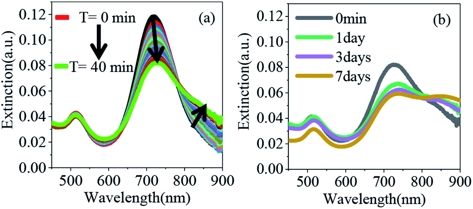 | ||
| Fig. 2 (a) Extinction spectra of PE coated gold nanorods in acetonitrile after addition of 5 μM of 1,6-hexanedithiol (in the presence of HCl) as a function of time. The black curve shows the extinction spectra of gold nanorods prior to HCl and thiol addition. (b) Extinction spectra of gold nanorods after addition of 35 mM Et3N. | ||
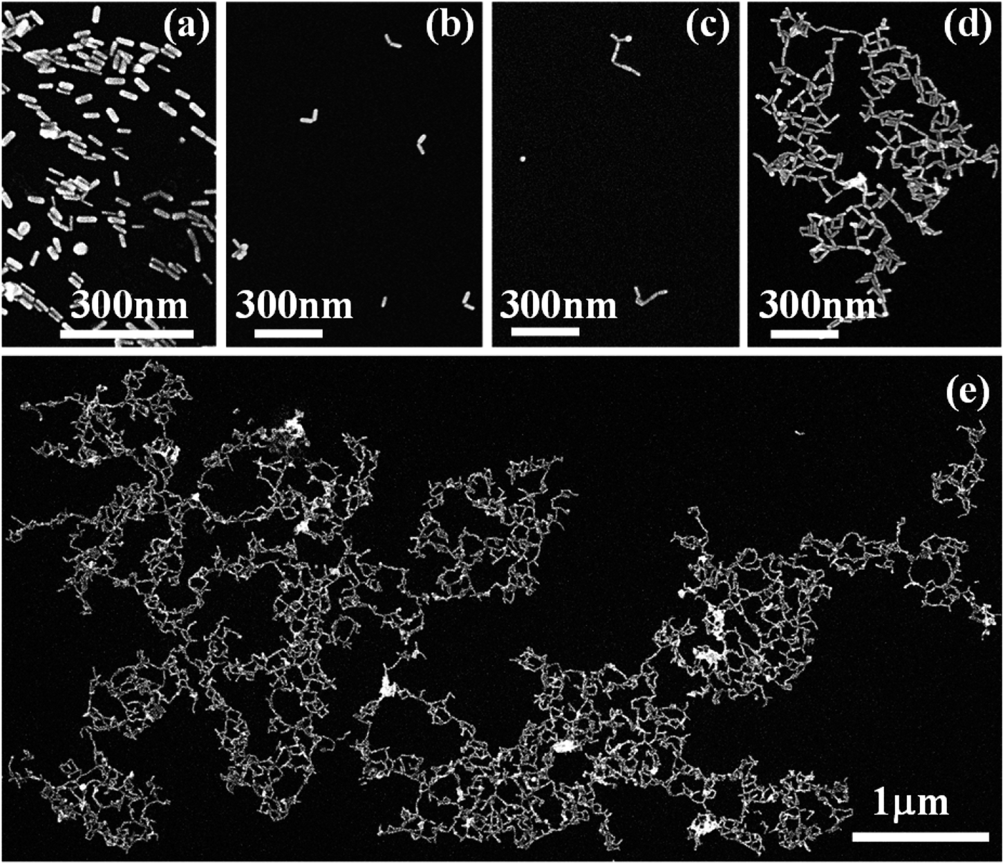 | ||
| Fig. 3 SEM images showing the growth of nanorod self-assemblies: (a) PAA overcoated gold nanorods (b) after 40 minutes of 1,6-hexanedithiol addition. (c–e) After 1 day, 3 days, and 7 days of Et3N addition. Note that for SEM imaging, samples were spin coated onto a silicon wafer to minimize aggregation due to solvent evaporation. | ||
We note that the initial tip-specificity in end-to-end dimers did not lead to formation of larger end-to-end linked assemblies over time. SEM images taken after 2 hours showed formation of only random aggregates (Fig. S4†). We believe that the loss of tip-specificity is a result of increased instability of the nanorods in acetonitrile due to reduction of nanorod's surface charge in the presence of HCl. With the decrease of the nanorods' surface charge, they face less interparticle repulsive force which is necessary to keep them isolated in solution.28
Importantly, the tip-specificity was maintained during the assembly growth process and large end-to-end linked nanorod assemblies were synthesized by increasing the magnitude of the nanorod surface charge via addition of excess Et3N within the first 30–40 minutes of aggregation. Increased surface charge results in a stronger electrostatic repulsion among nanorods and thereby prevents non-specific aggregation. Extinction spectra measured for up to 7 days showed a gradual decrease in the nanorod LSPR intensity associated with concurrent increase of the longer-wavelength broad peak intensity indicating slow growth of the assembly (Fig. 2b). Indeed, SEM images taken at different time intervals (Fig. 3c: 1 day, Fig. 3d: 3 days, and Fig. 3e: 7 days) clearly showed the growth of self-assembled nanostructures from dimers to large polymeric assemblies containing up to several thousands of individual nanorods (Fig. S10–S12†). Particularly impressive was the long-range tip specificity, which to the best of our knowledge, has not been achieved previously with gold nanorods (Fig. S10–S12†). Moreover, these assemblies were found to be stable in acetonitrile for over one month (Fig. S5†).
We note that the assembly formation was not due to solvent evaporation but the individual nanorods being linked by dithiol moieties. This is supported by the fact that no assembly formation was observed in the absence of dithiol under the same experimental conditions. Additionally, the measured gap dimensions from high-resolution transmission electron microscopy (TEM) images were found to be approximately 0.9 ± 0.2 nm (measured over 15 nanogaps, few examples are shown in Fig. S6†), which is consistent with the dimension of dithiol molecules.
Finally, the plasmonic hot spots in a gold nanorod assembly were used to enhance the fluorescence signal from a weak fluorophore, crystal violet (CV). Few groups have previously used CV molecules owing to their low fluorescence quantum yield and favorable spectral overlap with the nanorod plasmon.3,5,9,36 To probe the maximum fluorescence enhancement, we followed a previously developed method where a CV molecule dissolved in a highly viscous medium (glycerol) diffuses slowly through the plasmonic hot spots and occasionally passes through an optimum position generating strong intensity burst in the fluorescence time trace.
A gold nanorod assembly was isolated on an ITO-coated glass coverslip via spin coating (Fig. 4a). The same nanostructure was identified with our optical microscope (schematic of the setup is shown in Fig. S7†) by probing its photoluminescence signal (Fig. 4b). Fluorescence time traces recorded on different areas of the nanorod assembly showed strong fluorescence bursts. Fig. 4c (red trace) shows a typical fluorescence time trace (more traces are shown in Fig. S8†) taken on the nanorods assembly (diffraction-limited excitation area is shown in a red circle; the excitation wavelength was 633 nm). A background signal of ∼90000 counts per second originated from the inherent photoluminescence signal of the nanostructure and all the CV molecules (∼60 molecules in 1 fL focal volume) present in the focal volume. A fluorescence time trace measured on an area where no nanostructures were present (blue trace in Fig. 4c) showed an average fluorescence signal of ∼10000 counts per second yielding an average emission rate of ∼166 counts per s per CV molecule. The maximum intensity of fluorescence burst shown in Fig. 4c was found to be 1.649 × 10⁶ counts per second corresponding to an increase of 1.639 × 10⁶ counts per second coming from an enhanced CV molecule. Based on the fact that an unenhanced CV molecule generated fluorescence at 166 counts per second, we estimate a fluorescence enhancement factor of 9874. Time traces taken on different areas of the same nanostructures (Fig. S8†) yielded an average enhancement factor of (1.05 ± 0.17) × 104. We note that fluorescence enhancements achieved here are significantly larger than those of end-to-end dimers obtained via lithography35 or via DNA origami11 and are comparable to those of the state-of-the-art in-plane antenna arrays.36 Under the same experimental conditions, a single nanorod yielded a much weaker enhancement factor of 1221 (time trace shown in the inset in Fig. 4c), which is consistent with previous reports.9
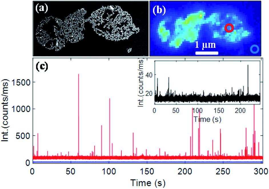 | ||
| Fig. 4 (a) SEM and (b) one-photon luminescence images of a gold nanorod assembly isolated on an ITO-coated glass substrate and covered with 100 nM CV in glycerol. (c) Fluorescence time traces recorded on a diffraction-limited spot (red circle) on the nanorod assembly (red) and at a place where no nanostructure was present (blue). The inset in (c) shows a typical fluorescence time trace taken on a single gold nanorod. A 633 nm laser was used as the excitation source. Excitation power was 0.8 mW (measured at the back of the objective). | ||
A plasmonic nanostructure is known to enhance the rate of fluorescence of an emitter located in its close proximity.41,42 Such enhancement is a result of both excitation and emission enhancements. A plasmonic nanostructure can act as an antenna for visible light and concentrates the incident electromagnetic field in a tiny area near its surface. Such a concentrated field leads to an enhanced light absorption by a molecule located within the plasmonic near-field. The nanostructure antenna can also increase the emission rates of a molecule. Both these enhancements depend on multiple factors including the local field enhancement created by the nanostructure and the distance and the relative orientation between the nanostructure and the emitter.3,43 For single gold nanorods, the field intensity enhancement is typically a few hundred fold. This can enhance the excitation rate by a few hundred times and the emission rate by a similar factor (although the increase of the non-radiative rate affects the overall fluorescence yield enhancement). The field intensity enhancement is even stronger for nanorod assemblies, especially when the nanorods are aligned in an end-to-end configuration and can reach up to 10000-fold.7 The higher fluorescence enhancement obtained for nanorod assemblies is likely to be a result of higher field enhancements at the nanogaps. Additionally, to demonstrate the plasmonic origin of the fluorescence enhancement we compared the fluorescence time traces measured on the same nanostructure (given in Fig. 4c) with 633 nm and 532 nm excitation, where the field enhancement is expected to be significantly low. The results are shown in Fig. S13.† The absence of strong fluorescence intensity bursts with 532 nm excitation supports that the enhancement is related to plasmonic field enhancement. This finding is also consistent with previous studies on the gold nanorod-crystal violet system, which indicated that the fluorescence enhancement was due to plasmonic near-field enhancements.3,5,9,44 Detailed theoretical calculations and fluorescence lifetime measurements will be required to quantitatively estimate the excitation and emission enhancement factors and will be carried out separately.
Conclusions
In conclusion, here we establish nanorod's surface charge as a key control parameter directing the growth of end-to-end attached gold nanorod assemblies linked via short dithiols. Long-range tip-specificity over thousands of gold nanorods was achieved via in situ tuning of nanorod's surface charge. We have also shown that these end-to-end assemblies can strongly enhance the fluorescence signal of a weak emitter by approximately ten-thousand fold, which is comparable to the largest reported fluorescence enhancement factor achieved in more expensive lithographically made in-plane antenna arrays. We note that the fluorescence enhancement factors reported here are still underestimated due to poor spectral overlap between the dye and the plasmonic nanostructure. Further improvements including the application of a NIR dye having a better spectral overlap with the coupled plasmon modes of the plasmonic network and NIR resonant excitations will be studied in the near future. To the best of our knowledge, the long-range tip specificity in gold nanorod assemblies has not been reported yet and will pave the way for the development of efficient plasmonic substrates with large hot-spot densities for SERS and MEF studies.Conflicts of interest
There are no conflicts to declare.Acknowledgements
We acknowledge financial support from Science and Engineering Research Board, India (project: EMR/2015/0013) and a seed grant from IIT Gandhinagar. We thank Dr Arnab Dutta (IIT Gandhinagar) and Prof. Michel Orrit (Leiden University) for many fruitful discussions. AK would like to acknowledge Pravin Hivare for assistance with AFM imaging.Notes and references
- P. Zijlstra and M. Orrit, Rep. Prog. Phys., 2011, 74, 106401 CrossRef.
- R. A. Alvarez-puebla, A. Agarwal, P. Manna, B. P. Khanal and P. Aldeanueva-potel, Proc. Natl. Acad. Sci. U. S. A., 2011, 108, 8157–8161 CrossRef CAS PubMed.
- S. Khatua, P. M. R. Paulo, H. Yuan, A. Gupta, P. Zijlstra and M. Orrit, ACS Nano, 2014, 8, 4440–4449 CrossRef CAS PubMed.
- P. Biagioni, J.-S. Huang and B. Hecht, Rep. Prog. Phys., 2012, 75, 024402 CrossRef PubMed.
- L. Su, H. Yuan, G. Lu, S. Rocha, M. Orrit, J. Hofkens and H. Uji-I, ACS Nano, 2016, 10, 2455–2466 CrossRef CAS PubMed.
- A. S. De Silva Indrasekara, B. Shuang, F. Hollenhorst, B. S. Hoener, A. Hoggard, S. Chen, E. Villarreal, Y. Y. Cai, L. Kisley, P. J. Derry, W. S. Chang, E. R. Zubarev, E. Ringe, S. Link and C. F. Landes, J. Phys. Chem. Lett., 2017, 8, 299–306 CrossRef CAS PubMed.
- G. Baffou and R. Quidant, Chem. Soc. Rev., 2014, 43, 3898–3907 RSC.
- C. Sönnichsen, T. Franzl, T. Wilk, G. Von Plessen, J. Feldmann, O. Wilson and P. Mulvaney, Phys. Rev. Lett., 2002, 88, 1–4 CrossRef PubMed.
- H. Yuan, S. Khatua, P. Zijlstra, M. Yorulmaz and M. Orrit, Angew. Chem., Int. Ed., 2013, 52, 1217–1221 CrossRef CAS PubMed.
- I. Haidar, G. Lévi, L. Mouton, J. Aubard, J. Grand, S. Lau-Truong, D. R. Neuville, N. Félidj and L. Boubekeur-Lecaque, Phys. Chem. Chem. Phys., 2016, 18, 32272–32280 RSC.
- T. Zhang, N. Gao, S. Li, M. J. Lang and Q. H. Xu, J. Phys. Chem. Lett., 2015, 6, 2043–2049 CrossRef CAS PubMed.
- A. Kinkhabwala, Z. Yu, S. Fan, Y. Avlasevich, K. Müllen and W. E. Moerner, Nat. Photonics, 2009, 3, 654–657 CrossRef CAS.
- D. Punj, M. Mivelle, S. B. Moparthi, T. S. Van Zanten, H. Rigneault, N. F. Van Hulst, M. F. García-Parajó and J. Wenger, Nat. Nanotechnol., 2013, 8, 512–516 CrossRef CAS PubMed.
- G. Han, D. Weber, F. Neubrech, I. Yamada, M. Mitome, Y. Bando, A. Pucci and T. Nagao, Nanotechnology, 2011, 22, 275202 CrossRef CAS PubMed.
- G. Zoriniants and W. L. Barnes, New J. Phys., 2008, 10, 105002 CrossRef.
- L. Vigderman, B. P. Khanal and E. R. Zubarev, Adv. Mater., 2012, 24, 4811–4841 CrossRef CAS PubMed.
- S. Pal, Z. Deng, H. Wang, S. Zou, Y. Liu and H. Yan, J. Am. Chem. Soc., 2011, 133, 17606–17609 CrossRef CAS.
- S. M. H. Abtahi, N. D. Burrows, F. A. Idesis, C. J. Murphy, N. B. Saleh and P. J. Vikesland, Langmuir, 2017, 33, 1486–1495 CrossRef CAS.
- Z. Nie, D. Fava, E. Kumacheva, S. Zou, G. C. Walker and M. Rubinstein, Nat. Mater., 2007, 6, 609–614 CrossRef CAS.
- Z. Nie, D. Fava, M. Rubinstein and E. Kumacheva, J. Am. Chem. Soc., 2008, 130, 3683–3689 CrossRef CAS PubMed.
- K. Liu, A. Lukach, K. Sugikawa, S. Chung, J. Vickery, H. Therien, B. Yang, M. Rubinstein and E. Kumacheva, Angew. Chem., Int. Ed., 2014, 53, 2648–2653 CrossRef CAS PubMed.
- Z. Sun, W. Ni, Z. Yang, X. Kou, L. Li and J. Wang, Small, 2008, 4, 1287–1292 CrossRef CAS PubMed.
- C. Wang, Y. Chen, T. Wang, Z. Ma and Z. Su, Chem. Mater., 2007, 19, 5809–5811 CrossRef CAS.
- J. Y. Chang, H. Wu, H. Chen, Y. C. Ling and W. Tan, Chem. Commun., 2005, 1092–1094 RSC.
- M. Grzelczak, J. Vermant, E. M. Furst and L. M. Liz-marza, ACS Nano, 2010, 4, 3591–3605 CrossRef CAS.
- L. Wang, Y. Zhu, L. Xu, W. Chen, H. Kuang, L. Liu, A. Agarwal, C. Xu and N. A. Kotov, Angew. Chem., Int. Ed., 2010, 49, 5472–5475 CrossRef CAS.
- S. T. S. Joseph, B. I. Ipe, P. Pramod and K. G. Thomas, J. Phys. Chem. B, 2006, 110, 150–157 CrossRef CAS PubMed.
- P. Pramod and K. G. Thomas, Adv. Mater., 2008, 20, 4300–4305 CrossRef CAS.
- W. Ni, R. A. Mosquera, P. Jorge and L. M. Liz-marz, J. Phys. Chem. Lett., 2010, 1, 1181–1185 CrossRef CAS.
- Y. Wang, A. E. Deprince, S. K. Gray, X. M. Lin and M. Pelton, J. Phys. Chem. Lett., 2010, 1, 2692–2698 CrossRef CAS PubMed.
- F. C. M. Leung, S. Y. L. Leung, C. Y. S. Chung and V. W. W. Yam, J. Am. Chem. Soc., 2016, 138, 2989–2992 CrossRef CAS PubMed.
- I. Haidar, J. Aubard, G. Lévi, S. Lau-Truong, L. Mouton, D. R. Neuville, N. Félidj and L. Boubekeur-Lecaque, J. Phys. Chem. C, 2015, 119, 23149–23158 CrossRef CAS.
- K. K. Caswell, J. N. Wilson, U. H. F. Bunz and C. J. Murphy, J. Am. Chem. Soc., 2003, 125, 13914–13915 CrossRef CAS PubMed.
- D. Zhao, Z. Zhang, Y. Wen, X. Zhang and Y. Song, Appl. Phys. Lett., 2013, 102, 123101 CrossRef.
- O. L. Muskens, V. Giannini, J. A. Sánchez-Gil and J. Gómez Rivas, Nano Lett., 2007, 7, 2871–2875 CrossRef CAS PubMed.
- V. Flauraud, R. Regmi, P. M. Winkler, D. T. L. Alexander, H. Rigneault, N. F. van Hulst, M. F. García-Parajo, J. Wenger and J. Brugger, Nano Lett., 2017, 17, 1703–1710 CrossRef CAS PubMed.
- B. Nikoobakht and M. A. El-Sayed, Chem. Mater., 2003, 15, 1957–1962 CrossRef CAS.
- T. K. Sau and C. J. Murphy, Langmuir, 2004, 20, 6414–6420 CrossRef CAS PubMed.
- A. M. Alkilany, L. B. Thompson and C. J. Murphy, ACS Appl. Mater. Interfaces, 2010, 2, 3417–3421 CrossRef CAS PubMed.
- J. Huang, J. Park, W. Wang, C. J. Murphy and D. G. Cahill, ACS Nano, 2012, 7, 589–597 CrossRef PubMed.
- T. Ming, H. Chen, R. Jiang, Q. Li and J. Wang, J. Phys. Chem. Lett., 2012, 3, 191–202 CrossRef CAS.
- F. Tam, G. P. Goodrich, B. R. Johnson and N. J. Halas, Nano Lett., 2007, 7, 496–501 CrossRef CAS PubMed.
- K. Munechika, Y. Chen, A. F. Tillack, A. P. Kulkarni, I. J. La Plante, A. M. Munro and D. S. Ginger, Nano Lett., 2010, 10, 2598–2603 CrossRef CAS PubMed.
- Y. Wang, M. Horáček and P. Zijlstra, J. Phys. Chem. Lett., 2020, 11, 1962–1969 CrossRef CAS PubMed.
Footnote |
| † Electronic supplementary information (ESI) available: Description of Experimental details, control experiments, additional SEM and TEM images, optical microscopy setup and fluorescence time traces. See DOI: 10.1039/d0na00303d |
| This journal is © The Royal Society of Chemistry 2020 |