DOI:
10.1039/D0MH00706D
(Communication)
Mater. Horiz., 2020,
7, 2390-2398
Real-time monitoring of trap dynamics reveals the electronic states that limit charge transport in crystalline organic semiconductors†
Received
28th April 2020
, Accepted 24th June 2020
First published on 24th June 2020
Abstract
Organic semiconductors (OSCs) have the potential to become ubiquitous in our lives as part of various optoelectronic devices given their low-cost processing, light weight, and the opportunities that they offer for designing new materials with “on demand” properties. Many OSCs have achieved remarkable performances, however, a complete understanding of the fundamental processes that govern their properties is still lacking. One such process is charge carrier trapping, a phenomenon that profoundly impacts the performance and stability of devices. Here we report on a comprehensive study on the physics of traps resulting from microstructure changes by monitoring the generation/annihilation of traps in 2,8-difluoro-5,11-bis(triethylsilylethynyl)anthradithiophene (diF-TES ADT), a high-mobility small molecule OSC. The variations in charge carrier mobility measured in organic field-effect transistors (OFETs) deliberately exposed to solvent vapor are correlated with the density and energetic distribution of the electronic states in the band gap of the OSC in all intermediate states of the microstructural transformations. Given the strong dependence of the electrical properties on the film microstructure, such information is instrumental in identifying performance-limiting processes in devices and subsequently guiding material processing to achieve intrinsic limits. The discovery of defect-tolerant intermediate crystalline motifs may provide new pathways for fabricating stable, high-performance devices for next-generation low-cost electronics.
New concepts
Organic semiconductors can become ubiquitous in optoelectronics given their low-cost processing and compatibility with flexible substrates – properties arising from their weak intermolecular interactions. Unfortunately, these interactions also make them susceptible to defect formation: localized electronic states can trap charge carriers, a phenomenon that profoundly impacts the performance and stability of devices. Here, we probe for the first time the transformations in the density and energetic landscape of electronic traps during microstructure evolution in organic semiconductor films. Monitoring in real-time the trap density of states gave us unprecedented access to the complex structural dynamics occurring in high-mobility materials and the underpinning structure–property relationships. Given the strong dependence of electrical properties on the film microstructure, such measurements are instrumental in identifying performance-limiting processes in optoelectronic devices and subsequently guiding material processing to achieve intrinsic limits. Our results simultaneously provide the electrical properties and the energetic distribution of traps of all intermediate states during the microstructural transformations. Access to such information brings an important new perspective to understanding the fundamental processes governing charge transport in organic semiconductors and may result in the discovery of defect-tolerant intermediate crystalline motifs that can be selectively frozen in to achieve efficient devices.
|
Introduction
Organic semiconductors (OSCs) are gaining attention for incorporation in the next-generation flexible, bendable and stretchable optoelectronic devices. Key attributes that make them attractive are their low-cost processing, lightweight, tunability of properties, and compatibility with flexible substrates.1–5 These properties are a direct consequence of the weak intermolecular interactions inherent in these materials, but unfortunately these interactions also make OSCs susceptible to defect formation. Localized electronic states introduced in the band gap can trap charge carriers, a phenomenon that has a profound impact on the mechanism of charge transport, as well as on the performance and stability of optoelectronic devices.6–14 Hence, their detection and characterization is crucial to understanding performance-limiting processes, and subsequently guiding the processing and handling that is necessary for engineering high-performance optoelectronic devices.1,6,9,15–19 Several experimental tools are available for this purpose, including optical, thermal and electrical methods that provide access to the density, spatial and energetic distribution of traps.12,20–23 In particular, the energetic distribution of traps, also referred to as the trap DOS spectrum, provides information about the distribution of electronic states as a function of energy within the band gap of the OSC.22,24–27 Access to this information has yielded improvements in device performance and reliability. For example, new material design rules have been proposed to enable trap-free charge transport in OSCs.28 The nature of device interfaces has been re-evaluated in order to reduce trap formation during operation of organic field-effect transistors (OFETs),29 and molecular additives have been incorporated into polymer films to enhance the electrical stability of organic diodes.8 Systematic studies where traps are deliberately introduced into the OSCs to examine their effect on the DOS spectrum and device performance are very insightful as they can reveal the precise nature and origin of traps, provide a quantitative understanding of their effects, and therefore guide device design and film processing by pinpointing the phenomena that could lead to more trap-tolerant systems. However, only a few such studies have been reported. For example, the effect of O2 exposure,30 X-ray irradiation,8 proton and He+ irradiation,31 on the DOS spectrum of OSCs have been studied.
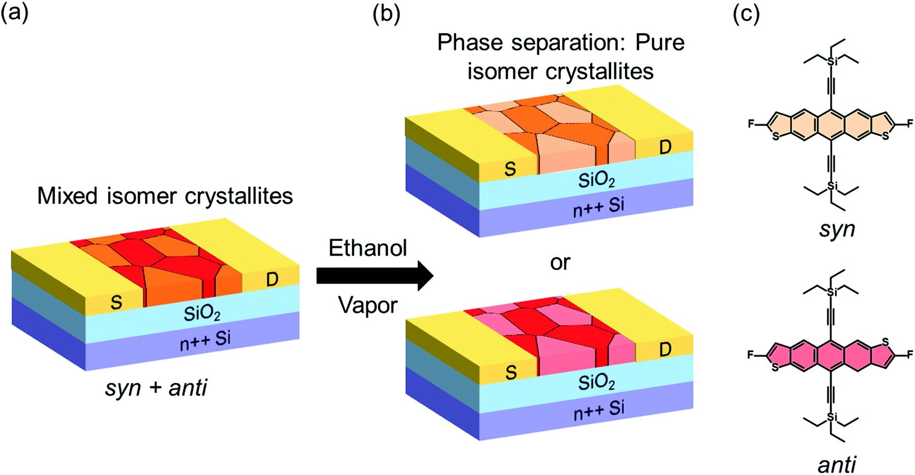
Here we monitored in real time the generation and annihilation of traps in OSCs in response to microstructural changes and percolation of impurity centres, and examined the resulting impact on the performance of OFETs. The devices were deliberately exposed to solvent vapor and we probed the density and energetic landscape of electronic traps of all intermediate states during the microstructural transformation. The measurements provided access to the dynamics of trap formation and healing as a result of the complex processes taking place within the OSC upon interaction with the solvent. We focused on 2,8-difluoro-5,11-bis(triethylsilylethynyl)anthradithiophene (diF-TES ADT), a small molecule OSC that has demonstrated remarkable electrical properties, with mobilities greater than 10 cm2 V−1 s−1 in optimized devices with near ideal current–voltage characteristics.32,33 diF-TES ADT has two isomers: syn and anti (see molecular structures in Fig. 1); the material typically consists of a 40–60 isomeric mixture. The coexistence of isomers in the transistor channel introduces a peak in the DOS spectrum at ca. 0.3–0.4 eV from the valence band edge, corresponding to deep traps responsible for the reduced device performance when compared to isomerically pure samples, where the peak is absent.34 The isomers can be separated through elaborate synthetic procedures,35,36 or meticulous processing.34 Recently, polarized Micro Raman spectroscopy measurements indicated that the syn and anti isomers phase-segregate into pure-isomer crystalline grains that coexist intimately in the transistor channel of mix-isomer films.37 Hence, the devices can be of two types, depending on the distribution of grains across the transistor channel. The first type consists of a mixture of syn and anti crystalline grains, as illustrated in Fig. 1a, and the second contains only grains of one isomer type in the channel: either only syn (top panel of Fig. 1b) or only anti (bottom panel of Fig. 1b). Consequently, the mix-devices exhibit a peak in the trap DOS spectrum, while the pure isomer devices do not, and hence we will use the presence/absence of the peak as a way to distinguish between the two device types in order to individually monitor the response of these devices when exposed to a solvent vapor. We discovered that exposing an OFET containing a film of isomer mixture to ethanol vapor induces a phase separation of the two isomers via reorganization of molecules in the transistor channel, which is detected as a gradual reduction in intensity, followed by the disappearance of the peak in the DOS spectrum. In addition, a reduction in the overall density of states was also evident, resulting from microstructural rearrangement of the film in the process of reaching thermodynamic equilibrium. Correspondingly, a 30% increase in charge carrier mobility was observed during the time of exposure. On the other hand, in devices with pure isomer crystallites, exposure to the solvent vapor generated band gap states manifested in the DOS spectrum as a peak centered at ca. 0.22 eV from the valence band edge, likely originating form impurity centers percolating into the film. The generation of these states results in a decrease in the device mobility by 20%.
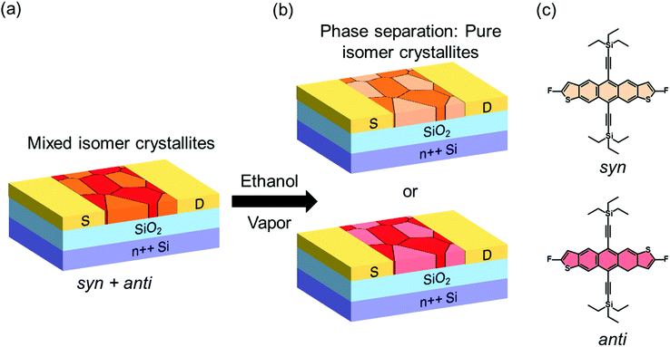 |
| | Fig. 1 diF-TES ADT OFET device structure and film modifications during exposure to ethanol vapor. (a) Device consisting of a mixture of syn and anti isomer crystalline grains in the transistor channel between the source (S) and drain (D) electrodes. (b) A phase separation occurs upon exposure to ethanol vapor and each isomer re-crystallizes into grains consisting of pure syn (top) or pure anti (bottom) isomers. Shades of orange and red are used to symbolize different orientations of individual grains of syn and anti isomers, respectively. (c) The molecular structures of syn (top) and anti (bottom) isomers of diF-TES ADT. | |
Experimental
OFETs were fabricated in the bottom-gate, bottom-contact geometry with a heavily doped n-type Si wafer and a 200 nm thermally grown SiO2 layer serving as the gate and the gate dielectric, respectively. A 3 nm Ti layer followed by a 40 nm Au layer was evaporated through a shadow mask to define the source and the drain electrodes. The prefabricated substrates were treated with pentafluorobenzenethiol (PFBT) self-assembled monolayer to improve charge injection and film microstructure.32 A 1.5 wt% solution of a 40/60 diF-TES ADT isomeric mixture in room-temperature chlorobenzene was then spin coated onto the prefabricated substrate according to the procedure reported elsewhere.32 The resulting film thickness was ∼60 nm. Electrical measurements were performed using an Agilent 4155 C parameter analyzer under an inert N2 or N2/ethanol vapor (for measurements obtained during ethanol exposure) environment. Room-temperature anhydrous (histological grade) ethanol from Fisher scientific Inc. was used as purchased, with no further treatment. The exposure of OFETs to ethanol vapor was performed in a nitrogen atmosphere and in dark.
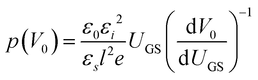
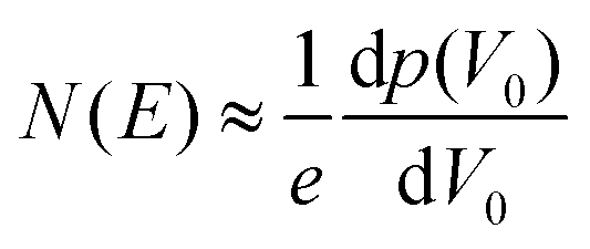
In order to access the trap DOS spectrum, we employed Grünewald's model, which uses the linear-regime transfer characteristics of an OFET (drain current ID as a function of gate-source voltage VGS at a low, fixed drain-source voltage VDS) to extract the trap DOS as a function of energy from the valence band edge.38–40 Here, we briefly outline the essential steps necessary to perform the analysis. First, the interface potential at the OSC/dielectric interface (V0) is obtained as a function of gate-source voltage above flat-band (UGS = VGS − VFB) by numerically solving the following equation:
| |  | (1) |
where
εi and
l are the relative permittivity and the thickness of the dielectric, respectively,
εs and
d are the relative permittivity and the thickness of the semiconductor, respectively,
σ(
UGS) is the field-effect conductivity (evaluated from the linear regime transfer characteristics) and
σ0 is the conductivity at flat band voltage, assumed to be the turn-on voltage (
VON) of the device. The function
V0(
UGS) is used to determine the total whole density from,
| |  | (2) |
The trap DOS is then obtained by numerically differentiating the total hole density with respect to V0. i.e.,
| |  | (3) |
where
E = e
V0 is the energy of the trapping state w.r.t the Fermi level. diF-TES ADT yields p-channel OFETs and hence in these measurements we access electronic states above the valence band edge. The result is the trap DOS spectrum as a function of energy in the bandgap of the OSC.
Results and discussion
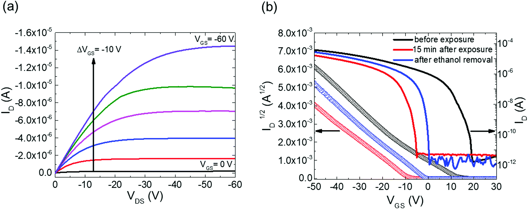
Fig. 2a shows the output characteristics of a device consisting of mixed isomers (IDvs. VDS at various fixed VGS) obtained before exposure to the solvent vapor. These characteristics are near-ideal, as indicated by the linearity of the curves at low VDS and clear saturation attained at high VDS. The absence of S-shaped current–voltage curves close to VDS = 0 is an indication of low contact resistance.32,41 In Fig. 2b we include the transfer characteristics in the saturation regime (IDvs. VGS at VGS = −60 V) before exposure to ethanol vapor (black), after 15 min into exposure (red), and immediately after the ethanol container was removed (blue). Clearly, the exposure to solvent vapor is inducing a significant change in the current–voltage characteristics. Intrigued by these experimental observations, we monitored in situ how the trap DOS spectrum evolves during exposure to the solvent vapor. To perform this analysis, the devices were first measured under N2 and then an open jar (diameter ∼1.5 cm) of ethanol was transferred into the measurement chamber and the linear-regime transfer characteristics were recorded immediately, at regular time intervals of 15 s, for a duration of 15 min. The DOS spectra were evaluated following the procedure described above.
 |
| | Fig. 2 Current–voltage characteristics of a diF-TES ADT OFET device exposed to solvent vapor. (a) IDvs. VDS plot at various fixed VGS (0 V to −60 V in −10 V increments) measured before exposure to the ethanol vapor. (b) IDvs. VGS plot at VDS = −60 V obtained before exposure to ethanol vapor (black), after 15 min of exposure (red) and after removal of ethanol from the measurement chamber (blue). The left and right axes show the square root and logarithm of the drain current, respectively. | |
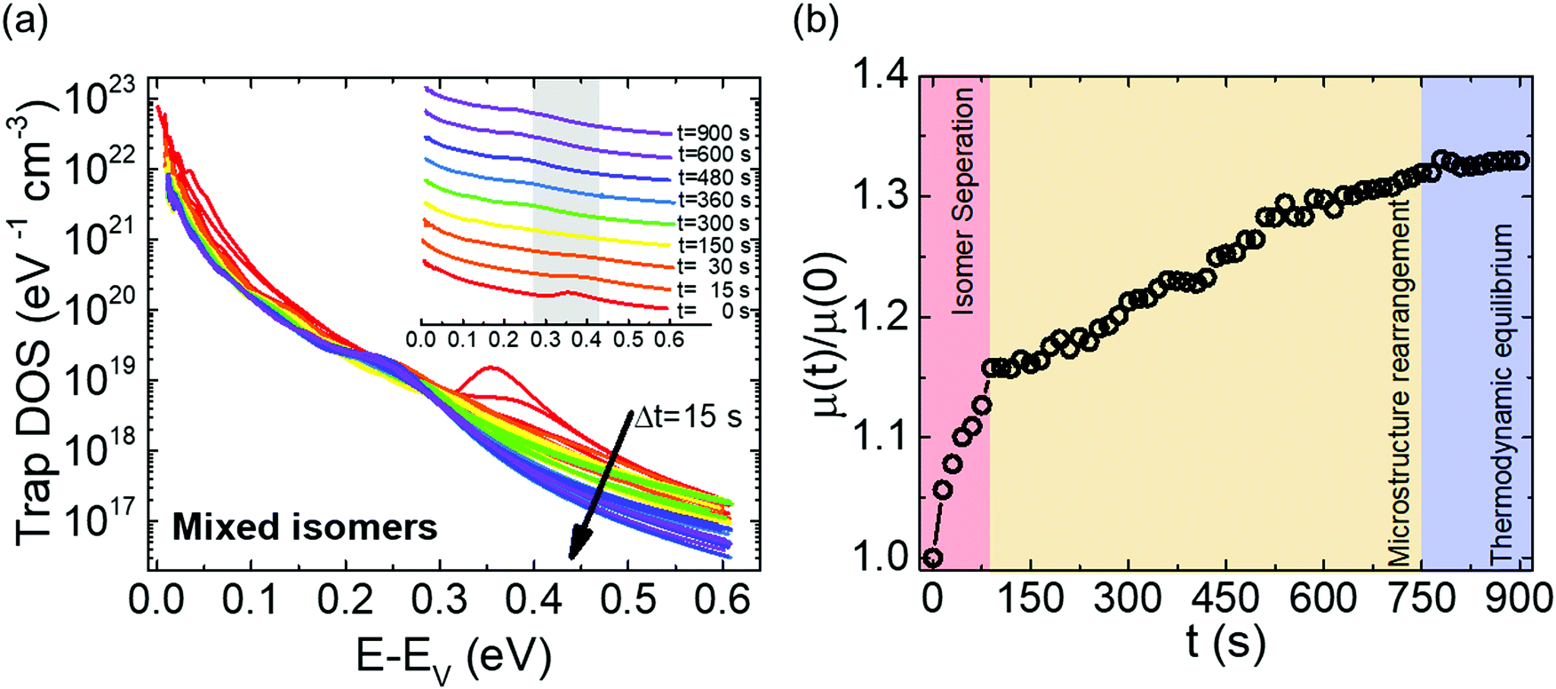
In Fig. 3a, we plot the time evolution of the trap DOS spectrum of a device consisting of mixed isomers when exposed to ethanol vapor. The function V0(UGS) is included in Fig. S1 in ESI.† Before exposure, i.e., at t = 0 s (red curve), the spectrum resembles an exponential DOS close to the valence band edge, with a peak at 0.36 eV, reminiscent of a device with mixed isomer crystalline grains in the channel (Fig. 1a). While exponential DOS are generally associated with disorder in the film originating form thermal molecular motions and structural defects, a peak in the DOS spectrum is due to discrete electronic states in the bandgap, originating from chemical impurities or a predominant defect.6 In our measurements, the peak arises due to deep traps originating from the presence of one isomer in the host crystal of the other, details on the mechanism of trapping were discussed elsewhere.34 After 15 s of exposure (orange curve), the amplitude of the peak diminishes and the peak is completely annihilated at t = 30 s. We attribute this transformation to a gradual isomer separation, facilitated by a modification of the film microstructure in the presence of ethanol vapor. Ethanol molecules interact with the OSC film, promoting molecular rearrangement within the layer to reach a more energetically favorable state.42 The syn isomer is more polar in nature than the anti isomer and therefore it is possible that the polar ethanol molecules selectively extract the syn isomers from the film facilitating the isomer separation. While the phase separation is evident, the type of isomer accessed in our measurements is not clear due to the complex nature of this separation. Considering the vertical segregation, the polar SiO2 substrate would favour the assembly of the more polar isomer (syn) on its surface,34 however, the denser crystalline lattice of the anti-isomer would favour its accumulation on the bottom.35 A horizontal phase separation also occurs, leading to the formation of pure isomer crystalline sub-domains.37 Not surprisingly, but also confirmed by density functional theory (DFT) calculations, the lowest energy corresponds to isomer de-mixing,34 hence the film progresses towards isomerically pure crystallites (Fig. 1b) during solvent exposure. In fact, when measuring an array of OFET devices fabricated from a syn/anti mixture, we typically find that around 85% of devices consist only of one isomer, as indicated by the absence of a peak in the DOS spectrum, which is in agreement with the energy considerations. Upon further exposure to the solvent vapor, a reduction in the overall trap densities is also evident in the DOS spectrum (see the curves from orange to violet in Fig. 3a). Solvent–vapor annealing is known to cause microstructural rearrangement, allowing the film initially trapped kinetically in non-equilibrium states to attain thermodynamic equilibrium.43,44 A decrease in the overall trap densities is therefore attributed to molecular reorganization in the transistor channel to minimize the total potential energy until the system reaches thermodynamic equilibrium. Thus, these measurements, where we were able to monitor the reduction in the peak intensity followed by its disappearance, and then the minimization of the overall trap densities, gave us real-time insights into the dynamics of microstructural transformations occurring in the film containing mixed isomer crystalline grains. We discovered that reorganization of molecules in the transistor channel in the presence of solvent vapor is a two-step process: first, isomer separation occurs to minimize the total energy of the system, followed by a reduction in the crystalline defect density to reach the state of thermodynamic equilibrium. Structural rearrangement occurs within a minute of solvent exposure, similar to the case of TES ADT films.44
 |
| | Fig. 3 (a) Evolution of the trap DOS spectrum of a device with mixed isomer crystallites. The DOS curves are plotted as a function of energy from the valence band edge and clearly illustrate the annihilation of the peak at 0.36 eV. The DOS was evaluated every 15 s during exposure to ethanol vapor and the time evolution of the spectrum from t = 0 s (red) to t = 900 s (violet) is shown. Inset includes a subset of the trap DOS spectra offset for clarity. (b) Time evolution of the charge carrier mobility during the period of solvent exposure. The value is normalized to the initial value obtained before exposure to ethanol. | |
To obtain deeper insights into the trap parameters and how they alter after solvent exposure, we modeled the DOS spectra at t = 0 s and t = 900 s using two exponential functions to describe the distribution of shallow and deep states, respectively, with the addition of a Gaussian distribution to model the spectrum at t = 0 s according to the following equation:
| |  | (4) |
where
E1,
E2 are the characteristic decay energies and
N1,
N2 are the amplitudes of the respective exponential distributions,
Epeak defines the position of the Gaussian distribution with an amplitude
A and standard deviation
σ. The model parameters and fits to experimental data are summarized in
Table 1 and Fig. S2 in ESI,
† respectively. While the characteristic energy for the double exponential distributions remains the same over the course of ethanol exposure (∼21 meV for shallow states and ∼86 meV for deeper states), the density of shallow and deep states decreases by 65% and 12% respectively after 15 min of solvent exposure. The Gaussian distribution centered at 0.36 eV from the valence band edge represents the peak in DOS spectrum at
t = 0 s.
Table 1 Model parameters used for the double exponential and Gaussian distributions employed to model the DOS spectra of a device with mixed isomers. The spectrum at t = 900 s was modelled only using a double exponential distribution and therefore the Gaussian parameters are not applicable
| Model parameter |
t = 0 s |
t = 900 s |
|
N
1 (eV−1 cm−3) |
4.9 × 10²² |
1.7 × 10²² |
|
E
1 (meV) |
21.2 |
20.6 |
|
N
2 (eV−1 cm−3) |
2.5 × 10²⁰ |
2.2 × 10²⁰ |
|
E
2 (meV) |
85.5 |
85.5 |
|
A (eV−1 cm−3) |
1.0 × 10¹⁹ |
N/A |
|
E
peak (eV) |
0.36 |
N/A |
|
σ (meV) |
29.0 |
N/A |
In order to understand how the process of trap reduction influences the performance of devices, we monitored the evolution of the charge carrier mobility (μ), during the entire time of exposure to ethanol. The mobility was extracted from the slope of IDvs. VGS curve using the following equation,45
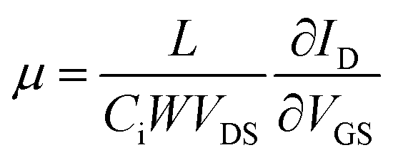
| |  | (5) |
where
L and
W are the length and width of the transistor channel,
Ci = 17.3 nF cm
−2 is the areal capacitance of the 200 nm thick SiO
2 dielectric. Mobilities of devices were in the order of 0.1 cm
2 V
−1 s
−1, on par with values reported on this material in OFETs with SiO
2 dielectric and in similar device architectures.
34,35 Higher mobilities are achievable with Cytop dielectric in the top-gate bottom-contact geometry due to reduced interfacial trap densities at the dielectric/semiconductor interface and lower contact resistance facilitated by the staggered device geometry.
29,35 Our choice of device type and geometry was motivated by the need to increase the sensitivity of trap detection by increasing the overall trap densities. Additionally, this architecture allows the film to better reorganize during solvent exposure without being constrained by the conformal dielectric and gate electrode on the top.
Fig. 3b shows the time evolution of the device mobility normalized to the initial value (at
t = 0 s). Three different regimes can be identified. In the first regime (shaded red region), a drastic increase in mobility is observed, which corresponds to the annihilation of the peak in the DOS spectrum resulting from solvent-induced isomer separation. The schematic in
Fig. 4 illustrates different snapshots of the energetic distribution of traps in the band gap over the course of ethanol exposure. Panel a corresponds to
t = 0 s, where deep states exist in the band gap, indicated in red, in addition to the shallow tail states shown in black. The density of deep states is reduced at
t = 15 s (
Fig. 4b) and they completely vanish at
t = 30 s (
Fig. 4c), as indicated by the disappearance of the peak in the DOS spectrum. In the second region of
Fig. 3b, enclosed by yellow shading, the mobility is increasing at a much slower rate, a phenomenon which is attributed to molecular reorganization in the transistor channel to minimize the total potential energy, which translates into a corresponding reduction in the overall trap densities evident in the DOS spectrum. This reduction is reflected in
Fig. 4d which depicts a decrease in the number of shallow tails states after exposure to the solvent vapor. Finally, in the third region in
Fig. 3b, bounded by blue shading (
i.e., after about 750 s), the mobility appears to have plateaued, indicating molecular assembly in the lowest potential energy configuration and that the system has reached thermodynamic equilibrium. In a previous study we have showed that such a stable configuration can be achieved by applying gentle vibrations during crystallization of the film.
34
 |
| | Fig. 4 Snapshots of the energetic distribution of localized band gap states at different times during microstructure reorganization in a device with mixed isomer grains: (a) t = 0 s, (b) t = 15 s, (c) t = 30 s and (d) t = 900 s. Shallow and deep states in the band gap are represented in black and red lines, respectively. | |
Since the above measurements were taken over short periods of time (15 s), it is likely that the device was under excessive bias stress. Bias stress effects can also induce charge carrier traps.6,46 Hence, there are, in fact, two possible contributions to the changes in the trap distribution observed above; bias stress and microstructure reorganization in the presence of ethanol vapor. In order to clarify the individual contribution of each, we performed several control experiments. First, characterization of devices based on mixed isomers was carried out in N2 under the same time intervals, but in the absence of ethanol, to eliminate the effect caused by the solvent vapor, results are shown in Fig. S3 in ESI.† Contrarily to the measurements performed under ethanol exposure, the peak in the DOS spectra persists, which confirms that bias stress is not responsible for the observed changes. In the second test experiment, the devices were exposed to ethanol vapor, but measurements were taken only before exposure and after 15 minutes, thus, ensuring that the devices were not stressed during the exposure; results are displayed in Fig. S4 in ESI.† The annihilation of the peak after 15 min of exposure in the absence of any bias stress unequivocally confirms that the changes observed in the DOS spectrum are solely caused by the effect of the solvent vapor. Also shown in the same plot is the DOS spectrum evaluated after the solvent was removed from the chamber following exposure (blue curve). The peak does not reappear after the jar of ethanol is removed, implying that once a device with mixed isomers transforms into the more stable device consisting only of one isomer, it remains in that state.
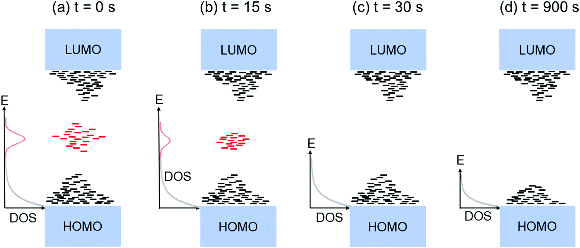
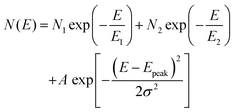
Next, we tested the response of devices consisting of pure isomer crystallites during exposure to ethanol vapor. Measurements were taken both on OFETs where the isomer separation took place during sample fabrication, as well as on solvent-annealed samples discussed above; the results were similar. Fig. 5a shows the DOS spectrum evaluated every 30 s over a course of 15 min. The function V0(UGS) is included in Fig. S5 of ESI.† Initially, the DOS spectra represent an exponential DOS with the absence of a peak (red curve). A snapshot of the trap distribution corresponding to this scenario is provided in Fig. S6a of ESI.† After t = 30 s, a progressive generation of a peak centered at 0.22 eV from the valence band edge is evident in the spectra. The establishment of the peak is initiated with a broadening of the DOS at t = 30 s, followed by a gradual increase in peak amplitude from t = 60 s to t = 900 s. The normalized mobility vs. time plot for the same device (Fig. 5b) shows a monotonic decrease in the mobility during the entire duration of exposure (an overall ∼20% decrease), correlating with the increasing amplitude of the peak observed in the DOS spectrum. Additional electronic states are generated in the band gap during the period of exposure to the solvent vapor (see Fig. S6b of ESI†), which were absent initially, explaining the creation of the peak in the DOS spectrum and therefore the decrease in mobility. Establishing the nature of the trap giving rise to the peak is challenging since this appears to be a metastable state; the samples return to the initial “no-peak” state in a matter of seconds as soon as the ethanol vapor is removed. We do not exclude that a reverse modification of the film microstructure, where the molecules reorganize to form mixed isomer crystallites, occurs. Nevertheless, it should be noted that the trap depth of the electronic states generated is different from that in the earlier case of 0.36 eV. Additionally, since this device type is already in its lowest energy configuration, which corresponds to a state where the isomers are separated, the energy penalty necessary to convert it to the less stable configuration of a device consisting of mixed isomer grains would be significant. Hence, this scenario is highly unlikely, and the peak probably originated from a different source. One such likelihood is that ethanol (or the impurities present in it), upon percolation into the film, acts as an impurity center giving rise to discrete electronic states in the band gap, with depths that are dependent on the electric field induced by the dipole moment of the polar ethanol molecules.47 Trap parameters extracted by modeling the DOS spectra at t = 0 s and t = 900 s using eqn (4) are summarized in Table S1 in ESI,† and the fits to experimental spectra are provided in Fig. S7 of ESI.† The densities of both shallow and deep states do not change significantly over the course of ethanol exposure, however, the increase in the characteristic decay energy of both shallow and deeps states indicates a broadening of the DOS. Such a broadening can take place when the crystal lattice is distorted due to the presence of impurity centers which introduces the peak in the DOS spectrum represented by the Gaussian centered at 0.22 eV. With new insights gained on the impact of impurity centres on the DOS, we took a closer look at the trap DOS spectrum of the mixed isomer device (Fig. 3a); it appears that a new peak centered around 0.2 eV begins to form after prolonged ethanol exposure (i.e., blue/purple curves at t >360 s), most likely due to the metastable impurity centers percolating into the film following isomer separation. Comparing Fig. 3a and 5a, the following can be inferred about the dynamics of trap annihilation vs. trap formation; the annihilation of traps due to isomer separation in mixed isomer films is a fast process and takes place within the first minute of exposure to ethanol vapor, while the formation of traps due to impurity centers occurs after about 5 min of ethanol exposure.
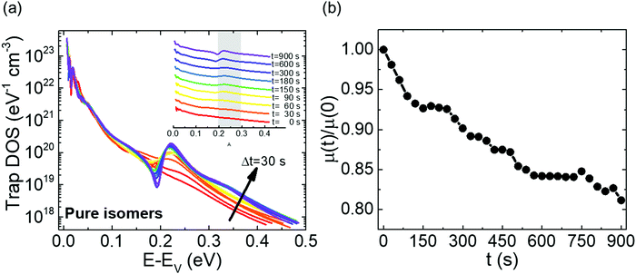 |
| | Fig. 5 (a) Evolution of the trap DOS spectrum of a device consisting of pure isomers. The DOS curves are plotted as a function of energy from the valence band edge and clearly illustrate the generation of a peak at 0.22 eV. The DOS was evaluated every 30 s during exposure to ethanol vapor and the time evolution of the spectrum from t = 0 s (red) to t = 900 s (violet) is shown. Inset shows a subset of the trap DOS spectra offset for clarity. (b) Time evolution of the charge carrier mobility during the period of solvent exposure. The value is normalized to the initial value obtained before exposure to ethanol. | |
Control experiments similar to those performed on mixed isomer devices were also carried out on this device type in order to confirm that the generation of the peak in DOS spectrum is solely induced by the interaction of the film with ethanol vapor and not a bias stress effect. The DOS spectra in Fig. S8 of ESI,† evaluated over the course of bias stress measurements show no evidence for the establishment of a peak. Similarly, the DOS spectra of a device with pure isomers shows the generation of a peak after 15 min of exposure in the absence of bias stress (Fig. S9, ESI†), confirming that such a peak was indeed caused by the effect of ethanol vapor. The absence of the peak in the DOS spectrum evaluated after the removal of the ethanol vapor (blue curve) suggests that such discrete trapping states are evident only in the presence of the solvent vapor and supports our earlier hypothesis of ethanol acting as a metastable impurity center.
Conclusions
In summary, we accessed in real time the generation and annihilation of charge carrier traps in a small molecule OSC and evaluated the resulting effect on charge transport. The traps originated from microstructure modifications or introduction of impurity centers upon exposure to a solvent vapor. A sharp increase/decrease in the charge carrier mobility of the devices exposed to ethanol vapor coincides with the elimination/formation of a predominant trap, as suggested by the gradual annihilation/generation of a peak in the DOS spectrum. A milder enhancement in mobility observed in mixed isomer devices correlates with the reduction in overall trap densities as a result of film reorganization to attain thermodynamic equilibrium. We were able to detect with high sensitivity all the intermediate processes occurring at different timescales during the generation/annihilation of electronic states in the band gap of the OSC, including the effects of film transformation from kinetically trapped to thermodynamically stable phases. These results provide access to a remarkable level of detail about the trap dynamics in high mobility OSCs and will not only be instrumental in identifying the processes that hinder the optimal functioning of electronic devices, but can also guide the development of sensing applications that function based on charge carrier trapping. The measurements also offer insights into how the mechanism of charge transport in OSCs is altered by the presence of traps, for example, elucidating the time evolution of band tail states caused by dynamic disorder, the major performance-limiting factor in electronic devices. This type of fundamental advance is instrumental in exploring new pathways for fabricating stable and high-performance devices for the next-generation of large-area and low-cost electronics.
Conflicts of interest
All authors declare no conflicts of interest.
Acknowledgements
This work was supported by National Science foundation through Grant No. DMREF-1627925 and DMREF-1627428.
References
- S. Fratini, M. Nikolka, A. Salleo, G. Schweicher and H. Sirringhaus, Nat. Mater., 2020, 19, 491–502 CrossRef CAS PubMed.
- H. Bronstein, C. B. Nielsen, B. C. Schroeder and I. McCulloch, Nat. Rev. Chem., 2020, 4, 66–77 CrossRef CAS.
- Y. Zhou, C. Fuentes-Hernandez, J. Shim, J. Meyer, A. J. Giordano, H. Li, P. Winget, T. Papadopoulos, H. Cheun, J. Kim, M. Fenoll, A. Dindar, W. Haske, E. Najafabadi, T. M. Khan, H. Sojoudi, S. Barlow, S. Graham, J.-L. Bredas, S. R. Marder, A. Kahn and B. Kippelen, Science, 2012, 336, 327–332 CrossRef CAS PubMed.
- B. Russ, A. Glaudell, J. J. Urban, M. L. Chabinyc and R. A. Segalman, Nat. Rev. Mater., 2016, 1, 16050 CrossRef CAS.
- J. Rivnay, S. Inal, A. Salleo, R. M. Owens, M. Berggren and G. G. Malliaras, Nat. Rev. Mater., 2018, 3, 17086 CrossRef CAS.
- H. F. Haneef, A. M. Zeidell and O. D. Jurchescu, J. Mater. Chem. C, 2020, 8, 759–787 RSC.
- M. Nikolka, I. Nasrallah, B. Rose, M. K. Ravva, K. Broch, A. Sadhanala, D. Harkin, J. Charmet, M. Hurhangee, A. Brown, S. Illig, P. Too, J. Jongman, I. McCulloch, J. Bredas and H. Sirringhaus, Nat. Mater., 2017, 16, 356–362 CrossRef CAS.
-
A. Salleo, Organic Electronics, Wiley-VCH Verlag GmbH & Co. KGaA, Weinheim, Germany, 2013, pp. 341–380 Search PubMed.
- M. F. Calhoun, C. Hsieh and V. Podzorov, Phys. Rev. Lett., 2007, 98, 096402 CrossRef CAS.
- A. A. Virkar, S. Mannsfeld, Z. Bao and N. Stingelin, Adv. Mater., 2010, 22, 3857–3875 CrossRef CAS PubMed.
- M. J. Ford, J. G. Labram, M. Wang, H. Wang, T.-Q. Nguyen and G. C. Bazan, Adv. Electron. Mater., 2017, 3, 1600537 CrossRef.
- A. Campos, S. Riera-Galindo, J. Puigdollers and M. Mas-Torrent, ACS Appl. Mater. Interfaces, 2018, 10, 15952–15961 CrossRef CAS PubMed.
- P. Westacott, N. D. Treat, J. Martin, J. H. Bannock, J. C. de Mello, M. Chabinyc, A. B. Sieval, J. J. Michels and N. Stingelin, J. Mater. Chem. A, 2017, 5, 2689–2700 RSC.
- J. Sayago, F. Soavi, Y. Sivalingam, F. Cicoira and C. Santato, J. Mater. Chem. C, 2014, 2, 5690–5694 RSC.
- G. Zuo, M. Linares, T. Upreti and M. Kemerink, Nat. Mater., 2019, 18, 588–593 CrossRef CAS.
- G. Zuo, Z. Li, O. Andersson, H. Abdalla, E. Wang and M. Kemerink, J. Phys. Chem. C, 2017, 121, 7767–7775 CrossRef CAS.
- H. Hirwa and V. Wagner, Org. Electron., 2015, 25, 112–120 CrossRef CAS.
- M. Nikolka, K. Broch, J. Armitage, D. Hanifi, P. J. Nowack, D. Venkateshvaran, A. Sadhanala, J. Saska, M. Mascal, S.-H. Jung, J. Lee, I. McCulloch, A. Salleo and H. Sirringhaus, Nat. Commun., 2019, 10, 2122 CrossRef PubMed.
- M. Nikolka, G. Schweicher, J. Armitage, I. Nasrallah, C. Jellett, Z. Guo, M. Hurhangee, A. Sadhanala, I. McCulloch, C. B. Nielsen and H. Sirringhaus, Adv. Mater., 2018, 30, 1801874 CrossRef PubMed.
- T. He, Y. Wu, G. D’Avino, E. Schmidt, M. Stolte, J. Cornil, D. Beljonne, P. P. Ruden, F. Würthner and C. D. Frisbie, Nat. Commun., 2018, 9, 2141 CrossRef PubMed.
- T. Hallam, M. Lee, N. Zhao, I. Nandhakumar, M. Kemerink, M. Heeney, I. McCulloch and H. Sirringhaus, Phys. Rev. Lett., 2009, 103, 256803 CrossRef PubMed.
- S. Hunter, A. D. Mottram and T. D. Anthopoulos, J. Appl. Phys., 2016, 120, 025502 CrossRef.
- K. Takagi, T. Nagase, T. Kobayashi and H. Naito, Appl. Phys. Lett., 2016, 108, 053305 CrossRef.
- W. L. Kalb and B. Batlogg, Phys. Rev. B: Condens. Matter Mater. Phys., 2010, 81, 035327 CrossRef.
- R. Häusermann, K. Willa, B. Blülle, T. Morf, A. Facchetti, Z. Chen, J. Lee and B. Batlogg, Org. Electron., 2016, 28, 306–313 CrossRef.
- M. Geiger, L. Schwarz, U. Zschieschang, D. Manske, J. Pflaum, J. Weis, H. Klauk and R. T. Weitz, Phys. Rev. Appl., 2018, 10, 044023 CrossRef CAS.
- S. Watanabe, H. Sugawara, R. Häusermann, B. Blülle, A. Yamamura, T. Okamoto and J. Takeya, Commun. Phys., 2018, 1, 37 CrossRef.
- N. B. Kotadiya, A. Mondal, P. W. M. Blom, D. Andrienko and G. A. H. Wetzelaer, Nat. Mater., 2019, 18, 1182–1186 CrossRef CAS.
- P. J. Diemer, Z. A. Lamport, Y. Mei, J. W. Ward, K. P. Goetz, W. Li, M. M. Payne, M. Guthold, J. E. Anthony and O. D. Jurchescu, Appl. Phys. Lett., 2015, 107, 103303 CrossRef.
- C. Krellner, S. Haas, C. Goldmann, K. P. Pernstich, D. J. Gundlach and B. Batlogg, Phys. Rev. B: Condens. Matter Mater. Phys., 2007, 75, 245115 CrossRef.
- T. Zimmerling, K. Mattenberger, M. Döbeli, M. J. Simon and B. Batlogg, Phys. Rev. B: Condens. Matter Mater. Phys., 2012, 85, 134101 CrossRef.
- Z. A. Lamport, K. J. Barth, H. Lee, E. Gann, S. Engmann, H. Chen, M. Guthold, I. McCulloch, J. E. Anthony, L. J. Richter, D. M. DeLongchamp and O. D. Jurchescu, Nat. Commun., 2018, 9, 5130 CrossRef PubMed.
- J. Smith, R. Hamilton, Y. Qi, A. Kahn, D. D. C. Bradley, M. Heeney, I. McCulloch and T. D. Anthopoulos, Adv. Funct. Mater., 2010, 20, 2330–2337 CrossRef CAS.
- P. J. Diemer, J. Hayes, E. Welchman, R. Hallani, S. J. Pookpanratana, C. A. Hacker, C. A. Richter, J. E. Anthony, T. Thonhauser and O. D. Jurchescu, Adv. Electron. Mater., 2017, 3, 1600294 CrossRef PubMed.
- R. K. Hallani, K. J. Thorley, Y. Mei, S. R. Parkin, O. D. Jurchescu and J. E. Anthony, Adv. Funct. Mater., 2016, 26, 2341–2348 CrossRef CAS.
- D. Lehnherr, A. R. Waterloo, K. P. Goetz, M. M. Payne, F. Hampel, J. E. Anthony, O. D. Jurchescu and R. R. Tykwinski, Org. Lett., 2012, 14, 3660–3663 CrossRef CAS PubMed.
- C.-W. Huang, X. You, P. J. Diemer, A. J. Petty, J. E. Anthony, O. D. Jurchescu and J. M. Atkin, Commun. Chem., 2019, 2, 22 CrossRef.
- M. Grünewald, P. Thomas and D. Würtz, Phys. Status Solidi, 1980, 100, K139–K143 CrossRef.
- W. L. Kalb, F. Meier, K. Mattenberger and B. Batlogg, Phys. Rev. B: Condens. Matter Mater. Phys., 2007, 76, 184112 CrossRef.
- W. L. Kalb, S. Haas, C. Krellner, T. Mathis and B. Batlogg, Phys. Rev. B: Condens. Matter Mater. Phys., 2010, 81, 155315 CrossRef.
- M. Waldrip, O. D. Jurchescu, D. J. Gundlach and E. G. Bittle, Adv. Funct. Mater., 2020, 30, 1904576 CrossRef CAS.
- W. H. Lee, D. H. Kim, J. H. Cho, Y. Jang, J. A. Lim, D. Kwak and K. Cho, Appl. Phys. Lett., 2007, 91, 092105 CrossRef.
- H. Ullah Khan, R. Li, Y. Ren, L. Chen, M. M. Payne, U. S. Bhansali, D.-M. Smilgies, J. E. Anthony and A. Amassian, ACS Appl. Mater. Interfaces, 2013, 5, 2325–2330 CrossRef CAS PubMed.
- K. C. Dickey, J. E. Anthony and Y.-L. Loo, Adv. Mater., 2006, 18, 1721–1726 CrossRef CAS.
- Z. A. Lamport, H. F. Haneef, S. Anand, M. Waldrip and O. D. Jurchescu, J. Appl. Phys., 2018, 124, 071101 CrossRef.
- S. Park, S. H. Kim, H. H. Choi, B. Kang and K. Cho, Adv. Funct. Mater., 2020, 30, 1904590 CrossRef CAS.
- J. Sworakowski, Brazilian J. Phys., 1999, 29, 318–331 CrossRef CAS.
Footnote |
| † Electronic supplementary information (ESI) available. See DOI: 10.1039/d0mh00706d |
|
| This journal is © The Royal Society of Chemistry 2020 |
Click here to see how this site uses Cookies. View our privacy policy here. 
 a,
Emma K.
Holland
b,
John E.
Anthony
a,
Emma K.
Holland
b,
John E.
Anthony