
Advances in lead-free double perovskite nanocrystals, engineering band-gaps and enhancing stability through composition tunability
Sasha
Khalfin
 a and
Yehonadav
Bekenstein
*ab
a and
Yehonadav
Bekenstein
*ab
aDepartment of Materials Science and Engineering, Technion – Israel Institute of Technology, 32000 Haifa, Israel. E-mail: bekenstein@technion.ac.il
bThe Solid-State Institute, Technion – Israel Institute of Technology, 32000 Haifa, Israel
First published on 27th March 2019
Abstract
In this topical review, we have focused on the recent advances made in the studies of lead-free perovskites in the bulk form and as nanocrystals. Substitution of lead in halide perovskites is essential to overcome the toxicity concerns and improve the relatively low stability of these materials. In lead-free double perovskites the unit cell is doubled and two divalent lead cations are replaced by mono and trivalent cations. The current main challenge with the double perovskite metal halides lies in overcoming their inherently indirect and disallowed optical transitions. In this review, we have discussed the recent discoveries made in the synthesis of these materials and highlighted how nanocrystals can serve as model systems to explore the schemes of cationic exchange, doping and alloying for engineering the electronic structure of double perovskites. In nanocrystals, the quantum confinement effects can modify the electronic structure and the resulting optical transition, thus increasing the absorption cross-section and emission, which are important properties for optoelectronic devices. Lastly, the enlarged surface to volume ratio in the nanocrystals adds a surface energy term that may enhance the stability of the metastable crystallographic phases. We have reviewed how the nanocrystal can provide information on phases that are inherently stable and investigated how the facile exchange reactions can help in achieving material compositions that are impossible to achieve by any other way. Finally, based on our recent synthetic experience, we have emphasized the similarities between lead-based and lead-free perovskite nanocrystals; we hope that our insight along with a summary of recent progress in this fast-growing field will help to expand the interest in lead-free perovskites towards a greener and brighter future.
 Sasha Khalfin | Sasha Khalfin received her bachelors’ degrees from the Technion, Israel Institute of Technology in chemistry, and material science and engineering. She is currently pursuing her Masters under the supervision of Dr Yehonadav Bekenstein. Her current research focuses on the study of optical activity in lead-free double perovskite nanocrystals. |
 Yehonadav Bekenstein | Dr Yehonadav Bekenstein received his PhD from the Hebrew University in Jerusalem. He then continued to a postdoctoral Rothschild fellowship in the University of California Berkeley, working with A. Paul Alivisatos. He is currently an associate professor in the faculty of material science and engineering at the Technion, Israel Institute of Technology. His current research focuses on the study of new materials and approaches for solving next generation energy challenges. |
Setting the stage
Metal halide perovskites challenge our understanding with their counterintuitive properties. This group of recently popularized semiconductors has amazed researchers with the rapid increase in power conversion efficiencies of photovoltaic devices fabricated from their hybrid organic–inorganic compositions. From perovskite solar cell efficiencies starting from 3.8% in 2009,1 the efficiencies have quickly climbed to ∼23% in 2018.2–4 Currently, lead halide perovskites hold the highest efficiencies ever achieved from a solution processable material, competing with standard semiconductors (see Fig. 1a). This, along with the observed high charge carrier diffusion lengths,5 contradicts the common understanding that defects and disorder hinder the optoelectronic material properties. The unusual efficiencies spurred various hypothesis to explain the physics behind these observations. Defect tolerance6 and polaron charge carrier protection7 are just some of the mechanisms that were suggested to explain the perovskite properties. The favorable optoelectronic properties also appeared at the nanoscale; colloidal nanocrystals with cesium lead halide compositions have surprised the scientific community with bright photoluminescence (PL) and band gap tunability over the entire visible spectral range without surface defect passivation, which is very unusual in nanocrystals due to the large surface to volume ratio.8–10 The high PL quantum yields (PLQY) of more than 90% and the narrow full width at half maximum (FWHM) of <100 meV (12–42 nm) make them favorable candidates in optoelectronic applications such as ultraviolet (UV) down shifters in liquid-crystal displays (LCD), light-emitting diodes (LEDs), and in solar applications (see Fig. 1b–d).11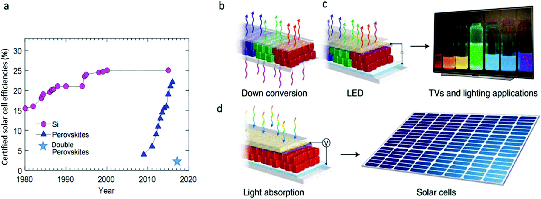 | ||
| Fig. 1 (a) Evolution of best researched solar cells’ efficiency comparing Si to lead halide perovskites (data adopted from National Renewable Energy Laboratory (NREL)). Recent published results for lead-free double perovskite cells Cs2AgBiBr6 state 2.2% efficiency.94 Owing to their high PLQYs, narrow PL FWHM, and tunability over the entire visible spectral range, lead halide perovskites nanocrystals can find applications in (b) PL down conversion, as used in LCD displays and lighting, (c) electroluminescent devices such as LEDs, and (d) solar cells. Reprinted with permission from Macmillan Publishers, Nature Materials,95 copyright (2018). | ||
The most concerning aspect of the practical applications of lead halide perovskites in large scale industries is the toxicity of lead. Replacing the lead in lead halide perovskites with other elements, while retaining the favorable optoelectronic properties, is not only of practical interest but also of fundamental importance. Understanding how cation transmutation in perovskites affects the resulting electronic structure and thermodynamic stability of the product is essential for future development of these materials.12
Nanocrystals are exciting testbeds for new materials since they are single structured domains where chemical transformations and finite size electronic effects can be studied. In the context of lead-free perovskites, nanocrystals can serve as a model system to study the composition band gap engineering. In nanocrystals, the exchange transformations are faster and require lower activation energies and are, therefore, useful for exploring various cationic transmutations. In addition, in quantum confined structures, the additional confinement energy may alter the electronic structure favoring non-trivial transitions. The nanocrystal can also affect the stability of materials. The crystallographic phases that are not stable at room temperature may become stable at the nanoscale due to the additional surface energy that comes with the increased surface to volume ratio.
Design rules for lead-free perovskites
When choosing elements that lead could be possibly replaced with, the basic chemical design rules can serve to narrow the search. To form structurally stable metal–halide octahedra and perovskites, the ionic radius and formal charge neutrality needs to be taken into consideration. The actual calculation of the compatibility of ions with the crystal structure is achieved using two indicators – the geometrical tolerance factor (Goldschmidt factor),13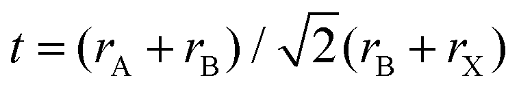 , and cation/anion radius ratio (octahedral factor),14μ = rB/rX, where rA, rB, and rX denote the ionic radius, which indicate the regions of interest for stable perovskite phases.13,15 To replace the toxic lead and still retain the three dimensional perovskite connectivity and the resulting favorable optoelectronic properties, a heterovalent substitution is implemented. Heuristically, the unit cell is doubled and a pair of Pb2+ ions is replaced by one M+ cation and one M3+ cation, as depicted in Fig. 2b. The resulting material is characterized by A2B+B3+X6 stoichiometry and crystallizes in the cubic space group Fm
![[3 with combining macron]](https://www.rsc.org/images/entities/char_0033_0304.gif) m.16 For double perovskites, there is a need to consider a specific octahedral factor for each type of octahedron. For the tolerance factor, a mere average of the B and B′ site ionic radii should be used. The theoretical conditions for a stable structure are μ > 0.41 and 0.75 < t < 1.0.17 As a design rule, the selection of ions based on their radii is of great importance. The octahedral factor limits the use of larger anions, for example, iodide in Cs2AgBiX6. In this specific case, the iodide ion does not form stable octahedra with small cations and therefore, the double perovskites structure can form only with Cl− and Br−. A similar phenomenon occurs with In and Sb double perovskite compositions where bromide anions are too big to form stable octahedra and only chloride compositions exist.
m.16 For double perovskites, there is a need to consider a specific octahedral factor for each type of octahedron. For the tolerance factor, a mere average of the B and B′ site ionic radii should be used. The theoretical conditions for a stable structure are μ > 0.41 and 0.75 < t < 1.0.17 As a design rule, the selection of ions based on their radii is of great importance. The octahedral factor limits the use of larger anions, for example, iodide in Cs2AgBiX6. In this specific case, the iodide ion does not form stable octahedra with small cations and therefore, the double perovskites structure can form only with Cl− and Br−. A similar phenomenon occurs with In and Sb double perovskite compositions where bromide anions are too big to form stable octahedra and only chloride compositions exist.
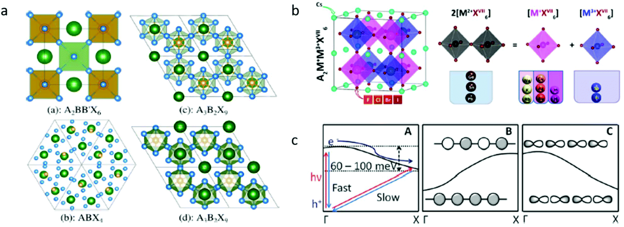 | ||
| Fig. 2 (a) Different perovskite-like structures. Structures (a), (c), and (d) are commonly referred to as double, 2-D layered, and 0-D dimer perovskite, respectively. Structures (c) and (d) are polymorphs. Reprinted (adapted) with permission from ref. 25. Copyright (2017) American Chemical Society. (b) Space of candidate A2M+M3+XVII6 perovskites for materials screening: left panel shows the adopted double-perovskite structure and the right panel shows the schematic idea of atomic transmutation. Reprinted (adapted) with permission from ref. 50. Copyright (2017) American Chemical Society. (c) (A) Proposed band diagram for tetragonal (CH3NH3) PbI3,96 (B) band structure for s-orbital derived bands, and (C) band structure for the p-orbital derived bands. Republished with permission of The Royal Society of Chemistry, from,42 copyright (2018). | ||
More complex theoretical studies were used for predicting the stability and properties of lead-free three-dimensional halide perovskites (ABX3).18,19 Filip et al. used ab initio calculations on hypothetical materials, in which lead is replaced with other divalent cations across the periodic table. The authors concluded that only Pb, Sn, and Ge based perovskites are stable materials that also show promising properties for optoelectronic applications.18 However, these simple geometric considerations do not always yield favorable results. For example, Travis et al.15 have shown that the Goldschmidt tolerance factor alone fails to predict the stability of many known inorganic iodide perovskites. Some of these exemplar materials require advance quantum mechanical corrections on top of the simple geometrical considerations.20
Moreover, replacing Pb2+ with Sn2+ or Ge2+ yields unstable materials, in which the divalent cations undergo rapid oxidation to tetravalent Sn4+ and Ge4+. This process, accompanied by a metal vacancy formation, changes the crystallographic structure and specifically, the connectivity of the metal halide octahedra. One example is the transition of CsSnI3, a 3D ABX3 perovskite structure, to Cs2SnI6, a vacancy-ordered material, in which the octahedra are isolated.21 In addition, properties such as defect tolerance may be reduced due to the loss of the outermost ns2 electrons.6 The lead-free divalent versions and the vacancy-ordered materials associated with them will not be discussed in this work and are beyond the scope of the double perovskite structures that we are focusing on herein.
Replacing lead with other cations that do not conform to the strict geometrical and oxidation state restrictions results in the formation of materials with stoichiometries other than the classical ABX3 and with lower symmetry space groups. For instance, A2BB′X6 (Fmm), ABX4 (R3c), A3B2X9 (Pm1), and the polymorph (P63/mmc) (see Fig. 2a). A common property of the lower symmetry group structure is the lower dimensional connectivity of the octahedra (e.g., zero dimensional and two-dimensional connectivity) vs. the extended three-dimensional connectivity in Fmm such as ABX3 and A2BB′X6. The lower dimensional connectivity in these materials typically leads to significant differences in the electronic properties such as higher energy band gaps22 and lower charge mobility.23 These properties are less appealing for applications that require high mobilities and efficient extraction of charge carriers such as in photovoltaic devices.
Combinatorial diversity via heterovalent substitution
The use of heterovalent substitutions for Pb2+ in the A2BB′X6 stoichiometry with its combinatorial degree of freedom expands the material family that can be explored in the search of lead-free, thermodynamically stable compounds. Some exemplary cations that can be used are Na+, K+, Rb+, Cu+, Ag+, Au+, In+, and Tl+ as monovalent cations and In3+, Sb3+, and Bi3+ as trivalent. Beyond stability, the electronic applications require materials that support efficient absorption and emission processes, which is usually found within materials that exhibit a direct band gap and strongly allowed lowest optical transitions.The directness of the band gap is determined by the crystal momenta of the valence band maximum and conduction band minimum. The difference in the orbital overlaps dictates the band behavior. While the s orbital derived bands will typically rise in energy from the center to edge of the Brillouin zone, the p orbital derived bands will decrease in energy (see Fig. 2c). In the scheme of a heterovalent substitution, by selecting the neighboring cations that exhibit the same orbital symmetry, one may effectively engineer the electronic structure and the nature of the resulting electronic transitions. The wide variety of available trivalent and monovalent cation combinations results in hundreds of possible new compounds of double perovskite materials. Computational studies have been conducted in order to narrow down the search to materials with desirable band gaps, charge carrier mobilities, and effective masses.24,25
We now bring a representative list of lead-free perovskites materials that have been synthesized in the bulk form and as nanocrystals. We show how the nanocrystals add to our understanding of stability and improve the optical properties such as the directness of the band gap.
Bulk and nanocrystals of Cs2AgBiX6
In 2016, multiple groups reported the successful synthesis of the double perovskites with Cs2AgBiX6 (X = Cl− or Br−) compositions.3,26–29 The resulting crystals exhibit a 3-dimensional network of corner-sharing alternating octahedra of [AgBr6] and [BiBr6], where the Cs+ cations are situated between the octahedra. The crystal structures match an ideal double perovskite, i.e., elpasolite or the K2NaAlF6 structure. The resulting Cs2AgBiBr6 material is considerably more heat and moisture resistant than most metal halide perovskites (see Fig. 3a–d).28,30,31 The theoretical and optical studies27,31–33 have shown that Cs2AgBiBr6 has an indirect band gap of ∼1.95 eV.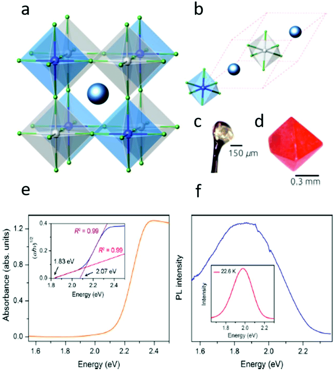 | ||
| Fig. 3 (a) Polyhedral model of the conventional unit cell. (b) Polyhedral model of the primitive unit cell of Cs2BiAgX6 (X = Cl, Br). The red dashed lines mark the primitive lattice vectors. The large dark blue spheres represent the Cs atoms. The small gray, blue, and green spheres are the Ag, Bi, and halogen atoms, respectively. (c) Single crystal of Cs2BiAgCl6. (d) Single crystal of Cs2BiAgBr6. Reprinted (adapted) with permission from ref. 27. Copyright (2016) American Chemical Society. (e) Absorbance spectrum of Cs2AgBiBr6 powder. Inset: Tauc plot showing the characteristics of an indirect band gap. (f) Steady-state room-temperature photoluminescence (PL) spectrum of a Cs2AgBiBr6 powdered sample upon 500 nm excitation. Inset: Low-temperature PL spectrum. Reprinted (adapted) with permission from ref. 32. Copyright (2016) American Chemical Society. | ||
The diffused absorption measurements show that the absorption region begins at 1.8 eV, followed by an immediate increase in the absorption near 2.1 eV (see Fig. 3e). Assuming an indirect allowed transition, the Tauc plot of the data is shown in the inset of Fig. 3e.
At room temperature, Cs2AgBiBr6 displays a weak PL centered at 1.87 eV (Fig. 3f). The PL at low temperature (23 K) is observed to be more intense and blue-shifted, centered at 1.98 eV. The increase in the intensity indicates a significant reduction in the non-radiative processes, whose origin is still not completely understood.
The organic–inorganic perovskite MA2AgBiBr6 (MA being CH3NH3+ methylammonium) can be synthesized. The optical transition in this material is also of indirect nature as expected.54 The hybrid double perovskite has a low band gap of 2.02 eV and is stable in air and moisture.
The iodide version of this material, MA2AgBiI6, was also demonstrated.34 It has a lower band gap of 1.96 eV, high-stability in ambient environment, and good electron transport performance. These studies have ignited interest in this new family of materials, both as practical materials for photovoltaic applications and as model systems for exploring the composition band gap tunability in new, benign perovskites.
Nanocrystals of the Cs2AgBiX6 double perovskites where independently reported by Creutz et al.,35 Zhou et al.,33 and Bekenstein et al.36 The synthetic methods that these studies used are very similar to those used in the lead halide system. Two methods were demonstrated: the hot injection method, in which Cs-oleate or trimethylsiloqsane-halide was injected into a hot flask containing the precursor salts, oleic acid, and oleylamine as ligands and an organic solvent, and the re-precipitation method, in which the salt precursors are dissolved in polar solvents and then dropped into an immiscible solvent containing the ligands.
The XRD analysis reveals that the nanocrystals are of the cubic structure with a Fmm space group and lattice spacing of 11.2 Å, similar to the structure that was published for the bulk material but with the typical Debye–Scherrer broadening. The resulting nanocrystals are highly crystalline with a typical cube shape and lengths of 8 nm and 10–20% size distribution, as can be seen in the transmission electron microscopic (TEM) studies in Fig. 4a and b.
 | ||
| Fig. 4 (a) High-resolution transmission electron microscopic (HRTEM) image of Cs2AgBiBr6 nanocrystals depicting the atomic lattice fringes and the faceted cubic shape of the crystals. The scale bar is 8 nm. (b) Low-resolution transmission electron microscopic (LRTEM) image of the same sample. The scale bar is 100 nm. (c) Ultraviolet (UV)/Vis absorption of dilute Cs2AgBiBr6 (red) and Cs2AgBiCl6 (blue) nanocrystal suspensions demonstrating the characteristic peaks at 430 and 365 nm, respectively. Inset shows a suspension of Cs2AgBiBr6 nanocrystals, with distinct yellow color different from the orange-red bulk material. Reprinted (adapted) with permission from ref. 36. Copyright (2018) American Chemical Society. (d)–(f) Single-crystal X-ray structures of the (001) layered double perovskites: (d) (BA)4AgBiBr8 (BA = CH3(CH2)3NH3+), (f) (BA)2CsAgBiBr7, and the 3D double perovskite (g) Cs2AgBiBr6.32 Insets show the Ag coordination sphere with select bond distances in angstroms. In the inset for B, t denotes a terminal bromide and b denotes a bridging bromide. Orange, white, turquoise, brown, blue, and gray spheres represent Bi, Ag, Cs, Br, N, and C atoms, respectively. H and disordered atoms omitted for clarity. (g), (h): Band structures corresponding to the 100 K experimental structures of (g) (BA)2CsAgBiBr7 and (h) (BA)4AgBiBr8. Note that the band structures are shown in duplicate, where the Ag (left panel) and Bi (right panel) states that compose the bands are represented by colored dots. Red arrows show the lowest-energy transitions. Reprinted (adapted) with permission from ref. 89. Copyright (2018) American Chemical Society. | ||
The most intriguing aspects of these nanocrystals are their optical properties. Historically, the contribution of quantum size effects may improve the absorption and emission from nanocrystals. To the naked eye, the Cs2AgBiBr6 nanocrystal suspension presents a distinct yellow color and is optically different from the orange-red color of the bulk material (see inset, Fig. 4c). The dilute solutions of Cs2AgBiBr6 nanocrystals have a typical absorption spectrum featuring a sharp absorption peak positioned at ∼430 nm and a long absorption tail at the longer wavelengths, suggesting an indirect transition that is consistent with the reported bulk properties. A similar functional form with a sharp peak is observed for the Cl compositions, with the peak positioned at 365 nm, as demonstrated in Fig. 4c. The striking difference in the appearance of the bulk and nanocrystalline material, and the existence of this sharp peak suggest an origin of quantum size effect in these features. Creutz et al. have reported shifts of the absorption features to lower energies for larger nanocrystals and concluded that these size-dependent properties are indicative of quantum confinement and hence, of delocalized charge carriers with large Bohr radii. It is worth noting that the bulk band gap value of Cs2AgBiBr6 is 2 eV, while in the nanocrystals the main absorption peak is centered at 2.88 eV, which is blue-shifted by more than 1 eV from the band edge. This means that if indeed this absorption feature originates from a quantum confined exciton, it is expected to be strongly dependent on the conditions of the experiment such as the size of crystals and dielectric environment confining the exciton.
In our own studies, we saw something different. We have conducted a size series experiment, in which both the size and dielectric environment of the nanocrystals were changed. However, the resulting position of the absorption peak in our studies did not shift significantly. This result leads us to conclude that the 430 nm peak in the Cs2AgBiBr6 system is a very localized transition. One such likely transition is the metal-centered s–p transition, similar to those of isolated metal halide molecular complexes containing filled s2 orbitals, which were spectroscopically studied by Oldenburg and Vogler.37
While the current Cs2AgBiBr6 colloidal nanocrystals seem not to present strong quantum confinement size effects, other hybrid organic–inorganic materials with different stoichiometries crystallize into two-dimensional structures. These experiments shed light on the limits within which the quantum confinement effects play a role in the double perovskites. Recently, the quantum confinement effects in Cs2AgBiBr6 were demonstrated by synthesizing two lower dimensional derivatives: a monolayer material with composition of (BA)4AgBiBr8 (BA = CH3(CH2)3NH3+) and a bilayer material (BA)2CsAgBiBr7 (Fig. 4d–f). Conner et al. have been able to show that by reducing the dimensionality of the inorganic Cs2AgBiBr6 layers of the material, significant structural and electronic differences emerge.
According to DFT calculations, Cs2AgBiBr6 undergoes an indirect-to-direct band gap transition in the monolayer material.
Although this transition is driven mainly by dimensional quantum confinement effects, research show that structural effects can also emphasize the reduced dimensionality transition. The Cs2AgBiBr6 monolayers and bilayers are both structurally heavily distorted predominantly at the Ag site. In particular, the Ag–Br octahedra present a tetragonal distortion with short chemical bonds between Ag and the axial terminal bromides (Ag–Brax = 2.6 Å) and long bonds between Ag and the bridging equatorial bromides Ag–Breq = 3 Å (see Fig. 4g and h). In the bilayer material, the Ag atoms protrude from either side of the inorganic sheets, sitting 0.4 Å out of the plane defined by the equatorial bridging bromides, and form a shorter bond with the axial terminal Br (2.6 Å) and a longer bond with the axial bridging Br (3 Å) (see Fig. 4g and h inset).
It is the mixing between the Ag and Bi frontier orbitals in the valence band and the conduction band that has been identified as the source of the indirect band gap in Cs2AgBiBr6.28,38 Due to the above structural distortion, such hybridization is prevented in the monolayers of Cs2AgBiBr6, which in turn exhibit a single metal orbital character at the band edges.
This transition, from an indirect band gap in the 3D material to a direct band gap in the 2D material, is reminiscent of the effects of exfoliation of the transition metal dichalcogenides.39,40 These accompanying structural distortions further separate the lowest-energy direct transition in the monolayers and indirect transition in the bilayer and bulk Cs2AgBiBr6.
Finally, one has to take both structural distortions and electronic modifications when considering the properties of these monolayer materials.
Compositional band gap engineering towards a direct transition
After the selection of desired compositions, the ability to alloy and dope one material into another is a powerful tool for manipulating and controlling the electronic properties. In general, the exchange of a significant number of atoms in a material, which result in a detectable structural change, is termed alloying. On the other hand, doping is the exchange of only a few atoms per nanocrystals up to a few percent with no significant effect on the overall structure.In Cs2AgBiBr6 double perovskite, the computed electronic structure is composed of a conduction band minimum that has Ag s, Bi p, and Br p character at the L point28 and a valence band maximum of Ag d, Bi s, and Br p character at the X point, which leads to an indirect band gap. It is the Bi s states at the top of the valence band that interact with the directional Ag d states along the [100] direction. This interaction shifts the valence band to the X point and leads to an indirect band gap, as was computationally demonstrated in Cs2AgBiCl6 by Volonakis.41
In standard semiconductors, it is difficult to independently tune the valence and conduction band since the bonding and anti-bonding states are paired. However, in the double perovskite (A2BB′X6) structure, independent tunability is possible. Specifically, one B cation can be d10, establishing the valence band states, while the second B′ contains the s/p states that make up the conduction bands. By adjusting the electron filling of B′ from s0 to s2, it is then possible to decouple the two and adjust the lowest conduction band between s orbital derived and p orbital derived while leaving the rest of the band structure essentially intact.
Such an approach was taken by Volonakis et al.41 and later studied by others.25,42–44 Volonakis has reported the direct synthesis of Cs2InAgCl6 and has shown a direct band gap transition, explained by the lack of occupied In-s orbitals in the valence band maximum. Cs2InAgCl6 has a space group of Fmm, long carrier lifetimes (6 μs), and a direct band gap of ∼2 eV at room temperature. The compound is found to be photosensitive and switches reversibly from white to orange under ultraviolet illumination. The researchers also performed an empirical analysis based on Goldschmidt's rules for the thermodynamic stability of Cs2AgInX6 and its mixed halides. The resulting conclusion was that Cl and Br alloys Cs2AgIn(Cl1−xBrx)6 are also stable for x < 1.
Du et al.45 and Tran et al.42 have shown that it is possible to systematically control the band gap values in halide perovskites via trivalent metal alloying and adjustment of the character of the conduction band. Tran et al. demonstrated that by a gradual substitution of Sb with In in a solid solution experiment of Cs2AgSb1−xInxCl6, a direct vs. indirect transition was observed. In particular, Cs2AgSbxIn1−xCl6 shows indirect transition for x ≥ 0.4 and direct transition when x < 0.4. Effectively, increasing the Sb composition changed the character of the conduction band minimum from s-orbital derived to p-orbital-derived, turning the transition to an indirect one and reducing the band gap values by ∼0.4 eV (see Fig. 5a). In the case of a 100% Sb composition, the Cs2AgSbCl6 bulk perovskite is also stable and can be directly synthesized.42,46 This material crystallizes in the cubic Fmm space group and has shown to exhibit an indirect transition with band gap value of ∼3 eV.
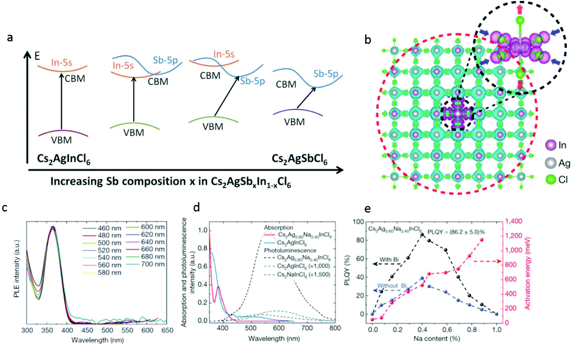 | ||
| Fig. 5 (a) Proposed band diagram for Cs2AgSbxIn1−xCl6 depicting a change in the character of the conduction band minimum (CBM) from s-orbital derived to p-orbital derived while having the valence band maximum (VBM). Primarily, the Ag-d states result in a transition from the direct to indirect band gap. Republished with permission of The Royal Society of Chemistry, from42 copyright (2018). (b) Self trapped excitons in Cs2AgInCl6. Cs atoms are omitted for clarity. The cyan and magenta isosurfaces represent the electron and hole orbital densities, respectively. The electron state (red dashed circle) is rather extended and the hole state (black dashed circle) is compact, which is consistent with the small (large) effective mass of the conduction (valence) band. The hole isosurface is obvious, whereas the electron isosurface is invisible owing to its small density. (c)–(e) Characterization of Cs2AgxNa1−xInCl6 with different Na content. All Cs2AgxNa1−xInCl6 samples were doped using a small amount (0.04%, atomic ratio to In) of Bi, and the compositions were determined from inductively coupled plasma atomic emission spectroscopy (ICP-OES) results. (c) Excitation spectra of photoluminescence measured at different wavelengths. (d) Optical absorption (solid lines) and photoluminescence (dashed lines) spectra of pure Cs2AgInCl6 and Cs2Ag0.60Na0.40InCl6. (e) Activation energy and PLQY of Cs2AgxNa1−xInCl6 powder versus Na content. The dashed lines are guides for the eye. Reprinted with permission from Macmillan Publishers, Nature,47 Copyright (2018). | ||
Now, we will return to discuss the direct band gap material Cs2AgInCl6. The main challenge with the electronic configuration of Cs2AgInCl6 is that the transitions close to the band edge are completely Laporte forbidden due to angular momentum conservation considerations.
One approach to overcome this challenge is to partially substitute the Ag with a cation that fits the geometrical constrains of the double-perovskite structure, namely, the Goldschmidt's tolerance and the geometrical octahedral factors but has a typically different electronic configuration than Ag.
Luo et al.47 have demonstrated that by alloying Na cations into Cs2AgInCl6, they could overcome the dark transition, which is dictated by the crystals’ inversion symmetry that forces a parity forbidden transition, resulting in a direct band gap. They have reported that their best Na doped samples with 0.04 percent bismuth doping reached an impressive ∼86% PLQY as opposed to <0.1% in the pristine Cs2AgInCl6. The light that is emitted from this system has a broad spectrum from 460 to 700 nm. This is further confirmed by the photoluminescence excitation spectra, which exhibit identical characteristics, signifying that the white emission originates from the relaxation of the same excited state (see Fig. 5c and d). The broadband and white emission is normally associated with self-trapped excitons that may exist in semiconductors with localized carriers and a soft lattice such as halide perovskites. These excitons arise from a Jahn–Teller distortion and specifically in our case of the AgCl6 octahedra (see Fig. 5b). Through DFT calculations, the researchers show that the Ag–Cl bonds are elongated by 0.08 Å in the axial direction but compressed by 0.2 Å in the equatorial plane. These excitons share the same orbital character as the free exciton, resulting in a parity-forbidden transition and low photoluminescence quantum yield in the native material. Here, the sodium doping comes into play and poses a dual effect. Firstly, it changes the orbital nature and symmetry of the wave function of the self-trapped exciton, effectively breaking the parity-forbidden transition. The second includes reduction of the electronic dimensionality of the semiconductor. This leads to an increase in the PL efficiency by three orders of magnitude compared to pure Cs2AgInCl6, as presented in Fig. 5e.
Hybrid organic–inorganic materials were also demonstrated. The synthesis of MA2AgInBr6 was reported by Tran et al.48 Despite the identical stoichiometry, (MA)2AgInBr6 does not form with a double perovskite structure due to a very large a/b cation ratio. Instead, (MA)2AgInBr6 crystallizes in the trigonal space group Pm1, which is essentially a 1D chain of face sharing, [AgBr6] [InBr6] alternating octahedra, and the MA molecules are positioned in the empty spaces between the chains.
Since many of the compounds discussed herein contain indium, it is worth noting that indium is multivalent and can take either the position of the monovalent or the trivalent cations as In(I) and In(III), respectively. Following this idea, Cs2InBiX6 and Cs2InSbX6 bulk perovskite crystals where theoretically investigated.17,49,50 According to the studies, these materials exhibit direct band gaps with small charge carrier effective masses. The main problem is that they suffer from an inherent instability to oxidation. Specifically, In(I) is unstable and will oxidize into thermodynamically stable In(III) based compounds.
Less explored compositions of double perovskites
The use of thallium (Tl) in double perovskite counters the common intuition since it is more toxic than lead that we wish to replace. Recent work by Slavney et al.51 demonstrated that surprising band gap engineering is possible with Tl substitution due to its multiple oxidation states Tl(III) and TI(I). It was shown that by alloying Cs2AgBiBr6 with Tl, in the regime of low Tl concentrations, Tl(III) appears to substitute for Bi(III). The optical spectra show that the band gap decreases by ∼0.6 eV at 10% of Tl doping. In another work, they have demonstrated that in the case of a total exchange of Bi(III) with Tl, one gets a full direct band gap transition, resulting in black crystals instead of yellow ones.51 In the concentrated Tl regime, the Tl/Ag site mixing occurs readily and the crystals change back their color to yellow. The nature of the optical transition in this underexplored family of alloys, namely, Cs2Ag1−xTl+Tl+3X6 is unclear and still remains to be studied.Other interesting perovskite compositions can be obtained with the use of sodium or potassium in the B site. The synthesis and properties of Cs2NaBiCl6 were studied during 197052 and recently by others.53–55 This perovskite is characterized by the Fmm space group and calculations predict that it has a large indirect band gap of above 3.0 eV.50
In 1982 and 1986, the synthesis of Fmm Cs2KBiCl6 was reported.3,56,57 This material has recently gained attention by the work of Zhao et al.,50 which calculated this material to have an indirect transition with robust thermodynamic stability. Wei et al.58 have shown that the organic version of this perovskite, MA2KBiCl6, is also stable. This later perovskite is interesting since it has a wide indirect band gap of ∼3 eV and shows strong similarities to the lead analogues (MA)PbCl3.
Currently, no nanocrystals of these compositions have been made and it remains for future studies to investigate if quantum confinement effects with potassium in the B site can induce an indirect-direct electronic transition. Further compositions including potassium in the B site include the use of rare-earth based double perovskites, which have been discovered many years ago. MA2KGdCl6 and MA2KYCl6 were synthesized by Deng et al.59 These hybrid perovskites adopt a rhombohedral structure with Rm symmetry at room temperature and transfer to the cubic phase on heating to around 162 °C for (MA)2KYCl6 and 102 °C for (MA)2KGdCl6. The relatively low temperature of this transition makes these materials interesting for studying relations between the structural and electronic transitions in double perovskites. We note in passing that (MA)2KGdCl6 is also predicted to exhibit low temperature magnetic ordering and it may be interesting in the context of investigations of the Rashba effect that was already observed in the lead-based perovskites.60
In general, all the aforementioned less-explored compositions were not made as nanocrystals. It is reasonable to assume that some of the synthetic pathways developed for halide double perovskites will benefit in the synthesis of nanocrystals from the above materials. In particular, it will be interesting to explore the properties of rare-earth double perovskites at the nanoscale. Recent observations61 of doping of Cs2AgInCl6 nanocrystals with erbium (Er+3) and ytterbium (Yb+3) show promise of a rich and interesting system that enables the wavelength tunability of lanthanide IR emissions.
Doping and alloying in double perovskite nanocrystals
At the nanoscale, doping or alloying processes commonly used for the tuning of electronic properties of bulk double perovskites may no longer be as effective.The introduction of impurity atoms into a nanocrystal that contains only hundreds to thousands of atoms is not trivial and in some material systems may pose a technical challenge due to the expulsion of impurities to the nanocrystal surface or by altering of the crystal structure.62,63
In addition, in strongly quantum confined systems, the dopants behave different than in bulk because their electronic wave functions are confined to a small volume. For instance, in n-type or p-type impurities, auto-ionization without thermal activation may occur. This happens since the carriers inside the nanocrystals must occupy a confined space. The confined states increase in energy with decreasing nanocrystal size. Below some critical radius, the confinement energy exceeds the Coulomb interaction between the ionized impurity and the carrier,64 and as a result the dopant will ionize and a carrier will occupy a nanocrystal state. This is very relevant when discussing doping and alloying of double perovskite nanocrystals.
The synthesis of double perovskite nanocrystals is at its infancy with only a few papers that report their synthesis and properties.33,35,36
However, it is apparent that many lessons learned from the lead-halide perovskite nanocrystals can also be implemented in the lead-free synthetic process. One such example is the use of metal carboxylate precursors and acyl-halides for controlling the reaction conditions and the resulting sizes of the nanocrystals. Locardi et al.44 have reported a synthetic method that enables good control over the size distribution. Essentially, benzoyl chloride serves as the halide source and is injected into a metal carboxylate precursor (Cs-oleate, Ag–In-acetates), mixed with ligands and a solvent (diphenylether). This technique allows for the fine adjustment of the ratio of the cation precursors, which react only upon injection of the chloride precursor, thus resulting in size controlled Cs2AgInCl6 double perovskite nanocrystals. However, controlling the size of these nanocrystals by itself does not significantly change their electronic properties, indicating low or no quantum confinement in these nanocrystals, similar to the aforementioned Cs2AgBiX6 compositions. Here, however doping plays an important role.
Doping with Mn(II) ions in the semiconducting nanocrystals is a known method to tune the electrical properties. Such doping of Cs2AgInCl6 was recently demonstrated by Nandha et al.65 and Locardi et al.44 In particular, the researchers have reported a typical broad orange PL emission (λem = 620 nm) with PLQYs toping at 16 ± 4% at 1.5% Mn doping. It is interesting to note that when higher feed concentrations of Mn(II) were used in the synthesis, no further inclusion of dopants was observed. Through photoluminescence excitation spectroscopy, Locardi et al. show that the orange emission originates on excitation of the nanocrystals above 350 nm, at energies comparable to that of the optical gap, which essentially means that the energy absorbed at the Cs2AgInCl6 band edge is transferred to the Mn2+ impurities and reemitted, similar to the mechanisms previously reported for Mn-doped semiconductors.
In nanocrystals, the large surface to volume ratio enables facile exchange chemistries, thus improving the efficiency of the solid solution and the alloying processes.
Yang et al.66 have synthesized and characterized Cs2AgInCl6 nanocrystals (see Fig. 6a–e). Then, they implemented the same kind of Bi–In trivalent metal substitution as described in bulk. In nanocrystals, in addition to the ability to engineer an indirect – direct transition through indium substitution, the researchers showed that the direct-band gap nanocrystals exhibit greater absorption cross-section and higher PL quantum efficiency (PLQE) compared with those observed for the indirect band gap Cs2AgBiCl6 nanocrystals. The increase was non-linear in nature with a sudden increase in PLQE between Cs2AgInxBi1−xCl6 (x = 0, 0.25, 0.5) and those recorded for Cs2AgInxBi1−xCl6 (x = 0.75, 0.9) compositions, as shown in Fig. 6f. The highest recorded PLQE of Cs2AgIn0.9Bi0.1Cl6 nanocrystals is 36.6%. This value is greater than five times of 6.7% that was observed for indirect-band gap of Cs2AgBiCl6 nanocrystals, and is comparable to those measured in CsPbCl3 nanocrystals.8,67–71 It is worth noting the similarities between this report and the work mentioned earlier by Luo (conducted on bulk material),47 in which sodium was used to break the inversion symmetry of the crystals and effectively increase the PLQY. Here, the maximum emission is also achieved at a mixed composition, in which 90% of indium is being alloyed by 10% Bi, effectively relieving the selection rule constrain that is imposed by the inversion symmetry. In this current work, there is no reference to self-trapped excitons and their role in the emission process. It will be interesting to explore the effects of sodium alloying in Cs2AgInCl6 nanocrystals, compare it to the work of Luo et al. in bulk microcrystalline material and to the claims regarding the role sodium plays in the confinement of the self-trapped excitons.
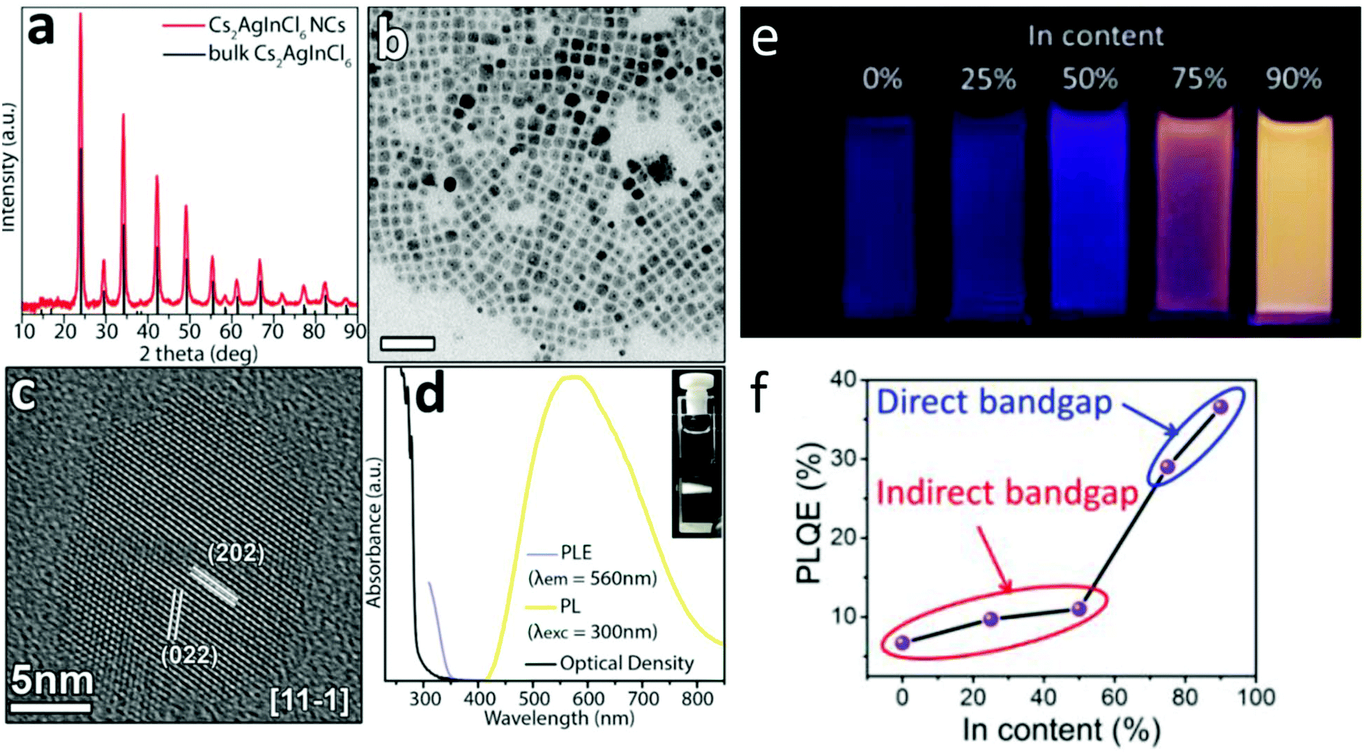 | ||
| Fig. 6 (a) XRD pattern of the nanocrystal product with the corresponding reflections of bulk Cs2AgInCl6 (ICSD number 257115). (b) Lower resolution TEM and the dark spots observed in the individual nanocubes are metallic Ag formed by the electron beam during the observation. The scale bar is 50 nm. (c) HRTEM micrographs of Cs2AgInCl6 nanocrystals. (d) Absorption, PL, and PL excitation (PLE) spectra of a Cs2AgInCl6 nanocrystal dispersion in hexane, and a photo of the PL emission from the cuvette under Xe lamp excitation at 300 nm (inset PL image of Cs2AgInxBi1−xCl6 (x = 0 and 0.9) nanocrystals under a UV light of 365 nm). This is an unofficial adaptation of an article that appeared in an ACS publication.44 (e) PL image of Cs2AgInxBi1–xCl6 under UV light of 365 nm. (f) PLQE value of Cs2AgInxBi1−xCl6 (x = 0, 0.25, 0.5, 0.75, and 0.9) nanocrystals capped with 8% oleic acid. Reprinted (adapted) with permission from ref. 97. Copyright (2018) American Chemical Society. | ||
Exploring the stability in nanocrystals of lead-free perovskites
One of the ongoing challenges with the perovskite family of materials is the stability towards degradation. The ionic nature of the halide perovskite makes them an order of magnitude more sensitive to humidity than Cd based semiconductors.72 Oxidation may pose another challenge and lead to significant material transformations such as in the case of tin based materials.21Nanocrystals, with their increased surface area to volume ratio, have been shown to stabilize thermodynamically unstable phases.73 For instance, the perovskite cubic α-CsPbI3 black phase, which is unstable at room temperature and in ambient conditions in the bulk material. This phase is metastable when it is made in the form of nanocrystals and can survive up to a few days in solution. With surface treatment and ligand exchange, the CsPbI3 nanocrystalline black phase has been shown to be stable enough and even support stable working solar cells, thus enabling the use of enhanced stability at the nanoscale in working devices.8,74
The fabrication of crystalline thin films is particularly challenging in the case of lead-free perovskites, particularly when using the standard solution processing methods. For instance, it is reported that the precursor's solubility may limit the crystalline domain size when fabricating solar cells.75 This can be solved by the use of colloidal nanocrystals to fabricate lead-free nanocrystal assemblies that are later sintered or fused to form thin films. This has been previously achieved with other more standard types of nanocrystals such as CdSe and PbS.76,77 The analogues of lead halide perovskite nanocrystals have proven to be very efficient when used as precursors for sintered thin films due to their soft nature and dynamic ligand binding.74,78 From the synthetic similarities between the lead-based and lead-free perovskites, it seems reasonable to assume that the lead-free nanocrystals will also serve as efficient sintering precursors for the fabrication of thin films.
Nanocrystals can also stabilize unstable double perovskite phases. Cs2AgBiI6 is not stable in bulk phase and was not experimentally demonstrated, despite being highlighted by computational studies as having a photovoltaic relevant band gap. The actual calculations for Cs2AgBiI6 predict that the enthalpy for spontaneous degradation is negative, and therefore the material will decompose to CsAg2I3 and Cs3Bi2I9.
Through anion exchange chemistry, Creutz et al. have shown that it is possible to access Cs2AgBiI6 at the nanoscale. They have used trimethylsilyl iodide (TMSI) to induce an exchange reaction of the bromides to iodides. We note in passing that direct colloidal synthesis of Cs2AgBiI6 is unsuccessful, emphasizing the advantages of using nanocrystals and facile exchange chemistries to obtain materials that are impossible to achieve in any other way.
Outlook for potential applications
This review will not be complete without a perspective outlook of the potential uses of the materials we have discussed. While photovoltaic applications are the first to come to mind due to the successes of the hybrid lead halide perovskites and similar structure of 3D corner sharing connected octahedra, other applications such as light emitting diodes, lasers, and photodetectors are also reasonable when considering the recent high PLQY observations from some of these materials. The presence of heavy elements in the double perovskites opens the possibility of using double perovskites as efficient X-ray detectors and scintillators.79 Herein, we bring examples where lead-free double perovskites have been implemented into devices of the above categories.Lead-free double perovskite-based solar cells have been recently fabricated.3,4,80–82 The preliminary reports of these devices are twofold. On the one hand, lead halide double perovskites can serve as decent solar absorbers that are characterized by good stability and band gap tunability due to diverse chemical compositions. However, on the other hand, poor film quality still challenges the fabrication of devices and more work has to be done in order to bring photo conversion values to compete with their lead-based counterparts. P type Cs2AgInCl6 and Cs2AgBiCl6 are good candidates for targeted photovoltaic or visible light/radiation detection applications.83 Also, the absorption coefficients of Cs2AgInX6 (X = Br or Cl), especially that of Cs2AgInBr6, are deteriorated negligibly by strain, making them potential materials for further applications in photovoltaics and flexible optoelectronics.84,85
For example, Cs2AgBiBr6 films were synthesized and fabricated into photovoltaic working devices.86,87 Currently, these device show relatively low power conversion efficiencies (PCE) close to 2.5% and an open circuit voltage (Voc) exceeding one volt. However, this early example shows the potential of double perovskites as lead-free absorber materials.
Recent advances in increasing the PLQY of Cs2AgInCl6via successful Na alloying have demonstrated warm-white light emission of 86 ± 5 percent PLQY. The researchers have also demonstrated a working prototype performing over 1000 hours.47
This white light-emitting double perovskite composition, which demonstrates outstanding stability and low manufacturing cost, may hold promise for better and affordable solid-state lighting in the future. While these properties were demonstrated in micro sized crystals, it may be that a nanoscale crystallite may both improve the emission properties and enable better incorporation into polymers to form flexible and highly luminescence composite films. We believe that such materials may be of interest and use in future display and lighting applications, however, deeper study is needed in order to realize their full potential and enable better control of the emitted spectrum.
High Z elements that typically compose double halide perovskites significantly increase the cross-section for the interaction of high energy radiations such as X-ray and gamma rays with the crystal. Researchers have demonstrated the use of lead-free double perovskites for sensitive detection of X-ray photons by direct photon-to-current conversion.88 The detector that was demonstrated was of high sensitivity and significantly lower production cost in comparison to traditional detectors. This observation opens opportunities for detection and scintillation of high energy into visible light that may prove important for future detectors.
The diversity of compounds that can be implemented via a double perovskite structure and their electronic band-gap values that span the visible and near UV spectrum make us believe that the aforementioned examples are not the last.
For future reference, we have listed the representative theoretical and experimental band gap values along with the type of electronic transitions of many lead-free double perovskite compounds (Table 1, Fig. 7). Lead-free double perovskites that have been grown successfully into nanocrystals are summarized in Table 2.
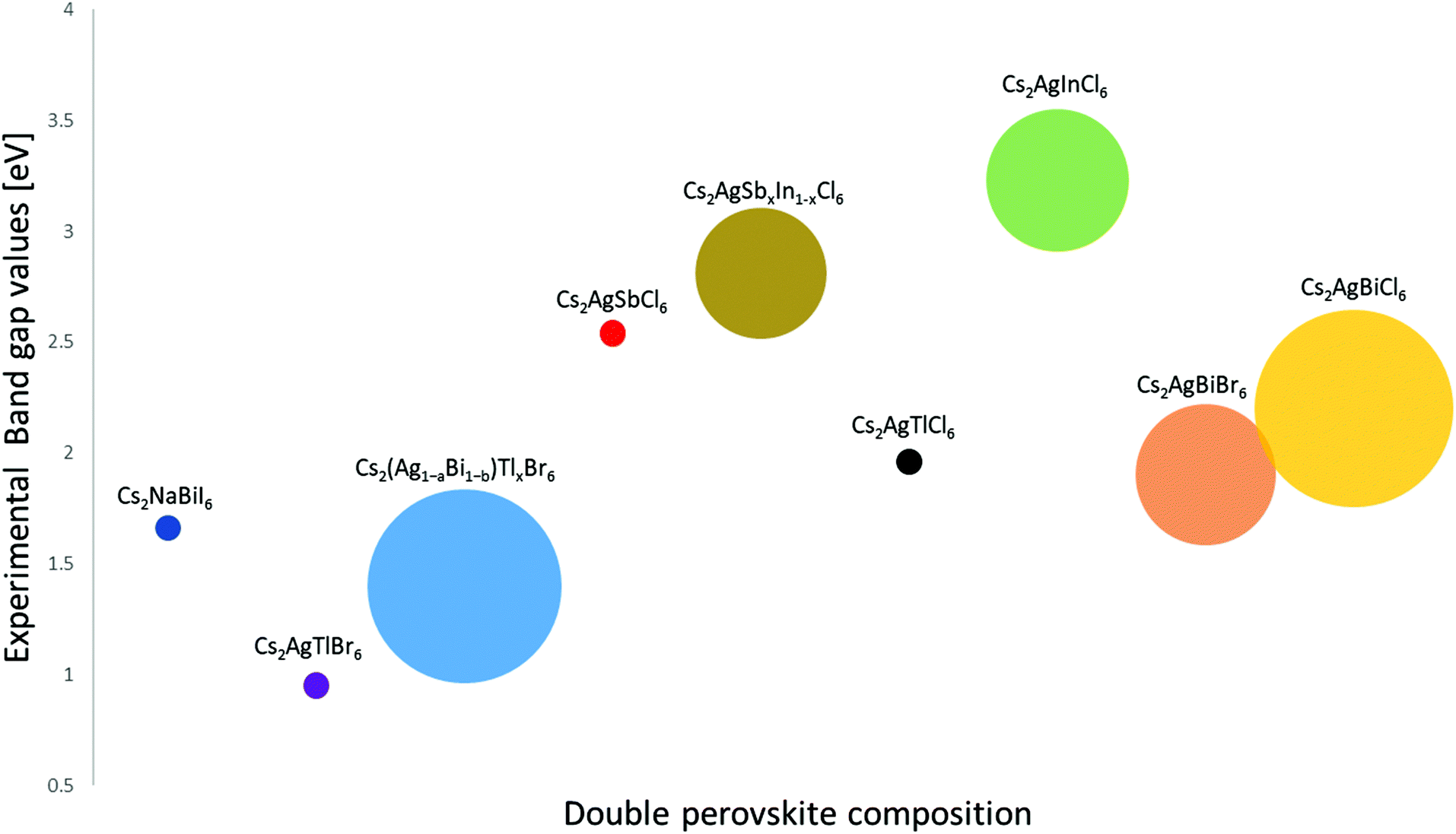 | ||
| Fig. 7 Representative group of the synthesized lead-free inorganic double perovskites compounds and their experimental band-gap values. The size of the circle represents the reported range of the band-gap values. The full data set and reference to the appropriate literature is listed in Table 1. | ||
| Material | Bulk band gap structure and characteristics | ||
|---|---|---|---|
| Optical transition | Theoretical value [eV] | Experimental value [eV] | |
| Cs2AgBiBr6 | Indirect3,20,27–29,31,32,50,82,89,90 | Values greatly vary, as low as 1.09 (2.4) for X = Br (X = Cl) and as high as 2.21 (2.62) for X = Br (X=Cl), depending on the calculation method: 1.09–2.21 (X = Br)20,27,28,50,90,82 | 1.9–2.19 (X = Br) |
| Cs2AgBiCl6 | 2.4–2.62 (X = Cl)27,28,50,90 | 2.2–2.77 (X = Cl)27,28,31,32,90 | |
| MA2AgBiBr6 | Indirect34,91 | ∼2 (X = Br)34 | 2.02 (X = Br)34 |
| MA2AgBiI6 | 1.63 (X = I)91 | 1.96 (X = I)91 | |
| Cs2AgInBr6 | Direct according to the theoretical work92 | 1.5 for Cs2AgInBr6, 2.5 for Rb2AgInCl6, 1.46 for Rb2AgInBr6, 1.36 for Rb2CuInCl6, 0.63 for Rb2CuInBr6![[thin space (1/6-em)]](https://www.rsc.org/images/entities/char_2009.gif) 92 92 |
|
| Rb2AgInCl6 | |||
| Rb2AgInBr6 | |||
| Rb2CuInCl6 | |||
| Rb2CuInBr6 | |||
| Cs2AgInCl6 | Direct25,41–43,47,92 | Values greatly vary, as low as 0.93 and as high as 3.23, depending on the calculation method: 0.93–3.3325,41,43,47 | 3.23–3.5341–43,47 |
| Cs2AgSbCl6 | Indirect42,46,50 | 1.40, 2.3546 depending on the calculation method. 2.4050 | 2.5442 |
| Cs2AgSbxIn1−xCl6 | Indirect for (x ≥ 0.4) and direct for (x < 0.4)42 | 2.81 (x = 0.5), 2.92 (x = 0.4), 3.06 (x = 0.2)42 | |
| Cs2InBiX6 | Direct according to theoretical work,17,49,50 | 0.91, 0.88 (X = Cl), 0.33 (X = Br), 0.21 (X = I), 2.22 (X = F)17,49,50 | |
| MA2InBiBr6 (Cs0.5MA0.5)2InBiBr6 *(FA0.5MA0.5)2InBiBr6 *FA = CH(NH2)2 formamidinium. | Direct according to theoretical work17 | 2.0 for MA2InBiBr6. 1.7 for (Cs0.5MA0.5)2InBiBr6. 1.9 for (FA0.5MA0.5)2InBiBr6.17 | |
| Cs2InSbX6 | Direct according to the theoretical work49,50 | 1.02, 0.98 (X = Cl), 0.41 (X = Br), 0.17 (X = I), 2.37 (X = F)49,50 | |
| (MA)2TlBiBr6 | Direct90 | 1.04, 0.5290 depending on the calculation method. | 2.1690 |
| Cs2AgTlCl6, Cs2AgTlBr6 | Direct51 | 1.87, 2.17 (X = Cl), 0.63, 0.82 (X = Br)51 depending on the calculation method. | 1.96 (X = Cl), 0.95 (X = Br)51 |
| Cs2(Ag1−aBi1−b)TlxBr6 0.003 < x = a + b < 0.075 | Direct for low Tl concentrations, indirect for high Tl concentrations according to theoretical work51,90 | 1.09 when assuming indirect, 1.3 when assuming direct.90 | For x = 0.5: 1.95 when assuming direct, 1.85 when assuming indirect. For x = 0.75: 1.6 when assuming direct, 1.4 when assuming indirect.90 |
| Cs2KBiCl656,57 | Indirect according to theoretical work50 | 4.1850 | |
| MA2KBiCl6 | Indirect3,58 | 3.0258 | 3.0458 |
| MA2KGdCl6 | Direct according to theoretical work59 | 4.9159 | |
| MA2KYCl6 | Direct according to theoretical work59 | 5.0459 | |
| Cs2NaBiCl652–55 | Indirect according to theoretical work50 | 3.9650 | |
| Cs2NaBiI6 | Indirect50,93 | 2.4250 | 1.6693 |
| Material | Nanocrystals band gap structure and characteristics | ||
|---|---|---|---|
| Optical transition | Experimental value [eV] | Quantum confinement effect? | |
| Cs2AgBiBr6, Cs2AgBiCl6, Cs2AgBiI6 | Indirect33,35,36 | 1.97–2.52 (X = Br),33,35,36 2.9 (X = Cl),35 1.75 (X = I)35 | Observed35/not observed36 |
| Cs2AgInxBi1−xCl6 | Direct for (x = 0.75 and 0.9) and indirect for (x = 0, 0.25, and 0.5)66 | 2.35–2.82 indirect, 3.04–3.23 direct66 | |
| Cs2AgInCl6 | Direct66 | 4.0666, 4.3844 | Observed44 |
Concluding remarks
Lead-free double perovskites, their different composition, and associated properties have been discussed. It is apparent that relative to the vast compositions synthesized in bulk, only a few lead-free double perovskites were synthesized as nanocrystals. At the nanoscale, these materials have already shown quantum size effects but only when confined to monolayers. The added surface energy in nanocrystals has shown to increase stability in metastable phases. For example, Cs2AgBiI6 cannot be made in bulk but was shown to be a stable nanocrystal. Due to their quaternary nature, the combinatorial compositions available in double perovskites enable flexible band gap tunability and electronic structure engineering. These preliminary indications are an open invitation for fellow researches to further explore these materials at the nanoscale. The current challenges in the field are many such as improving the optoelectronic properties, which include enhancing the absorption cross-section and photoluminescence quantum yield of these materials. For devices, the improvement of conversion efficiencies currently focuses much of the engineering interest. Nanocrystals can be important participants in these studies, especially when material composition plays an important role. This is due to the facile ion exchange reactions at the nanoscale. This marks double perovskite nanocrystals as interesting model systems to keep in mind when exploring, developing, and engineering design rules for next generation optoelectronic materials.Conflicts of interest
There are no conflicts to declare.Acknowledgements
Y. B. and S. K. thanks the Hellen Diller quantum center and the Nancy and Stephen Grand Technion energy program, for their generous support of our new group. Y. B. thanks the Irwin and Bethea Green and Detroit chapter career advancement chair. Y. B. acknowledges support from the Energy and Water Resources Ministry of Israel as part of their postdoctoral fellowship program in leading universities abroad, support that has laid the foundations to this work. We thank R. Shechter for proof reading the manuscript.References
- A. Kojima, K. Teshima, Y. Shirai and T. Miyasaka, J. Am. Chem. Soc., 2009, 131, 6050–6051 CrossRef CAS PubMed.
- M. A. Green and A. Ho-Baillie, ACS Energy Lett., 2017, 2, 822–830 CrossRef CAS.
- F. Giustino and H. J. Snaith, ACS Energy Lett., 2016, 1, 1233–1240 CrossRef CAS.
- Q. Xu, D. Yang, J. Lv, Y.-Y. Sun and L. Zhang, Small Methods, 2018, 2, 1700316 CrossRef.
- S. D. Stranks, G. E. Eperon, G. Grancini, C. Menelaou, M. J. P. Alcocer, T. Leijtens, L. M. Herz, A. Petrozza and H. J. Snaith, Science, 2013, 342, 341–344 CrossRef CAS PubMed.
- R. E. Brandt, V. Stevanović, D. S. Ginley and T. Buonassisi, MRS Commun., 2015, 5, 265–275 CrossRef CAS.
- K. Miyata, T. L. Atallah and X.-Y. Zhu, Sci. Adv., 2017, 3, 1701469 CrossRef PubMed.
- L. Protesescu, S. Yakunin, M. I. Bodnarchuk, F. Krieg, R. Caputo, C. H. Hendon, R. X. Yang, A. Walsh and M. V. Kovalenko, Nano Lett., 2015, 15, 3692–3696 CrossRef CAS PubMed.
- Y. Bekenstein, B. A. Koscher, S. W. Eaton, P. Yang and A. P. Alivisatos, J. Am. Chem. Soc., 2015, 137, 16008–16011 CrossRef CAS PubMed.
- B. A. Koscher, J. K. Swabeck, N. D. Bronstein and A. P. Alivisatos, J. Am. Chem. Soc., 2017, 139, 6566–6569 CrossRef CAS PubMed.
- Q. A. Akkerman, G. Rainò, M. V. Kovalenko and L. Manna, Nat. Mater., 2018, 17, 394–405 CrossRef CAS PubMed.
- D. A. Egger, A. Bera, D. Cahen, G. Hodes, T. Kirchartz, L. Kronik, R. Lovrincic, A. M. Rappe, D. R. Reichman and O. Yaffe, Adv. Mater., 2018, 30, 1800691 CrossRef PubMed.
- V. M. Goldschmidt, Naturwissenschaften, 1926, 14, 477–485 CrossRef CAS.
- L. Pauling, J. Am. Chem. Soc., 1929, 51, 1010–1026 CrossRef CAS.
- W. Travis, E. N. K. Glover, H. Bronstein, D. O. Scanlon and R. G. Palgrave, Chem. Sci., 2016, 7, 4548–4556 RSC.
- M. R. Filip, G. E. Eperon, H. J. Snaith and F. Giustino, Nat. Commun., 2014, 5, 5757 CrossRef CAS PubMed.
- G. Volonakis, A. A. Haghighirad, H. J. Snaith and F. Giustino, J. Phys. Chem. Lett., 2017, 8, 3917–3924 CrossRef CAS PubMed.
- M. R. Filip and F. Giustino, J. Phys. Chem. C, 2016, 120, 166–173 CrossRef CAS.
- S. Körbel, M. A. L. Marques and S. Botti, J. Mater. Chem. C, 2016, 4, 3157–3167 RSC.
- Z. Xiao, W. Meng, J. Wang and Y. Yan, ChemSusChem, 2016, 9, 2628–2633 CrossRef CAS PubMed.
- X. Qiu, B. Cao, S. Yuan, X. Chen, Z. Qiu, Y. Jiang, Q. Ye, H. Wang, H. Zeng, J. Liu and M. G. Kanatzidis, Sol. Energy Mater. Sol. Cells, 2017, 159, 227–234 CrossRef CAS.
- A. J. Lehner, D. H. Fabini, H. A. Evans, C.-A. Hébert, S. R. Smock, J. Hu, H. Wang, J. W. Zwanziger, M. L. Chabinyc and R. Seshadri, Chem. Mater., 2015, 27, 7137–7148 CrossRef CAS.
- B. Ghosh, B. Wu, H. K. Mulmudi, C. Guet, K. Weber, T. C. Sum, S. Mhaisalkar and N. Mathews, ACS Appl. Mater. Interfaces, 2018, 10, 35000–35007 CrossRef PubMed.
- S. Chakraborty, W. Xie, N. Mathews, M. Sherburne, R. Ahuja, M. Asta and S. G. Mhaisalkar, ACS Energy Lett., 2017, 2, 837–845 CrossRef CAS.
- A. Jain, O. Voznyy and E. H. Sargent, J. Phys. Chem. C, 2017, 121, 7183–7187 CrossRef CAS.
- A. H. Slavney, T. Hu, A. M. Lindenberg and H. I. Karunadasa, J. Am. Chem. Soc., 2016, 138, 2138–2141 CrossRef CAS PubMed.
- M. R. Filip, S. Hillman, A. A. Haghighirad, H. J. Snaith and F. Giustino, J. Phys. Chem. Lett., 2016, 7, 2579–2585 CrossRef CAS PubMed.
- E. T. McClure, M. R. Ball, W. Windl and P. M. Woodward, Chem. Mater., 2016, 28, 1348–1354 CrossRef CAS.
- W. Ning, X.-G. Zhao, J. Klarbring, S. Bai, F. Ji, F. Wang, S. I. Simak, Y. Tao, X.-M. Ren, L. Zhang, W. Huang, I. A. Abrikosov and F. Gao, Adv. Funct. Mater., 2019, 1807375 CrossRef.
- A. H. Slavney, T. Hu, A. M. Lindenberg and H. I. Karunadasa, J. Am. Chem. Soc., 2016, 138, 2138–2141 CrossRef CAS PubMed.
- G. Volonakis, M. R. Filip, A. A. Haghighirad, N. Sakai, B. Wenger, H. J. Snaith and F. Giustino, J. Phys. Chem. Lett., 2016, 7, 1254–1259 CrossRef CAS PubMed.
- A. H. Slavney, T. Hu, A. M. Lindenberg and H. I. Karunadasa, J. Am. Chem. Soc., 2016, 138, 2138–2141 CrossRef CAS PubMed.
- L. Zhou, Y.-F. Xu, B.-X. Chen, D.-B. Kuang and C.-Y. Su, Small, 2018, 14, 1703762 CrossRef.
- F. Wei, Z. Deng, S. Sun, F. Zhang, D. M. Evans, G. Kieslich, S. Tominaka, M. A. Carpenter, J. Zhang, P. D. Bristowe and A. K. Cheetham, Chem. Mater., 2017, 29, 1089–1094 CrossRef CAS.
- S. E. Creutz, E. N. Crites, M. C. De Siena and D. R. Gamelin, Nano Lett., 2018, 18, 1118–1123 CrossRef CAS PubMed.
- Y. Bekenstein, J. C. Dahl, J. Huang, W. T. Osowiecki, J. K. Swabeck, E. M. Chan, P. Yang and A. P. Alivisatos, Nano Lett., 2018, 18, 3502–3508 CrossRef CAS PubMed.
- K. Oldenburg and A. Vogler, Z. Naturforsch., B: J. Chem. Sci., 1993, 48, 1519–1523 CAS.
- C. N. Savory, A. Walsh and D. O. Scanlon, ACS Energy Lett., 2016, 1, 949–955 CrossRef CAS PubMed.
- A. Splendiani, L. Sun, Y. Zhang, T. Li, J. Kim, C.-Y. Chim, G. Galli and F. Wang, Nano Lett., 2010, 10, 1271–1275 CrossRef CAS PubMed.
- K. F. Mak, C. Lee, J. Hone, J. Shan and T. F. Heinz, Phys. Rev. Lett., 2010, 105, 136805 CrossRef PubMed.
- G. Volonakis, A. A. Haghighirad, R. L. Milot, W. H. Sio, M. R. Filip, B. Wenger, M. B. Johnston, L. M. Herz, H. J. Snaith and F. Giustino, J. Phys. Chem. Lett., 2017, 8, 772–778 CrossRef CAS PubMed.
- T. T. Tran, J. R. Panella, J. R. Chamorro, J. R. Morey and T. M. McQueen, Mater. Horiz., 2017, 4, 688–693 RSC.
- J. Zhou, Z. Xia, M. S. Molokeev, X. Zhang, D. Peng and Q. Liu, J. Mater. Chem. A, 2017, 5, 15031–15037 RSC.
- F. Locardi, M. Cirignano, D. Baranov, Z. Dang, M. Prato, F. Drago, M. Ferretti, V. Pinchetti, M. Fanciulli, S. Brovelli, L. De Trizio and L. Manna, J. Am. Chem. Soc., 2018, 140, 12989–12995 CrossRef CAS PubMed.
- K. Du, W. Meng, X. Wang, Y. Yan and D. B. Mitzi, Angew. Chem., Int. Ed., 2017, 56, 8158–8162 CrossRef CAS PubMed.
- J. Zhou, X. Rong, M. S. Molokeev, X. Zhang and Z. Xia, J. Mater. Chem. A, 2018, 6, 2346–2352 RSC.
- J. Luo, X. Wang, S. Li, J. Liu, Y. Guo, G. Niu, L. Yao, Y. Fu, L. Gao, Q. Dong, C. Zhao, M. Leng, F. Ma, W. Liang, L. Wang, S. Jin, J. Han, L. Zhang, J. Etheridge, J. Wang, Y. Yan, E. H. Sargent and J. Tang, Nature, 2018, 563, 541–545 CrossRef CAS PubMed.
- T. T. Tran, M. A. Quintero, K. E. Arpino, Z. A. Kelly, J. R. Panella, X. Wang and T. M. McQueen, CrystEngComm, 2018, 20, 5929–5934 RSC.
- Z. Xiao, K.-Z. Du, W. Meng, J. Wang, D. B. Mitzi and Y. Yan, J. Am. Chem. Soc., 2017, 139, 6054–6057 CrossRef CAS PubMed.
- X.-G. Zhao, J.-H. Yang, Y. Fu, D. Yang, Q. Xu, L. Yu, S.-H. Wei and L. Zhang, J. Am. Chem. Soc., 2017, 139, 2630–2638 CrossRef CAS PubMed.
- A. H. Slavney, L. Leppert, A. Saldivar Valdes, D. Bartesaghi, T. J. Savenije, J. B. Neaton and H. I. Karunadasa, Angew. Chem., Int. Ed., 2018, 57, 12765–12770 CrossRef CAS PubMed.
- L. R. Morss, M. Siegal, L. Stenger and N. Edelstein, Inorg. Chem., 1970, 9, 1771–1775 CrossRef CAS.
- F. Pelle, B. Blanzat and B. Chevalier, Solid State Commun., 1984, 49, 1089–1093 CrossRef CAS.
- W. M. A. Smit, G. J. Dirksen and D. J. Stufkens, J. Phys. Chem. Solids, 1990, 51, 189–196 CrossRef CAS.
- W. Urland, Chem. Phys. Lett., 1981, 83, 116–119 CrossRef CAS.
- P. Barbier, M. Drache, G. Mairesse and J. Ravez, J. Solid State Chem., 1982, 42, 130–135 CrossRef CAS.
- F. Benachenhou, G. Mairesse, G. Nowogrocki and D. Thomas, J. Solid State Chem., 1986, 65, 13–26 CrossRef CAS.
- F. Wei, Z. Deng, S. Sun, F. Xie, G. Kieslich, D. M. Evans, M. A. Carpenter, P. D. Bristowe and A. K. Cheetham, Mater. Horiz., 2016, 3, 328–332 RSC.
- Z. Deng, F. Wei, F. Brivio, Y. Wu, S. Sun, P. D. Bristowe and A. K. Cheetham, J. Phys. Chem. Lett., 2017, 8, 5015–5020 CrossRef CAS PubMed.
- M. Isarov, L. Z. Tan, M. I. Bodnarchuk, M. V. Kovalenko, A. M. Rappe and E. Lifshitz, Nano Lett., 2017, 17, 5020–5026 CrossRef CAS PubMed.
- W. Lee, S. Hong and S. Kim, J. Phys. Chem. C, 2019, 2665–2672 CrossRef CAS.
- G. M. Dalpian and J. R. Chelikowsky, Phys. Rev. Lett., 2006, 96, 226802 CrossRef PubMed.
- T.-L. Chan, M. L. Tiago, E. Kaxiras and J. R. Chelikowsky, Nano Lett., 2008, 8, 596–600 CrossRef CAS PubMed.
- A. I. Ekimov, I. A. Kudryavtsev, M. G. Ivanov and A. L. Efros, J. Lumin., 1990, 46, 83–95 CrossRef CAS.
- K. N. Nandha and A. Nag, Chem. Commun., 2018, 54, 5205–5208 RSC.
- B. Yang, X. Mao, F. Hong, W. Meng, Y. Tang, X. Xia, S. Yang, W. Deng and K. Han, J. Am. Chem. Soc., 2018, 140, 17001–17006 CrossRef CAS PubMed.
- G. Nedelcu, L. Protesescu, S. Yakunin, M. I. Bodnarchuk, M. J. Grotevent and M. V. Kovalenko, Nano Lett., 2015, 15, 5635–5640 CrossRef CAS PubMed.
- Y.-S. Park, S. Guo, N. S. Makarov and V. I. Klimov, ACS Nano, 2015, 9, 10386–10393 CrossRef CAS PubMed.
- J. Song, J. Li, X. Li, L. Xu, Y. Dong and H. Zeng, Adv. Mater., 2015, 27, 7162–7167 CrossRef CAS PubMed.
- Y. Wang, X. Li, J. Song, L. Xiao, H. Zeng and H. Sun, Adv. Mater., 2015, 27, 7101–7108 CrossRef CAS PubMed.
- M. Imran, V. Caligiuri, M. Wang, L. Goldoni, M. Prato, R. Krahne, L. De Trizio and L. Manna, J. Am. Chem. Soc., 2018, 140, 2656–2664 CrossRef CAS PubMed.
- B. Hailegnaw, S. Kirmayer, E. Edri, G. Hodes and D. Cahen, J. Phys. Chem. Lett., 2015, 6, 1543–1547 CrossRef CAS PubMed.
- S. H. Tolbert and A. P. Alivisatos, Science, 1994, 265, 373–376 CrossRef CAS PubMed.
- A. Swarnkar, A. R. Marshall, E. M. Sanehira, B. D. Chernomordik, D. T. Moore, J. A. Christians, T. Chakrabarti and J. M. Luther, Science, 2016, 354, 92–95 CrossRef CAS PubMed.
- C. Wu, Q. Zhang, Y. Liu, W. Luo, X. Guo, Z. Huang, H. Ting, W. Sun, X. Zhong, S. Wei, S. Wang, Z. Chen and L. Xiao, Adv. Sci., 2018, 5, 1700759 CrossRef PubMed.
- J.-H. Choi, A. T. Fafarman, S. J. Oh, D.-K. Ko, D. K. Kim, B. T. Diroll, S. Muramoto, J. G. Gillen, C. B. Murray and C. R. Kagan, Nano Lett., 2012, 12, 2631–2638 CrossRef CAS PubMed.
- M. Law, J. M. Luther, Q. Song, B. K. Hughes, C. L. Perkins and A. J. Nozik, J. Am. Chem. Soc., 2008, 130, 5974–5985 CrossRef CAS PubMed.
- Q. A. Akkerman, M. Gandini, F. Di Stasio, P. Rastogi, F. Palazon, G. Bertoni, J. M. Ball, M. Prato, A. Petrozza and L. Manna, Nat. Energy, 2017, 2, 16194 CrossRef CAS.
- X.-G. Zhao, D. Yang, J.-C. Ren, Y. Sun, Z. Xiao and L. Zhang, Joule, 2018, 2, 1662–1673 CrossRef CAS.
- M.-G. Ju, M. Chen, Y. Zhou, J. Dai, L. Ma, N. P. Padture and X. C. Zeng, Joule, 2018, 2, 1231–1241 CrossRef CAS.
- F. Igbari, R. Wang, Z.-K. Wang, X.-J. Ma, Q. Wang, K.-L. Wang, Y. Zhang, L.-S. Liao and Y. Yang, Nano Lett., 2019, 2066–2073 CrossRef CAS PubMed.
- J. Kangsabanik, V. Sugathan, A. Yadav, A. Yella and A. Alam, Phys. Rev. Mater., 2018, 2, 55401 CrossRef CAS.
- T. Li, X. Zhao, D. Yang, M.-H. Du and L. Zhang, Phys. Rev. Appl., 2018, 10, 41001 CrossRef CAS.
- Z. Zhang, J. Su, J. Hou, Z. Lin, Z. Hu, J. Chang, J. Zhang and Y. Hao, J. Phys. Chem. Lett., 2019, 10, 1120–1125 CrossRef CAS PubMed.
- H. Cho, S.-H. Jeong, M.-H. Park, Y.-H. Kim, C. Wolf, C.-L. Lee, J. H. Heo, A. Sadhanala, N. Myoung, S. Yoo, S. H. Im, R. H. Friend and T.-W. Lee, Science, 2015, 350, 1222–1225 CrossRef CAS PubMed.
- E. Greul, M. L. Petrus, A. Binek, P. Docampo and T. Bein, J. Mater. Chem. A, 2017, 5, 19972–19981 RSC.
- W. Ning, F. Wang, B. Wu, J. Lu, Z. Yan, X. Liu, Y. Tao, J.-M. Liu, W. Huang, M. Fahlman, L. Hultman, T. C. Sum and F. Gao, Adv. Mater., 2018, 30, 1706246 CrossRef PubMed.
- W. Pan, H. Wu, J. Luo, Z. Deng, C. Ge, C. Chen, X. Jiang, W.-J. Yin, G. Niu, L. Zhu, L. Yin, Y. Zhou, Q. Xie, X. Ke, M. Sui and J. Tang, Nat. Photonics, 2017, 11, 726–732 CrossRef CAS.
- B. A. Connor, L. Leppert, M. D. Smith, J. B. Neaton and H. I. Karunadasa, J. Am. Chem. Soc., 2018, 140, 5235–5240 CrossRef CAS PubMed.
- A. H. Slavney, L. Leppert, D. Bartesaghi, A. Gold-Parker, M. F. Toney, T. J. Savenije, J. B. Neaton and H. I. Karunadasa, J. Am. Chem. Soc., 2017, 139, 5015–5018 CrossRef CAS PubMed.
- W. D. Pengfei Cheng, T. Wu, Y. Li, L. Jiang and K. Han, New J. Chem., 2017, 41, 9598 RSC.
- X.-G. Zhao, D. Yang, Y. Sun, T. Li, L. Zhang, L. Yu and A. Zunger, J. Am. Chem. Soc., 2017, 139, 6718–6725 CrossRef CAS PubMed.
- C. Zhang, L. Gao, S. Teo, Z. Guo, Z. Xu, S. Zhao and T. Ma, Sustainable Energy Fuels, 2018, 2, 2419–2428 RSC.
- W. Gao, C. Ran, J. Xi, B. Jiao, W. Zhang, M. Wu, X. Hou and Z. Wu, ChemPhysChem, 2018, 19, 1696–1700 CrossRef CAS PubMed.
- Q. A. Akkerman, G. Rainò, M. V. Kovalenko and L. Manna, Nat. Mater., 2018, 17, 394–405 CrossRef CAS PubMed.
- E. M. Hutter, M. C. Gélvez-Rueda, A. Osherov, V. Bulović, F. C. Grozema, S. D. Stranks and T. J. Savenije, Nat. Mater., 2017, 16, 115–120 CrossRef CAS PubMed.
- B. Yang, X. Mao, F. Hong, W. Meng, Y. Tang, X. Xia, S. Yang, W. Deng and K. Han, J. Am. Chem. Soc., 2018, 140(49), 17001–17006 CrossRef CAS PubMed.
| This journal is © The Royal Society of Chemistry 2019 |