
 Open Access Article
 This Open Access Article is licensed under a Creative Commons Attribution-Non Commercial 3.0 Unported Licence
Gate-tuned conductance of graphene-ribbon junctions with nanoscale width variations†
Young-Jun
Yu‡
 *a,
Jong-Ho
Choe‡
b,
Jong Yun
Kim
a,
Oh Hun
Gwon
a,
Hong Kyw
Choi
c,
Jin Sik
Choi
d,
Jin Hong
Kim
d,
Jin-Soo
Kim
b,
Jin Tae
Kim
c,
Jun-Hwan
Shin
c and
Young Kyu
Choi
c
*a,
Jong-Ho
Choe‡
b,
Jong Yun
Kim
a,
Oh Hun
Gwon
a,
Hong Kyw
Choi
c,
Jin Sik
Choi
d,
Jin Hong
Kim
d,
Jin-Soo
Kim
b,
Jin Tae
Kim
c,
Jun-Hwan
Shin
c and
Young Kyu
Choi
c
aDepartment of Physics, Chungnam National University, 99 Daehak-ro, Yuseong-gu, Daejeon, 34134, Korea. E-mail: yjyu@cnu.ac.kr
bDepartment of Physics, Korea University, Anam-dong 5, Seonbuk-gu, Seoul, 02841, Korea
cElectronics and Telecommunications Research Institute (ETRI), 218 Gajeong-ro, Yuseong-gu, Daejeon, 34129, Korea
dDepartment of Physics, Konkuk University, 120 Neungdong-ro, Gwangjin-gu, Seoul 05029, Korea
First published on 4th March 2019
Abstract
To utilize graphene as interconnection electrodes in high-density nanoelectronic structures, the electrical stability of graphene should be guaranteed under nanometer-scale deviations. Graphene-ribbon (GR) junctions with accessible dimensions (i.e., sub-micrometer widths) are used in diverse interconnection electrode applications and should be characterized properly if they are to be applied in high-density nanoelectronics. Analyzing the effects of nanoscale GR width variations on the conductance of the entire graphene electrode is necessary for their proper characterization. Here, we diagnose the conductance and thermal effect of graphene electrode junctions constructed from GRs of various widths and directions under gate-tuned voltages. On applying partial gate voltages, we identify the effect of local potential variance on the entire graphene electrode junction. As a result, we were able to perceive precise and minute conductance variations for the entire graphene electrode, arising mainly from different sub-micrometer-scale widths of the GRs, which could not be distinguished using conventional global gating methods.
Introduction
Two-dimensional (2D) crystals such as graphene or transition metal dichalcogenides (TMDCs) have been favored for atomically thin electronic applications demanding high charge-carrier mobility, large on–off ratios, and the capability of overcoming short-channel effects.1–12 In particular, graphene is suitable for use in interconnections and waveguide electrodes between atomically thin electrical and optical devices in flexible, transparent, high-performance circuits.10–19 To achieve high performance from 2D semiconductor field-effect transistors (FETs), we should overcome the tremendous contact resistance of the 2D semiconductor channel with conventional metal electrodes, which degrades the carrier-transport performance. Graphene has been employed as an electrode for decreasing contact resistance, because the Fermi levels of the 2D crystal channel and the graphene electrode are close.8,10–15 Moreover, when graphene with atomic thickness and high conductivity is used as an optical waveguide electrode on flexible and transparent devices, the conductivity of the graphene waveguide reflects the shape of the guided optical wave and its efficiency.16–19 Thus, the conductivity of graphene electrodes depends on variations in dimensions such as width and is an important factor for nanometer-scale applications in electrical and optical devices. There have been several reports on the theoretical and experimental characterization of variations in the conductance of individual graphene ribbons (GRs) without width variations, on the application of an electrically global gating condition.20–26 However, these studies have focused mainly on ultra-narrow (∼ a few nanometers wide) graphene nanoribbon structures with quantized conductance variations ascribed to localized state effects. For the application of graphene in interconnections of 2D crystal FET arrays, the adaptable dimensions (∼ sub-micrometer width) of the GRs used in the electrodes should be confirmed with predictable conductance variations. Therefore, direct measurement of the partially nanoscale width-difference-dependent conductance variation of the entire GR junction electrode is necessary. A scanning probe microscope (SPM) can be used to perform nanoscale graphene surface characterization.27,28 In particular, upon applying an electric gate on desired nanoscale GR areas via a conductive SPM probe, we can investigate the direct effect of individual GR widths on the entire GR junction electrode conductance, which is not revealed by applying a global gating avenue.In this work, to diagnose the effect of sub-micrometer variations in GRs on conductance, we demonstrate junction structures composed of GRs with various widths. We investigate the conductance variation as a function of width by applying electrical biases and gate voltages. As a result, while conductance variations generally expected for GR junctions with a sub-micrometer width range, on the application of a global gating voltage through the SiO2 substrate, are from 40% to 69%, we could detect precise and minute conductance variations (ranging from 0.3% to 3.0%) over the GR junction, which were contributed by individual GRs on applying a partial gating voltage with a conductive SPM probe.
Results and discussion
To investigate width-dependent conductance variations in graphene electrodes, we employed GR junctions with different widths (Fig. 1(a)). The GR junctions were prepared using polymethyl methacrylate (PMMA) e-beam resist as an etch mask in an oxygen plasma etching process, which removed the unprotected graphene (for more details see the Experimental section and ESI, Fig. S1 and S2†). The widths of GR ranged from 100 to 500 nm, targeting sub-micrometer scale interconnection electrodes. For the interconnection applications of graphene electrodes in high-density device arrays, there should be sub-micrometer scale variations in the width and direction. Therefore, we employed various GR junction devices with widths ranging from ∼95 to ∼470 nm, lengths ranging from 4.0 to 5.5 μm, and directions differing between types (I), (II), and (III) (Fig. 1(a)). The GR junctions were terminated with a gradually widening graphene area in contact with Cr/Au electrodes. On applying a global back-gate voltage VBG (Fig. 1(b)), the observed transport characteristics of the type (I) GR junction (Fig. 1(a)) exhibited slightly p-doped behavior with a charge-neutral position VCNP = 18.5 V (Fig. 1(c)). Here, the carrier density (![[n with combining macron]](https://www.rsc.org/images/entities/i_char_006e_0304.gif) = 2.61 × 1012 cm−2) induced in graphene by the charged impurities was extracted by correlating the currents obtained through experiments and simulations of the entire GR junction under the biased voltage VDS (for more details of the calculation of , see the Experimental section and ESI†). We also calculated similar = 2.64 × 1012 cm−2 and 2.48 × 1012 cm−2 for type (II) and (III) GRs with VCNP = 12.5 V and 13.7 V, respectively (see ESI, Fig. S3 and S4†). As a result, the initial Fermi level (E0) in the proposed schematic diagram in the inset of Fig. 1(c) could be calculated as E0 = ħνF(π)1/2 = 188 meV for the graphene in type (I). Similarly, E0 for types (II) and (III) was estimated as 190 meV and 184 meV, respectively. Here, ħ and νF = 1 × 10⁶ m s−1 are the Planck's constant and Fermi velocity of graphene, respectively. As the transport curve in Fig. 1(c) was measured by applying VBG through 280 nm thick SiO2 dielectric layers, was the averaged initial carrier density of the entire GR junction structure. Therefore, we can employ this transport curve as a reference for the conductance variation by applying a gate voltage. A more precise inspection, such as that using SPM, can be employed for confirming the conductance variation for the entire GR junction, caused by individual GRs with different widths, on the application of a gate electric field (Fig. 1(b)).
= 2.61 × 1012 cm−2) induced in graphene by the charged impurities was extracted by correlating the currents obtained through experiments and simulations of the entire GR junction under the biased voltage VDS (for more details of the calculation of , see the Experimental section and ESI†). We also calculated similar = 2.64 × 1012 cm−2 and 2.48 × 1012 cm−2 for type (II) and (III) GRs with VCNP = 12.5 V and 13.7 V, respectively (see ESI, Fig. S3 and S4†). As a result, the initial Fermi level (E0) in the proposed schematic diagram in the inset of Fig. 1(c) could be calculated as E0 = ħνF(π)1/2 = 188 meV for the graphene in type (I). Similarly, E0 for types (II) and (III) was estimated as 190 meV and 184 meV, respectively. Here, ħ and νF = 1 × 10⁶ m s−1 are the Planck's constant and Fermi velocity of graphene, respectively. As the transport curve in Fig. 1(c) was measured by applying VBG through 280 nm thick SiO2 dielectric layers, was the averaged initial carrier density of the entire GR junction structure. Therefore, we can employ this transport curve as a reference for the conductance variation by applying a gate voltage. A more precise inspection, such as that using SPM, can be employed for confirming the conductance variation for the entire GR junction, caused by individual GRs with different widths, on the application of a gate electric field (Fig. 1(b)).
 | ||
| Fig. 1 (a) GR junction structures. Type (I): Straight GR junctions with widths of ∼470, 290, and 200 nm. Type (II): a 45° path-changed GR junction with ∼133 nm wide sides and a ∼95 nm wide center. Type (III): a 90° path-changed GR junction with ∼170 nm wide sides and a ∼170 nm wide center. The lengths of the GRs in each type of sample are approximately 1 μm. (b) Schematic diagram of a GR FET on SiO2/Si and its conductance, SGM, and SThM measurements. (c) Current variation of the GR junction of (a) type (I) as a function of global back-gate voltage (VBG). Here, there is a level marker (dashed line and arrow) for checking the charge neutral position (VCNP). Inset: Current variation of the GR junction as a function of bias voltage (VDS) and schematic diagram of graphene energy potential exhibiting slightly p-doped behavior with E0. | ||
Fig. 2(a) shows an electric field microscopy (EFM, VEFM) image of a GR junction with VDS = 0.5 V. Here, the represented GR junction is type (I), as shown in Fig. 1(a), constructed with 470, 290, and 200 nm widths and ∼1 μm length for the individual GRs. In the EFM image exhibiting the conductance of the graphene area (Fig. 2(a)), the electrical isolation of the GR junctions from the initially exfoliated graphene flakes corresponding to the AFM image of type (I) (Fig. 1(a)) is guaranteed and a gradually sloping electric potential is observed between the ends of the GR junction marked with A and B (Fig. 2(a)), owing to the application of a bias voltage VDS = 0.5 V. Here, we can observe that the variation of the potential is the largest in the widest part of the GR due to a larger electric field, exhibiting greater slope for GR with 470 nm width than for GR with 290 and 200 nm widths (see ESI, Fig. S5†). Although the width-dependent Joule self-heating temperature difference (ΔT = 5 to 15 K for 470 to 200 nm width with VDS = 2 V) in the GR junction was not large, the ΔT variation agreed well with the conductance of the GR junctions, as a function of width and VBG (Fig. 2(b) and (c), respectively; see also ESI, Fig. S3 and S4†). This indicates that the width-dependent conductance of GR is dominant among the electrical and thermal properties of a GR junction.
 | ||
| Fig. 2 (a) EFM image of applying VDS = 0.5 V for the type (I) GR junction shown in Fig. 1. Here, the points marked A and B in the color scale bar correspond to ΔVEFM ∼ 0.5 V for positions marked by A and B on the EFM image of the GR junction and the dashed box indicates the same area of (b) SThM and (Fig. 3) SGM images. (b) Temperature distribution images of a Joule self-heated type (I) GR junction for applied VDS = 2 V and VBG = 0–25 V. (c) Temperature variation at GR widths of 200 nm (red dots), 290 nm (purple dots) and 470 nm (blue dots), as a function of VBG. Temperature values were extracted from (b) SThM images as a function of VBG. The current variation (dashed line) of the GR junction as a function of VBG is the same as that in Fig. 1(c). | ||
For the direct measurement of the gate voltage contribution to the individual conductance of the GR in the junction structure constructed with different widths or directions, we employed scanning gate microscopy (SGM) (Fig. 1(b)).27–31 By applying a partial gate voltage to each different strip width area, the conductance variation of the GR junction contributed by the ribbon structure could be investigated, as shown in Fig. 3(a–c). From the SGM measurements, by applying a partial gate voltage VT = ±8 V using a conductive SGM probe at a constant height of 100 nm, we deduce the Fermi level of the GR junction tuned in the hole-doping region to be E0 ± ΔET = ħνF[( ± Δn)π]1/2 = 169–206 meV by roughly estimating Δn = CAir·VT/e = ±0.5 × 1012 cm−2, as proposed in the schematic diagrams in the inset of Fig. 3(a) and (b), where Δn and CAir are the charge-carrier density induced by applying a gate voltage (VT or VBG) and capacitance of air with 100 nm distance between the SGM probe and GR, respectively. Based on this charge-carrier density variation of graphene, induced by VT, the SGM images of the GR junctions (Fig. 3(a) and (b)) exhibited a width dependency leading to conductance variations around (I − I0)/I0 = 0.29% to 0.94% for widths between 470 and 200 nm (see Fig. 3(c)). Here, I and I0 are the current values of the entire GR junction, with and without a gating voltage applied over individual GR areas, respectively. The (I − I0)/I0 values used in this work were absolute values for comparing the variations as a function of the width and gate voltage.
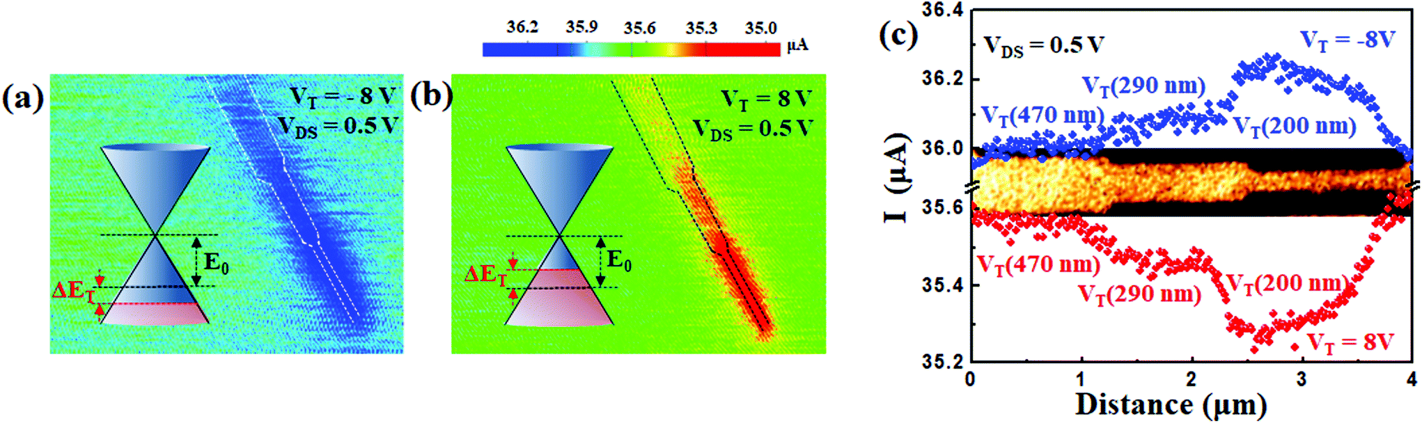 | ||
| Fig. 3 (a) and (b) SGM images for VT = ±8 V for the type (I) GR junction biased by VDS = 0.5 V. Inset: Schematic diagrams of graphene energy potential exhibiting doping change with E0 ± ΔET. (c) Conductance profiles of (a) and (b) SGM images along the GR junction. Here, the VT (470 nm), VT (290 nm), and VT (200 nm) marks indicate the partial gating by VT on individual GRs with widths of ∼470 nm, ∼290 nm, and ∼200 nm, respectively. The cropped EFM image of Fig. 2(a) is shown at the center of the plots for correlating current variations with GR features. | ||
GR junction structures of various widths and paths have been fabricated and characterized (Fig. 1(a) and Fig. S2†), and we confirmed that the width variation was significantly more dominant than the path change for our specimens. Namely, although type (II) and (III) GR junctions with a ribbon of 1 μm length had path changes of 45° and 90°, respectively, variations were not observed in the transport characteristics owing to a short mean free path in graphene on SiO2 (see ESI, Fig. S3 and S4†).13,32–35 Note that, upon employing the ballistic conditions for suspended graphene or graphene on a hexagonal boron nitride (hBN) substrate, which can suppress charge impurities and improve carrier mobility above 500![[thin space (1/6-em)]](https://www.rsc.org/images/entities/char_2009.gif) 000 cm2 V−1 s−1, the mean free path can be increased to micrometer scales.32–35 However, our GR junctions on SiO2 possessing a few hundred nanometers width and few micrometers length, exhibited a carrier mobility of approximately several thousand cm2 V−1 s−1 (i.e., 2000 to 4000 cm2 V−1 s−1 for 2.61 × 1012 cm−2 of the hole carrier density region for our specimens) because of the electron–hole puddles created by the SiO2 substrate. Therefore, the mean free path should have been smaller than 1 μm. Conventional dielectric substrates such as SiO2 lead to short mean free paths and do not allow path-dependent transport variations in graphene. On the other hand, because we observed substantial width-dependent conductance variations (see also ESI, Fig. S3 and S4†), we focused our analysis on the width-dependent conductance variations of GR junctions on the application of gate voltages.
000 cm2 V−1 s−1, the mean free path can be increased to micrometer scales.32–35 However, our GR junctions on SiO2 possessing a few hundred nanometers width and few micrometers length, exhibited a carrier mobility of approximately several thousand cm2 V−1 s−1 (i.e., 2000 to 4000 cm2 V−1 s−1 for 2.61 × 1012 cm−2 of the hole carrier density region for our specimens) because of the electron–hole puddles created by the SiO2 substrate. Therefore, the mean free path should have been smaller than 1 μm. Conventional dielectric substrates such as SiO2 lead to short mean free paths and do not allow path-dependent transport variations in graphene. On the other hand, because we observed substantial width-dependent conductance variations (see also ESI, Fig. S3 and S4†), we focused our analysis on the width-dependent conductance variations of GR junctions on the application of gate voltages.
For comparing the electric-field effect on the GR/SiO2 structure by gating either VT or VBG (Fig. 4(a)), we numerically calculated electric potential distributions, reflecting notably different electric potential distributions between the GR and the dielectric areas under gating of either VT or VBG in Fig. 4(b) or (c), respectively (for details of the calculations, see the Experimental section and ESI, Fig. S6–S8†). Applying VT = 8 V via the SGM probe at a distance of 100 nm from the GR surface created an electric potential at the exact desired position of the GR, with almost invariant electric potential of the SiO2 substrate (see Fig. 4(b)). The global gating voltage VBG = 8 V applied through the 280 nm thick SiO2 substrate caused a doping change in the entire GR in both SiO2 and air (see Fig. 4(c)). As a result, the global gating voltage VBG produced a carrier-density change over the entire GR area, as shown by the large carrier density Δn ∼ 1.54 × 1012 cm−2 at the center of the GR (x = 0) (Fig. 4(d–f)). On the other hand, the application of VT by the SGM probe induced a carrier density change in graphene, which could be exactly ascribed to the SGM probe position (x = y = 0 nm), as well as its rapid suppression on increasing |y| (red line in Fig. 4(e)), while Δn by VBG was invariant along the length direction (blue line in Fig. 4(e)). Furthermore, we found that Δn under both VBG and VT was enhanced at the edge of the GR owing to the geometry, the state of the graphene edge, and the electric field strength.26 The Δn for VT was slightly smaller than that for VBG, albeit the SGM probe was applied at the GR edge (see also ESI, Fig. S7†). Here, although the GR with 100 nm width is representatively exhibited in Fig. 4, we calculated and employed Δn for all width conditions from 500 nm to 100 nm, with the aim of extracting the conductivities of the GR junctions (see ESI, Fig. S8†).
 | ||
| Fig. 4 (a) Schematic diagram of SGM measurements of GR and the marked vertical cross-section area between the SGM probe and GR. (b) and (c) Simulation of the electric potential distribution (for the marked vertical cross-section area in (a)) between the SGM probe and the represented GR with 100 nm width on a SiO2 substrate by applying either (b) VT or (c) VBG. (d) Simulation of the spatial distribution of the induced carrier density (Δn) for GR with 100 nm width by applying either (b) VT or (c) VBG. (e) Simulated cross-section profiles of Δn along GR length direction (marked by dashed lines along the y-direction in (d)) by applying either VT (red line) or VBG (blue line). (f) Simulated cross-section profiles of Δn along the GR width direction (marked by dashed lines along the x-direction in (d)) by applying either VT (red line) or VBG (blue line). | ||
Since the global gate-induced large Δn derived the conductivity of graphene σGR-BG, (I − I0)/I0 = (σGR-BG − σGR0)/σGR0 as a function of width (W) for the GR under global gating VBG = 8 V was assumed to vary from ∼40% for W = 500 nm to ∼69% for W = 100 nm, owing to the large electric field over the entire GR area through both air and the SiO2 substrate by global gating, where σGR-BG and σGR0 are the conductivities of GR under VBG = 8 V and 0 V, respectively (see the inset of Fig. 5(a) and ESI, Fig. S9†). Under the global gating of VBG (i.e., when applying an electric field to the entire graphene nanoribbon structure), the behavior of conductance variation of the narrowest nanoribbon part (< several tens of nanometers) was dominant. Therefore, the previously reported research concept was employed for focusing the analysis of conductivity on the narrowest target graphene nanoribbon area alone.22–25 However, for graphene electrodes constructed with subtle differences in width (∼ several hundreds of nanometers) of the GR junctions, since each partial width difference dominantly contributed to the conductance variation of the entire GR junction, global gating was unsuitable for the inspection of each partial width-difference-dependent conductivity of the entire GR electrode junction. Based on the gate-tuned Δn in Fig. 4, which employed enough length of Δy to reflect almost the entire induced carrier density over the GR length, the conductivities σGR-T of GR could be extracted as a function of W on the application of VT (Fig. 5(a), for more details see the Experimental section and ESI, Fig. S9 and S10†). The σGR-T and σGR0 under VT = 8 V and 0 V exhibited suppression and invariance, respectively, as a function of W (Fig. 5(a)), which led to a conductance variation from 1.7% for W = 500 nm to 4.1% for W = 100 nm, according to the relationship (I − I0)/I0 = (σGR-T − σGR0)/σGR0 (see the solid line in Fig. 5(b)). Here, the σGR-T for VT = 8 V and σGR0 for VT = 0 V was acquired by applying the averaged value of the induced carrier density from type (I), (II), and (III) GRs (see ESI, Fig. S10†). Although similar to the suppression behavior of (I − I0)/I0 for increasing W, an offset was observed, when compared with the experimental results (black, red, and blue dots with a conductance variation from 0.29% for W = 470 nm to 2.8% for W = 95 nm). During SGM probe gating on the target GR, since the extra resistance (Rext) included in other GR junctions under VT = 0 was still connected, the total current in all GR junctions could be expressed as I = VDS/(RGR-T + Rext), where RGR-T = L/(W·σGR-T) (for more details see the Experimental section and the section on the simulation of the conductance variation and electric potential of GR junctions in ESI, Fig. S9 and S10†). Upon employing theoretical fitting (dashed lines and the gray area in Fig. 5(b)) with the parameter Rext = 7 to 13 kΩ, we confirmed the range of gradual escalation of (I − I0)/I0, depending on W for type (I) (blue dots), (II) (red dots), and (III) (black dots) GR junctions (Fig. 5(b)). In particular, because the (I − I0)/I0 of W ∼ 170 nm (black dots in Fig. 5(b)) for the type (III) GR junction, which included the cracked area leading to a few tens of nanometers width during fabrication (see ESI, Fig. S4†), corresponded well with the value of (I − I0)/I0 between ∼133 nm and ∼200 nm widths for type (I) and (II) of GR junctions, respectively, we can assume that the resistance of the crack area in the type (III) GR junction was within the range of 7 to 13 kΩ. This indicates that we can expect the conductance behaviors of the entire GR junctions with (I − I0)/I0 to be a function of the target GR width under various Rext and VT (see ESI, Fig. S11†). Consequently, although there is extra-GR with large resistance connected to the target GR, the analysis of the conductance contribution of the target GR to the entire GR junction is guaranteed by SGM characterization, while global gating methods such as those reported previously20–26 are limited to the measurement of the width-dependent conductance for individual GRs constructed with invariant width.
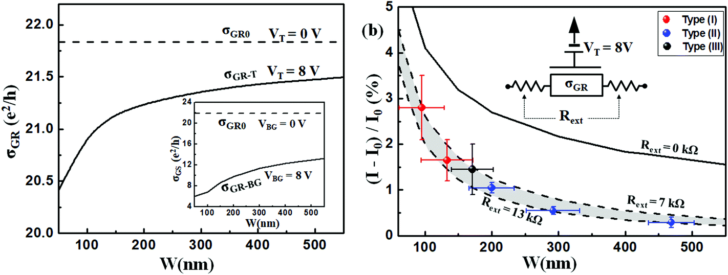 | ||
| Fig. 5 (a) Conductivities of the GR (σGR) as a function of width (W) on the application of either VT = 0 V (dashed line) or 8 V (solid line) marked with σGR0 or σGR-T, respectively. Inset: σGR as a function of W on the application of either VBG = 0 V (dashed line) or 8 V (solid line) marked with σGR0 or σGR-BG, respectively. (b) Current variation around (I − I0)/I0 as a function of the GR width from ∼95 nm to ∼470 nm and its theoretically fitted results on the application of VT = 8 V (dashed line). Here, (I − I0)/I0 for each width was extracted from the AFM and SGM images of GR type (I) (blue dots), type (II) (red dots), and type (III) (black dots) shown in Fig. 1, 2 and Fig. S3, S4.† Here, the calculated lines were extracted for the GR junction structure (dashed lines and the gray area) or the individual GR structure (solid line) with the parameters of Rext = 7 to 13 kΩ or 0 kΩ, respectively. Inset: Schematic diagram of the GR connected with the Rext structure on the application of VT. | ||
Conclusions
We studied the conductance variations in GR junctions under different widths and directions, and the Joule heating conditions under the application of different biases and gate voltages. While there were no effects observed due to the direction, the conductance and thermal variations of the GR junction varied between 2.8% and 0.29% and 24 K and 5 K, respectively; these values are minute for widths of 95 nm to 470 nm. Furthermore, we confirmed that the width dependency of the GR contributed directly to the conductance variation of the entire GR junction. This gate-tuned conductance variation of GR with sub-micrometer widths allows us to obtain a predictable and precise characterization of graphene electrodes for nanoscale interconnection applications in high-density array electronics.Experimental methods
Fabrication of GR FETs
To prepare the GR junction structure, single-layer graphene FETs were fabricated by mechanical exfoliation of Si wafers covered with ∼280 nm thick SiO2. Then Cr/Au electrodes (0.5 nm/40 nm thickness) were made to come into contact by standard e-beam lithography. For defining the dimensions of the GR junctions, we employed an e-beam resist of PMMA. By etching away the unprotected graphene area between the PMMA etch mask using oxygen plasma, we could isolate the GR junction area from the graphene flakes (see ESI, Fig. S1†). The GR junction devices were annealed at 320 °C to 360 °C in a hydrogen/argon gas mixture for two hours to remove the PMMA residue on the graphene surface. This manufacturing process allowed us to prepare various GR junction devices with widths ranging from ∼95 to ∼470 nm and lengths ranging from 4.0 to 5.5 μm (see also ESI, Fig. S2†).Scanning probe microscopy characterization
To elucidate the spatial formation tendencies of graphene, SPM measurements were performed using a commercial atomic force microscope (XE-100, Park Systems Corp.) in air at room temperature. While observing EFM data, we applied an AC voltage of amplitude ∼0.5 V, a DC voltage of 1 to 2 V, and a frequency of 17 kHz to a Cr/Au coated probe. The EFM images were obtained by a two-way scan method to avoid topographic artifacts. The first scan was for topography in the noncontact mode with a dithering resonant frequency of ∼120 to 170 kHz, and the second scan was for an EFM image using the ∼100 nm constant height mode. For observing the SGM image, we applied a gate voltage VTvia a metal-coated SPM probe at a constant height of ∼100 nm.27,28 Upon applying VT on individual GR areas, the conductance of the entire GR junction structure was observed by the normal 2-probe measurement between the electrodes at each end of the entire GR junction. Scanning thermal microscopy (SThM) experiments were carried out by monitoring the resistance variation of a high-resolution thermistor on the SPM tip connected to a Wheatstone bridge circuit. The resistance of the SThM probe was calibrated on an absolute-temperature scale by employing Raman spectroscopy of graphene that included the temperature of the G-mode phonon.28,36 First, we measured the SThM signal induced by the off-balance of the Wheatstone bridge signal under a graphene applied bias voltage. Then, the temperatures of the G-mode phonons (TG) of the graphene applied bias voltage were obtained from the ratio of the anti-Stokes and Stokes signals through the relationship IaS/IS = Cexp(−ħωG/kBTG), where ħωG is the G-phonon energy (∼195 meV), kB is the Boltzmann constant, and C is a previously determined numerical factor.36 Finally, by comparing the SThM signal and the TG of graphene under the same bias voltage, we calibrated the resistance unit of the SThM signal with the absolute-temperature unit.28
Conductivity model for graphene
We employed the following description of the conductivity of graphene in this work:where Δn,
 , ni, and n* are the gating (VT or VBG)-induced carrier density (externally induced), carrier density induced in graphene by the charged impurity (internal characteristic of graphene), charged impurity concentration, and self-consistent residual carrier density considering electron and hole puddle formation by the charged impurities, respectively.37,38 For a given ni, and n* were determined by the relationship:
where CRPA0(rs,a) = −1 + 4E1(a)/(2 + πrs)2 + 2e−ars/(1 + 2rs) + (1 + 2rsa)e2rsa(E1[2rsa] − E1[a(1 + 2rs)]) and

 (the exponential integral function). The effects of both dangling bonds on SiO2 and the undesired residues on the graphene surface leading to the doping of graphene were reflected in the variables rs ≈ 0.8 (graphene on a SiO2 substrate) and d ≈ 1 nm (distance between graphene and a plane where charged impurities lie).33,34 The above graphene conductivity description was established under the assumption of zero temperature. However, our graphene sample's Fermi level was approximately 188 meV for type (I) GR, which translated to a Fermi temperature of TF = EF/kB = 2187 K. Type (II) and (III) GRs also exhibited similar conditions. This was approximately seven times higher than room temperature (300 K). Therefore, the conductivity model described above was applicable to our study constructed under room temperature.37
Simulation of the gate (VT or VBG)-tuned conductance of GR
To simulate the GR with tip or back gating, we solved the Maxwell equations for electric potential under the electrostatic situation. We regarded graphene and Si substrate as a conductor and put the metallic tip above the GR (see ESI, Fig. S6†). By applying a gate voltage to the metallic tip surface or the Si substrate, the surface charges on graphene were acquired by differentiating the electric potential near the graphene surface. The calculated charges were regarded as additional carriers in graphene; thus, the conductivity of graphene formed a spatial distribution. The effective conductivity (averaged conductivity) of the GR could be expressed as follows:22where σlocal is the conductivity on the local area of graphene. Since our GR specimens were gate tuned, we marked the effective graphene conductivity as σGR-T, σGR-BG, and σGR0 for the applied gate voltages of VT (tip-gating), VBG (back-gating), and 0, respectively. The current was I = VDS/(RGR + Rext) and RGR = L/(W·σGR), we could extract the conductance of the GR and conductance variation as 1/RGR and (I − I0)/I0 = [{1/(W·σGR0) + L·Rext}/{1/(W·σGR-G) + L·Rext}] − 1, where L and W are the length and width of the GR, respectively.

Conflicts of interest
There are no conflicts to declare.Acknowledgements
This work was supported by an Institute for Information & Communications Technology Promotion (IITP) grant funded by the Korean government (MSIP) (2016-0-00576, Fundamental Technologies of Two-dimensional Materials and Devices for the Platform of New-functional Smart Devices) and the Basic Science Research Program through the National Research Foundation of Korea (NRF) funded by the Ministry of Education (NRF-2017R1A6A3A11034292).References
- A. K. Geim and I. V. Grigoreva, Nature, 2013, 499, 419–425 CrossRef CAS PubMed.
- L. Britnell, R. V. Gorbachev, R. Jail, B. D. Belle, F. Schedin, A. Mishchenko, T. Georgiou, M. I. Katsnelson, L. Eaves, S. V. Morozov, N. M. Peres, J. Leist, A. K. Geim, K. S. Novoselov and L. A. Ponomarenko, Science, 2012, 335, 947–950 CrossRef CAS PubMed.
- G.-H. Lee, Y.-J. Yu, X. Cui, N. Petrone, C.-H. Lee, M. S. Choi, D.-Y. Lee, C. Lee, W. J. Yoo, K. Watanabe, T. Taniguchi, C. Nuckolle, P. Kim and J. Hone, ACS Nano, 2013, 7, 7931–7936 CrossRef CAS PubMed.
- B. Radisavljevic, A. Radenovic, J. Brivio, V. Giacometti and A. Kis, Nat. Nanotechnol., 2011, 6, 147–150 CrossRef CAS PubMed.
- Q. H. Wang, K. Kalantar-Zadeh, A. Kis, J. N. Coleman and M. S. Strano, Nat. Nanotechnol., 2012, 7, 699–712 CrossRef CAS PubMed.
- O. Lopez-Sanchez, D. Lembke, M. Kayci, A. Radenovic and A. Kis, Nat. Nanotechnol., 2013, 8, 497–501 CrossRef CAS PubMed.
- C.-H. Lee, G.-H. Lee, A. M. van der Zande, W. Chen, Y. Li, M. Han, X. Cui, G. Arefe, C. Nuckolls, T. F. Heinz, J. Guo, J. Hone and P. Kim, Nat. Nanotechnol., 2014, 9, 676–681 CrossRef CAS PubMed.
- K. Kang, S. Xie, L. Huang, Y. Han, P. Y. Huang, K. F. Mak, C.-J. Kom, D. Muller and J. Park, Nature, 2015, 520, 656–660 CrossRef CAS PubMed.
- X. Chen, Y. Wu, Z. Wu, Y. Han, S. Xu, L. Wang, W. Ye, T. Han, Y. He, Y. Cai and N. Wang, Nat. Commun., 2015, 6, 7315 CrossRef CAS PubMed.
- L. Yu, Y.-H. Lee, X. Ling, E. J. G. Santos, Y. C. Shin, Y. Lin, M. Dubey, E. Kaxiras, J. Kong, H. Wang and T. Palacios, Nano Lett., 2014, 14, 3055–3063 CrossRef CAS PubMed.
- X. Cui, G.-H. Lee, Y. D. Kim, G. Arefe, P. Y. Huang, C.-H. Lee, D. A. Chenet, X. Zhang, L. Wang, F. Ye, F. Pizzocchero, B. S. Jessen, K. Watanabe, T. Taniguchi, D. A. Muller, T. Low, P. Kim and J. Hone, Nat. Nanotechnol., 2015, 10, 534–540 CrossRef CAS PubMed.
- G.-H. Lee, X. Cui, Y. D. Kim, G. Arefe, X. Zhang, C.-H. Lee, F. Ye, K. Watanabe, T. Taniguchi, P. Kim and J. Hone, ACS Nano, 2015, 9, 7019–7026 CrossRef CAS PubMed.
- C. R. Dean, A. F. Young, I. Meric, C. Lee, L. Wang, S. Sorgenfrei, S. Watanabe, T. Taniguchi, P. Kim, K. L. Shepard and J. Hone, Nat. Nanotechnol., 2010, 5, 722–726 CrossRef CAS PubMed.
- L. Wang, I. Meric, P. Y. Huang, Q. Gao, Y. Gao, H. Tran, T. Takashi, W. Kenji, L. M. Campos, S. A. Muller, J. Guo, P. Kim, J. Hone, K. L. Shepard and C. R. Dean, Science, 2013, 342, 614–617 CrossRef CAS PubMed.
- S. J. Kang, G.-H. Lee, Y.-J. Yu, Y. Zhao, B. Kim, J. Hone, P. Kim and C. Nuckolls, Adv. Funct. Mater., 2014, 24, 5157–5163 CrossRef CAS.
- A. Pospischil, M. Humer, M. M. Furchi, D. Bachmann, R. Guider, T. Fromherz and T. Mueller, Nat. Photonics, 2013, 7, 892–896 CrossRef CAS.
- F. H. L. Koppens, M. P. Avouris, A. C. Ferrari, M. S. Vitilello and M. Polioni, Nat. Nanotechnol., 2014, 9, 780–793 CrossRef CAS PubMed.
- F. Xia, H. Wang, D. Xia, M. Dubey and A. Ramasubramaniam, Nat. Photonics, 2014, 8, 899–907 CrossRef CAS.
- C.-H. Liu, Y.-C. Chang, T. B. Norris and Z. Zhong, Nat. Nanotechnol., 2014, 9, 273–278 CrossRef CAS PubMed.
- M. Y. Han, B. Özyilmaz, Y. Zhang and P. Kim, Phys. Rev. Lett., 2007, 98, 206805 CrossRef PubMed.
- M. Y. Han, J. C. Brant and P. Kim, Phys. Rev. Lett., 2010, 104, 056801 CrossRef PubMed.
- E. T. Vasko and I. V. Zozoulenko, Appl. Phys. Lett., 2010, 97, 092115 CrossRef.
- A. Venugopal, J. Chan, X. Li, C. W. Magnuson, W. P. Kirk, L. Colombo, R. S. Ruoff and E. M. Vogel, J. Appl. Phys., 2011, 109, 104511 CrossRef.
- C. Smith, R. Qaisi, Z. Liu, Q. Yu and M. M. Hussain, ACS Nano, 2013, 7, 5818–5823 CrossRef CAS PubMed.
- M. J. Hollander, H. Madan, N. Shukla, D. A. Snyder, J. A. Robinson and S. Datta, Appl. Phys. Express, 2014, 7, 055103 CrossRef.
- V. Panchal, A. Lartsev, A. Manzin, R. Yakimova, A. Tzalenchuk and O. Kazakova, Sci. Rep., 2014, 4, 588 Search PubMed.
- C. Stampfer, J. Güttinger, S. Hellmüller, F. Mlitor, K. Ensslin and T. Ihn, Phys. Rev. Lett., 2009, 102, 056403 CrossRef CAS PubMed.
- Y.-J. Yu, M. Y. Han, S. Berciaud, A. B. Georgescu, T. F. Heinz, L. E. Brus, K. S. Kim and P. Kim, Appl. Phys. Lett., 2011, 99, 183105 CrossRef.
- I. Jo, I.-K. Hsu, Y. J. Lee, M. M. Sadeghi, S. Kim, S. Cronin, E. Tutuc, S. K. Banerjee, Z. Yao and S. Li, Nano Lett., 2011, 11, 85–90 CrossRef CAS PubMed.
- Y.-J. Yu, Y. Zhao, S. Ryu, L. E. Brus, K. S. Kim and P. Kim, Nano Lett., 2009, 9, 3430–3434 CrossRef CAS PubMed.
- S. Sorgenfrei, C. Chiu, R. L. Gonzalez, Y.-J. Yu, P. Kim, C. Nuckolls and K. L. Shepard, Nat. Nanotechnol., 2011, 6, 126–132 CrossRef CAS PubMed.
- G. H. Lee, Y.-J. Yu, C. Lee, C. Dean, K. L. Shepard, P. Kim and J. Hone, Appl. Phys. Lett., 2011, 99, 243114 CrossRef.
- X. Du, I. Skachko, A. Barker and E. Y. Andrei, Nat. Nanotechnol., 2008, 3, 491–495 CrossRef CAS PubMed.
- A. S. Mayorov, R. V. Gorbachev, S. V. Morozov, L. Britnell, R. Jalil, L. A. Ponomarenko, P. Blake, K. S. Novoselov, K. Watanabe, T. Taniguchi and A. K. Geim, Nano Lett., 2011, 11, 2396–2399 CrossRef CAS PubMed.
- F. Giannazzo, S. Sonde, R. L. Nigro, E. Rimini and V. Raineri, Nano Lett., 2011, 11, 4612–4618 CrossRef CAS PubMed.
- S. Berciaud, M. Y. Han, K. F. Mak, L. E. Brus, P. Kim and T. F. Heinz, Phys. Rev. Lett., 2010, 104, 227401 CrossRef PubMed.
- S. Adam, E. H. Hwang, V. M. Galitski and S. A. Das Sarma, Proc. Natl. Acad. Sci. U. S. A., 2007, 104, 18392–18397 CrossRef CAS PubMed.
- Y.-W. Tan, Y. Zhang, K. Bolotin, Y. Zhao, S. Adam, E. H. Hwang, S. Das Sarma, H. L. Stormer and P. Kim, Phys. Rev. Lett., 2007, 99, 246803 CrossRef PubMed.
Footnotes |
| † Electronic supplementary information (ESI) available. See DOI: 10.1039/c8nr10469g |
| ‡ These authors contributed equally to this work. |
| This journal is © The Royal Society of Chemistry 2019 |