
 Open Access Article
 This Open Access Article is licensed under a Creative Commons Attribution-Non Commercial 3.0 Unported Licence
Scalable fabrication of high-quality crystalline and stable FAPbI3 thin films by combining doctor-blade coating and the cation exchange reaction†
Sampson
Adjokatse
 ,
Hong-Hua
Fang
,
Herman
Duim
and
Maria Antonietta
Loi
*
,
Hong-Hua
Fang
,
Herman
Duim
and
Maria Antonietta
Loi
*
Zernike Institute for Advanced Materials, University of Groningen, Nijenborgh 4, 9747 AG, Groningen, The Netherlands. E-mail: m.a.loi@rug.nl
First published on 15th March 2019
Abstract
Formamidinium lead iodide (FAPbI3) is one of the most extensively studied perovskite materials due to its narrow band gap and high absorption coefficient, which makes it highly suitable for optoelectronic applications. Deposition of a solution containing lead iodide (PbI2) and formamidinium iodide (FAI) or sequential deposition of PbI2 and FAI usually leads to the formation of films with a poor morphology and an unstable crystal structure that readily crystallize into two different polymorphs: the photoinactive yellow phase and the photoactive black phase. In this work, 2D 2-phenylethylammonium lead iodide (PEA2PbI4) thin films are deposited by a scalable doctor-blade coating technique and used as a growth template for the high-quality 3D FAPbI3 perovskite thin films which are obtained by organic cation exchange. We report the structural, morphological and optical properties of these converted 3D FAPbI3 perovskite films which we compare to the directly deposited 3D FAPbI3 films. The converted FAPbI3 thin films are compact, smooth, and highly oriented and exhibit better structural stability in comparison with the directly deposited 3D films. These results not only underscore the importance of the employed deposition techniques in fabricating highly crystalline and stable perovskite thin films but also provide a strategy to easily obtain very compact perovskite layers using doctor-blade coating.
Introduction
Organic–inorganic metal halide perovskite semiconductors are of very high interest to the semiconductor community due to their superior photophysical properties and their ever-increasing significance for optoelectronic and other electronic applications.1–4 Thin films of metal halide perovskites have been used extensively as light absorbers in photovoltaics5–8 with a certified record power conversion efficiency (PCE) of 23.7%.9 Other optoelectronic devices in which perovskite semiconductors have been investigated and that have demonstrated outstanding performances include light-emitting diodes,10–12 light-emitting field-effect transistors,13–16 lasers,17–20 photodetectors21–25 and X-ray detectors.26,27One of the key factors central to the demonstrated device performances is the perovskite film quality. This includes the morphology, crystallinity and phase purity. In the last few years, the most used deposition method has been the one-step solution processing technique, which involves direct deposition of a solution containing the perovskite precursors, typically lead halide (PbX2, X = I−, Br−, or Cl−) and methylammonium halide (MAX) or formamidinium halide (FAX).3,28 This technique results in the formation of thin films with a poor surface coverage, a large surface roughness and often unreacted PbX2 residues, with negative consequences for the performance and stability of devices.29 To enhance the perovskite film quality, deposition techniques such as the two-step sequential deposition, vapor-assisted deposition, and thermal vapor deposition techniques have been developed.30–34 Other techniques such as solvent engineering,35–37 solvent additives38 or temperature-assisted rapid nucleation39 and process engineering methods like anti-solvent treatment,40 solvent annealing41 and hot-casting42 have all been developed in order to control the film morphology and its quality in general.
An important problem is that the quality of the films deposited by these techniques is strongly dependent on the material composition and the solvent used, which is one of the main reasons for the large proliferation of deposition techniques. For instance, while high-quality perovskite films of methylammonium lead iodide (MAPbI3) have been prepared using most of the abovementioned advanced processing techniques, only the sequential deposition method has given satisfactory formamidinium lead iodide (FAPbI3) thin films.43–47
FAPbI3 is a highly interesting material because of its band gap (∼1.48 eV) and its enhanced thermal stability compared to the widely used MAPbI3. However, the ionic radius and symmetry of the FA+ cation make the FAPbI3 perovskite structurally unstable as it can readily crystallize into two different polymorphs at room temperature: the undesired photoinactive “yellow” δ-phase (δ-FAPbI3) and the desired photoactive “black” α-phase (α-FAPbI3).47,48 Thus, new strategies are required to fabricate and scale up high-quality FAPbI3 thin films with improved morphology and structural stability, which could lead to enhanced optoelectronic properties, both in terms of performances and stability.
Recently, an avalanche of new processing techniques has been employed to control and grow high-quality perovskite thin films and to tune their composition. One such technique is the incorporation of dopants such as Cs to structurally stabilize FAPbI3 as demonstrated by Zhu and co-workers.49 An alternative technique is the ion exchange reaction, which is a well-known method for engineering material composition, creating alloys or obtaining controlled doping.50 MAPbI3 thin films with high surface coverage, smoothness and crystallinity have been successfully fabricated using various starting materials as thin film growth templates.51–54 Similarly, using HPbI3, NH4PbI3,55 MAPbI3![[thin space (1/6-em)]](https://www.rsc.org/images/entities/char_2009.gif) 56etc. as growth templates, various groups have demonstrated the fabrication of phase-pure α-FAPbI3 thin films with enhanced film quality. Eperon et al. have also successfully demonstrated the exchange of the B-site metal cation by partial or full substitution of the tin (Sn) in formamidinium tin iodide (FASnI3) with lead (Pb).57 Jen and co-workers recently used a 2D perovskite, namely, phenylethylammonium lead bromide (PEA2PbBr4), as a growth template, obtaining highly oriented, high-quality 3D methylammonium lead bromide (MAPbBr3) thin films.58
56etc. as growth templates, various groups have demonstrated the fabrication of phase-pure α-FAPbI3 thin films with enhanced film quality. Eperon et al. have also successfully demonstrated the exchange of the B-site metal cation by partial or full substitution of the tin (Sn) in formamidinium tin iodide (FASnI3) with lead (Pb).57 Jen and co-workers recently used a 2D perovskite, namely, phenylethylammonium lead bromide (PEA2PbBr4), as a growth template, obtaining highly oriented, high-quality 3D methylammonium lead bromide (MAPbBr3) thin films.58
At this point, it is important to underline that all these techniques are based on a spin coating step and are difficult or impossible to scale up, which is a bottleneck towards the exploitation of hybrid perovskites in technology. Given the need for solution-based thin film deposition techniques that are simple, low-cost and compatible with industrial-scale fabrication, in this work we demonstrate an industrially relevant deposition pathway giving rise to high quality hybrid perovskite thin films. This deposition pathway combines the advantages of doctor-blade coating and the ion exchange reaction method to fabricate high-quality phase-pure α-FAPbI3 perovskite thin films that are structurally stable and highly crystalline. Phenylethylammonium lead iodide (PEA2PbI4) perovskite thin films are doctor-blade coated and fully converted to α-FAPbI3 upon immersing the 2D layer in a FAI solution. The choice of PEA2PbI4 as our starting material is based on its good film formability on different substrates even when deposited using different deposition techniques, including scalable blade coating. For comparison, one-step doctor-blade coated FAPbI3 thin films are also investigated. The structural, morphological and optical characterization shows that the converted thin films exhibit unprecedented film quality, with preferential crystallographic orientation and enhanced ambient stability compared to the one-step deposited films. These results underline the immense potential of combining the scalable doctor-blade coating and the ion exchange reaction technique in the growth of stable and high-quality perovskite thin films.
Experimental
Materials and solution preparation
The perovskite precursors lead(II) iodide (PbI2) (99.99%), 2-phenylethylammonium iodide (C6H5C2H4NH3I, PEAI) (>98%) and formamidine hydroiodide (FAI) (>98%) were purchased from TCI EUROPE N.V. and used as received without further purification. N,N′-Dimethylformamide (DMF) (99.8%) was acquired from Sigma-Aldrich and dimethyl sulfoxide (DMSO) (99.9%) from Alfa Aesar.The 2D PEA2PbI4 perovskite precursor solution was prepared by dissolving PEAI and PbI2 at a molar ratio of 2:1 in a mixed solvent of DMF and DMSO at a volume ratio of 4:1 to form a solution of 0.5 M concentration. The 3D FAPbI3 perovskite precursor solution was prepared by dissolving FAI and PbI2 at a molar ratio of 1:1 also in a mixed solvent of DMF and DMSO at a volume ratio of 4:1 to form a solution of 1 M concentration. The solutions were stirred for at least 3 hours at room temperature before deposition. The organic precursor solution was prepared by dissolving FAI in isopropyl alcohol (IPA) to form a solution with a concentration of 20 mg mL−1.
Perovskite film fabrication
The films were fabricated on glass substrates, which were ultrasonically cleaned in detergent solution, deionized water, acetone and isopropanol, sequentially. After drying them in an oven at 140 °C for about 10 min, they were treated with ultraviolet ozone (UV-O3) for 20 min and then transferred to a nitrogen-filled glove box immediately for film deposition.The perovskite growth process involved the transformation of the pure 2D perovskite PEA2PbI4 into the desired 3D FAPbI3 perovskite thin film by the ion exchange method. The 2D films were fabricated using the spin coating and doctor blade coating techniques. The spin coated 2D samples were fabricated using a two-step spin program with anti-solvent treatment. The spin program was set at 1000 rpm for 10 s and 4000 rpm for 30 s. The anti-solvent (chlorobenzene) was added dropwise to the film about 10 s prior to the end of spinning. The films were immediately annealed at 100 °C for 10 min. For the doctor blade coating process, the precursor solution was added dropwise to the substrate and swiped linearly by a metal blade as depicted in Fig. 1. The optimized 2D films were blade coated on glass substrates held at 80 °C by swiping the precursor solution with the blade at a speed of 10 mm s−1. The gap between the glass substrate and the blade was fixed at 400 μm. The films were immediately annealed at 100 °C for 10 min. The optimized reference 3D FAPbI3 perovskite film was also blade coated at a temperature of 90 °C at a blade speed of 40 mm s−1 and a fixed gap of 400 μm. The film was annealed at 160 °C for at least 30 min. To convert the 2D perovskite to 3D, the 2D film was dipped in 20 mg mL−1 FAI in an IPA solution for ∼3 min and then rinsed in IPA for ∼30 s in order to wash away the dangling PEA+ ions on the surface of the film and subsequently dried by spinning. No further annealing was needed to drive the 3D conversion to full completion.
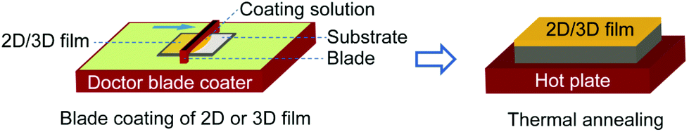 | ||
| Fig. 1 Schematic illustration of the doctor-blade setup used for the deposition of the 2D PEA2PbI4 and reference 3D FAPbI3 perovskite films. | ||
Morphological characterization
The scanning electron microscopy (SEM) images were obtained using a FEI Nova Nano SEM 650 instrument with an accelerating voltage of 2–10 kV for the secondary electron images and ∼10 kV for the backscattered electron images. The atomic force microscopy (AFM) images were taken using a Bruker NanoScope V instrument in the ScanAsyst mode.Reflected light micrographs were recorded using an Olympus BX51 M microscope equipped with a ColorView CCD camera and Plan Fluor objectives at 5×, 10× and 50× magnifications.
Structural characterization
The X-ray diffraction experiment was performed under ambient conditions using a Bruker D8 Advance diffractometer operated in the Bragg–Brentano geometry and equipped with a Cu Kα radiation source (λ = 1.54 Å) and a LynxEye detector.Optical characterization
Absorption measurements were taken using a UV-vis-NIR spectrophotometer (Shimadzu UV-3600). The photoluminescence measurements were performed using the second harmonic (400 nm) of a Ti:sapphire laser (repetition rate, 76 MHz; Mira 900, Coherent) to excite the samples. The illumination power could be adjusted using a variable neutral density filter. The excitation beam was spatially limited using an iris and focused with a 150 mm focal length lens. Emitted photons were collected with a lens and directed to a spectrograph. Steady-state spectra were collected using a Hamamatsu EM-CCD camera.Confocal laser scanning microscopy (CLSM) measurements were performed using a Nikon Eclipse Ti microscope. Samples were excited using Ar+ ions with an excitation wavelength of 488 nm. The excitation beam was focused on the sample using a 100× (oil immersion Plan Apo) objective. Spatial mapping of the photoluminescence was obtained by raster scanning the sample and recording the PL signal using a 650 nm long pass detection channel.
Results and discussion
2D PEA2PbI4 perovskite thin films are fabricated from a solution containing 2-phenylethylammonium iodide (PEAI) and PbI2 in a solvent mixture of N,N′-dimethylformamide (DMF) and dimethyl sulfoxide (DMSO) using both the spin coating and doctor-blade coating techniques. Unlike the 3D perovskites, this 2D material exhibited good film formability even when deposited using the one-step solution deposition technique. Fig. 1 shows a schematic diagram of the deposition procedure for the doctor-blade coating technique. The detailed fabrication procedure of the 2D films using both the spin-coating and doctor-blade coating methods is described in the Experimental section.The structure, morphology and band gap of the prepared thin films are examined using X-ray diffraction (XRD), atomic force microscopy (AFM) and UV-Vis spectroscopy, respectively. The two deposition techniques result in thin films with similar XRD patterns and absorption profiles but very different morphologies. As is shown in Fig. S1a,† the XRD patterns of the two samples exhibit similar diffraction peaks with preferential orientation at 2θ values of 5.45°, 10.88°, 16.30°, 21.79°, 27.29°, 32.92° and 38.56°. However, the doctor-blade coated film exhibits more than three orders of magnitude stronger peak intensity compared to the spin coated film. This proves the higher crystallinity of the doctor-blade coated film.
The absorption spectra of these thin films closely resemble those previously reported with an excitonic peak at 515 nm.59 The doctor-blade coated film, however, has a higher absorbance than the spin-coated film, implying that the film is thicker and/or has better surface coverage (Fig. S1b†).
The morphological properties of the films are characterized using atomic force microscopy (AFM). While the spin coated film shows high inhomogeneity and roughness with surface grains of nanometer size, the doctor-blade coated film is flatter and smoother and has crystalline domains that are as large as 15 μm as is evident from Fig. S1c and S1d,† respectively. The surface roughness of these films extracted from the AFM images are 22 and 50 nm in favor of the doctor-blade coated film.
The 2D perovskite films are dipped in a solution containing FAI dissolved in isopropyl alcohol (IPA) to convert them into 3D FAPbI3 perovskite by the ion (organic-cation) exchange reaction. The approach follows previous studies, where various 2D perovskites were used as the starting materials to grow multidimensional (2D/3D)60 or 3D53,54,58 hybrid perovskites. A schematic diagram of the ion exchange reaction process is depicted in Fig. 2a. Photographs of the 2D perovskite films before and after conversion to 3D films without and with rinsing in IPA are shown in Fig. 2b–d. We observed that without the washing steps in IPA, the 3D perovskite film degrades immediately after drying (Fig. 2c), while the washed samples remain stable for many days. This observation shows that the exchange reaction is kinetically driven, and in the absence of the washing step, it will be thermodynamically driven backwards to the starting material. We therefore attribute this unstable behaviour of the unwashed samples to the presence of long organic ligands on the surface of the film, which readily promotes further reactions that are detrimental to the stability of the converted 3D perovskite film.
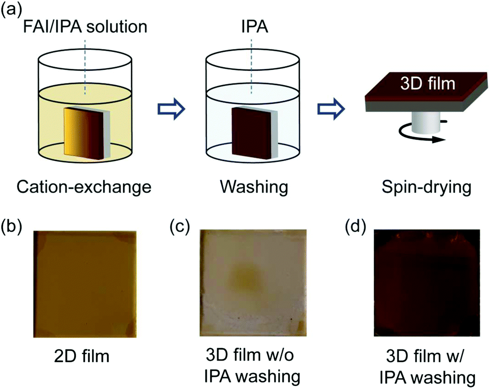 | ||
| Fig. 2 (a) Schematic illustration of 2D-to-3D conversion by the cation exchange reaction. (b) Photographs of the spin-dried 2D perovskite film, (c) the converted 3D perovskite film without the washing step in isopropyl alcohol (IPA) and (d) the converted 3D perovskite film with the washing step in IPA. | ||
To study the kinetics of the cation exchange in more detail, we performed an in situ conversion experiment. At time t = 0, a FAI/IPA ligand solution is injected into a cuvette containing the 2D perovskite film to initiate the 2D-to-3D conversion while simultaneously monitoring the photoluminescence (PL) of the sample. Fig. 3a shows the PL emission evolution of the conversion taken at 1 second time interval. Initially, only a narrow peak of the 2D perovskite at 530 nm is observed. The PL intensity of this 2D peak increases in the first second after adding the ligand solution but then vanishes almost completely within another 10 seconds. At the same time, a much broader PL peak originating from the 3D FAPbI3 emerges around 800 nm. The emission from the 3D perovskite shows a rapid decrease in PL intensity and a considerable red-shift in the first seconds after its appearance. A detailed analysis of the dynamics of the 3D peak can be found in the ESI (Fig. S2a and S2b†). After the appearance of the feature at around 800 nm, a minimum PL intensity is reached after 40 seconds as shown in Fig. S2a.† After this local minimum, the intensity steadily increases again while the peak continues to exhibit a small monotonic red-shift (Fig. S2b†). This red-shift is most likely caused by the conversion of low-dimensional perovskite intermediates to the 3D perovskite phase. It is important to underline that an eventual PL signal from the 2D and other low-dimensional perovskite phases, after the start of the conversion towards the 3D perovskite phase, will not be directly detectable because of reabsorption and energy transfer. The slow recovery of PL in the final stage of the conversion process is considered to be the result of further growth of the 3D domains and minimization of defects through laser-induced healing.
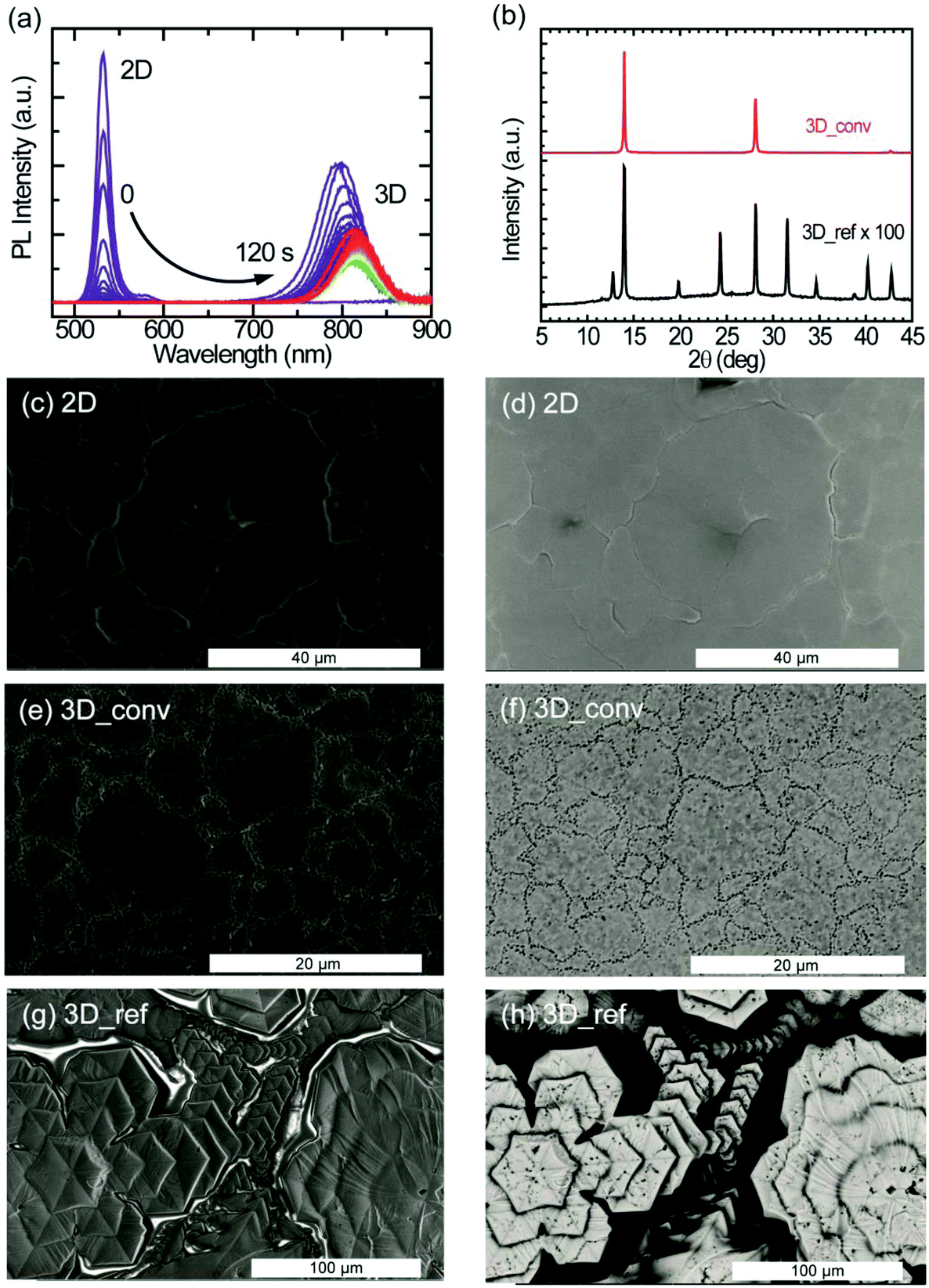 | ||
| Fig. 3 2D–3D conversion kinetics and structural and morphological characterization of the converted and reference 3D perovskite films, all fabricated by the doctor-blade coating technique. (a) In situ photoluminescence (PL) emission spectra showing the conversion kinetics of the evolution from 2D to 3D perovskites, (b) X-ray diffraction patterns of the converted and the reference film fabricated by doctor-blade coating. (c–h) Four SEM images showing the surface topography and compositional properties of the 2D PEA2PbI4, the converted and the reference 3D FAPbI3 perovskite films. (c, e and g) Secondary electron and (d, f and h) backscattered electron images of the 2D, converted and reference 3D perovskite films, respectively. | ||
After the full conversion from 2D to 3D, the films are characterized to investigate the quality of the films. The comparison of the converted 3D films based on the spin coated and doctor-blade coated 2D films shows that the latter exhibit better film properties, mimicking the quality of the 2D films. The structural and morphological characteristics of the converted film based on the spin coated 2D film are shown in Fig. S3 of the ESI.† As a reference for the converted films based on the doctor-blade coated 2D films, 3D FAPbI3 thin films were doctor-blade coated on a glass substrate.
The XRD patterns illustrating the structural properties of the converted and reference 3D perovskite films fabricated by doctor-blade coating are displayed in Fig. 3b. Compared to the reference film, the converted films exhibit highly oriented crystal domains with characteristic peaks at 2θ values of 13.97°, 28.13° and 42.71°, corresponding to scattering from (111), (222) and (333) crystal planes. The reference film, on the other hand, exhibits additional diffraction peaks at 12.74°, 19.79°, 24.30°, 31.56°, 34.65°, 38.81° and 40.22°, which correspond to randomly arranged crystal planes. Although no signature peak of the photoinactive (δ-phase) perovskite is observed in both films, the characteristic peak from PbI2 (12.74°), which is a result of the rapid degradation of the sample in air, is observed in the reference film. The diffraction peaks from the converted films are about two orders of magnitude stronger in intensity than that of the reference film. In Fig. 3b, the peak intensity of the reference film is magnified by a factor of 100 for the purpose of illustration. The FWHM of the characteristic peak at 13.97° is 0.14° and 0.21° for the converted and the reference sample, respectively. This shows that the converted perovskite film has better crystallinity and a lower level of disorder with respect to the reference sample. It's worth mentioning, at this point, that no diffraction peaks from the 2D perovskite are observed in the diffraction pattern of the converted film.
As explained above, the morphological quality of thin films defines the success of a deposition technique. SEM images portraying the film topography (secondary electrons) and the composition (backscattered electrons) of the 2D, converted 3D and the reference 3D perovskite films are shown in Fig. 3. In Fig. 3c, the secondary electron image of the 2D perovskite depicts a continuously smooth and homogeneous film with excellent surface coverage and very large crystalline domains (>10 μm), consistent with that seen in the AFM images. The uniform brightness of the backscattered electron images also reflects the highly uniform compositional distribution of the 2D film (Fig. 3d). These morphological features are directly translated into the converted 3D films except for the domain sizes, which appear smaller (>3 μm), and the presence of pinhole-like features at the domain boundaries as shown in Fig. 3e and f for the secondary electron and backscattered electron images, respectively. SEM images showing a wider view of the converted film are shown in Fig. S4.† The roughness of the converted 3D film as extracted from the AFM topographical image (Fig. S5†) is approximately 40 nm. Interestingly, laser scanning confocal microscopy measurements performed on the converted film show that the pitted domain boundaries have brighter photoluminescence (see Fig. S6†). In stark contrast, the topographical image of the 3D reference film in Fig. 3g shows the formation of hexagonal-like crystalline domains, resulting in a non-uniform film. As revealed in the backscattered electron image of Fig. 3h, the surface coverage of the film is very poor.
The absorbance spectra of the converted and reference 3D FAPbI3 perovskite films are shown in Fig. 4a. The spectra are normalized at 840 nm to aid in the comparison of the spectral shape and estimation of the band-edge (see Fig. 4b). The films have an absorption band-edge of around 830 nm, confirming the formation of the 3D FAPbI3 perovskite. However, the spectral profiles of the films are very different. The converted film has a characteristic absorption profile that depicts a continuous increase in light absorption from the near-infrared (NIR) to the visible region while the reference film shows almost constant light absorption in the same range. Moreover, as is shown in Fig. 4a, the reference film has a very high background signal in the NIR region compared to the converted film. These features are directly related to the film quality, specifically, the degree of surface coverage and homogeneity. While the observed high background absorption from the reference film is attributed to the high inhomogeneity of the film, which gives rise to a large scattering of the incident light, the flattening of the spectrum is attributed to poor surface coverage. These observations are in agreement with previous studies by Tian et al., where the correlations between the absorption spectral shapes and surface coverage and inhomogeneity of MAPbI3 perovskite thin films are examined.61
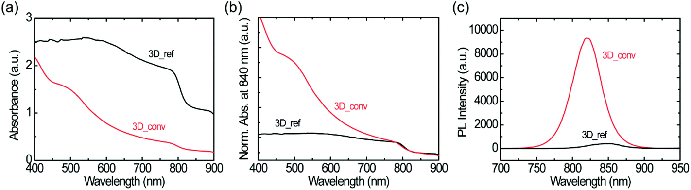 | ||
| Fig. 4 Optical characterization of converted and reference 3D perovskite films on glass substrates. (a–b) UV-vis absorbance spectra without normalization (a) and with normalization at 840 nm (b), (c) steady-state PL spectra. Note that 3D_ref and 3D_conv as indicated in the figures denote the reference one-step coated and converted FAPbI3 perovskites, respectively. | ||
Fig. 4c shows the photoluminescence spectra of both the reference and the converted film upon excitation with a 400 nm laser. The converted film shows a PL intensity that is over 20 times higher than that of the reference film. This large difference in PL intensity has two main causes; firstly, as mentioned before, the converted film shows much higher surface coverage than the reference film. Therefore, more photons are absorbed in the converted film and the PL intensity scales accordingly. Secondly, as the quality of the converted film is better than that of the reference film, it is to be expected that the excited charge carriers suffer less from non-radiative recombination in this film. This notion is further confirmed by the large red-shift of the PL spectrum of the reference film (845 nm) with respect to that of the converted film (823 nm); such a red-shift is typically associated with a high density of trap states.58
At this point, it is interesting to determine whether the stability of the material is also affected by the preparation method. The stability under ambient conditions is evaluated by probing the changes in the absorbance of the films under a relative humidity (RH) of 40–50% and a temperature of ∼23 °C. It is worth noting that the stability test under ambient conditions is performed on several films and a clear influence of the film degradation over time on the quality of the film is found. Photographs of the most stable converted and reference films stored in air over a period of 21 days are presented in Fig. 5a. Whereas the best reference film degraded rapidly within a day with consequent severe color bleaching, the best converted sample showed minimal degradation with negligible change in color even after 15 days. We attribute the degradation to the penetration of moisture at the grain or domain boundaries. The corresponding absorbance spectra of the films are shown in Fig. 5b and c for the reference and converted films, respectively. The absorbance of the reference film dropped drastically on the second day and as shown, no absorption peak was observed after 15 days. In contrast, the converted film, as already indicated by the photographs, maintained a high absorbance value without spectral modification for 21 days as shown in Fig. 5c.
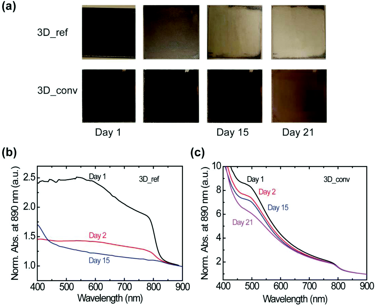 | ||
| Fig. 5 Characterization of the moisture stability of the reference and converted 3D FAPbI3 perovskite films under ambient conditions. (a) Photographs showing the evolution of the color of the reference (top) and converted (bottom) perovskite films over a 21 day period. (b and c) UV-vis absorbance spectra of the reference (b) and the converted (c) films normalized at 890 nm. | ||
Furthermore, the stability under illumination of both the converted 3D and reference films was assessed by exposing them to a focused laser beam of 400 nm (2.5 μJ cm−2) wavelength under ambient conditions. Fig. 6 displays color maps of the PL spectra as a function of exposure time for (a) the 3D reference sample and (b) the converted film. PL spectra at selected time intervals are plotted alongside (c) and (d). It is evident from these plots that the films behave distinctly differently under illumination. In the case of the reference 3D film, the low PL initially increases due to the laser-induced healing of trap states, which is accompanied by a slight blue-shift of the emission. After this initial healing stage, however, degradation begins and the intensity steadily drops until the signal reaches about 20% of its maximum intensity. During this degradation phase, a broad emission feature gradually arises at high energy, as is highlighted in the inset of Fig. 6c. We assign this feature to degradation products of FAPbI3, the most likely being PbI2, resulting from evaporation of the volatile organic cation as observed in the case of MAPbI3.62,63 At the laser excitation point, the decomposition of the perovskite is visible to the naked eye as a yellow spot. A cross-polarized light micrograph showing the strong change in birefringence of this degraded spot is shown in the ESI (Fig. S7†). In stark contrast to this, the converted film only shows a steady decrease in PL intensity and no degradation byproduct can be observed under the same excitation conditions. Moreover, it should be noted that even after prolonged laser illumination, the final PL intensity of the converted film is still considerably higher than the maximal value that the reference film ever reaches, which again highlights the superior quality of the converted films. Furthermore, the substantially higher PL intensity, narrower FWHM and the blue-shifted emission wavelength as shown in Fig. S8† all indicate the superior quality of the converted film with respect to the reference film.
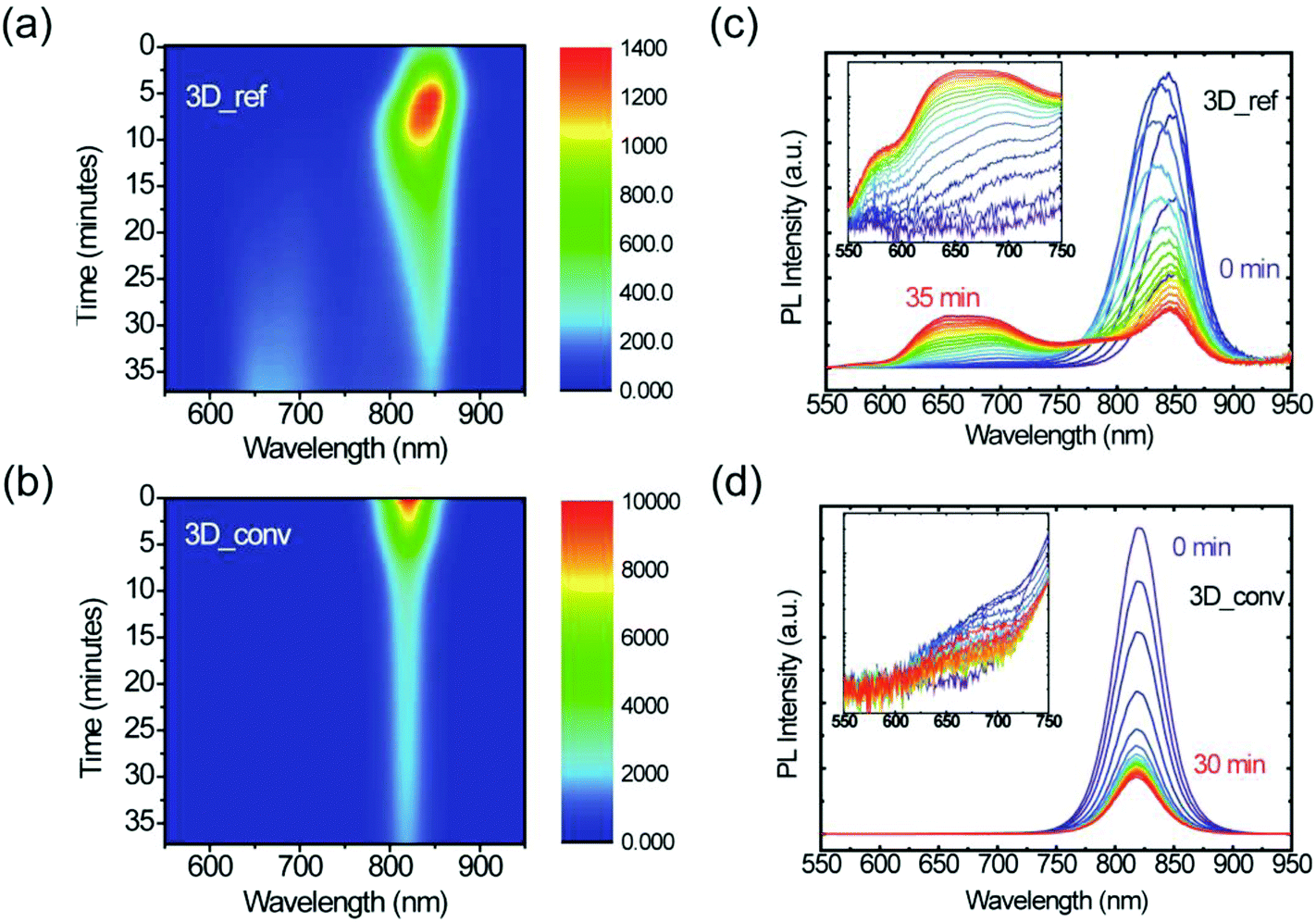 | ||
| Fig. 6 Photostability of the reference and converted 3D FAPbI3 perovskite films. (a) 2D pseudo-color plot of the PL spectra of the reference film as a function of continuous laser excitation time. (b) 2D pseudo-color plot of the PL spectra of the converted film as a function of continuous laser excitation time. (c) Evolution of the PL spectra of the reference film. (d) Evolution of the PL spectra of the converted film. | ||
We can therefore conclude that the herein reported conversion mechanism from a highly crystalline 2D film gives rise to highly oriented 3D films with superior ambient and photo-stability.
Conclusions
In summary, doctor-blade coated 2D 2-phenylethylammonium lead iodide (PEA2PbI4) films were employed as a growth template to fabricate high-quality photoactive 3D FAPbI3 thin films using a cation exchange reaction. The resultant perovskite film exhibits better film formability, excellent surface coverage and improved morphology with crystalline domain sizes as large as ∼10 μm. XRD patterns of the converted 3D perovskite film reveal very high crystallinity and a highly preferential orientation that mimics the orientation of the 2D perovskite template. The improved perovskite film leads to enhanced photoluminescence intensity, about 20 times higher than that of the reference one-step blade-coated FAPbI3 perovskite film. Furthermore, stability studies under continuous laser illumination and under ambient conditions show that the converted film exhibits significantly enhanced photo- and moisture stability compared to the reference film. The enhanced optoelectronic quality and high stability of the phase-pure FAPbI3 perovskite thin films obtained by the cation exchange reaction of a doctor-blade coated thin film are of extreme importance for the engineering and stabilization of perovskite thin films for optoelectronic applications.Conflicts of interest
There are no conflicts to declare.Acknowledgements
We would like to acknowledge technical support from Arjen Kamp and Teodor Zaharia. S. Adjokatse acknowledges financial support from The Netherlands Organization for Scientific Research (NWO Graduate Programme 2013, No. 022.005.006). We would also like to acknowledge funding from the European Research Council (ERC Starting Grant “Hy-SPOD” No. 306983) and the Foundation for Fundamental Research on Matter (FOM), which is part of the Netherlands Organisation for Scientific Research (NWO), under the framework of the FOM Focus Group “Next Generation Organic Photovoltaics”.Notes and references
- M. M. Lee, J. Teuscher, T. Miyasaka, T. N. Murakami and H. J. Snaith, Science, 2012, 338, 643–647 CrossRef CAS PubMed.
- J. H. Noh, S. H. Im, J. H. Heo, T. N. Mandal and S. Il Seok, Nano Lett., 2013, 13, 1764–1769 CrossRef CAS PubMed.
- G. E. Eperon, S. D. Stranks, C. Menelaou, M. B. Johnston, L. M. Herz and H. J. Snaith, Energy Environ. Sci., 2014, 7, 982–988 RSC.
- G. Xing, N. Mathews, S. Sun, S. S. Lim, Y. M. Lam, M. Gratzel, S. Mhaisalkar and T. C. Sum, Science, 2013, 342, 344–347 CrossRef CAS PubMed.
- A. Kojima, K. Teshima, Y. Shirai and T. Miyasaka, J. Am. Chem. Soc., 2009, 131, 6050–6051 CrossRef CAS PubMed.
- B. G. H. M. Groeneveld, M. Najafi, B. Steensma, S. Adjokatse, H.-H. Fang, F. Jahani, L. Qiu, G. H. ten Brink, J. C. Hummelen and M. A. Loi, APL Mater., 2017, 5, 076103 CrossRef.
- S. Shao, M. Abdu-Aguye, T. S. Sherkar, H.-H. Fang, S. Adjokatse, G. ten Brink, B. J. Kooi, L. J. A. Koster and M. A. Loi, Adv. Funct. Mater., 2016, 26, 8094–8102 CrossRef CAS.
- S. Shao, Z. Chen, H.-H. Fang, G. H. Ten Brink, D. Bartesaghi, S. Adjokatse, L. J. A. Koster, B. J. Kooi, A. Facchetti and M. A. Loi, J. Mater. Chem. A, 2015, 4, 2419–2426 RSC.
- Research Cell Efficiency Records. National Renewable Energy Laboratory. https://www.nrel.gov/pv/assets/pdfs/pv-efficiency-chart.20181214.pdf, 2018, (accessed on 16 Dec 2018).
- G. Li, Z.-K. Tan, D. Di, M. L. Lai, L. Jiang, J. H.-W. Lim, R. H. Friend and N. C. Greenham, Nano Lett., 2015, 15, 2640–2644 CrossRef CAS PubMed.
- O. A. Jaramillo-Quintero, R. S. Sánchez, M. Rincón and I. Mora-Sero, J. Phys. Chem. Lett., 2015, 6, 1883–1890 CrossRef CAS PubMed.
- Z.-K. Tan, R. S. Moghaddam, M. L. Lai, P. Docampo, R. Higler, F. Deschler, M. Price, A. Sadhanala, L. M. Pazos, D. Credgington, F. Hanusch, T. Bein, H. J. Snaith and R. H. Friend, Nat. Nanotechnol., 2014, 9, 1–6 CrossRef PubMed.
- X. Y. Chin, D. Cortecchia, J. Yin, A. Bruno and C. Soci, Nat. Commun., 2015, 6, 1–9 Search PubMed.
- F. Li, C. Ma, H. Wang, W. Hu, W. Yu, A. D. Sheikh and T. Wu, Nat. Commun., 2015, 6, 8238 CrossRef PubMed.
- F. Maddalena, X. Y. Chin, D. Cortecchia, A. Bruno and C. Soci, ACS Appl. Mater. Interfaces, 2018, 10, 37316–37325 CrossRef CAS PubMed.
- M. U. Chaudhry, K. Tetzner, Y.-H. Lin, S. Nam, C. Pearson, C. Groves, M. C. Petty, T. D. Anthopoulos and D. D. C. Bradley, ACS Appl. Mater. Interfaces, 2018, 10, 18445–18449 CrossRef PubMed.
- S. Chen, K. Roh, J. Lee, W. K. Chong, Y. Lu, N. Mathews, T. C. Sum and A. Nurmikko, ACS Nano, 2016, 10, 3959–3967 CrossRef CAS PubMed.
- Y. J. Li, Y. Lv, C.-L. Zou, W. Zhang, J. Yao and Y. S. Zhao, J. Am. Chem. Soc., 2016, 138, 2122–2125 CrossRef CAS PubMed.
- H. Zhu, Y. Fu, F. Meng, X. Wu, Z. Gong, Q. Ding, M. V. Gustafsson, M. T. Trinh, S. Jin and X.-Y. Zhu, Nat. Mater., 2015, 14, 636–642 CrossRef CAS PubMed.
- P. Brenner, M. Stulz, D. Kapp, T. Abzieher, U. W. Paetzold, A. Quintilla, I. A. Howard, H. Kalt and U. Lemmer, Appl. Phys. Lett., 2016, 109, 141106 CrossRef.
- S. Yakunin, L. Protesescu, F. Krieg, M. I. Bodnarchuk, G. Nedelcu, M. Humer, G. De Luca, M. Fiebig, W. Heiss and M. V. Kovalenko, Nat. Commun., 2015, 6, 8056 CrossRef CAS PubMed.
- C. Li, C. Han, Y. Zhang, Z. Zang, M. Wang, X. Tang and J. Du, Sol. Energy Mater. Sol. Cells, 2017, 172, 341–346 CrossRef CAS.
- H. Lu, W. Tian, F. Cao, Y. Ma, B. Gu and L. Li, Adv. Funct. Mater., 2016, 26, 1296–1302 CrossRef CAS.
- H. Sun, T. Lei, W. Tian, F. Cao, J. Xiong and L. Li, Small, 2017, 13, 1701042 CrossRef PubMed.
- Y. Fang and J. Huang, Adv. Mater., 2015, 27, 2804–2810 CrossRef CAS PubMed.
- S. Yakunin, M. Sytnyk, D. Kriegner, S. Shrestha, M. Richter, G. J. Matt, H. Azimi, C. J. Brabec, J. Stangl, M. V. Kovalenko and W. Heiss, Nat. Photonics, 2015, 9, 444–U44 CrossRef CAS PubMed.
- H. Wei, Y. Fang, P. Mulligan, W. Chuirazzi, H.-H. Fang, C. Wang, B. R. Ecker, Y. Gao, M. A. Loi, L. Cao and J. Huang, Nat. Photonics, 2016, 10, 333–339 CrossRef CAS.
- A. Kojima, K. Teshima, Y. Shirai and T. Miyasaka, J. Am. Chem. Soc., 2009, 131, 6050–6051 CrossRef CAS PubMed.
- F. Liu, Q. Dong, M. K. Wong, A. B. Djurišić, A. Ng, Z. Ren, Q. Shen, C. Surya, W. K. Chan, J. Wang, A. M. C. Ng, C. Liao, H. Li, K. Shih, C. Wei, H. Su and J. Dai, Adv. Energy Mater., 2016, 6, 1502206 CrossRef.
- J. Burschka, N. Pellet, S.-J. Moon, R. Humphry-Baker, P. Gao, M. K. Nazeeruddin and M. Grätzel, Nature, 2013, 499, 316–319 CrossRef CAS PubMed.
- Z. Xiao, C. Bi, Y. Shao, Q. Dong, Q. Wang, Y. Yuan, C. Wang, Y. Gao and J. Huang, Energy Environ. Sci., 2014, 7, 2619–2623 RSC.
- Q. Chen, H. Zhou, Z. Hong, S. Luo, H.-S. Duan, H.-H. Wang, Y. Liu, G. Li and Y. Yang, J. Am. Chem. Soc., 2014, 136, 622–625 CrossRef CAS PubMed.
- M. Liu, M. B. Johnston and H. J. Snaith, Nature, 2013, 501, 395–398 CrossRef CAS PubMed.
- C.-W. Chen, H.-W. Kang, S.-Y. Hsiao, P.-F. Yang, K.-M. Chiang and H.-W. Lin, Adv. Mater., 2014, 26, 6647–6652 CrossRef CAS PubMed.
- N. J. Jeon, J. H. Noh, Y. C. Kim, W. S. Yang, S. Ryu and S. Il Seok, Nat. Mater., 2014, 13, 1–7 CrossRef PubMed.
- Y. Rong, Z. Tang, Y. Zhao, X. Zhong, S. Venkatesan, H. Graham, M. Patton, Y. Jing, A. M. Guloy and Y. Yao, Nanoscale, 2015, 7, 10595–10599 RSC.
- Y. Ren, B. Duan, Y. Xu, Y. Huang, Z. Li, L. Hu, T. Hayat, H. Wang, J. Zhu and S. Dai, Sci. China Mater., 2017, 60, 392–398 CrossRef CAS.
- J. A. Love, S. D. Collins, I. Nagao, S. Mukherjee, H. Ade, G. C. Bazan and T. Q. Nguyen, Adv. Mater., 2014, 26, 7308–7316 CrossRef CAS PubMed.
- Y.-K. Ren, X.-H. Ding, Y.-H. Wu, J. Zhu, T. Hayat, A. Alsaedi, Y.-F. Xu, Z.-Q. Li, S.-F. Yang and S.-Y. Dai, J. Mater. Chem. A, 2017, 5, 20327–20333 RSC.
- D. Shi, V. Adinolfi, R. Comin, M. Yuan, E. Alarousu, A. Buin, Y. Chen, S. Hoogland, A. Rothenberger, K. Katsiev, Y. Losovyj, X. Zhang, P. A. Dowben, O. F. Mohammed, E. H. Sargent and O. M. Bakr, Science, 2015, 347, 519–522 CrossRef CAS PubMed.
- Z. Xiao, Q. Dong, C. Bi, Y. Shao, Y. Yuan and J. Huang, Adv. Mater., 2014, 26, 6503–6509 CrossRef CAS PubMed.
- W. Nie, H. Tsai, R. Asadpour, A. J. Neukirch, G. Gupta, J. J. Crochet, M. Chhowalla, S. Tretiak, M. a Alam and H. Wang, Science, 2015, 347, 522–525 CrossRef CAS PubMed.
- G. E. Eperon, C. E. Beck and H. J. Snaith, Mater. Horiz., 2016, 3, 63–71 RSC.
- Y. Wu, A. Islam, X. Yang, C. Qin, J. Liu, K. Zhang, W. Peng and L. Han, Energy Environ. Sci., 2014, 7, 2934 RSC.
- M. Hu, L. Liu, A. Mei, Y. Yang, T. Liu and H. Han, J. Mater. Chem. A, 2014, 2, 17115–17121 RSC.
- L. Hu, J. Peng, W. Wang, Z. Xia, J. Yuan, J. Lu, X. Huang, W. Ma, H. Song, W. Chen, Y.-B. Cheng and J. Tang, ACS Photonics, 2014, 1, 547–553 CrossRef CAS.
- A. Binek, F. C. Hanusch, P. Docampo and T. Bein, J. Phys. Chem. Lett., 2015, 6, 1249–1253 CrossRef CAS PubMed.
- D. B. Mitzi, Progress in inorganic chemistry, John Wiley & Sons, Inc., 1999, vol. 48 Search PubMed.
- Z. Li, M. Yang, J.-S. Park, S.-H. Wei, J. J. Berry and K. Zhu, Chem. Mater., 2016, 28, 284–292 CrossRef CAS.
- C. E. Harland, Ion Exchange: Theory and Practice, Royal Society of Chemistry, Cambridge, 1994 Search PubMed.
- S. Pang, Y. Zhou, Z. Wang, M. Yang, A. R. Krause, Z. Zhou, K. Zhu, N. P. Padture and G. Cui, J. Am. Chem. Soc., 2016, 138, 750–753 CrossRef CAS PubMed.
- Y. Zong, Y. Zhou, M. Ju, H. F. Garces, A. R. Krause, F. Ji, G. Cui, X. C. Zeng, N. P. Padture and S. Pang, Angew. Chem., Int. Ed., 2016, 55, 14723–14727 CrossRef CAS PubMed.
- F. Li, Y. Zhang, K.-J. Jiang, C. Zhang, J.-H. Huang, H. Wang, H. Fan, P. Wang, Y. Chen, W. Zhao, X. Li, L.-M. Yang, Y. Song and Y. Li, Adv. Mater., 2018, 30, 1804454 CrossRef PubMed.
- Y. Zhang, F. Li, K.-J. Jiang, J.-H. Huang, H. Wang, H. Fan, P. Wang, C.-M. Liu, L.-P. Zhang and Y. Song, J. Mater. Chem. A, 2018, 6, 17867–17873 RSC.
- Z. Zhou, S. Pang, F. Ji, B. Zhang and G. Cui, Chem. Commun., 2016, 52, 3828–3831 RSC.
- Y. Zhou, M. Yang, S. Pang, K. Zhu and N. P. Padture, J. Am. Chem. Soc., 2016, 138, 5535–5538 CrossRef CAS PubMed.
- G. E. Eperon and D. S. Ginger, ACS Energy Lett., 2017, 2, 1190–1196 CrossRef CAS.
- T. Zhao, H. Liu, M. E. Ziffer, A. Rajagopal, L. Zuo, D. S. Ginger, X. Li and A. K. Y. Jen, ACS Energy Lett., 2018, 3, 1662–1669 CrossRef CAS.
- K. T. Cho, G. Grancini, Y. Lee, E. Oveisi, J. Ryu, O. Almora, M. Tschumi, P. A. Schouwink, G. Seo, S. Heo, J. Park, J. Jang, S. Paek, G. Garcia-Belmonte and M. K. Nazeeruddin, Energy Environ. Sci., 2018, 11, 952–959 RSC.
- T. M. Koh, V. Shanmugam, J. Schlipf, L. Oesinghaus, P. Müller-Buschbaum, N. Ramakrishnan, V. Swamy, N. Mathews, P. P. Boix and S. G. Mhaisalkar, Adv. Mater., 2016, 28, 3653–3661 CrossRef CAS PubMed.
- Y. Tian and I. G. Scheblykin, J. Phys. Chem. Lett., 2015, 6, 3466–3470 CrossRef CAS PubMed.
- A. Latini, G. Gigli and A. Ciccioli, Sustainable Energy Fuels, 2017, 1, 1351–1357 RSC.
- E. J. Juarez-Perez, L. K. Ono, M. Maeda, Y. Jiang, Z. Hawash and Y. Qi, J. Mater. Chem. A, 2018, 6, 9604–9612 RSC.
Footnote |
| † Electronic supplementary information (ESI) available. See DOI: 10.1039/c8nr10267h |
| This journal is © The Royal Society of Chemistry 2019 |