
Bimodal phase separated block copolymer/homopolymer blends self-assembly for hierarchical porous metal nanomesh electrodes†
Ju Young
Kim‡
 ab,
Hyeong Min
Jin‡
a,
Seong-Jun
Jeong
c,
Taeyong
Chang
d,
Bong Hoon
Kim
a,
Seung Keun
Cha
a,
Jun Soo
Kim
a,
Dong Ok
Shin
b,
Jin Young
Choi
a,
Jang Hwan
Kim
a,
Geon Gug
Yang
a,
Suwan
Jeon
d,
Young-Gi
Lee
b,
Kwang Man
Kim
b,
Jonghwa
Shin
*d and
Sang Ouk
Kim
*a
ab,
Hyeong Min
Jin‡
a,
Seong-Jun
Jeong
c,
Taeyong
Chang
d,
Bong Hoon
Kim
a,
Seung Keun
Cha
a,
Jun Soo
Kim
a,
Dong Ok
Shin
b,
Jin Young
Choi
a,
Jang Hwan
Kim
a,
Geon Gug
Yang
a,
Suwan
Jeon
d,
Young-Gi
Lee
b,
Kwang Man
Kim
b,
Jonghwa
Shin
*d and
Sang Ouk
Kim
*a
aNational Creative Research Initiative Center for Multi-Dimensional Directed Nanoscale Assembly, Department of Materials Science and Engineering, KAIST, Daejeon 34141, Republic of Korea. E-mail: sangouk.kim@kaist.ac.kr
bMultidisciplinary Sensor Research Group, Electronics and Telecommunications Research Institute (ETRI), Daejeon 34129, Republic of Korea
cDevice Laboratory, Device & System Research Center, Samsung Advanced Institute of Technology, Suwon 16678, Republic of Korea
dDepartment of Materials Science and Engineering, KAIST, Daejeon 34141, Republic of Korea. E-mail: qubit@kaist.ac.kr
First published on 24th November 2017
Abstract
Transparent conducting electrodes (TCEs) are essential components in various optoelectronic devices. Nanostructured metallic thin film is one of the promising candidates to complement current metal oxide films, such as ITO, where high cost rare earth elements have been a longstanding issue. Herein, we present that multiscale porous metal nanomesh thin films prepared by bimodal self-assembly of block copolymer (BCP)/homopolymer blends may offer a new opportunity for TCE. This hierarchical concurrent self-assembly consists of macrophase separation between BCP and homopolymer as well as microphase separation of BCP, and thus provides a straightforward spontaneous production of a highly porous multiscale pattern over an arbitrary large area. Employing a conventional pattern transfer process, we successfully demonstrated a multiscale highly porous metallic thin film with reasonable optical transparency, electro-conductance, and large-area uniformity, taking advantage of low loss light penetration through microscale pores and significant suppression of light reflection at the nanoporous structures. This well-defined controllable bimodal self-assembly can offer valuable opportunities for many different applications, including optoelectronics, energy harvesting, and membranes.
Introduction
Transparent conducting electrodes (TCEs) are widely used in many electronic and optoelectronic devices, such as touch screens, photovoltaics, and smart windows.1–7 Due to a longstanding concern for the limited supply of rare earth indium,1 a variety of new materials and structural designs have been proposed to complement conventional ITO electrodes.8 To this end, optical transparency and electro-conductance that usually counterbalance each other must be judiciously optimized and maximized for the desired performance. A well-known approach is the solution-based synthesis and deposition of metal nanowires.9,10 Without precise controllability of spatial distribution of nanowires and their electrical junctions, however, this approach commonly suffers from inhomogeneous optical transparency and electrical conductance.11,12 A typical top-down process such as photolithography may offer nanoscale regular and periodic patterned metal thin films, rather than a random arrangement of nanowires.13–15 Nonetheless, high processing costs of nanoscale lithography, particularly for large area metallic structures, raise a significant practical challenge.A bottom-up approach based on block copolymer (BCP) self-assembly now offers a well-established, cost-effective, reliable and scalable nanoscale patterning methodology.16–22 Microphase separation of BCP thin films can generate self-assembled nanotemplates with sub-100 nm pattern periodicity and large-area uniformity by means of the simple process of BCP film deposition followed by thermal/solvent annealing. Moreover, facile pattern transfer of the nanotemplate morphology into various functional nanomaterials based on conventional deposition or etching processes proposes valuable opportunities for novel functional nanostructures.23–27 Recently, lots of research attention has been paid to the optoelectronic applications of BCP self-assembly due to its facile fabrication of periodic structures with nanoscale dimensions and defect-tolerant performances.28–31
In this work, we present high performance metal nanomesh electrodes with hierarchical porosity based on the bottom-up approach of BCP self-assembly. Our strategy exploits the concurrent multiscale phase separation of BCP/homopolymer blend films.32,33 Large molecular weight homopolymers readily undergo macrophase separation in the blend films, which is decoupled with the nanoscale self-assembly of the BCP film area, and creates micrometer scale domains. After pattern transfer into the underlying metal film, these homopolymer rich, microscale domains offer a light penetration pathway with less optical loss in the nanomesh structure. Therefore, we successfully demonstrated a self-assembled bimodal porosity metallic network with well-balanced transparency and electro-conductance.
Results and discussion
Fig. 1a briefly presents the fabrication process for hierarchical self-assembled nanostructures via bimodal phase separation. For the formation of microscale domains, homopolymers were blended with BCPs. In this work, poly(styrene-b-methyl methacrylate) (PS-b-PMMA) BCPs were used and the homopolymers were selected among various molecular weight PSs and PMMAs. A blend film was spin-coated on surface energy neutralized substrate for the perpendicular orientation of PS-b-PMMA self-assembled nanodomains.34,35 Afterwards, the thin film was solvent-annealed under tetrahydrofuran (THF) vapor for 1–2 hours.36 The PMMA part was selectively etched out by diluted acetic acid or reactive ion etching (RIE). Metal deposition was performed on the remaining PS bimodal nanoporous template by thermal evaporation and a lift-off process, resulting in a hierarchical metallic nanostructure with intermittent large vacancy. It is noteworthy that all residual organic polymers are easily removable by conventional oxygen RIE and sonication in organic solvents after pattern transfer. | ||
| Fig. 1 (a) Schematic illustration of a bimodal phase separated BCP nanostructure. SEM images of self-assembled (b) lamellae PS-b-PMMA, (c) PMMA cylinder-forming PS-b-PMMA, and (d) PS cylinder-forming PS-b-PMMA. Homopolymer incorporated bimodal self-assembly of (e) lamellae PS-b-PMMA and PS homopolymer, (f) PMMA cylinder-forming PS-b-PMMA and PMMA homopolymer and (g) PS cylinder-forming PS-b-PMMA and PS homopolymer. | ||
For a generalized understanding of bimodal self-assembly behavior, diverse combinations of BCPs and homopolymers were tested as shown in Fig. 1. Solvent annealing of pristine BCPs without homopolymer was preliminarily performed following previous works.36 As confirmed in the SEM images of Fig. 1b–d, the perpendicularly oriented BCP nanostructures with lamellar, PMMA cylinder, or PS cylinder morphology were well-formed by the solvent annealing process without dewetting from bottom substrate, largely owing to the controlled surface energy treatment by neutral brush treatment (Fig. S1, ESI†). Notably, the cylindrical nanostructure consisting of PS cylinders and PMMA matrix with ∼75 nm thickness was successfully formed over a large area by THF solvent annealing (Fig. 1d & Fig. S2, ESI†). Such a film with well-ordered PS cylinder nanostructures and with an aspect ratio above 2 has been reported as difficult to achieve.37 This difficulty stems from the lower diffusion coefficient of PMMA (DPMMA, 150 °C ∼ 10−14 m2 s−1) than PS (DPS, 150 °C ∼ 10−10 m2 s−1).38,39 Within the relatively stiff matrix of PMMA, BCP chains are hard to diffuse for the effective annihilation of structural defects in self-assembled morphology, such as dislocations and disclinations. However, a solvent swollen state imposed by solvent annealing can greatly suppress the activation energy for polymer diffusion compared to a thermal annealing state.36 The effectiveness of solvent annealing was also noticeable in the self-assembled morphology of PMMA cylinder-forming BCP films (Fig. 1c & Fig. S3, ESI†). In contrast to the thermally annealed nanopatterns, the defect density could be dramatically reduced.
Fig. 1e–g presents the bimodal phase separated morphologies of blend films of BCPs and homopolymers with high molecular weights, including lamellar PS-b-PMMA & PS homopolymer blends, PMMA cylinder-forming PS-b-PMMA & PMMA homopolymer blends, and PS cylinder-forming PS-b-PMMA & PS homopolymer blends. While BCP self-assembly nanopatterns are well-ordered over larger areas, homopolymers are segregated within the continuous BCP film matrices after solvent annealing. Thus, the continuity of periodic BCP self-assembled nanopatterns is locally broken, and the microscale domain consisting of a homopolymer can offer macroscopic voids after the following pattern transfer into metallic nanomeshes. These assembled morphologies, induced by solvent annealing, show quite a contrast with the results of thermally-annealed blend systems, where macroscale phase separation of BCP and homopolymer is less distinctive showing a rather kinetically trapped morphology (Fig. 2a–d). This clear morphological contrast can be explained in terms of segregation strength χN of PS-b-PMMA and homopolymer (χ: Flory–Huggins interaction parameter, N: degree of polymerization). At room temperature, the χ of PS-b-PMMA is 0.0429, according to χ = 0.028 + 3.9/T.40 Through thermal annealing, this χ can be reduced to 0.0350 at 280 °C. Meanwhile, the effective χ of a swollen state by solvent vapor treatment can be further decreased to 0.0159, considering that the swelling ratio of our annealing condition is approximately 2.59 (χeff = χ/swelling ratio). Thus, solvent annealing enhances the inter-diffusion of the polymer chains for effective morphological evolution and results in a less kinetic effect. In particular, this effect might be dramatically exhibited in the blends with homopolymers of relatively high molecular weights as the high degree of polymerization sharply increases segregation strength. For example, χN of BCP (221 kg mol−1)/PS homopolymer (230 kg mol−1) at room temperature is roughly 190.7, which can be reduced to ∼71.5 by solvent annealing. This is distinct to the χN of ∼158.1 during thermal annealing at 280 °C.
 | ||
Fig. 2 SEM images of thermal (a–d) and solvent (e–h) annealed blending film of PS-b-PMMA (105 kg mol−1-b-106 kg mol−1) and PS homopolymer [(a, e) 50 kg mol−1, (b, f) 230 kg mol−1, (c, g) 400 kg mol−1 and (d, h) 900 kg mol−1]. SEM images and graphitic analysis of PS-b-PMMA and PS homopolymer depending on blending ratio [(i) 10![[thin space (1/6-em)]](https://www.rsc.org/images/entities/char_2009.gif) :0, (j) 8.5:1.5, and (k) 7:3] (the numbers refer to the weight ratio of PS-b-PMMA:PS homopolymer). :0, (j) 8.5:1.5, and (k) 7:3] (the numbers refer to the weight ratio of PS-b-PMMA:PS homopolymer). | ||
Considering the previous theoretical and experimental works for bulk BCP/homopolymer blend systems,41–43 it was anticipated that these concurrent bimodal macro- and micro-phase separation behaviors of BCPs and homopolymers should be strongly dependent on the relative molecular weights of BCPs and homopolymers (Fig. 1a and 2e–h ). When homopolymers with small molecular weights are blended with BCPs, macrophase separation was not observed. Instead, the period of lamellar morphology increased from 66.7 to 78.3 nm (∼17.4%), which is nearly consistent with the additionally mixed PS homopolymer volumetric content (∼18.9 vol%) (Fig. 2e, i and Fig. S4, ESI†). This result is principally driven by the considerable entropy advantage obtainable from mixing with low molecular weight polymer chains. Once the molecular weight of homopolymer approaches or exceeds that of BCP, weak entropy gain for the high molecular weight polymer mixing is dominated by an enthalpic driving force for phase separation and results in the de-mixing of homopolymers from BCPs, causing a macrophase separation (Fig. 2f–h).44 In this case, a lamellar period maintains the original length scales of pristine BCP films irrespective of blending ratio with homopolymers (Fig. 2i–k).42
In this work, bimodal macro- and micro-phase self-assembly of the blends of asymmetric PS cylinder-forming PS-b-PMMA and PS homopolymers (Mn: 400 kg mol−1) was intensively explored for hierarchical porous nanostructure formation targeting TCE applications. As anticipated, morphological evolution of the blend film was highly dependent on the blend ratio of BCPs and homopolymers (Fig. S5, ESI†). Along with an increase of homopolymer content, the macrophase-separated homopolymer domains become larger, while the self-assembled nanodomains preserve the original domain size in the neighboring BCP area.44 Up to a homopolymer blending ratio of 30%, the decoupled homopolymer domains are enclosed by a BCP nanopatterned area. Interestingly, the homopolymer domain tends to direct the hexagonal ordering of cylindrical self-assembled nanodomains in the neighboring BCP area, which is more prominent for larger homopolymer domains.
Effective pattern transfer of the obtained bimodal BCP nanostructures into functional materials, herein, firstly Au metal, was successfully achieved by conventional thermal evaporation and lift-off process, showing surface roughness of ∼5 nm (Fig. 3 and Fig. S6 ESI†). The resultant morphology of the Au pattern exactly replicated the shape of the hierarchical self-assembled template pattern. Based on the SEM images in Fig. 3a–d, the total porosity including nanopores and macropores of each metallic film was obtained, which was confirmed to be in an almost linear relationship (slope: ∼1.03) with homopolymer content up to a homopolymer composition of 7:3 (Fig. 3e). This simple linear relationship enables a precise controllability of porosity over a broad range. Notably, above 8:2 weight ratio, the total porous area (macroporous area + nanoporous area) reaches 60% of the entire film area, while sustaining a superior network connectivity over the entire film area. It is noteworthy that the pristine lamellar BCP nanotemplates with the genuine ∼50% porosity is considerable for the transparent electrode as it has relatively higher porosity than cylindrical ones with ∼33% porosity. Unfortunately, the nanopatterns obtained from randomly oriented fingerprint lamellar BCP generally show poor network connectivity for a long distance over a micrometer scale (Fig. S7, ESI†).45–47
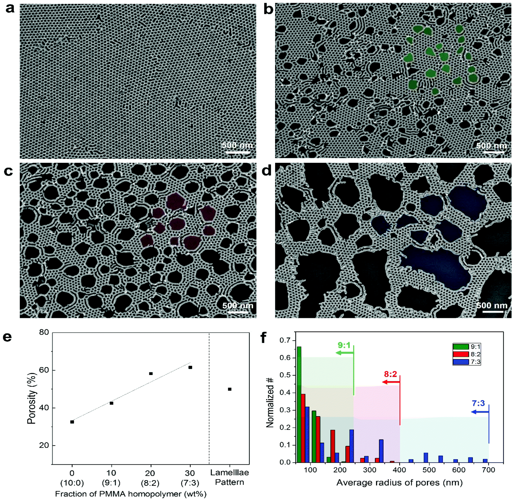 | ||
| Fig. 3 SEM images of hierarchical porous Au nanostructure pattern-transferred from bimodal self-assembled nanotemplate [(a) 10:0, (b) 9:1, (c) 8:2 and (d) 7:3]. (e) Porosity analysis of (a–d). (f) The average distance from the insulating center point to metallic collector, which was analyzed based on average radius of pores. | ||
Despite the random spatial distribution of macroscopic domains, large area uniformity and connectivity of the hierarchical self-assembled structure is noticeable, which is largely owing to the relatively narrow size distribution of homopolymer domains.12,48 It is also a considerable factor for high performance optoelectronic devices, as well as well-balanced conductance and transparency, as it may offer uniform injection or extraction of charge carriers from underlaid or overlaid active semiconductor layers.49–53 The average radius of homopolymer domains at each blend composition is plotted in Fig. 3f. It can be interpreted that conductive pathway is confirmed to exist within ∼250, ∼400, and ∼700 nm from an arbitrary insulating point for 9:1, 8:2, and 7:3 blends, respectively, in average. It is noteworthy that, according to the desired applications, the average spacing between conductive pathways could be more precisely tuned by processing parameters, such as solvent annealing time or solvent vapor pressure.33 This clearly contrasts to the conventional metal grid electrodes that generally consist of alternative grids and spaces with regular pattern periods predetermined by lithographic mask structure, which typically belongs to several tens of micrometer scale.
Optoelectronic properties of hierarchical metallic nanostructures were characterized, as shown in Fig. 4. Fig. 4a presents a bare eye observation of metal nanostructures. The hierarchical porous samples made from bimodal self-assembled nanotemplates showed high levels of optical transparency largely owing to the reduced coverage of metallic film in the macrophase-separated PS homopolymer area. It is well-known that visible light is strongly reflected at a metal surface and the rest of the propagating portion undergoes an exponential decay of intensity in metallic volume. The metallic films fabricated from pristine BCP film without homopolymer showed a weak reddish color. Quantitatively, the transmittance of simple nanoporous metallic film obtained from pristine BCP decreases to 65.8% at 400 nm due to an interband transition of Au. This contrasts to bimodal porous films prepared from 8:2 and 7:3 blends, which show an optical transmittance above 73%, 80% over the entire visible range and 80.7%, 85.7% at 550 nm, respectively (Fig. 4b). Notably, the electrical resistances of bimodal porous films (33.4 Ω □−1 for 8:2 blends & 41.6 Ω □−1 for 7:3 blends) are not significantly lower than that of simple nanoporous one obtained from pristine BCP template (20.8 Ω □−1).
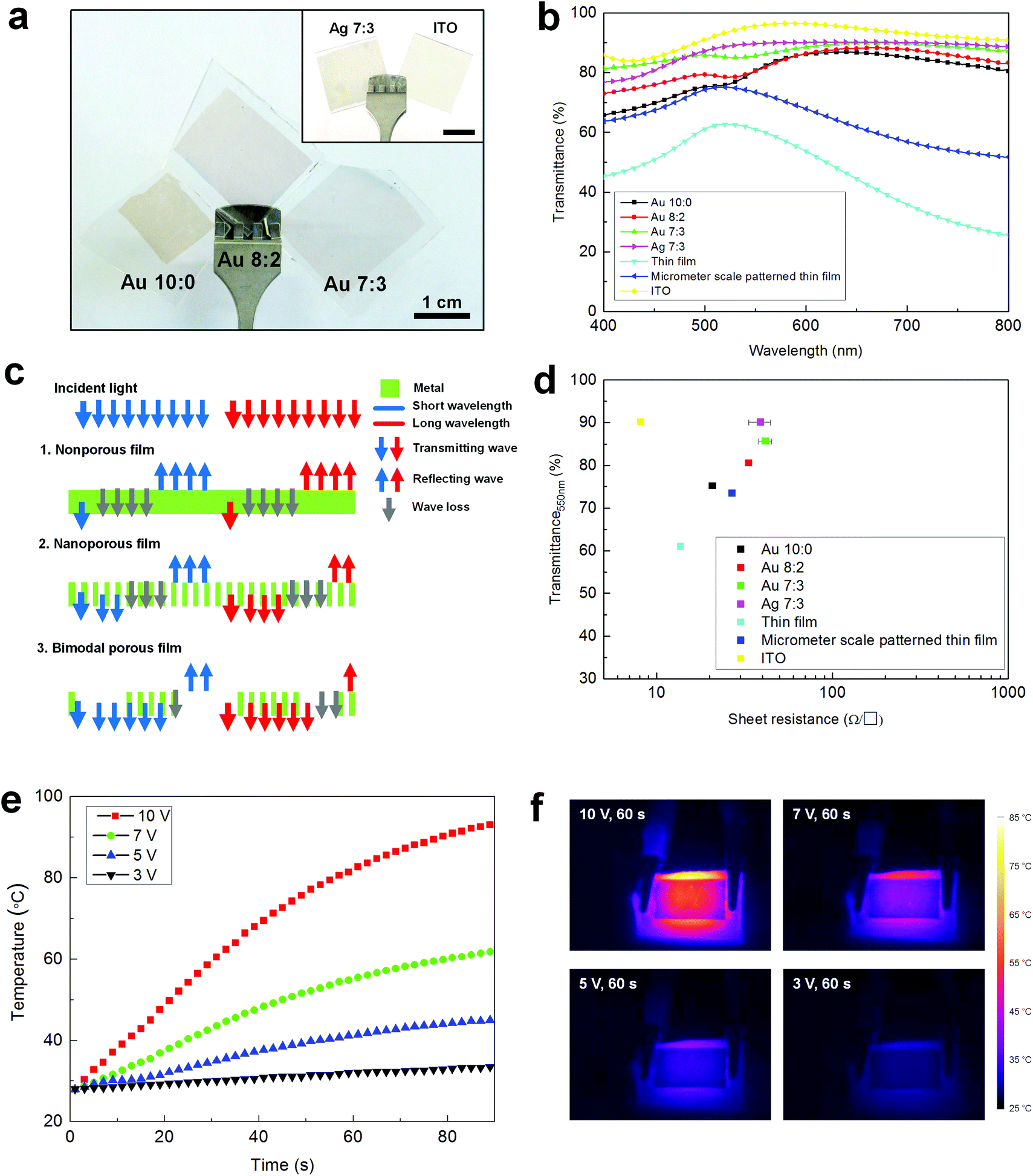 | ||
| Fig. 4 (a) Photographic image and (b) transmittance of hierarchical porous transparent electrode from bimodal phase separated BCP thin film. (c) Schematic illustration of transmittance enhancement by bimodal porosity. (d) Plot of sheet resistance and transmittance at 550 nm. (e) Measured temperature of bimodal transparent electrode as a function of heating time and (f) infrared camera image at each input voltage. | ||
These results are even more remarkable when compared to the results for nonporous film and micrometer scale patterned thin film with a porosity of 34.9% (no nanoscale pattern) fabricated from macrophase-separated homopolymer blend films of PS and PMMA (blending ratio 7:3) (Fig. S8, ESI†). In those cases, the electrical resistance maintains a similar order of magnitude with those of nanopatterned films (13.7 Ω □−1 and 26.9 Ω □−1), but the optical transparency is significantly lower to be 61.1% and 73.5% at 550 nm, respectively. In particular, the transmittance results in a long wavelength regime confirm the optical effect from nanoscale patterning. When nanoporous film from pristine BCP and micrometer scale patterned film having similar porosities (32.5% & 34.9%) are compared, the difference of optical transmittance in the short wavelength regime below ∼500 nm is not significant due to the intrinsic absorption determined by the total amount of metallic material. In the long wavelength regime, by contrast, transmittance of nanoporous film was dramatically enhanced compared to micrometer scale patterned film; for example, by 28.1% at 700 nm, due to the significant suppression of light reflection induced by the tens of nanometer scale nanoporous structure. This nanonetwork, much smaller than visible wavelength, can be regarded as diluted metal film with weakened intrinsic metallic properties according to homogenization theory,30 and thus the light reflection from this nanoporous film could be significantly suppressed. To this nanoporous film, additionally formed microscale pores further improve the optical transparency in the short wavelength regime. These two distinctive mechanisms for the enhancement of optical transmittance are schematically illustrated in Fig. 4c. Based on this optical principle, Ag with relatively low optical loss in the visible range was utilized to form a bimodal porous transparent electrode. As shown in Fig. 4a inset and 4b, a high transparency of 90.1% at 550 nm was realized for 7:3 blends, showing the electrical resistance of 39.0 Ω □−1. For comparison with other materials, the absorption coefficient of our self-assembled transparent electrode is evaluated with regard to practical and effective thickness, respectively (Table S1, ESI†) and it is confirmed that the bimodal porosity significantly lowers the absorption coefficient.54
Fig. 4d compares the optoelectronic properties of TCEs with different patterned morphologies. The desirable effect from hierarchical porosity was confirmed again by preventing the strong reflection at a metal surface a well as the exponential decay of light intensity in a highly glossy metal. It is evident how to judiciously design the porous structure of metallic film for a high level of optical transparency well-balanced with high electrical conductance. Our bimodal self-assembled transparent conductor attains competitive optoelectronic properties along with evenly distributed, highly dense conducting pathways in random orientation, which evidently contrasts to previous reports for metal grid-type TCEs (Table S2, ESI†).14,15 These macroscopic and nanoscale pores could synergistically contribute overall to decrease the optical loss, particularly intrinsic absorption of material in the short wavelength regime and suppress light reflection from the metal surface in the long wavelength regime, respectively. It is noteworthy that while only a simple single elemental metal nanomesh is demonstrated in this work as a model system, metallic alloys or other topological modification such as layered, core–shell structures would be applicable for a broad range of functionalities such as work function tunability, antireflection for high transmittance, and enhanced conductance from this bimodal phase separated template.
As an immediate application of our bimodal transparent electrode, a transparent Joule heater was tested. Constant DC voltage was applied between the two side ends of the electrodes. The Au electrode with an optical transparency of 80.7% (550 nm) and electric resistance of 33.4 Ω □−1 showed a rapid response of temperature increase, reaching the 55 and 82 °C within 1 min and showing steady-state temperatures of 61 and 93 °C, at the applied input voltages of 7 and 10 V, respectively (Fig. 4e and f). Considering conductance of our transparent electrode, the response time and steady-state temperature, which are highly related with power dissipation, are quite reasonable compared with reports of Kim et al.55 where Ag nanowire films with ∼10 Ω □−1 and 50 Ω □−1 could reach 70 °C at an input voltage of 5 V and 12 V within ∼100 seconds and of Kang et al.56 where doped graphene with ∼43 Ω □−1 could reach 100 °C at an input voltage of 12 V within 100 seconds. It is noteworthy that the well-distributed metallic conductive pathways replicated from bimodal self-assembled templates might contribute to uniform, large area heating. This reliable heating behavior of our hierarchical metal conductor would be useful for anti-fog, anti-icing, and so on.55–58
Conclusions
In summary, we demonstrated bimodal macro- and micro-phase separated BCP thin films for hierarchical porous metal nanomesh TCEs. Homopolymers with high molecular weights were blended with BCPs and the macrophase separation of homopolymers decoupled from nanoscale microphase separation BCP was confirmed under solvent annealing conditions. Along with nanoscale porosity from BCP, the homopolymer rich regions could be utilized as large vacancies for enhanced visible light penetration upon the subsequent pattern transfer into metallic thin films. Using this strategy, the hierarchical porous TCEs with reasonable optoelectronic properties was realized with highly dense conductive pathways, which could be applied as a uniform transparent heater. Motivated from this work, we expect many different homopolymers with interesting functionalities could be similarly incorporated in BCP self-assembly, where novel functional nanostructures might be achievable for a wide range of applications including optoelectronics, energy conversion device, and membrane.Experimental
Formation of bimodal phase separated BCP nanotemplate
For the perpendicular orientation of BCP, the surface energy of substrate was modified with a PS-r-PMMA random copolymer brush with hydroxyl functional groups.59 In detail, the PS-r-PMMA brush solution (solvent: toluene) with 1 wt% was spin-cast on UV ozone-treated substrate over 20 min, and then for the covalent bonding between the functional group of substrate and PS-r-PMMA brush, the thermal annealing at 150 °C was performed over 1 hour in vacuum. Then, after the unreacted brush molecules were thoroughly washed with toluene, a blending solution of PS-b-PMMA and homopolymer (PS or PMMA) in toluene with a proper weight ratio was spin-cast and THF solvent annealing was performed for bimodal self-assembly. The molecular weight of PS-b-PMMA was properly selected for desired morphologies among 105 kg mol−1-b-106 kg mol−1, 140 kg mol−1-b-65 kg mol−1, 62 kg mol−1-b-143 kg mol−1, and so on. Similarly, the PS or PMMA homopolymer was selected among 50 kg mol−1, 230 kg mol−1, 400 kg mol−1, and 900 kg mol−1. The chamber for solvent annealing was a hand-made, cylinder-type with dimensions of 15 cm radius and 12 cm height. The added amount of THF was roughly 1 mL and solvent annealing time was controlled in the range of 1–2 hours.Pattern transfer into metallic nanostructure
To fabricate the electric-conducting film, the pattern transfer process of polymeric BCP nanotemplate into metallic component was performed using conventional deposition and lift-off. At first, the PMMA domain in PS-b-PMMA nanotemplate was selectively etched out through reactive ion etching (RIE) or acetic acid & water treatment. The O2/Ar plasma was used for dry etching of RIE and wet etching of diluted acetic acid solution & water treatment was performed during 10 min at each step. To avoid the pattern collapse, the RIE process was preferred to lamellar- and PS cylinder-forming BCP. After complete etching of PMMA, thermal evaporation of gold proceeded to form the hierarchical porous metallic network. The deposition rate was roughly 0.5 nm s−1 and the height of deposited material was 15–20 nm.Measurements
Nanoscale morphologies from diverse bimodal self-assembled nanotemplates were measured by scanning electron microscopy (SEM) (Hitachi S-4800). For the image analysis of SEM, freely available software ImageJ was utilized. For the optical property measurement, commercially available ultraviolet-vis spectroscopy (UV-2600, SHIMADZU) was used. The electric resistance was measured by 4-point probe sheet resistance measuring system (CMT-SR2000N, Advanced Instrument Technology).Author contributions
J.Y.K. and H.M.J. contributed equally to this work. S.O.K. and J.S. supervised the project. J.Y.K., H.M.J., S.O.K., J.S., T.C., S.J., B.H.K., D.O.S., Y.L. and K.M.K. discussed and wrote the manuscript. J.Y.K. and H.M.J. proposed the initial idea of this project. J.Y.K. was responsible for the entire experimental process and analysis and J.Y.K., H.M.J., S.K.C., J.S.K., J.Y.C., J.H.K., G.G.Y. and S.J. conducted the sample fabrications and characterizations. All authors have given approval to the final version of the manuscript.Conflicts of interest
There are no conflicts to declare.Acknowledgements
This work was financially supported by the Multi-Dimensional Directed Nanoscale Assembly Creative Research Initiative (CRI) Center (2015R1A3A2033061), the International Collaborative Energy Technology R&D Program of the Korea Institute of Energy Technology Evaluation and Planning (KETEP), granted financial resource from the Ministry of Trade, Industry & Energy, Republic of Korea (20158510050020) and NRF grants funded by the MSIP (2013 M3C1A3063598).References
- T. Minami, Semicond. Sci. Technol., 2005, 20, S35–S44 CrossRef CAS.
- G. Eda, G. Fanchini and M. Chhowalla, Nat. Nanotechnol., 2008, 3, 270–274 CrossRef CAS PubMed.
- X. Wang, L. Zhi and K. Müllen, Nano Lett., 2008, 8, 323–327 CrossRef CAS PubMed.
- K. S. Kim, Y. Zhao, H. Jang, S. Y. Lee, J. M. Kim, K. S. Kim, J. H. Ahn, P. Kim, J. Y. Choi and B. H. Hong, Nature, 2009, 457, 706–710 CrossRef CAS PubMed.
- P. B. Catrysse and S. Fan, Nano Lett., 2010, 10, 2944–2949 CrossRef CAS PubMed.
- D. S. Hecht, L. Hu and G. Irvin, Adv. Mater., 2011, 23, 1482–1513 CrossRef CAS PubMed.
- H. Kang, S. Jung, S. Jeong, G. Kim and K. Lee, Nat. Commun., 2015, 6, 6503 CrossRef CAS PubMed.
- K. Ellmer, Nat. Photonics, 2012, 6, 809–817 CrossRef CAS.
- J. Y. Lee, S. T. Connor, Y. Cui and P. Peumans, Nano Lett., 2008, 8, 689–692 CrossRef CAS PubMed.
- L. Hu, H. S. Kim, J.-Y. Lee, P. Peumans and Y. Cui, ACS Nano, 2010, 4, 2955–2963 CrossRef CAS PubMed.
- E. C. Garnett, W. Cai, J. J. Cha, F. Mahmood, S. T. Connor, M. Greyson Christoforo, Y. Cui, M. D. McGehee and M. L. Brongersma, Nat. Mater., 2012, 11, 241–249 CrossRef CAS PubMed.
- T. Gao, B. Wang, B. Ding, J.-K. Lee and P. W. Leu, Nano Lett., 2014, 14, 2105–2110 CrossRef CAS PubMed.
- D. S. Ghosh, T. L. Chen and V. Pruneri, Appl. Phys. Lett., 2010, 96, 041109 CrossRef.
- S. Hong, J. Yeo, G. Kim, D. Kim, H. Lee, J. Kwon, H. Lee, P. Lee and S. H. Ko, ACS Nano, 2013, 7, 5024–5031 CrossRef CAS PubMed.
- J. H. Park, D. Y. Lee, Y.-H. Kim, J. K. Kim, J. H. Lee, J. H. Park, T.-W. Lee and J. H. Cho, ACS Appl. Mater. Interfaces, 2014, 6, 12380–12387 CAS.
- M. Park, C. Harrison, P. M. Chaikin, R. A. Register and D. H. Adamson, Science, 1997, 276, 1401–1404 CrossRef CAS.
- S. O. Kim, H. H. Solak, M. P. Stoykovich, N. J. Ferrier, J. J. de Pablo and P. F. Nealey, Nature, 2003, 424, 411–414 CrossRef CAS PubMed.
- R. Ruiz, H. Kang, F. A. Detcheverry, E. Dobisz, D. S. Kercher, T. R. Albrecht, J. J. de Pablo and P. F. Nealey, Science, 2008, 321, 936–939 CrossRef CAS PubMed.
- K. G. A. Tavakkoli, K. W. Gotrik, A. F. Hannon, A. Alexander-Katz, C. A. Ross and K. K. Berggren, Science, 2012, 336, 1294–1298 CrossRef CAS PubMed.
- B. H. Kim, S. J. Park, H. M. Jin, J. Y. Kim, S.-W. Son, M.-H. Kim, C. M. Koo, J. Shin, J. U. Kim and S. O. Kim, Nano Lett., 2015, 15, 1190–1196 CrossRef CAS PubMed.
- J. Y. Kim, J. Lim, H. M. Jin, B. H. Kim, S.-J. Jeong, D. S. Choi, D. J. Li and S. O. Kim, Adv. Mater., 2016, 28, 1591–1596 CrossRef CAS PubMed.
- H. M. Jin, S. H. Lee, J. Y. Kim, S.-W. Son, B. H. Kim, H. K. Lee, J. H. Mun, S. K. Cha, J. S. Kim, P. F. Nealey, K. J. Lee and S. O. Kim, ACS Nano, 2016, 10, 3435–3442 CrossRef CAS PubMed.
- T. Thurn-Albrecht, J. Schotter, G. A. Kästle, N. Emley, T. Shibauchi, L. Krusin-Elbaum, K. Guarini, C. T. Black, M. T. Tuominen and T. P. Russell, Science, 2000, 290, 2126–2129 CrossRef CAS PubMed.
- Q. Peng, Y.-C. Tseng, S. B. Darling and J. W. Elam, ACS Nano, 2011, 5, 4600–4606 CrossRef CAS PubMed.
- W. A. Lopes and H. M. Jaeger, Nature, 2001, 414, 735–738 CrossRef CAS PubMed.
- C. K. Jeong, H. M. Jin, J.-H. Ahn, T. J. Park, H. G. Yoo, M. Koo, Y.-K. Choi, S. O. Kim and K. J. Lee, Small, 2014, 10, 337–343 CrossRef CAS PubMed.
- C. Cummins, T. Ghoshal, J. D. Holmes and M. A. Morris, Adv. Mater., 2016, 28, 5586–5618 CrossRef CAS PubMed.
- J. A. Dolan, B. D. Wilts, S. Vignolini, J. J. Baumberg, U. Steiner and T. D. Wilkinson, Adv. Opt. Mater., 2015, 3, 12–32 CrossRef CAS.
- A. Rahman, A. Ashraf, H. Xin, X. Tong, P. Sutter, M. D. Eisaman and C. T. Black, Nat. Commun., 2015, 6, 5963 CrossRef CAS PubMed.
- J. Y. Kim, H. Kim, B. H. Kim, T. Chang, J. Lim, H. M. Jin, J. H. Mun, Y. J. Choi, K. Chung, J. Shin, S. Fan and S. O. Kim, Nat. Commun., 2016, 7, 12911 CrossRef PubMed.
- J. A. Dolan, M. Saba, R. Dehmel, I. Gunkel, Y. Gu, U. Wiesner, O. Hess, T. D. Wilkinson, J. J. Baumberg, U. Steiner and B. D. Wilts, ACS Photonics, 2016, 3, 1888–1896 CrossRef CAS PubMed.
- H. Park, J.-U. Kim and S. Park, Nanoscale, 2012, 4, 1362–1367 RSC.
- P. C. Millett, Comput. Mater. Sci., 2016, 125, 20–27 CrossRef CAS.
- P. Mansky, Y. Liu, E. Huang, T. P. Russell and C. J. Hawker, Science, 1997, 275, 1458–1460 CrossRef CAS.
- D. Y. Ryu, K. Shin, E. Drockenmuller, C. J. Hawker and T. P. Russell, Science, 2005, 308, 236–239 CrossRef CAS PubMed.
- E. Kim, H. Ahn, S. Park, H. Lee, M. Lee, S. Lee, T. Kim, E.-A. Kwak, J. H. Lee, X. Lei, J. Huh, J. Bang, B. Lee and D. Y. Ryu, ACS Nano, 2013, 7, 1952–1960 CrossRef CAS PubMed.
- E. Han, K. O. Stuen, Y.-H. La, P. F. Nealey and P. Gopalan, Macromolecules, 2008, 41, 9090–9097 CrossRef CAS.
- Y. Liu, G. Reiter, K. Kunz and M. Stamm, Macromolecules, 1993, 26, 2134–2136 CrossRef CAS.
- M. Appel and G. Fleischer, Macromolecules, 1993, 26, 5520–5525 CrossRef CAS.
- T. P. Russell, R. P. Hjelm and P. A. Seeger, Macromolecules, 1990, 23, 890–893 CrossRef CAS.
- M. D. Whitmore and J. Noolandi, Macromolecules, 1985, 18, 2486–2497 CrossRef CAS.
- X. Quan, I. Gancarz, J. T. Koberstein and G. D. Wignall, Macromolecules, 1987, 20, 1431–1434 CrossRef CAS.
- M. W. Matsen, Macromolecules, 1995, 28, 5765–5773 CrossRef CAS.
- L. D. Williamson and P. F. Nealey, Macromolecules, 2015, 48, 3997–4003 CrossRef CAS.
- I. P. Campbell, G. J. Lau, J. L. Feaver and M. P. Stoykovich, Macromolecules, 2012, 45, 1587–1594 CrossRef CAS.
- J. Y. Kim, B. H. Kim, J. O. Hwang, S.-J. Jeong, D. O. Shin, J. H. Mun, Y. J. Choi, H. M. Jin and S. O. Kim, Adv. Mater., 2013, 25, 1331–1335 CrossRef CAS PubMed.
- K. M. Diederichsen, R. R. Brow and M. P. Stoykovich, ACS Nano, 2015, 9, 2465–2476 CrossRef CAS PubMed.
- F. Afshinmanesh, A. G. Curto, K. M. Milaninia, N. F. van Hulst and M. L. Brongersma, Nano Lett., 2014, 14, 5068–5074 CrossRef CAS PubMed.
- Y. Zhu, Z. Sun, Z. Yan, Z. Jin and J. M. Tour, ACS Nano, 2011, 5, 6472–6479 CrossRef CAS PubMed.
- M.-S. Lee, K. Lee, S.-Y. Kim, H. Lee, J. Park, K.-H. Choi, H.-K. Kim, D.-G. Kim, D.-Y. Lee, S. Nam and J.-U. Park, Nano Lett., 2013, 13, 2814–2821 CrossRef CAS PubMed.
- H.-G. Im, S. Jeong, J. Jin, J. Lee, D.-Y. Youn, W.-T. Koo, S.-B. Kang, H.-J. Kim, J. Jang, D. Lee, H.-K. Kim, I.-D. Kim, J.-Y. Lee and B.-S. Bae, NPG Asia Mater., 2016, 8, e282 CrossRef CAS.
- B. Han, K. Pei, Y. Huang, X. Zhang, Q. Rong, Q. Lin, Y. Guo, T. Sun, C. Guo, D. Carnahan, M. Giersig, Y. Wang, J. Gao, Z. Ren and K. Kempa, Adv. Mater., 2014, 26, 873–877 CrossRef CAS PubMed.
- S. Wu, L. Li, H. Xue, K. Liu, Q. Fan, G. Bai and J. Wang, ACS Nano, 2017, 11, 9898–9905 CrossRef CAS PubMed.
- R. Das Suprem, S. Sadeque, C. Jeong, R. Chen, A. Alam Muhammad and B. Janes David, Nanophotonics, 2016, 5, 180 Search PubMed.
- T. Kim, Y. W. Kim, H. S. Lee, H. Kim, W. S. Yang and K. S. Suh, Adv. Funct. Mater., 2013, 23, 1250–1255 CrossRef CAS.
- J. Kang, H. Kim, K. S. Kim, S.-K. Lee, S. Bae, J.-H. Ahn, Y.-J. Kim, J.-B. Choi and B. H. Hong, Nano Lett., 2011, 11, 5154–5158 CrossRef CAS PubMed.
- D. Sui, Y. Huang, L. Huang, J. Liang, Y. Ma and Y. Chen, Small, 2011, 7, 3186–3192 CrossRef CAS PubMed.
- T. Sannicolo, M. Lagrange, A. Cabos, C. Celle, J.-P. Simonato and D. Bellet, Small, 2016, 12, 6052–6075 CrossRef CAS PubMed.
- S.-J. Jeong, G. Xia, B. H. Kim, D. O. Shin, S.-H. Kwon, S.-W. Kang and S. O. Kim, Adv. Mater., 2008, 20, 1898–1904 CrossRef CAS.
Footnotes |
| † Electronic supplementary information (ESI) available: Additional SEM images and analysis, summary table for transparent electrode researches. See DOI: 10.1039/c7nr07178g |
| ‡ These authors contributed equally. |
| This journal is © The Royal Society of Chemistry 2018 |