
Recent progresses and challenges in colloidal quantum dot light-emitting diodes: a focus on electron transport layers with metal oxide nanoparticles and organic semiconductors
Jaehoon
Kim

Department of Electronic Engineering, Gachon University, Seongnam-si, Gyeonggi-do 13120, Republic of Korea. E-mail: jaehoonkim@gachon.ac.kr
First published on 25th September 2024
Abstract
Colloidal quantum dots (QDs) are highly promising for display technologies due to their distinctive optical characteristics, such as tunable emission wavelengths, narrow emission spectra, and superb photoluminescence quantum yields. Over the last decade, both academic and industrial research have substantially advanced quantum dot light-emitting diode (QLED) technology, primarily through the development of higher-quality QDs and more refined device structures. A key element of these advancements includes progress in the electron transport layer (ETL) technology, with metal oxide (MO) nanoparticles (NPs) like ZnO and ZnMgO emerging as superior choices due to their robust performance. Nevertheless, scalability challenges, such as particle agglomeration and positive aging, have prompted research into organic semiconductors that match the performance of MO NPs. This review aims to provide a detailed examination and comprehensive understanding of recent advances and challenges in ETLs based on both MO NPs and organic semiconductors, guiding future commercialization efforts for QLEDs.
 Jaehoon Kim | Jaehoon Kim received his BS degree in 2013 from the School of Electrical and Electronic Engineering, Yonsei University, Seoul, Korea, and his PhD degree in 2018 from the Department of Electrical and Computer Engineering, Seoul National University, Seoul, Korea. After working as a staff engineer at Samsung Display from 2018 to 2020, he joined Los Alamos National Laboratory, Los Alamos, NM, United States, as a postdoctoral research associate from 2021 to 2022. He served as an assistant professor at Dong-A University, Busan, Korea, from 2022 to 2024. In 2024, he joined the Department of Electronic Engineering at Gachon University, where he is currently an assistant professor. His research interests include organic and quantum dot optoelectronic devices and physics. |
1. Introduction
Quantum dot light-emitting diodes (QLEDs) represent a transformative advancement in display technology, heralding a new era of visual representation characterized by unparalleled color accuracy,1 efficiency,2,3 brightness,4 and scalability.5 Positioned as potential successors to organic light-emitting diodes (OLEDs),6 QLEDs utilize colloidal quantum dots (QDs) to generate pure and vibrant colors, customizable based on their nanoscale geometry.7 This distinctive feature allows QLEDs to cover a broader spectrum of the Rec. 2020 color space,1 making them invaluable for applications requiring high color fidelity, such as high-definition televisions,8 smartphones,9 and advanced computing devices.10 Besides, the QD emissive layer (EML) consists of inorganic materials, which provide enhanced durability and longer lifetime.11 This longevity, combined with potential for higher brightness levels, makes QLEDs particularly suitable for a wide range of applications. Another critical attribute of QLEDs is their efficiency; they operate at lower power levels while maintaining high luminance,3,4 especially expected to be beneficial for digital signage and television displays.12 Additionally, the manufacturing process of QLEDs offers significant benefits because they can be produced with simpler architectures,13 which require fewer processing steps. This advantage not only reduces production costs but also scales effectively to larger substrates,14 facilitating the production of larger screens or high-volume outputs without significant cost increases.15However, the performance of QLEDs is inherently linked to their electron transport layer (ETL). The efficiency,16 stability,17 and processability18 of QLEDs depend heavily on the effectiveness of this layer. Historically, the development of QLEDs has been closely linked to advancements in electron transport materials (ETMs), with metal oxide (MO) nanoparticles (NPs), such as ZnO and ZnMgO, initially preferred for their excellent performance.19,20 However, recent research in ETMs has expanded toward organic materials that offer comparable performance to MO NPs.21–24 In brief, organic ETMs have already been successfully commercialized in the field of OLEDs since the progress of QLED technology has also been significantly influenced by the evolution of ETL technology.25 Thus, as researchers continue to investigate new materials and methods for QLEDs, the focus has increasingly been on identifying more efficient ETL candidates (Fig. 1), highlighting their critical role in advancing display technologies. This ongoing interplay between materials science and device engineering drives the continuous development of cutting-edge QLEDs.
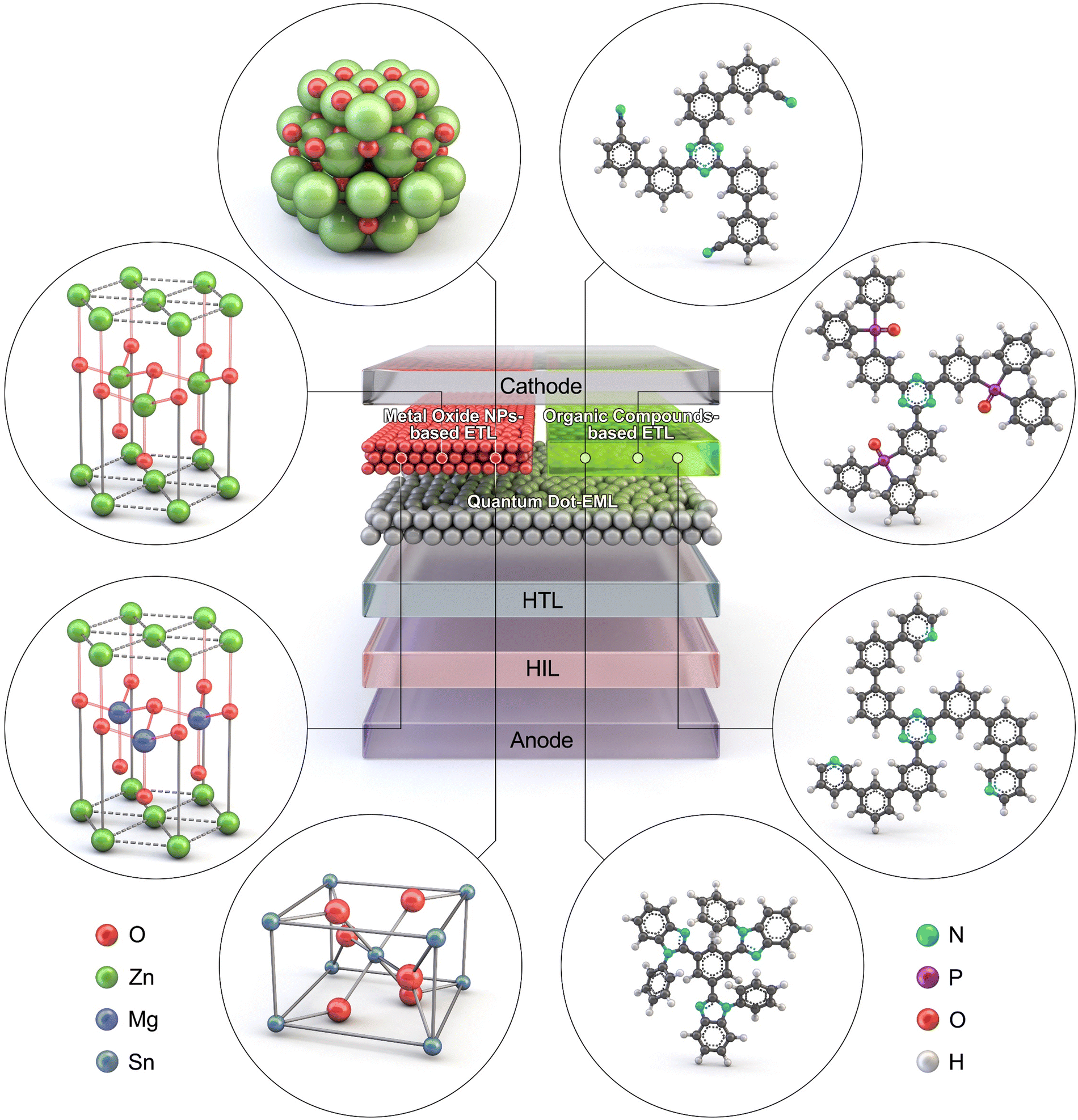 | ||
| Fig. 1 Schematic illustration of a QLED featuring ETLs based on MO NPs (ZnO, ZnMgO, SnO2) and organic semiconductors (CNT2T, PO-T2T, TmPPPyTz, TPBi). | ||
2. Significance of electron transport layer
Developing efficient and high-performance QLEDs necessitates addressing several critical challenges related to ETLs, including balanced charge injection,26 defect-free surfaces,27 and ease of processability.28 Achieving balanced electron and hole injection is vital for high-performance QLEDs, which depend on suitable charge mobility, carrier concentration, electron/hole recombination rates, electric field profiles, space-charge distribution, and energy level alignment.29 Specifically, proper energy level alignment is crucial because significant differences in the lowest unoccupied molecular orbital (LUMO) or conduction band minimum (CBM) values can impede carrier injection. Optimizing these barriers can substantially enhance the brightness and external quantum efficiency (EQE) of QLEDs.30 The trends in EQE and T50 lifetime (the time required for luminance to drop to 50% of its initial value) over the past development period, categorized by Cd-based/Cd-free QDs and MO/organic ETLs, are discussed throughout the manuscript and illustrated in Fig. 2. | ||
| Fig. 2 EQEs and T50 development progresses of QLEDs featuring various ETLs on the basis of (a) and (b) Cd-based and (c) and (d) with Cd-free QDs. | ||
MO NPs, particularly ZnO and ZnMgO NPs, are the most widely adopted ETMs for QLEDs due to their favorable chemical properties.31,32 Their high electron mobility facilitates efficient electron transport to the EML, reducing energy loss and enhancing electroluminescence (EL) efficiency. This high mobility is attributed to their crystalline structure, which minimizes barriers to electron movement.33 Furthermore, a recent study by a prominent research group demonstrated that initial electron injection creates a negatively charged intermediate state in QDs, enhancing Coulomb interactions and boosting hole injection while preventing electron over-injection.34 This sensitivity to electron injection capability underscores the significant impact of ETLs on QLED performance. ZnO and ZnMgO NPs also possess a wide band gap, which not only offers transparency in the visible spectrum and maintains optical clarity in displays but also provides a high offset relative to the CBM of the QDs.35 This ensures strong electron confinement within the QD layer, preventing leakage and enhancing recombination efficiency, thereby improving luminance and color saturation. Additionally, the synthesis of these NPs can be precisely controlled, allowing for the fine-tuning of ETL properties such as particle size and doping level.36,37
These MO NPs are not only pivotal as ETMs in QLEDs but also exhibit superior performance in other optoelectronic devices such as colloidal quantum dot photovoltaics (c-QDPVs)38 and colloidal quantum dot laser diodes (c-QLDs).39–43 Specifically, for c-QLDs, materials like ZnO or ZnMgO have been identified as suitable MO ETLs due to their nearly ideal characteristics for charge balance and electron injection at high current densities, as reported in various studies.41,42 However, in the case of NP forms of MO ETLs, their high surface-to-volume ratio can contribute to a non-ideal surface nature in c-QLDs, where a high quantum yield is critical. This has led to the adoption of sol–gel processed MO ETLs in recent devices like electrically pumped amplified spontaneous emission (ASE) diodes.42 Moreover, the high refractive indices of MO ETMs can create a suboptimal optical field profile in standard QLED architectures, peaking not within the QD part but rather at the interface between the ZnO and indium tin oxide (ITO) layers.43 To counter this, a former study has excluded MO ETL entirely, utilizing low-refractive index ITO as both the electrode and ETL, thereby achieving optically excited lasing from fully functional high-current density EL devices with an integrated optical resonator.43 Nevertheless, for electrical pumping applications, the efficient injection of electrons remains crucial, and it is reaffirmed that MO ETL is an indispensable component in c-QDLs.42
Returning to the main topic, although MO NPs have been the predominant choice for ETLs in QLEDs, there is a growing interest in organic ETLs21–24 due to inherent limitations in MO NPs. The high surface-to-volume ratio of MO NPs results in numerous surface defects,44 leading to issues such as positive aging,45 which compromise the performance and reliability of QLEDs. Additionally, these NPs suffer from colloidal instability, which poses significant challenges for processes such as inkjet printing because of their tendency to agglomerate, clog nozzles and hinder scalability for mass production.46–50 Nonetheless, historically, QLEDs utilizing organic ETLs have exhibited lower performance metrics compared to those using MO NPs, as illustrated in Fig. 2. However, this scenario is evolving as research into organic ETLs for QLEDs expands, driven by the unique benefits of organic materials. Organic ETMs generally exhibit more stable surfaces with fewer defects,23,24 which helps mitigate issues like positive aging23 and could potentially enhance the reliability of QLEDs. Furthermore, organic ETMs have been extensively adopted in OLED production, demonstrating their scalability and commercial viability.25,51 Their established use in OLEDs suggests that integrating them into QLED manufacturing can be achieved without significant new investments in infrastructure.52 Consequently, it is increasingly important not only to focus on improving efficiency and lifetime but also on exploring research trends and future directions for ETLs from the perspective of mass production of QLEDs.
This paper reviews and discusses QLEDs with various ETL candidates, focusing on MO NPs and organic semiconductors, and particularly their advantages and limitations for commercialization, as comprehensively illustrated in Fig. 3. Section 3 provides an overview of MO ETLs, categorized into ‘3.1. Progresses in metal oxide nanoparticles,’ ‘3.2. Colloidal instability and fabrication bottlenecks,’ and ‘3.3. Surface defects and positive aging’. In Section 4, hybrid configurations that utilize both MO NPs and organic ETMs are reviewed under ‘4.1. Bilayer configurations’ and ‘4.2. Mixed configurations’. Section 5 examines organic ETMs solely adopted as ETLs for QLEDs, with particular attention to ‘5.1. Electron mobility and interfacial emission,’ ‘5.2. Intrinsic instability,’ and ‘5.3. Advancements in organic electron transport layers’. Finally, Section 6 presents future directions and concluding remarks.
 | ||
| Fig. 3 Comparison of MO NPs-based and organic ETLs from the perspectives of (a) energy band diagrams and (b) and (c) electron mobility. Schematic illustrations of the distinctive properties of (d) MO NPs-based and (e) organic ETLs. | ||
3. Metal oxide nanoparticles-based electron transport layer
Synthesis of MO NPs via solution precipitation is the most widely accepted method in the field of QLEDs.53 Known for its simplicity and cost-effectiveness, this method involves the chemical precipitation of metal ions from a homogeneous solution to form MO NPs under controlled conditions. The core principle relies on the solubility dynamics of metal salts in aqueous and non-aqueous solvents. Typically, metal salts are dissolved in a suitable solvent, and a precipitating agent is added to adjust the pH or ionic strength, leading to the formation of metal hydroxides or oxides. One significant advantage of this method is its ability to produce NPs with uniform size distribution and controlled morphology by adjusting parameters such as temperature, pH, concentration, and reaction time.54 For example, lower temperatures can result in smaller particle sizes due to the reduced kinetic energy, which limits atom movement and growth.55 Similarly, the pH of the solution critically influences the nucleation and growth phases of the NPs.56 Adjusting the acidic or basic conditions can optimize the characteristics of the resulting MO NPs. The versatility of the solution precipitation method also allows for the doping of MO NPs with other elements to modify their electrical and optical properties, thereby enhancing their suitability for specific ETL applications.57–59 Overall, the solution precipitation method is notable for its operational ease, scalability, and broad applicability in creating various MO NPs such as ZnO,56 TiO2,60 and SnO2,61 which play distinct roles in ETLs. This method enables researchers and engineers to efficiently tailor the NP properties to meet specific ETL requirements.3.1. Progresses in metal oxide nanoparticles
Since then, extensive research and development have been conducted on ZnO NPs as ETLs for QLEDs. Holloway et al. were the first to report devices with an EQE exceeding 1% (red 1.7%, green 1.8%, and blue 0.22%).53 They also provided the first report on the operational lifetime of the devices over time. Notably, compared to organic ETLs such as tris(8-hydroxyquinoline)aluminum(III) (Alq3), ZnO exhibited a significantly lower turn-on voltage (Von) of 2.0 V and higher electron mobility of 2 × 10⁻³ cm2 V−1 s−1, facilitating better electron injection. The ZnO NPs not only reduced Von but also increased the current density compared to Alq3, indicating effective electron injection and hole blocking. While traditional organic ETLs require air-sensitive metals such as Mg,63 Ca,64 and LiF65 as electron injection layers, which negatively affect the device lifetime, ZnO allows for the direct deposition of Al, enhancing device longevity. However, they also noted that excessive electron injection leads to Auger recombination at the hole transport layer (HTL)/QD interface. Additionally, a characteristic not extensively covered in this study is the positive aging phenomenon,45 where luminance initially increases over time. This positive aging is a unique feature of ZnO NPs-based ETLs and an issue that needs to be addressed for commercialization (refer to Section 3.3).
ZnO NPs gained further attention after Lee et al. reported a ZnO NPs-based inverted structure QLED.66 While most former QLEDs utilized a conventional structure, an inverted structure with ZnO NPs as the ETL demonstrated effective electron injection. ZnO NPs offer the advantage of allowing the deposition of the QD layer without damage due to their robustness. A significant benefit of ZnO NPs in an inverted structure is their ability to support the deposition of a HTL or hole injection layer (HIL) on top of the QD layer via thermal evaporation. This process permits the use of various high-performance HTLs developed for OLEDs. The study compared different HTL/HIL combinations and identified the 4,4′-bis(N-carbazolyl)-1,1′-biphenyl (CBP)/MoO3/Al structure as optimal, a configuration still used in high-efficiency QLED research today.67
In 2013, Kazlas et al. presented an in-depth analysis of ZnO NPs, highlighting several critical features that were previously underexplored.68 The study revealed that the strong electron coupling between the QDs and ZnO NP films facilitates charge transfer. Initially, due to the significant potential difference, electrons transfer from the QDs to ZnO, resulting in QDs with a net positive charge. Upon device operation, electrons reinject into the QDs, restoring charge neutrality and balancing electrons and holes in a process termed ‘charge neutralization’. This strong electron coupling enhances charge transfer and emission stability, contributing to the high efficiency and operational lifetime of QLEDs. The study also confirmed that positive aging is linked to this restoration process. Additionally, the relative position of the recombination zone (RZ) can be altered by varying the QD thickness. In devices with thinner QD active layers, the RZ is closer to the ETL, causing holes in the QD to transfer to trap states in the ZnO mid-bandgap, leading to exciton quenching. Kelvin probe measurements further supported this finding by showing surface potential changes in ETL/QD films, suggesting that exciton quenching at the QD/ZnO interface is primarily due to charge transfer rather than energy transfer.
Current research continues to delve into the mechanisms of exciton quenching in ZnO NPs with considerable depth. In 2024, Sun et al. examined the impact of ligands on the electron transport properties of ZnO NPs.69 Employing density functional theory (DFT) and COMSOL Multiphysics simulations, they demonstrated that thiol ligands effectively passivates surface defects in ZnO, thereby decreasing electron concentration and enhancing the work function. Their findings revealed that 2-hydroxy-1-ethanethiol (HESH) significantly attenuates exciton quenching in QDs and enhances carrier injection in QLEDs compared to ethanolamine. Notably, HESH ligands facilitated the development of red-emitting QLEDs with an EQE of 23% and a T95 lifetime of over 12![[thin space (1/6-em)]](https://www.rsc.org/images/entities/char_2009.gif) 000 h at 1000 cd m−2. Moreover, various engineering strategies have been implemented to optimize performance, including the insertion of dielectric layers, such as poly(methyl methacrylate) (PMMA)19,70 or inorganic non-metallic solids like Al2O3,71 at the QD/ZnO interface. These layers serve to inhibit electron injection, promote electron/hole balance, and prevent exciton quenching due to defect states like dangling bonds or hydroxyl (–OH) groups. In addition to employing interlayers, approaches that involve blending QDs with low- or high-molecular-weight materials to passivate surface defects and alter electron mobility are being actively investigated (refer to Section 4.2).27
000 h at 1000 cd m−2. Moreover, various engineering strategies have been implemented to optimize performance, including the insertion of dielectric layers, such as poly(methyl methacrylate) (PMMA)19,70 or inorganic non-metallic solids like Al2O3,71 at the QD/ZnO interface. These layers serve to inhibit electron injection, promote electron/hole balance, and prevent exciton quenching due to defect states like dangling bonds or hydroxyl (–OH) groups. In addition to employing interlayers, approaches that involve blending QDs with low- or high-molecular-weight materials to passivate surface defects and alter electron mobility are being actively investigated (refer to Section 4.2).27
Furthermore, several studies have explored the diverse applications of ZnO, especially its excellent charge transport properties in sophisticated optical structures. In bottom-emitting structures, wide-angle interference techniques are utilized to manipulate light emission, enhancing viewing angles and maintaining color purity and intensity across various viewing positions.72 Yang et al. reported on the efficiency of bottom-emitting QLEDs, with EQEs of 12.0%, 14.5%, and 10.7% for red, green, and blue color, respectively.73 Notably, the thicknesses of the ZnO NP ETLs were varied according to the respective emission wavelengths: the blue-emitting QLED employed a 30 nm-thick ZnO layer, while the layers for green- and red-emitting QLEDs were 40 nm and 65 nm thick, respectively.
In contrast, top-emitting structure with multibeam interference prioritizes achieving high-resolution color tuning and increased brightness by superimposing multiple beams of light at varying phases, effectively controlling the spectral properties of the emitted light.2,72,74 The design of multibeam interference structures, such as second-order top-emitting QLEDs, requires intricate engineering to optimize light extraction.2,72 The employment of a high-mobility ETM, such as ZnO, is critical in these designs, where the optical path and interfaces between different layers must be meticulously engineered to facilitate optimal light outcoupling and electron transport. Additionally, ZnO provides several advantages, including excellent transparency and compatibility with other layers, rendering it a versatile choice for incorporation into complex optical structures. Chen et al. demonstrated the feasibility of adjusting the optical cavity by varying the ZnO thickness in an inverted top-emitting structure to produce both first and second order interferences.72 Importantly, ZnO NP films exhibited high mobility (approximately 1.8 × 10⁻³ cm2 V−1 s−1), which allowed for variations in thickness without adversely affecting the current–voltage (I–V) characteristics. Although not extensively covered in their study, the ability to demonstrate both first and second order interferences by adjusting the ZnO thickness highlights the significant advantages of using ZnO. Ideally, first order interference provides superior theoretical optical efficiency due to the shorter attenuation path of light within the optical medium.75,76 However, in practice, the extremely thin device structure requires first order interference to position the QD EML close to the bottom of the substrate, which might lead to potential plasmonic quenching from the metal substrate.6 Consequently, second order interference often proves more practical than first order interference for device implementation and display applications.75 Thus, the high mobility of ZnO facilitates the achievement of second order interference, offering a practical advantage in these applications.
Among various doped ZnO NPs, Al-doped ZnO (AZO) NPs demonstrate superior performance in terms of brightness, current efficiency (CE), and Von, attributable to their high electron conductivity and smooth surfaces.77 Moreover, the energy band structure of AZO NPs can be modified by adjusting the doping concentration, with photoluminescence (PL) measurements confirming that this doping reduces spontaneous electron transfer at the QD/ETL interface by lowering work functions and CBM.58 Conversely, AZO NPs with decreased electron conductivity have also been documented, exploring the impact of Al doping on carrier distribution and recombination rates within the QD EML through optoelectronic simulations.57
Similarly, Ga-doped ZnO (GZO) NPs, synthesized via a room temperature solution process without post-treatment or heavy organic ligands, present another approach for fabricating high-performance QLEDs. A previous study varied the Ga concentration in GZO NPs from 0 to 12 at%, achieving high-quality monodisperse NPs with excellent crystallinity.37 The resulting QD-LEDs demonstrated exceptional luminance levels of approximately 44000 cd m−2, and a CE of 13.1 cd A−1 at an 8% Ga doping level. These notable improvements in brightness and efficiency are attributed to the Ga dopants, which enhance electron transfer to the adjacent QD layer and reduce exciton emission quenching within the QDs.
In the context of In doping, Guo et al. developed a green-emitting InP QLED utilizing an ETL composed of In-doped ZnO (IZO) NPs.78 These IZO NPs not only reduce exciton quenching in the InP QD EML by minimizing defect states but also enhance charge balance by restricting electron injection, thereby boosting device performance. The refined InP QLED achieved a maximum EQE of 5.42% and a CE of 21.22 cd A−1, which is triple the performance of the control device that uses a standard ZnO ETL.
Ning et al. proposed a method involving Li doping in ZnO, thereby enhancing the performance of InP QLEDs.81 Li doping passivates the intrinsic defect states in ZnO NPs, increases electron mobility, reduces spontaneous charge transfer at the ZnO/QD interface, and minimizes current leakage in QLEDs. Similarly, Kim et al. explored the use of Li- and Mg-doped ZnO NPs, designated as MLZO NPs, as ETL in highly efficient and durable QLEDs.82 Co-doping ZnO with Mg and Li increases its bandgap and electrical resistivity, improving charge balance within the QD EML. Additionally, co-doping reduces the concentration of –OH groups on the oxide surface and extends the exciton decay time of the MO, enhancing overall device performance.
The CBM of ZnO NPs is also significantly influenced by Y doping levels, with the CBM adjustable from 3.55 to 2.77 eV as Y content increased from 0 to 9.6%.79 This variation in the CBM helps create a larger barrier at the cathode, improving the modulation of electron injection. By utilizing lower Y-doped (2%) ZnO, an optimal charge balance was achieved in the QLED, leading to substantial enhancements in device performance.
Doping ZnO with Sn is known to shift the CBM upward, reduce electron mobility, and decrease the number of defect sites.83 ZnSnO not only diminishes surface –OH oxygen defects on ZnO but also increases resistivity and shallows the CBM, thereby impeding excess electrons and reducing Auger recombination. Specifically, introducing Sn into ZnO results in a reduction in particle size; the average length of the Zn–O bond decreases from 2.001 to 1.985 Å, compared to 2.145 Å in Sn–O bonds.83 Consequently, ZnO and ZnSnO are more advantageous than SnO in terms of bonding, leading to smaller particle sizes. Notably, a longer bond length typically indicates weaker bonding strength, which implies a higher susceptibility to breakage. The shortened bond length and reduced particle size enhance the colloidal stability of the NPs, allowing ZnSnO ink to remain clear even after three days in air.83
(1) Shallower CBM: doping ZnO with Mg leads to a shallower CBM because the substitution of Mg2+ increases the overall bandgap. This increase is a result of the naturally larger bandgap of MgO compared to that of ZnO.85 The bandgap adjustment causes a shift in the CBM to higher energies, thereby affecting the optoelectronic properties.
(2) Lower electron conductivity: in MO semiconductors such as ZnO, oxygen vacancies (VO) typically enhance electron conductivity by providing free electron density.86–88 However, when Mg is introduced, the bond between Mg and oxygen atoms is stronger than that between Zn and oxygen atoms, reducing the likelihood of VO formation.89 This stronger bonding results in fewer free electrons and consequently reduces electron conductivity.
(3) Passivated surface defect states: Mg doping significantly enhances the stability of ZnO by reducing surface defect states such as VO89 and interstitial zinc (Zni).90 This results in surface passivation, which is advantageous for minimizing nonradiative recombination and enhancing luminescence by saturating reactive sites on the surface.44 The improvements in local electronic structure modify the band alignment and surface conductivity, thereby enhancing device performance through reduced leakage currents and improved barrier properties.
Chen et al. explored the differences between ZnO and ZnMgO, arguing that incorporating ZnMgO as an interlayer at the ZnO/QD interface in QLEDs can enhance device efficiency.91 This enhancement is due to the shallower CBM of ZnMgO by 0.33 eV and its reduced conductivity, which improves charge balance. Mg doping increases the binding energy of Mg–O to approximately 393.7 kJ mol−1, significantly higher than the 284.1 kJ mol−1 for Zn–O. This higher binding energy reduces the likelihood of oxygen escape and VO formation. The consequent reduction in VO diminishes free electron density and decreases conductivity and surface oxygen defect states, thus mitigating quenching and nonradiative decay. It has been noted that the VO passivation effect of ZnMgO is comparable to that achieved by applying a PMMA dielectric polymer layer on ZnO, which suppresses interfacial quenching by passivating defect states.92
The doping concentration of Mg in ZnMgO significantly influences its optoelectrical properties and the performance of QLED devices. Moon et al. varied the molar concentration of metal acetate hydrate in ZnMgO from 0 to 15 mol%.93 Their findings indicated that as the concentration increased from 0 to 15 mol%, the mobility of ZnMgO decreased from 2.15 × 10⁻⁴ to 0.95 × 10⁻⁵ cm2 V−1 s−1. Conversely, the bandgap widened from 3.82 eV to 3.99 eV, and the CBM shifted upwards from −3.46 to −3.41 eV. Optimal performance was observed at a 12.5 mol% doping level, while an excessive 15 mol% Mg doping led to a significant decrease in electron mobility to 0.95 × 10⁻⁵ cm2 V−1 s−1, causing an imbalance by overly reducing electron injection.
While ZnMgO substantially reduces VO compared to ZnO, it does not completely eliminate them, prompting further research to address these remaining defects. Notable methods include doping with halogen ions,94 incorporating additional dopants,82 and adding an outer shell to ZnMgO.95 An effective strategy involves the use of halogen ions such as fluoride (F−) or chloride (Cl−), which can passivate inherent VO due to their high electronegativity and ability to integrate into the lattice in place of missing oxygen. This interaction strengthens the crystal structure and enhances the semiconducting properties of ZnMgO. In a 2023 study, Wu et al. demonstrated that stirring a NaCl solution dissolved in methanol with pre-synthesized ZnMgO effectively passivates VO with Cl− ions.94 This process not only prevents exciton quenching at the QD/ZnMgO interface but also facilitates hole transport by replacing the insulating oleic acid (OA) on the QD surface with Cl− ions, thus enhancing charge injection balance. Halide ions such as Cl− deepen the CBM of ZnMgO, beneficial for InP QDs with shallow CBM by impeding electron injection and improving charge balance. This contrasts with previous research on CdSe QLEDs, where shallowing the CBM of MO ETLs was utilized to reduce electron injection.82 Additionally, reports have described enhanced stability of ZnMgO coated with an additional shell such as MgO or Mg(OH)2.95
In addition to previous treatments with halogen ions or Mg(OH)2 shells, there have been numerous reports on modifying the surface of ZnMgO using acrylate functional species, such as zinc acrylate.16 Unlike halogen ions or Mg(OH)2 shells, which primarily reduce VO states, these acrylate functional species decrease both surface VO and surface –OH defects. The –OH groups on MO surfaces are well-known electron quenchers that diminish device performance by quenching excitons and reducing electron transport characteristics.96 Moreover, the surface acrylates on ZnMgO NPs induce a dipole effect, which shifts the CBM upward, impeding electron injection and enhancing charge injection.16 While a detailed exploration of various studies is planned throughout the manuscript, it is important to summarize how the modification of MO ETL surfaces—including but not limited to ZnMgO and other MOs such as ZnO—through metal doping,77 shelling,97 and additive passivation27,98,99 can effectively alter energy levels, particularly the CBM. These modifications can either impede or accelerate electron injection. In metal doping, the introduction of dopants with varying bandgaps can change the effective bandgap, leading to shifts in the CBM.77 Similarly, shelling can cause shifts in the CBM across the entire ETL due to the differing bandgaps of the materials used in the shell.97 Notably, ligand treatment has proven to be an effective method for altering the CBM, with ligands creating surface dipole moments that can either deepen or shallow the CBM.98
However, a recent study challenged the prevailing view that exciton quenching in QD/ZnMgO films is primarily due to traps such as VO states or –OH groups.100 This research suggested that the main cause of PL quenching at the QD/ZnMgO interface is not only traps but also field-enhanced energy transfer. InP QDs, being heavily n-doped, have a Fermi energy level of about −3.88 eV. ZnMgO, with a shallow CBM of −3.48 eV, has a deeper Fermi level of −4.3 eV compared to InP QDs. This mismatch in the Fermi levels creates a diffusion potential (Vdiff) at the interface, forming a pseudo-electrical field (Efield) that accelerates electron transfer from the QD to ZnMgO. When the QDs and ZnMgO are bonded, rapid electron transfer to the ZnMgO side leads to electron accumulation, whereas holes accumulate on the QD side. These accumulated charges create an Efield that opposes the initial pseudo-Efield, effectively neutralizing it. This results in field-enhanced electron delocalization within the QD EML, increasing energy transfer between the QDs and leading to PL quenching. Therefore, this study concluded that while low bias or thin-shelled QDs exhibit quenching mainly due to traps, high bias or thick-shelled QDs exhibit quenching predominantly due to field-enhanced energy transfer. Thus, the field-enhanced energy transfer at the QD/ZnMgO interface re-emphasizes the substantial impact of the QD/MO ETL on the operational stability and reliability of QLEDs, highlighting the importance of effective interfacial engineering.
Additionally, various studies have examined the degradation mechanisms of QLEDs utilizing ZnMgO as the ETL. Commonly, the principal degradation mechanism in QLEDs involves excessive electron injection from ZnMgO (or ZnO), leading to the detachment of ligands from the QD surface.101 Moreover, this surplus of electrons can leak into the HTL, resulting in the HTL degradation. However, a former study has suggested that the intrinsic degradation of the ZnMgO ETL itself is a primary cause of deterioration in blue QLEDs.102 The study highlighted a high electron injection barrier between the blue QDs and ZnMgO, which leads to electrical stress and electron accumulation in the MO ETL, thereby inducing degradation. Contrary to the behavior in ZnMgO ETLs, Qian et al. observed different excited electron dynamics in blue QLEDs with ZnO ETLs, as evidenced by charge-modulated electro–absorption and capacitance–voltage characteristics.103 Electron migration across the type-II junction causes space-charge buildup, which increases the operating voltage and leads to a shorter lifetime for blue QLEDs due to rapid degradation at the QD/ETL interface. In contrast, the more stable red QLEDs deteriorate more gradually, primarily due to the aging of the HTL. Additional research has demonstrated that the driving voltage of ZnMgO-based electron-only devices (EODs) decreases over time due to this vulnerability, whereas EODs based on ZnO do not exhibit changes in their driving voltage over time, indicating that ZnMgO is more susceptible to electron stress than ZnO.104
Beyond surface modification and degradation mechanisms, ZnMgO has been extensively employed across various research themes, notably in enhancing the functionality of various optical structures in QLEDs due to its advantageous electron mobility and robustness.20,105,106 For instance, Zhang et al. successfully used a combination of ZnMgO and poly(3,4-ethylenedioxythiophene)polystyrene sulfonate (PEDOT:PSS) as an effective charge generation layer (CGL) in a tandem structure.20,105 The CGL serves as a critical component in tandem-structured QLEDs, facilitating charge injection and recombination across multiple emissive units. Additionally, it effectively divides the device into separate subcells, each capable of independent emission, which enhances the overall efficiency and brightness of the QLEDs. Notably, MO NP ETLs are commonly used as the n-type conducting component of the CGL,20,67,105,107–109 chosen for their relatively high conductivity and compatibility with p-type semiconductor films. In addition to its role as an CGL, ZnMgO has proven effective as a component of top-emitting devices.110 Because of its physically robust nature, ZnMgO served as a protective layer in top-emission QLEDs, safeguarding the underlying QD EML from potential damage during the sputtering of the top IZO electrode.106
As a result, recent studies highlighted the unique advantages of SnO2 NPs as an ETL compared to ZnO or ZnMgO NPs. While both ZnO and ZnMgO induce PL quenching, SnO2 NPs are relatively free from PL quenching, avoiding midgap recombination.113 Additionally, Chen et al. focused on the superior electrical characteristics of SnO2 NPs, which reduces the voltage drop across the layer and enhances minority hole injection more effectively than when using ZnMgO alone as the ETL.114 Moreover, they utilized the excellent electrical properties of SnO2 by increasing the thickness of the SnO2 layer to 110 nm, utilizing it as a phase-tuning layer, and enhancing device efficiency up to 22.6%. They also employed SnO2 as a protective layer for transparent devices by applying IZO as the top transmissive electrode via sputtering.
However, SnO2 also experiences severe NP agglomeration in nonionic solvent systems, prompting various solvent stabilizers and doping approaches to address this issue. In particular, the use of tetramethylammonium hydroxide (TMAH) in SnO2 improves colloidal stability and mitigates nanoagglomeration issues.113 It has been found to effectively reduce the visible PL caused by surface states around 400–500 nm, which is attributed to the passivation of surface defects by attached –OH groups. Furthermore, while the CBM for ZnO is at −3.85 eV and for SnO2 at −3.87 eV, TMAH-doped SnO2 exhibits a much shallower CBM at −3.42 eV, providing better balance between electrons and holes.
Mn doping has also been proposed as a solution to several issues associated with SnO2 NPs, including their poor solubility in polar solvent and poor film morphology due to agglomeration.115 However, with Mn doping, there was a significant increase in ethanol solubility, and the SnO2 NPs exhibited a more uniform size distribution, with an average diameter showing a standard deviation of only 0.41 nm. This led to smoother Mn-doped SnO2 films, with a RMS value decreasing from 3.82 to 2.74 nm after Mn doping. Additionally, Mn-doped SnO2 exhibited reduced interfacial exciton quenching due to a decreased number of trap states. DFT simulations revealed that the 1.921 Å-long Mn–O bond is shorter than the 2.074 Å-long Sn–O bond, aligning with the higher binding energy (3.32 eV for the Mn–O bond compared to 2.75 eV for the Sn–O bond). This high binding energy prevents the detachment of oxygen atoms, thereby reducing the formation of VO defects.
Yang, Kim et al. reported that the properties of TiO2 NPs can be utilized to improve the balance between electron and hole injections within QLEDs.118 Specifically, they demonstrated that Li-doped TiO2 achieved the highest efficiency among the non-ZnO inorganic ETLs. Although TiO2 NPs exhibit slower mobility than ZnO NPs, their shallower CBM relative to the CBM of QDs allows for a better electron/hole balance, suggesting that TiO2 could be a viable alternative to ZnO. In brief, doping TiO2 NPs with Li increased the bandgap from 4.08 to 4.25 eV, while the CBM shifted from −3.87 to −3.22 eV, impeding electron injection and enhancing charge balance, thereby increasing efficiency. Notably, the synthesis of these NPs does not require the high-temperature annealing required for conventional mesoporous TiO2, because it proceeds under ambient conditions. The researchers noted that the performance improvements in QLEDs with Li-doped TiO2 NPs were primarily due to the increased electron injection barrier caused by the upshift in the CBM, rather than a significant change in electron mobility, which remained relatively unchanged.
3.2. Colloidal instability and fabrication bottlenecks
In the solution process, the stability of the solvent system and colloidal stability are crucial. Effective solvent systems are integral to ensuring that solutes are adequately dissolved and maintained in a stable state throughout the process. Stabilizers or surfactants are often employed to prevent aggregation by providing a steric or electrostatic barrier around each particle, thus enhancing overall system stability.119 However, NPs have a high surface-to-volume ratio that makes them particularly sensitive to interactions with solvents and other colloidal particles.44 This sensitivity complicates the achievement of a stable colloidal state, as NPs tend to aggregate and precipitate without meticulous management of colloidal dynamics (Fig. 4). To maintain stable colloidal suspensions, it is essential to fine-tune the solvent properties and use specialized stabilizing agents that can effectively adsorb onto NP surface. This not only helps maintain the dispersion but also protects the NPs from destabilizing forces, ensuring that the colloidal system remains stable under various conditions.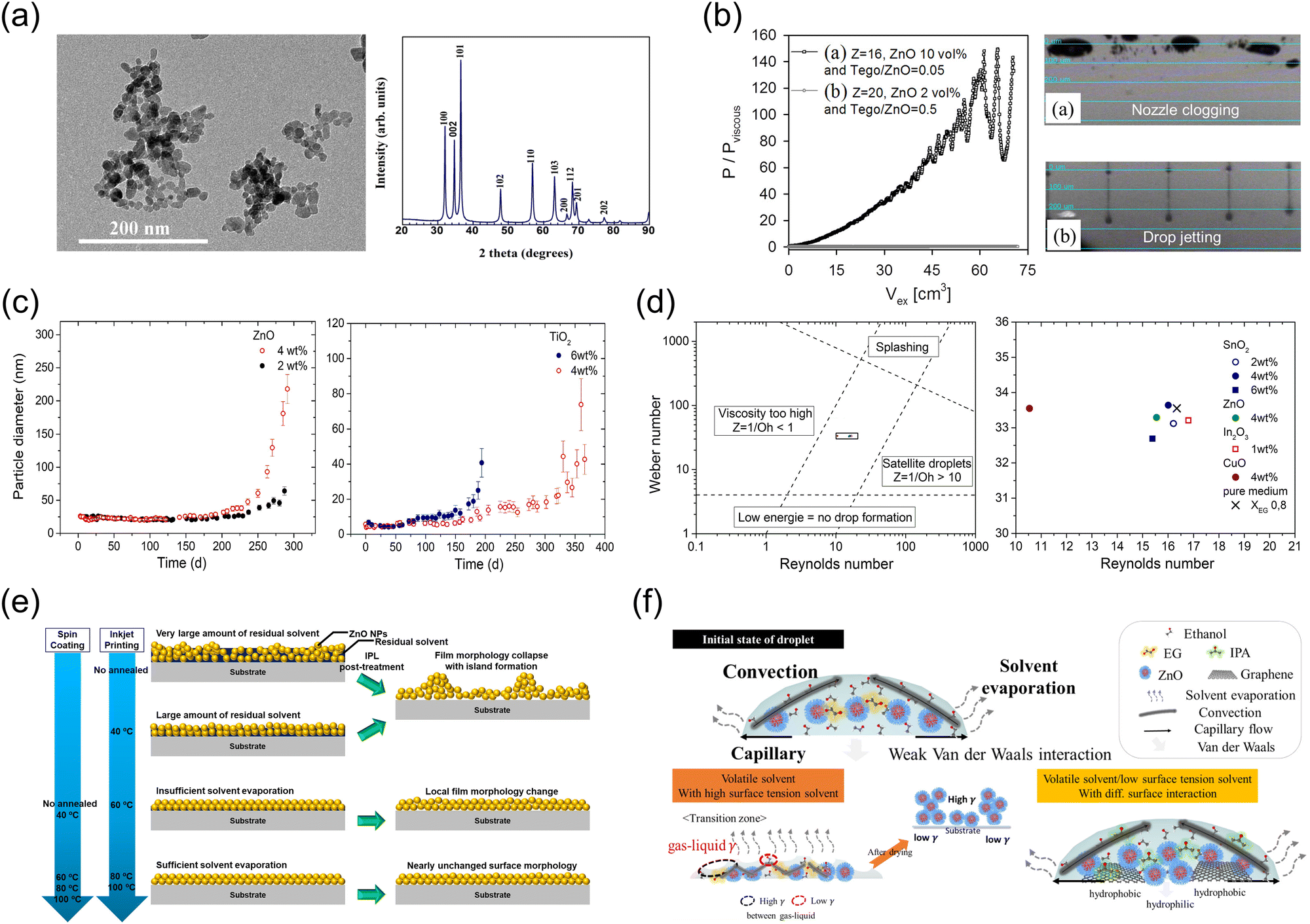 | ||
| Fig. 4 (a) Transmission electron microscopy (TEM) image and X-ray diffraction (XRD) patterns of ZnO NP aggregates. Reproduced with permission from ref. 46 Copyright 2018 IOP Publishing. (b) Nozzle clogging due to flow-induced aggregation of ZnO NPs. Reproduced with permission from ref. 47 Copyright 2012 American Chemical Society. (c) and (d) Particle diameter of ZnO and TiO2 as a function of storage time, and Reynolds number/Weber number region for jettable ink in the case of SnO2, ZnO, In2O3, and CuO NPs. Reproduced with permission from ref. 48 Copyright 2018 Elsevier. (e) Influence of intense pulsed light (IPL) on the surface morphology of inkjet-printed ZnO NPs. Reproduced with permission from ref. 28 Copyright 2021 American Chemical Society. (f) Visualization of the drying dynamics of a droplet containing ZnO NPs, highlighting the capillary flows, evaporation patterns, and nanoparticle aggregation. Reproduced with permission from ref. 120 Copyright 2020 American Chemical Society. | ||
In particular, to pattern MO NPs on large display panels, methods beyond lab-scale spin-coating and unsuitable thermal evaporation are required. Photolithography offers high precision and can be used to create complex multilayer patterns, ensuring consistency in large-scale production.14 However, this process is costly due to the need for specialized equipment. In contrast, transfer printing offers more flexibility, lower cost, and generates less waste, making it more environmentally friendly.121 However, it lacks the high resolution of traditional photolithography, may face alignment issues that affect display quality and the durability of the transferred layers. Thus, inkjet printing distinguishes itself from photolithography and transfer printing due to its advantages.122 It directly deposits material where needed, avoiding the etching or lifting steps required in other methods, thus minimizing waste and simplifying the process for faster and more economical production. Additionally, it does not use high temperatures or harsh chemicals common in other lithographic processes, making it suitable for a wider range of substrates, including heat-sensitive materials essential for flexible and lightweight applications.120 These benefits make inkjet printing a highly adaptable and cost-effective technology. However, several major bottlenecks pose significant challenges.
(1) Sensitivity to particle size: MO NPs exhibit size-dependent optoelectronic properties due to quantum confinement effects.56 As particle size decreases, the bandgap widens, carrier separation improves, and recombination losses are reduced. However, the increased surface-to-volume ratio of smaller NPs introduces a higher density of surface states,123 which can trap charge carriers and impede conductivity. Managing these effects requires precise control over NP size during synthesis, which can be challenging for large-scale production. Surface passivation or doping techniques are often employed to mitigate adverse surface effects50 but complicate the manufacturing process further.
(2) Challenges in inkjet printing: NPs are prone to agglomeration due to their high surface energy, which often leads to the clogging of inkjet printing nozzles and inconsistent deposition on substrates.47,50 This agglomeration complicates achieving uniform and stable NP dispersion, essential for the integration of NP-based ETLs. Furthermore, controlling ink viscosity and drying dynamics is challenging due to the small size and high surface area of the NPs,120 critical for achieving the uniform layer thickness required for optimal electronic device performance.
(3) Ink stability and reproducibility: maintaining long-term stability and reproducibility of NP inks is crucial for reliable large-scale production. However, issues such as sedimentation, particle growth during storage, and changes in ink chemistry over time can alter ink properties.48 These changes lead to variations in the quality and reproducibility of the printed films.
MO NPs commonly aggregate due to their high surface energy, driven by their small size and large surface area (Fig. 4a).46 This instability causes them to clump together, thereby decreasing their surface area relative to volume. Additionally, the strong van der Waals forces, due to their proximity within the medium, along with inadequate electrostatic repulsion, further promote aggregation, resulting in the formation of larger particle clusters. In inkjet printing, the parameter Z = Oh−1 is crucial for determining the jettability of a fluid, which refers to how well a fluid can form stable jets.47,48 This parameter is the inverse of the Ohnesorge number (Oh), a dimensionless number describing the fluid dynamics of small liquid volumes, particularly balancing viscous, inertial, and surface tension forces. The formula is  , where η is the viscosity of the fluid, ρ is the density, σ is the surface tension, and L is a characteristic length (typically the nozzle diameter). A higher Z value indicates that fluid inertia and surface tension are dominant over viscous forces, favorable for jetting as it promotes the breakup of the fluid into droplets rather than streaming or forming irregular shapes. However, for a fluid to be considered jettable, the Z value must lie between 1 and 10; outside of this range, fluids may be too viscous or too fluid, leading to poor print quality.
Willenbacher et al. investigated the challenges of nozzle clogging due to flow-induced aggregation of ZnO NPs (Fig. 4b).47 While Newtonian fluids were successfully jetted within a Z range of 2.5 to 26, ZnO NP suspensions experienced non-jetting and clogging within the same range due to aggregation at the nozzle exit. The study found that nozzle clogging correlates with pressure increases during extrusion through the ring-slit, with micrometer-sized aggregates acting as nuclei for further aggregation of nanoscale particles in the contraction zone. Aggregates between 1 and 6 μm were particularly problematic, causing clogging even though they are smaller than the nozzle diameter. To avoid clogging, the researchers suggested introducing a stabilizer and increasing the driving voltage to reduce ink exposure to elongational flow fields, which helps break up existing aggregates or prevent their formation. This study highlighted the need to consider additional colloidal stability parameters beyond the classical inverse Ohnesorge number (Oh) to optimize NP ink formulations for inkjet printing.
Furthermore, various MOs were characterized in terms of agglomeration. Gebauer et al. prepared NP inks of TiO2, In2O3, CuO, and SnO2, focusing on their stability and suitability for printing (Fig. 4c).48 ZnO NPs displayed limited stability in pure ethylene glycol (EG), with concentrations up to 4 wt% remaining stable for approximately 200 days. However, ZnO NPs started to aggregate rapidly after 300 days. Stability diminished as the quantity of dispersed NPs increases from 2 to 4 wt% due to a higher collision rate and increased likelihood of inter-dot collisions. Similar results were observed for TiO2 NPs, where the particles remained stable for up to 300 days, after which they exhibited drastically increased aggregation behavior, and stability diminished as the particle density increased from 4 to 6 wt%. In contrast, CuO, In2O3, and SnO2 NPs dissolved in EG showed no significant agglomeration over approximately 800 days. Furthermore, in the region where Z is less than 1, the fluid viscosity is excessively high, preventing droplet formation (Fig. 4d). Conversely, in the region where Z exceeds 10, satellite droplets begin to form. The upper dashed line marks the onset of splashing when the fluid impacts the substrate surface, defined by the condition We0.5Re0.25 > 50. In the area below the lower dashed line, the Weber number (We) is less than 4, and the kinetic energy is too low to allow droplet formation. Thus, precise and systematic printability assessments are necessary using a map plotting the Weber number (We) against the Reynolds number (Re), with a zone indicating optimal droplet formation.
In addition to the MO material composition, doping MOs significantly affects the agglomeration characteristics of ZnO NPs. A study involving both DFT calculations and experiments has revealed that doping ZnO with Li+, Cu2+, and Al3+ influences agglomeration behavior.49 The aggregate size of the doped ZnO NPs followed a specific trend: Li-doped ZnO had smaller aggregates compared to Cu-doped ZnO, undoped ZnO, and AZO, which had the largest aggregates. This trend aligns with the quantity of –OH groups adsorbed on the surface of the NPs, indicating that dopants with lower electronegativity, such as Li+ and Cu2+, can reduce the adsorption of –OH groups, thereby limiting agglomeration. These findings suggest that the dopant electronegativity affects the strength of the interfacial dopant–oxygen bonds and the adsorption energies of the –OH groups, ultimately influencing the agglomeration behavior of the doped ZnO NPs. In particular, the Al dopant significantly impacts the agglomeration of ZnO NPs. As the mass concentration of AZO NPs increased from 1.8% to 10%, the viscosity of the solution also rose from 6.9 cPs to 8.7 cPs.50 When direct inkjet printing of AZO was attempted at a low concentration of 1.8%, printhead nozzle clogging was relatively controlled despite multiple dispersions of AZO NPs. However, at a higher concentration of 10%, challenges arose, including difficulty in controlling droplet ejection due to the formation of satellite droplets and changes in the drop direction from the initial printing attempts. Additionally, rapid clogging of the cartridges was observed at this higher concentration, complicating the printing process and hindering continuation into the second day of printing with 10% AZO NPs. In addition to inkjet printing, spin-coating MO NPs also requires careful consideration of the solvent system, particularly regarding optimal viscosity and volatility. Ethanol was identified as the optimal solvent, providing balanced properties that minimized void formation due to its volatility and reduced agglomeration issues due to its appropriate viscosity.124
Achieving a neat morphology in ZnO NP films after inkjet printing also requires careful consideration. Cho et al. demonstrated that a higher annealing temperature is necessary for inkjet-printed ZnO NP films to fully evaporate the residual solvent and achieve a desirable surface morphology compared to films produced by spin-coating (Fig. 4e).28 Specifically, the optimal annealing temperature for spin-coated films was found to be 60 °C, while for inkjet-printed films it was 80 °C. The presence of residual solvent was found to quickly deteriorate the surface morphology, adversely affecting device performance. Furthermore, they investigated the effects of intense pulsed light (IPL) post-treatment on the film characteristics and subsequent QLED performance. Although IPL post-treatment following low-temperature annealing effectively evaporated the residual solvent, it caused rapid drying, leading to a more pronounced collapse of the film surface morphology and reduced device efficiency. These findings highlight the importance of selecting an appropriate annealing temperature to ensure complete solvent evaporation and maintain the stability of the underlying QD EML.
While the influence of the solvent system is crucial for spin-coating, its impact is equally significant when drying droplets formed by inkjet printing. The drying of a droplet containing ZnO NPs is influenced by a complex interplay of physical phenomena, such as convection, capillary flow, solvent evaporation, and van der Waals interactions (Fig. 4f), all of which are heavily affected by the choice of solvent.120 The selection of solvents, particularly cosolvents, is critical because they affect the surface tension, which directly influences the spreading behavior and evaporation rates of the droplet. When a droplet is deposited on a substrate, evaporation begins at the liquid–air interface, and the evaporation pattern is influenced by the solvent's surface tension. A lower surface tension allows the droplets to spread more broadly and evenly, mitigating the coffee-ring effect where NPs tend to accumulate at the perimeter. Adjusting the surface tension using cosolvents can promote more uniform spreading and evaporation, which are crucial for forming a flat, evenly distributed NP film. The dynamics within the droplet, such as convection driven by temperature gradients and capillary flow that pulls the liquid from the center to the edges as the droplet shrinks, are also determined by the solvent properties. The choice of cosolvent can modify these dynamics and affect the distribution of particles within the droplet. Additionally, the van der Waals forces between the NPs, which promote aggregation as the solvent evaporates, are influenced by the dielectric properties of the solvent. Certain cosolvents can alter these interactions, potentially controlling the aggregation levels, and thus affecting the smoothness and uniformity of the final film.120 In conclusion, the effective production of a flat and uniform film of ZnO NPs by inkjet printing requires meticulous selection and balancing of the solvent system to optimize surface tension, evaporation rate, fluid dynamics, and particle interactions.
3.3. Surface defects and positive aging
Understanding the degradation behavior in light-emitting diodes is essential for ensuring performance consistency and prolonging their operational lifetime. Typically, degradation follows a predictable pattern, often represented by an exponential or double exponential function, as expressed in the equation L/L0 = ae−kintt + be−kdegt.125 This mathematical representation facilitates dynamic adjustments in driving voltage and current, thereby maintaining uniform luminance and color accuracy over time.126 However, QLEDs that use MO NPs as an ETL may display an atypical aging characteristic termed ‘positive aging,’ where luminance unexpectedly improves rather than deteriorates initially (Fig. 5). This anomaly complicates the maintenance of consistent display quality, as the compensatory mechanisms within the panel's driving algorithms struggle to adapt to unconventional degradation patterns, potentially causing uneven luminance, color shifts, and visual inconsistencies.126 Thus, accurately predicting the degradation behavior of QLEDs is essential for enhancing product reliability. Despite the significance of these challenges, recent studies have tended to overlook or underestimate the implications of positive aging, focusing instead on instances where increased luminance has ostensibly extended the device lifetime. The phenomenon of positive aging in QLEDs continues to provoke debate and is the subject of active investigation. The subsequent sections will delve into pivotal benchmark studies concerning the positive aging observed in QLEDs, emphasizing both the ongoing debates and the research efforts aimed at comprehending and optimizing this phenomenon to improve performance and reliability.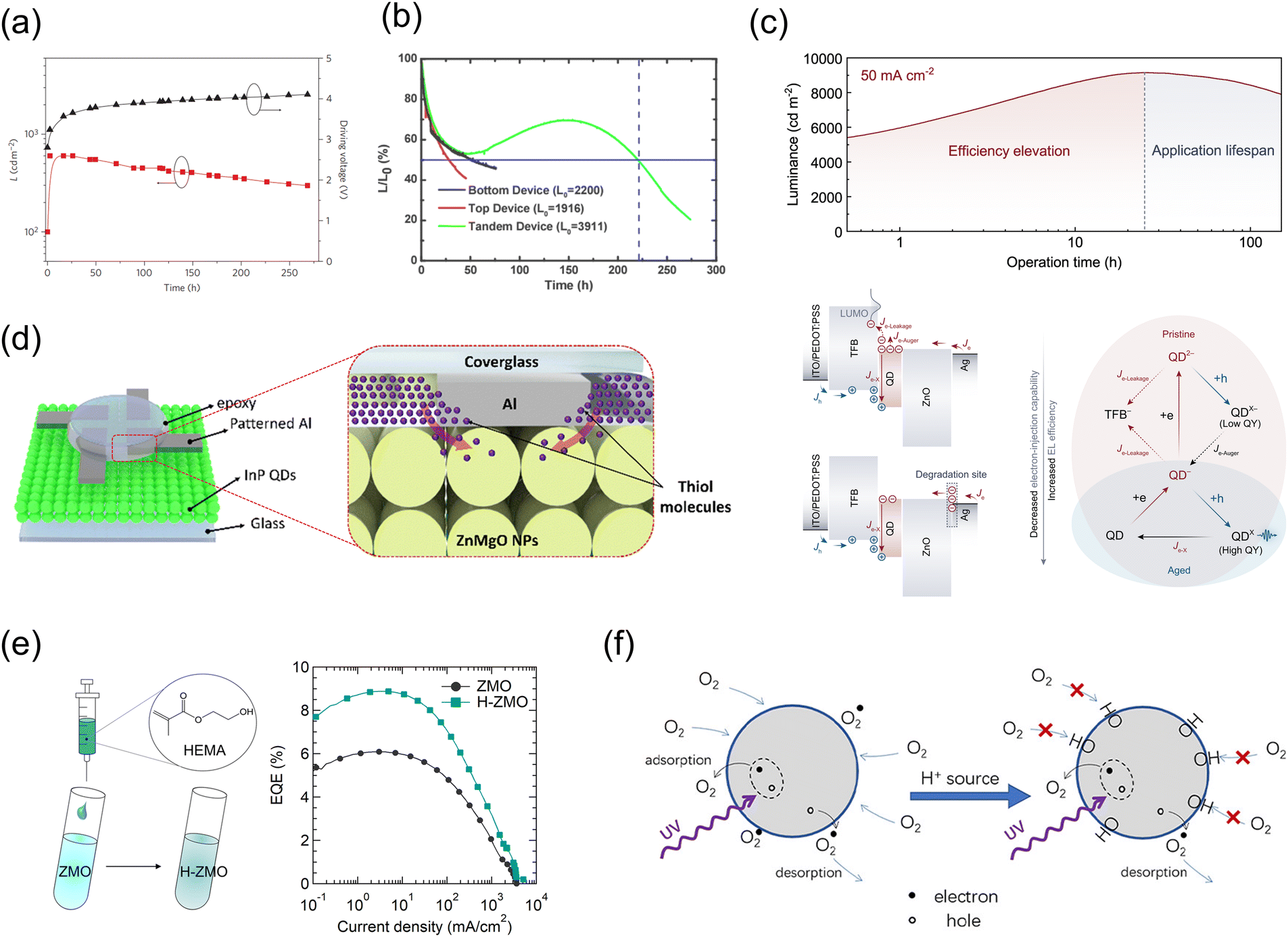 | ||
| Fig. 5 (a) Increasing luminance at a constant current density upon operation time. Reproduced with permission from ref. 53 Copyright 2011 Springer Nature. (b) Arbitrary aging heavior of tandem QLEDs upon operation time. Reproduced with permission from ref. 105 Copyright 2017 American Chemical Society. (c) Exploration of the EL process in QDs before and after efficiency improvement, highlighting the degradation in electron injection capability. Reproduced with permission from ref. 34 Copyright 2023 Springer Nature. (d) Diffusion of thiol molecules within an epoxy resin referred as a primary reason for positive aging. Reproduced with permission from ref. 127 Copyright 2023 Royal Society of Chemistry. (e) 2-Hydroxyethyl methacrylate (HEMA) additive for premixing ZnMgO NPs for positive aging effect. Reproduced with permission from ref. 98 Copyright 2024 Royal Society of Chemistry. (f) O2 adsorption on the ZnO NP surface elucidated as the positive aging mechanism, where the gradual formation of hydroxylated ZnO (HO–ZnO) stabilize the surface. Reproduced with permission from ref. 128 Copyright 2020 American Chemical Society. | ||
Xue and Holloway first documented the operational lifetime of QLEDs and observed that the luminance of these devices increased beyond initial levels after the first 2 h of operation (Fig. 5a).53 Along with the study, the phenomenon of positive aging in QLEDs has been frequently observed in numerous studies, and it is notable that instances of this behavior are often detected and mentioned even in research not primarily focused on positive aging (Fig. 5b).70,105 In 2013, Kazlas et al. conducted a detailed analysis of the increased luminance in QLEDs over time.68 The authors suggested that the primary cause of this luminance increase is the restoration of charge neutrality. Initially, strong electron coupling between the QDs and ZnO facilitates charge transfer from the QDs to ZnO, resulting in positively charged QDs. Upon operation, electrons reinject from ZnO back to the QDs, restoring electron/hole balance through a process termed ‘charge reneutralization,’ thereby enhancing emission efficiency and reliability. This mechanism involves the transfer of holes from positively charged QDs to midgap states in adjacent ZnO, rapidly neutralizing the QDs and allowing the recombination of previously transferred electrons with newly transferred holes in ZnO.
The term ‘positive aging’ was first introduced by Holloway et al. in 2017 to describe the phenomenon in which QLEDs exhibit an increase in luminance over time.45 In their study, the QLEDs were coated with a UV-curable acidic resin and subjected to either shelf-aging in a glove box or thermal annealing. Although specific details regarding the acidic resin are not provided in this paper, patents by the same group indicated the use of specific commercial products (Loctite 349, Loctite 352, and Loctite 366).129 The resin was applied dropwise onto the fully fabricated QLEDs with a cover glass placed on top to evenly spread the resin by weight. This treatment led to increases in the initial EQE values for RGB QLEDs; red QLEDs saw an increase from 8.5 to 12.7%, green from 8.5 to 19.2%, and blue from 6 to 9.6%, with corresponding decreases in leakage currents. The positive aging of QLEDs occurs when a weak acid in the resin reacts with the ZnO surface, producing water that combines with ambient CO2 to form carbonic acid. This acid then reacts with ZnO to form zinc carbonate. Owing to the lack of CO2 control in the glove box and UV-curing in ambient air, CO2 infiltrates the device, aiding the formation of zinc carbonate. This compound is believed to decrease the defect density in the ZnO NPs and modify the ZnO interfaces with QDs or Al, thereby enhancing the radiative recombination rate.
Following the initial identification of positive aging in QLEDs, researchers proposed a mechanism for this phenomenon observed in conventional QLEDs utilizing Al as the top electrode.130 This study suggested that the Al electrode gradually reacts with oxygen from the ZnMgO layer, leading to the formation of AlOX and the accumulation of VO at the Al/ZnMgO interface. This reaction promotes electron injection due to the formation of an alloyed AlZnMgO interface and the enhanced conductivity of ZnMgO. Furthermore, the interfacial AlOX acts as a barrier to electron trapping, effectively suppressing exciton quenching by the metal electrode. Overall, the study revealing the formation of an alloyed interface at the QD/ETL aligns with various studies suggesting that the QD/ETL interface significantly influences the aging behavior of QLEDs. Additionally, the research group examined the differing charge balance behaviors of CdSe- and InP-based QLEDs in terms of positive aging.131 Generally, CdSe-based QLEDs show excess electron injection, whereas InP-based QLEDs exhibit excess hole injection, necessitating adjustments to decrease hole injection and increase electron injection.
In alignment with these findings, another study reported that reduced interface exciton quenching at the QD/ZnMgO interface is a secondary effect, with the primary driver being enhanced electron injection at this interface.132 This improvement is primarily attributed to the diffusion of Al into the ZnMgO ETL, boosting electron mobility within ZnMgO and at its interface with Al. Post-encapsulation, initial EQE measurements showed an increase from 1.72 to 2.77%, with a further notable increase to 12.58% over 51.5 hours. These changes suggest that while exciton quenching passivation is initially dominant, improvements in Al-induced electron injection become predominant over time. Contributing factors include the facilitation of Al diffusion by acrylic acid in the resin and water molecules acting as electron donors, enhancing the conductivity of ZnMgO. Particularly, in blue-emitting QLEDs, positive aging effects are primarily observed in the NP forms of ZnO due to increased electron injection at the QD/ZnMgO interface. The insertion of polyethylenimine (PEI) at the ZnMgO/Al interface demonstrated consistent aging effects, but its placement at the QD/ZnMgO interface eliminated the aging effect, highlighting that enhanced electron injection at the QD/ZnMgO interface is critical to aging.
However, some reports contradict previous findings by stating that the operation-induced efficiency variation is due to a degradation in electron injection capability at the MO ETL/cathode interface (Fig. 5c),34 challenging earlier studies that suggested an increase in electron injection during positive aging. Analysis of the surface potential using operando cross-sectional scanning Kelvin probe microscopy of both pristine and aged QLEDs revealed a significant increase in the surface potential near the Ag interface in the positively aged device, indicating the emergence of a strong electric field at the ZnO/Ag interface. The underlying reason for the efficiency increase related to the ZnO/Ag interface is as follows: In pristine QLEDs, the high electron mobility in the ZnO layer and efficient electrical contact at the ZnO/Ag interface resulted in a higher space-charge concentration of electrons compared to holes in the QD layer. High electron concentration in the QD layer led to competition between electron and hole injection at the HTL/QD interface. This resulted in the conversion of some of the injected electron currents into nonradiative recombination currents through Auger recombination, along with electron leakage from the QD layer. Consequently, the exciton-generation efficiency of the pristine device was relatively low. As the electron injection capability decreases due to aging and increased resistance at the ZnO/Ag interface, the space-charge distribution across the QLED evolves, leading to the accumulation of more electrons at the electron injection interface and fewer electrons in the QD layer. This reduction in electron concentration in the QD layer decreases the rate of nonradiative recombination and leakage currents, thereby improving the conversion ratio of injected electrons to excitons.
In addition to the electron injection properties, the influence of chemical components within the resin has also been extensively studied. Jin et al. examined the effects of UV-curable acrylic resin components (acrylic acid, N,N-dimethylacrylamide, and isobornyl acrylate) on QLED devices under a nitrogen atmosphere through vapor treatment.133 Among these components, acrylic acid was found to induce positive aging effects comparable to those of the full UV-curable acrylic resin, suggesting that the acidic components in UV-curable acrylic resins trigger positive aging. Further investigation involved treating the QLEDs with vaporized isobutyric acid to explore the broader impact of organic acids. This study identified two primary mechanisms for positive aging: organic acid-facilitated silver interdiffusion into the MO ETLs, significantly enhancing electron conductivity, and the modification of ZnMgO NP surfaces by reacting with surface –OH groups to increase the density of surface carboxylate groups. This acid treatment also effectively suppressed exciton quenching at the QD/oxide interface, enhancing both the photoluminescence quantum yield (PLQY) and average PL lifetime of the QD films. These modifications at the QD/oxide interface by the mild organic acid treatment did not alter the optical properties of the pristine QD films but increased the EQEs in the aged QLED devices.
A recent study suggested that the diffusion of thiol molecules within an epoxy resin is another primary reason for positive aging (Fig. 5d).127 Assessing the PL and EL properties of the encapsulated QLED (ITO/PEDOT:PSS/poly(9,9-dioctylfluorene-alt-N-(4-sec-butylphenyl)-diphenylamine) (TFB)/QD/ZnMgO/Al with epoxy and cover glass) at daily intervals showed a recovery in the PL and a concurrent increase in the EL performance as aging progressed. The device initially exhibited an improved CE owing to lower charge injection at the Von. PL and EL enhancements were visually confirmed through sequential imaging, showing a widening green emission area and blue emission beneath the QD layer due to PL from the TFB. The thiol groups in the epoxy resin diffused from the edge to the center of the active region, reducing exciton quenching by ZnMgO and Al, and thereby recovering the PL loss. The fundamental mechanism is attributed to thiol-containing crosslinking agents, which alleviate exciton quenching and reduce nonradiative recombination channels. This diffusion restores the PL intensity by reducing the number of defect states in ZnMgO, which typically trap excitons. Additionally, the diffusion of epoxy components under the patterned Al cathode contributed to a gradual increase in luminance.
Moreover, a subsequent study examined the individual components of Loctite 366, including 2-hydroxyethyl methacrylate (HEMA), isobornyl methacrylate, hydroxyalkyl methacrylate, and acrylic acid, added directly to ZnMgO (Fig. 5e).98 Echoing the findings of Jin et al.,133 this research noted enhancements in efficiency and lifetime with acrylic acid, while isobornyl methacrylate and hydroxyalkyl methacrylate exhibited no significant changes. Notably, HEMA, which constitutes approximately 30–35% by weight of Loctite 366,134 significantly boosted QLED device performance. Key observations included a 0.4 eV upshift in the energy level of HEMA-doped ZnO, which facilitated better electron injection. Specifically, an increase in OV and –OH groups was noted, indicating higher electron concentration and surface –OH groups, factors believed to contribute to performance enhancement in QLEDs.
An alternative mechanism focusing on the effects of positive aging of ZnO in shelf-aged states, rather than those involving resins, was also proposed (Fig. 5f).128 This study examined changes in an ITO/ZnO NP/Al EOD before and after positive aging and found no significant differences in electron mobility or concentration within the ZnO NPs. This result contradicts earlier studies that reported variations in electron mobility. However, electro–absorption analysis revealed that aging notably increased the built-in potential (Vbi) of the photodiode, enhancing electron transport. Further experiments involving O2 adsorption elucidated the aging mechanism, demonstrating that the gradual formation of hydroxylated ZnO (HO–ZnO) decreased the number of active adsorption sites and stabilized the surfaces of the NPs.
A post-annealing process has been suggested as a method to optimize QLED device performance, producing effects similar to those observed with positive aging.135,136 Detailed analyses indicated that these improvements primarily stem from improved carrier injection for both electrons and holes, with a particularly effective enhancement in electron injection. Another study described an initial increase in the brightness and efficiency of QLEDs as a warm-up effect.137 This phenomenon significantly enhances the overall device performance after several I–V sweeps or during short-term operation. Interestingly, this phenomenon is reversible: the positive aging effects diminish when the device is turned off or subjected to a moderate post-annealing process. Steady-state and transient equivalent circuit analyses indicated that the current through the QDs increased due to a reduced carrier injection barrier, suggesting that reversible positive aging can be attributed to the filling of shell traps with excessive electrons during device operation.
While previous articles focused on the positive aging of ZnO or ZnMgO NP-based ETLs, recent research has increasingly focused on using SnO2 NPs as the ETL in QLEDs as an alternative solution to address positive aging issues.114 A critical distinction is that while ZnMgO can exhibit visible PL emission due to recombination between electrons in the CBM and trapped electrons in midgap states, SnO2 does not facilitate recombination at midgap states, thereby eliminating visible PL emission. Additionally, while ZnO demonstrated an increase in flat-band voltage from 1.07 V to 1.49 V after 14 days of shelf aging, TMAH-treated SnO2 maintained a consistent value of 1.71 V, indicating no change in the electron injection barrier.113 Furthermore, mobility measurements before and after shelf aging demonstrated that ZnO-based EODs exhibited an increase from 6.31 × 10⁻⁴ to 4.41 × 10⁻³ cm2 V−1 s−1, reflecting the variable electrical characteristics of ZnO due to positive aging. In contrast, TMAH-treated SnO2 EODs exhibited consistent mobility at 1.57 × 10⁻³ cm2 V−1 s−1, indicating that TMAH-SnO2 NPs are relatively immune to the effects of positive aging. Alongside TMAH treatment, Mn doping has been reported as an effective method to modify the surface of SnO2 NPs.115 Unlike ZnO, where surface VO can react with encapsulation resin or various adsorbates causing positive aging, Mn-doped SnO2 effectively controls these surface vacancies. Consequently, devices utilizing Mn-doped SnO2 exhibit superior shelf stability and are free from the effects of positive aging.
Comprehensively, the pronounced positive aging effects observed in ZnO or ZnMgO NPs have spurred research into alternative substitutes for MO NPs. While positive aging effects are most frequently associated with ZnO, they are also evident in ZnMgO130,135 and even in SnO2-based QLEDs,61 which were previously noted as being resistant to such effects. This suggests that MO NP-based QLEDs inherently face the challenge of positive aging to varying degrees, due to complex mechanisms and environmental factors. These findings underscore the necessity for ongoing exploration of material properties and device designs that can mitigate the impact of positive aging across different MO NPs within QLED technology.
4. Metal oxide and organic-combined electron transport layer
Combining MO NPs with organic molecules in mixed or bilayer configurations leverages the strengths of both components (Fig. 6). Bilayer configurations take advantage of the distinct properties of each layer; MOs enhance robustness and electron mobility,19 while organic molecules introduce flexibility and tunability to optimize optical properties.138 In mixed configurations, the close interaction between MOs and organic compounds optimizes charge transfer, facilitating efficient carrier separation and reducing recombination rates.139 These strategic integrations open new avenues for the development of materials with enhanced and tunable properties, paving the way for advancements in QLED technology.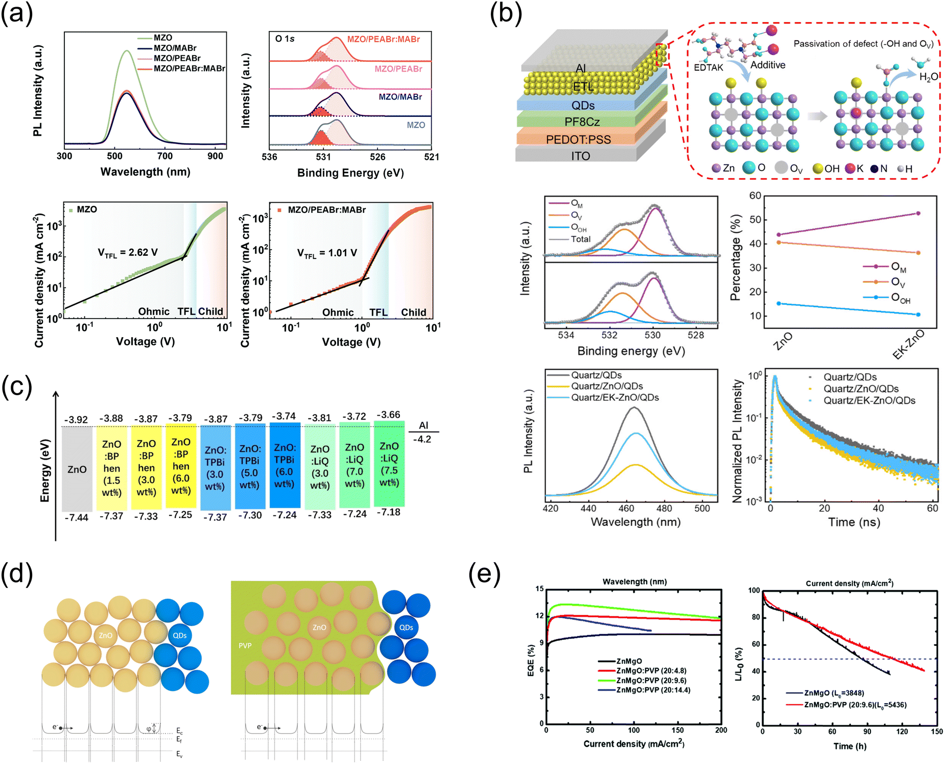 | ||
| Fig. 6 (a) PEABr:MABr dipole modulation layer at the ZnMgO/Al interface. Reproduced with permission from ref. 140 Copyright 2022 Royal Society of Chemistry. (b) Ethylenediaminetetraacetic acid dipotassium salt (EDTAK) as a bifunctional additive for ZnO NPs to passivate surface defects. Reproduced with permission from ref. 27 Copyright 2023 Royal Society of Chemistry. (c) Doping ZnO with lithium quinolate (Liq) and 2,2′,2′′-(1,3,5-benzinetriyl)-tris(1-phenyl-1H-benzimidazole) (TPBi) to control electron injection and reduce interfacial exciton quenching. Reproduced with permission from ref. 139 Copyright 2019 Elsevier. (d) New transport model for ZnO modified with PVP, proposing that PVP polymer chains increase the spacing between NPs, thereby reducing mobility. Reproduced with permission from ref. 141 Copyright 2018 Elsevier. (e) Improved EQE and operational lifetime of ZnMgO:PVP-induced QLEDs due to improved charge balance and reduction of leakage current. Reproduced with permission from ref. 142 Copyright 2019 Royal Society of Chemistry. | ||
4.1. Bilayer configurations
Conjugated polyelectrolytes are crucial in the development and enhancement of QLEDs, especially as ETMs. These specialized polymers are characterized by their conjugated backbone structures, featuring alternating single and double bonds that enable the delocalization of π-electrons. This structure facilitates efficient electron transport across the polymer chain, which enhances the electrical properties of QLEDs.A notable example is poly [(9,9-bis(3′-(N,N-dimethylamino)propyl)-2,7-fluorene)-alt-2,7-(9,9-dioctylfluorene)] (PFN), which aids in electron injection from the cathode directly into the QDs,30,121,143 thereby improving the lifetime of QLEDs. Lim et al. highlighted the use of PFN in InP QLEDs, demonstrating enhanced device performance through efficient exciton recombination within structurally engineered QDs with composition-gradient shells.30 The integration of PFN within QLEDs, either as part of the ETL or as a functional additive, is essential for enhancing interlayer interactions, enabling effective charge management, and aligning energy levels across the device.
Dielectric polymers, such as PMMA, are also employed as interlayers between the ETL and the QD EML.19,70 PMMA is chosen for its excellent film-forming capabilities, optical clarity, and effectiveness in minimizing interfacial exciton quenching. The primary role of PMMA and similar dielectric polymers is to form a physical and electronic barrier that prevents excitons from migrating from the QD EML to the ETL, where they could otherwise recombine nonradiatively.
tert-Butyldimethylsilyl chloride-modified poly(p-phenylene benzobisoxazole) (TBS-PBO) has also become a prominent interlayer material in QLEDs due to its excellent thermal and chemical stability, which enhances device durability and performance.144,145 TBS-PBO's primary function is to minimize exciton quenching at the interface, ensuring efficient utilization of excitons within the EML. Unlike typical insulating layers that impede current flow when their thickness exceeds the optimal value,19 TBS-PBO effectively reduces exciton quenching and controls electron injection without significantly hindering electron conductivity.144 This balance prevents the undesirable reduction in current often observed with other insulating layers. Additionally, TBS-PBO's robust characteristics make it exceptionally suitable for maintaining the structural and electronic integrity of QLEDs under operational stress,145 thereby ensuring high efficiency and long device lifetimes.
Recent studies have also explored the use of materials from perovskite solar cells as interlayers in QLEDs to stabilize interfaces between the QDs and the ETL.140,146 Aromatic amine functionalized organic molecules, such as phenylethylammonium bromide (PEABr) and phenylethylammonium iodide (PEAI), are used to fabricate two-dimensional (2D) perovskite layers that enhance stability against environmental degradation and modify electronic properties, such as bandgap tuning, crucial for light absorption and emission.147 Methylammonium bromide (MABr) aids in forming three-dimensional (3D) perovskites, enhancing light absorption and energy conversion efficiency.148 In QLEDs, these perovskite materials act as interlayers to reduce exciton quenching, ensure efficient electron injection, and improve luminance and device efficiency. For instance, Wang et al. demonstrated that incorporating a PEABr:MABr interlayer at the ZnMgO/Al interface significantly reduced contact resistance and upshifted the CBM of ZnMgO, thereby inhibiting excessive electron injection (Fig. 6a).140 This effect was attributed to the formation of an interfacial dipole at the ZnMgO/Al interface due to PEABr:MABr. Additionally, this interlayer filled and passivated surface defects in ZnMgO with Br− ions addressing VO in the matrix, effectively reducing defect concentrations from 7.0 × 10¹⁷ to 6.4 × 1016 cm−3. Furthermore, PEABr146 and CF3–PEAI149 have also been increasingly recognized for their effectiveness in passivating the surface of ZnMgO.
4.2. Mixed configurations
Incorporating additives directly into MO NPs prior to layer formation ensures uniform modification of the NP properties,139,150 essential for consistent charge transport and minimizing defects that can impair device functionality. The homogeneous mixing of additives with NPs enhances interface quality and effectively passivates surfaces to reduce trap states and other defects. This strategy not only simplifies the manufacturing process by eliminating separate layer deposition steps—thereby saving time and reducing complexity—but also improves material utilization and device efficiency. Direct interactions between additives and NPs fine-tune their electronic properties, stability, and solubility, leading to enhanced device performance and reliability.Traditionally, ethanolamine has been used as an additive in ZnO NPs, serving as a stabilizer that reduces defects and electron density while shallowing the CBM to improve charge injection balance.150 However, recent advancements have seen a variety of materials employed as additives, broadening the scope for optimizing ZnO NPs for enhanced performance across various applications. For instance, Cai et al. utilized ethylenediaminetetraacetic acid dipotassium salt (EDTAK) as a bifunctional additive for ZnO NPs to passivate surface defects and induce chemical doping (Fig. 6b).27 Typically, low-temperature-processed ZnO NPs exhibit an open hexagonal lattice, with Zn occupying half of the tetrahedral sites, leading to defects such as Zni and OV, as well as –OH groups formed during synthesis. To address this, materials such as PMMA, PFN, PEI, or metal doping (Mg, Li, Al, Sn, Ga) are employed to stabilize ultrathin layers, although these can present challenges such as ineffective electron blocking, tunneling effects in thin layers, or increased resistance in thicker layers. However, this study, effectively utilized EDTAK as a ZnO additive, passivating –OH and OV defects and making the CBM shallower to restrict excessive electron injection. The acidic carboxyl groups of EDTAK react with basic –OH groups on ZnO surfaces, reducing oxygen-bearing groups and enhancing ZnO stability through chelation, which forms stable complexes with surface Zn2+ ions, preventing agglomeration and enhancing colloidal stability. Notably, EDTAK also alters the work function, as evidenced by measurements showing a shift from 3.8 eV for ZnO to 3.53 eV for EDTAK-treated ZnO and a change in the CBM from −3.97 to −3.69 eV, thereby increasing the electron injection barrier. This adjustment impedes electron injection at the EK-ZnO/Al interface, aiding charge balance and reducing space-electron accumulation at the QD/ETL interface, which in turn minimizes interface degradation in QLEDs.
Further research by Liu et al. has demonstrated that doping ZnO with small molecules such as lithium quinolate (Liq) and 2,2′,2′′-(1,3,5-benzinetriyl)-tris(1-phenyl-1H-benzimidazole) (TPBi) can significantly enhance device performance, achieved by controlling electron injection and reducing interfacial exciton quenching (Fig. 6c).139 In brief, Liq is widely utilized to lower the cathode work function and enhance electron injection efficiency,151 while TPBi is used as an ETM due to its high triplet energy, which helps confine electrons and excitons within the EML.152 Along with the previous findings, Liu et al. showed that QLEDs using ZnO doped with 7.0 wt% Liq as the ETL displayed peak CE and EQE that were much higher than those in devices with undoped ZnO, attributable to effective electron blocking and reduced exciton quenching at interfaces.139 Both Liq and TPBi improved electron mobility by enhancing electron injection from ZnO to the QDs, with TPBi also serving to block holes, thereby maintaining the charge balance essential for stable operation.
Polyvinylpyrrolidone (PVP) is also commonly used to improve the uniformity and performance of ZnO NP films.141,142,153,154 The excellent film-forming properties, solubility enhancement, and NP stabilization capabilities of PVP are key to its usage. It acts as a surfactant, reducing surface tension and enhancing the spread and wetting of the solution on the substrate, leading to ETL films with fewer defects and a more uniform distribution of ZnO NPs.153 This uniformity is critical for efficient charge transport and minimizing electron recombination, thus enhancing device performance. Additionally, PVP influences the electronic properties of ZnO NPs by affecting their crystallinity and interacting with surface defects,154 potentially passivating traps that cause recombination. In particular, Sun et al. introduced a new transport model for ZnO modified with PVP, proposing that PVP polymer chains increase the spacing between NPs, thereby reducing mobility (Fig. 6d).141 Typically, when oxygen is adsorbed onto ZnO NP surfaces, it creates an interfacial potential barrier that facilitates charge movement via tunneling between the NPs. PVP extends the inter-NP distance, which further diminishes tunneling and reduces mobility. In the context of QLEDs, this increased spacing helps balance electron and hole injections, effectively acting as an insulating material. This arrangement reduces overall leakage current and decreases carrier back transfer from the QDs to ZnO at their interface. PVP not only enhances the compactness and surface morphology of ZnO or ZnMgO films but also mitigates the formation of voids typically caused by the agglomeration and clustering of NPs.142 Additionally, PVP increases the robustness of the ETL, making it more resistant to damage from sputtering processes used to deposit transparent electrodes, thereby facilitating the production of transparent QLEDs (Fig. 6e).
Comprehensively, although the concurrent use of MOs and organic semiconductors offers solutions to several issues associated with MOs, the inherent differences between these materials can complicate their integrated application, leading to increased material and production costs. In response to these challenges, there is growing interest in exploring the exclusive use of organic ETLs, which had previously been overlooked due to their lower efficiency and shorter lifetime.
5. Organic electron transport layer
One of the primary reasons for the reduced efficiency and shorter lifetime of QLEDs employing organic ETLs (Fig. 2) compared to MOs, is their insufficient electron injection efficiency.139 In QLEDs utilizing QDs for light emission, achieving a high electron mobility in the ETL is crucial. This high mobility ensures rapid and efficient electron delivery, optimizing light emission and maintaining a balanced electron/hole equilibrium in tandem with the inherently high electron mobility of QDs. However, as depicted in Fig. 3, organic ETLs exhibit significantly lower electron mobilities than MO NPs, primarily due to fundamental differences in molecular structures and charge transport mechanisms. Organic materials are composed of carbon-based molecules interconnected by Sigma (σ) and pi (π) bonds, with π-electrons delocalized across conjugated systems facilitating charge transport. However, these electrons are constrained within specific molecular pathways,155 restricting their mobility relative to MOs like ZnO. ZnO's crystalline structure enables a continuous conduction band in thin films and NPs, facilitating unrestricted electron movement. Conversely, morphological irregularities common in organic films hinder electron mobility.156 In organic materials, electron transport involves hopping between molecules, a slower process vulnerable to scattering and trapping.155Furthermore, organic materials are more susceptible to environmental factors such as oxidation and moisture,157 exacerbating electron mobility limitations. Thus, the intrinsic material properties of organic compounds largely account for their inferior electron mobility compared to MOs, contributing notably to the interfacial inefficiencies observed in early QLEDs incorporating organic ETLs.
5.1. Electron mobility and interfacial emission
Initially, QLEDs primarily employed organic materials as the ETLs until the effectiveness of MO NPs was recognized. The pioneering QLED study, reported by Colvin et al. in 1994, utilized PPV as a hole injection layer with CdSe QDs, employing either ITO or Mg electrodes without an additional ETL (Fig. 7a).158 Subsequent research efforts concentrated on enhancing stable electron injection, leading to the widespread adoption of Alq3 as an ETL. Introduced in the late 1980s by Tang, Slyke et al. at Eastman Kodak,159 Alq3 represented a significant breakthrough in OLED technology, serving both as an ETM and a green-emitting EML. Alq3's role in facilitating electron injection and transport from the cathode, coupled with its dual function in EL generation, laid a foundational framework for early OLED displays.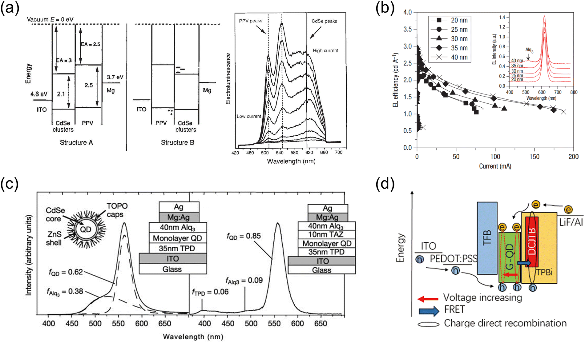 | ||
| Fig. 7 (a) Pioneering QLED structure utilizing PPV as a hole injection layer with CdSe QDs, employing either ITO or Mg electrodes without an additional ETL. Reproduced with permission from ref. 158 Copyright 1994 Nature Springer. (b) Interfacial emission peak due to Alq3 layer, intensifying the emission peak as the thickness increases. Reproduced with permission from ref. 160 Copyright 2007 Nature Springer. (c) Introduction of 3-(biphenyl-4-yl)-5-(4-tert-butylphenyl)-4-phenyl-4H-1,2,4-triazole (TAZ) as a HBL to address the interfacial peaks of Alq3. Reproduced with permission from ref. 161 Copyright 2002 Nature Springer. (d) Fluorescent emitter indicating both Förster resonant energy transfer (FRET) and direct charge injection in TPBi-induced QLEDs. Reproduced with permission from ref. 162 Copyright 2017 American Chemical Society. | ||
Similarly, its potential application in QLEDs involves optimizing the interface between QDs and the cathode to enhance charge injection and recombination processes. However, in QLEDs utilizing Alq3 as the ETL, increasing the thickness of Alq3 poses specific challenges. A thicker Alq3 layer intensifies the emission peak in the overall EL spectrum (Fig. 7b).160 This phenomenon arises from less efficient electron injection through Alq3 compared to hole injection from the HTL to the QD layer. Consequently, more holes bypass the QD layer and enter the ETL, where they are prone to nonradiative recombination rather than contributing to light emission at the EML. Thus, precise management of Alq3 thickness is crucial for maintaining optimal QLED performance, ensuring balanced charge injection and minimizing internal quenching, thereby safeguarding device efficiency and luminance.
However, the occurrence of the Alq3 peak in QLEDs varies depending on the device structure and is notably influenced by the type of QD and the specific dynamics of charge carriers corresponding to each color. In accordance to a former study, a white-emitting QLED employing a mixed monolayer of RGB QDs exhibited distinct behaviors according to the color emitted.163 For blue-emitting QLEDs, the HTL, N,N′-Bis(3-methylphenyl)-N,N′-diphenylbenzidine (TPD), encountered challenges in efficient hole injection. This resulted in electron leakage from the ETL to the HTL/QD interface, leading to emission peaks associated with exciplex formation or originating from the HTL itself rather than from Alq3. This occurred because the predominant recombination took place at the HTL/QD interface. Conversely, green-emitting QLEDs demonstrated effective hole injection from the TPD HTL, minimizing electron leakage and allowing holes to penetrate into the ETL. This facilitated enhanced emission from the Alq3 layer, showcasing a more balanced process of charge carrier injection and recombination with a prominent Alq3 peak. These complexities highlight the challenges in designing QLEDs with mixed QD layers, where the unique properties of each QD color and the corresponding characteristics of the transport layers critically influence overall device performance and emission characteristics.
To address the interfacial peaks of Alq3, Coe et al. effectively employed a hole-blocking layer (HBL), 3-(biphenyl-4-yl)-5-(4-tert-butylphenyl)-4-phenyl-4H-1,2,4-triazole (TAZ) (Fig. 7c).161 By incorporating TAZ as an interlayer between Alq3 and QDs, they achieved significant reduction in the proportion of the Alq3 peak from 38 to 9%, enhancing device performance. However, ongoing research has seen the rise of 2,2′,2′′-(1,3,5-benzinetriyl)-tris(1-phenyl-1H-benzimidazole) (TPBi) as a replacement for Alq3 and TAZ, demonstrating improved efficiency as an ETL.
TPBi is an organic semiconductor featuring a benzene core and three benzimidazole groups. TPBi has played a pivotal role not only in early-stage QLEDs but also in recent high-efficiency devices characterized by intricate interfacial emission pathways. Chen et al. demonstrated that doping the fluorescent emitter 4-(dicyanomethylene)-2-t-butyl-6-(1,1,7,7-tetramethyljulolidyl-9-enyl)-4H-pyran (DCJTB) into the charge transport layer (CTL) enabled monitoring of exciton RZ through Förster resonant energy transfer (FRET) between QDs and DCJTB (Fig. 7d).162 The study highlighted that the location of the RZ within QLEDs is profoundly influenced by the choice of ETL. For instance, in devices employing a ZnMgO ETL, the RZ initially resides near the QD/HTL interface. With increasing driving voltage, this zone shifts closer to the QD/ETL interface, albeit with limited overall movement. In contrast, devices utilizing TPBi as the ETL exhibit a different behavior: the RZ initiates near the QD/ETL interface and extends toward the HTL as voltage rises. This observation indicated a broader range of recombination compared to those with a ZnMgO ETL, suggesting that both FRET and direct charge recombination mechanisms significantly influence the emission characteristics of QLEDs induced by organic ETLs.
Furthermore, Hübner et al. provided new insights into the emission mechanisms of organic ETLs in inkjet-printed InP QLEDs.164 Their research underscored how device layouts and QD materials influence the physical origins of parasitic emission pathways. Notably, the presence of Liq dopant adjacent to QDs without a spacer increased parasitic emissions, while introducing a spacer between the QD and Liq layers tended to enhance exciplex-driven parasitic emissions at the interface. Moreover, embedding QDs in a matrix that conducts holes improved hole conductivity and localization within the EML, thereby reducing parasitic emissions primarily emanating from the matrix molecules rather than the QDs themselves. Thus, the optimal strategy to minimize parasitic emissions involves placing the Liq dopant near the QD layer and utilizing a hole-conducting matrix within the QD layer. This approach effectively restricts residual parasitic emissions to exciplex formation between the matrix material and Liq, resulting in nonradiative recombination. It underscores the critical role of spatial separation of dopants within the ETL to precisely control emission pathways.
5.2. Intrinsic instability
The inherent instability of organic ETMs primarily stems from their molecular compositions and structures. Organic semiconductors, composed of carbon-based molecules and polymers, typically feature intricate conjugated systems involving π-bonds and aromatic rings. These structural elements facilitate electron transport via delocalized π-electrons but render the materials susceptible to oxidative degradation when exposed to oxygen and other environmental factors.157 This degradation alters the electronic properties, thereby compromising device efficiency and longevity.Additionally, organic materials generally exhibit weaker bond strengths compared to their inorganic counterparts. Held together by van der Waals forces, hydrogen bonds, and π–π interactions, these bonds are less robust than the ionic and covalent bonds found in inorganic materials. Consequently, organic ETMs have lower thermal stability; under operational heat or environmental stress, these bonds can degrade, leading to physical deterioration such as crystallization165 or delamination166 of organic layers. Moisture susceptibility further contributes to the instability of organic ETMs. These materials are typically more hygroscopic, absorbing water that can cause hydrolysis or induce morphological changes, impacting electron mobility and introducing ionic impurities that degrade material performance.167 In contrast, inorganic ETMs such as MO NPs—like ZnO or ZnMgO—are preferred due to their chemical inertness and stability under operational conditions.168 Their strong ionic or covalent bonds and crystalline structure provide high operational stability and durability. In summary, while ongoing advancements in molecular engineering and encapsulation techniques continue to enhance the efficiency of organic ETMs, their inorganic counterparts inherently offer superior durability and stability. This makes inorganic ETMs preferable for high-performance applications where reliability and long-term operational stability are critical.
In fully fabricated optoelectronic device utilizing organic ETLs, degradation manifests through intricate processes influenced by their inherent roles in charge transport and light emission.157 One significant mechanism is crystallization, particularly pronounced during dark storage in small molecule devices, which alters electrical characteristics and exciton formation by lowering the ionization potential.169 A lower glass transition temperature (Tg) heightens the risk of crystallization, thereby shortening device lifetime. Moreover, the flow of charge carriers also contributes to degradation by generating non-luminous byproducts and gradually diminishing device brightness.170 Photobleaching poses another challenge as exposure to light triggers photochemical reactions that degrade adjacent organic ETMs’ electrical properties.171 Oxidation of organic layers further impairs devices as molecular oxygen and water react, creating exciton quenching sites.32 These processes reduce conjugation length, introduce charged defects, and increase trap density, thereby impeding charge flow. Thus, in the case of organic ETL-based QLEDs, thermal heating, moisture, and oxygen also sensitively contribute to degradation.57
Therefore, ensuring stability in both the QDs and ETMs is crucial for optimizing device performance and longevity. Efforts to develop stable organic ETLs resistant to diverse degradation factors are essential for extending the lifetimes of organic ETL-based QLEDs.
5.3. Advancements in organic electron transport layers
In the early stages of QLED development, organic ETLs such as Alq3, TAZ, and TPBi were widely employed.160,161,172 However, these materials have largely been supplanted by MO NPs over time, due to their superior charge transport efficiency. However, MO NPs also exhibit limitations such as abstruse surface chemistry, issues with NP agglomeration (Section 3.2), and reliability challenges under positive aging (Section 3.3). Consequently, there has recently been a resurgence of interest in using organic ETLs in QLEDs (Fig. 8). This renewed focus is driven by research demonstrating that organic ETLs can achieve efficiency and stability comparable to those of MO NPs. In the following sections, the discussion delves into specific organic ETL materials used in high-efficiency, long-lifetime QLED configurations. Their distinctive properties and contributions to advancing QLED technology without relying on MO NPs are highlighted.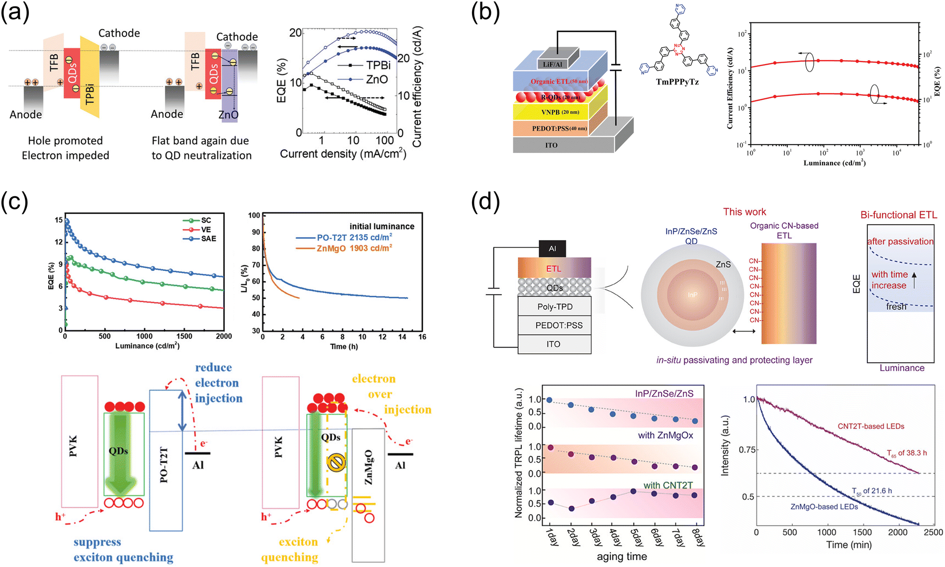 | ||
| Fig. 8 (a) Limitations of organic ETLs including TPBi regarding charge neutralization capability within QD EML. Reproduced with permission from ref. 173 Copyright 2021 John Wiley and Sons. (b) TmPPPyTz as an organic ETL for efficient (EQE 13.4%) QLEDs attributed to its minimal PL quenching and advantageous electron transfer characteristics. Reproduced with permission from ref. 22 Copyright 2020 John Wiley and Sons. (c) PO-T2T as an ETL for a record-high EQE of 15% and a T50 lifetime of 1430 h at an initial luminance of 100 cd m−2 in green-emitting InP QLEDs. Reproduced with permission from ref. 23 Copyright 2022 Copyright 2020 John Wiley and Sons. (d) CNT2T as an ETL for a record-high EQE of 15% in red-emitting InP QLEDs. Reproduced with permission from ref. 24 Copyright 2023 American Chemical Society. | ||
Polyethylenimine ethoxylated (PEIE) also plays a pivotal role as an interfacial layer in QLEDs, owing to its unique molecular structure that facilitates the formation of energy dipoles.176,177 PEIE can be processed into a thin film less than 10 nm thick under ambient conditions. It dissolves well in environmentally friendly solvents like water or alcohol and effectively shifts the work function of an ITO electrode from −4.7 eV to −3.08 eV.176 This property makes PEIE a promising candidate for an independent ETL. PEIE's backbone consists of ethylenimine units linked in a branched polymeric structure, with ethoxylation enhancing flexibility and polarity. The ethoxylated groups interact with surface atoms of adjacent layers such as the ETL or cathode, facilitating the formation of permanent or induced dipoles. These interactions create dipoles that modify the local electric field at the interface, thereby reducing the work function of the interface layer.
Castelli et al. demonstrated substantial advancements in QLED technology by developing fully solution-based devices using CdSe/CdS dot-in-rod (DiR) heterostructures and organic ETLs comprising polar/polyelectrolytic conjugated polymers, achieving EQEs of up to 6.1%.178 Specifically, three polyfluorene derivatives, denoted as p-P.1 to p-P.3, were synthesized as ETMs. These polymers shared the same π-conjugated backbone but differed in their polar/electrolytic functionalities. Octyl side chains were introduced to prevent intermolecular aggregation and crystallization during film formation. Films of these functionalized polymers displayed excellent film-forming properties when spin-coated from a methanol solution that did not dissolve DiRs, which were stabilized by specific hexylphosphonic and octadecylphosphonic acid ligands.
Moreover, recent research has emphasized the use of thin dielectric polymers as interlayers to mitigate excessive electron injection. While previous studies often utilized PMMA as the dielectric layer,19,70 TBS-PBO has emerged as an effective alternative for controlling electron injection.145 TBS-PBO has demonstrated the ability to block excess electrons while maintaining high QD emission efficiency. Unlike conventional insulating blocking layers, TBS-PBO offers improved conductivity, which sustains high current densities in devices. This balance between conductivity and electron-blocking capability has significantly enhanced QLED performance. For instance, pioneering research successfully utilized TBS-PBO to achieve a blue-emitting QLED with an EQE exceeding 17% with a notable luminance of 4635 cd m−2.145
Besides, TPBi offers shallower LUMO compared to the CBM of MO ETLs (Fig. 3). This characteristic enhances TPBi's effectiveness in injecting electrons into QDs with shallow CBMs, such as Cd-free QDs.182 Cd-based QDs typically feature a CBM around −4 eV, whereas Cd-free QDs range from −3.5 to −3.0 eV.131 For instance, Motomura et al. demonstrated that using TPBi in ZnS–AgInS2 QD-based QLEDs resulted in significantly higher efficiencies compared to ZnO NPs.182 Additionally, recent research by Chen et al. highlighted TPBi as an effective ETL for blue-emitting orthorhombic BN-based QLEDs, where BN QDs feature a CBM of −1.76 eV.183
TPBi not only transports electrons effectively to the EML but also serves as an efficient HBL.65,184 Incorporating TPBi into the HTL of QLEDs can also manipulate charge distribution and dynamics, resulting in enhanced device efficiency. QLEDs incorporating TPBi within HTL have demonstrated over a 30% increase in CE, achieving up to 25.0 cd A−1.184
TPBi is also known for effectively forming exciplexes when adjacent to HTL materials.185 An exciplex is a complex where two molecules, typically a donor and an acceptor, interact via charge transfer upon electronic excitation, exhibiting distinct emission spectra compared to their individual components. In QLEDs, exciplex formation between TPBi and HTLs is facilitated by their compatible energy levels and complementary electronic properties. Yang et al. utilized TPBi's properties to develop a white QLED with a high color rendering index of 95.185 The device combines red emission from an exciplex formed at the interface between the HOMO of poly-TPD (−5.2 eV) and the LUMO of TPBi (−3.2 eV), centered at a wavelength of 620 nm. This is complemented by green emission from QDs centered at 550 nm and weak blue emission around 430 nm due to parasitic emission from poly-TPD.
As discussed, although many papers have been published utilizing the advantages of TPBi, research on its precise luminescence mechanism is still actively ongoing. A significant aspect of these studies is the spectral overlap observed between the PL and absorption spectra of TPBi and the QDs, indicating efficient exciton energy transfer from TPBi to the QDs without significant back transfer.172 This efficient energy transfer enables the elimination of additional HBLs and supports the use of thicker QD films, resulting in EL spectra predominantly dominated by QD emissions. Moreover, while previous studies have primarily focused on TPBi's electron mobility and its role as a barrier for electron injection from a charge transfer perspective, deeper investigations have highlighted TPBi's dual functionality as an effective ETL for exciton energy transfer. For instance, Chen et al. conducted a comprehensive study using magneto-electroluminescence (MEL) as an in situ tool to analyze energy transfer and charge injection in TPBi-based QLEDs.186 Their analysis revealed that energy transfer from TPBi and the HTL to the QDs, facilitated by FRET, plays a crucial role in exciton formation and luminescence. Their findings contrasted with those of QLEDs based on ZnO, where direct charge injection predominantly drives the luminescence mechanism. In TPBi-based QLEDs, the primary mechanism is the energy transfer from the HTL to the QDs. This was further supported by MEL observations, which demonstrated increased changes with the strength of the external magnetic field in TPBi-based QLEDs but remained unchanged in ZnO-based QLEDs.
As discussed, in TPBi-based QLEDs, previous studies have indicated that excitons are primarily generated in the HTL and subsequently transferred to the QDs via energy transfer or FRET, with minor contribution from TPBi to QD transfer. However, recent work has further highlighted the predominant role of energy transfer from TPBi to QDs.162 Their research compared luminescence mechanisms in devices employing different architectures: one utilizing ZnMgO as the ETL and another using TPBi, with DCJTB employed as a fluorescent sensor in the CTL for deeper analysis. Their findings underscored that the choice of ETL significantly influences the location of the RZ. In devices with ZnMgO ETL, the RZ is confined within the QD layer, primarily facilitating direct charge recombination for QD emissions. In contrast, older device structures with TPBi as the ETL showed the RZ extending into the CTL, indicating that QD emission results from both direct charge recombination and FRET originating from the TPBi.
However, a few articles have noted TPBi's limitations regarding charge neutralization within QD EML. For instance, Sun et al. investigated the charge accumulation restoration capability of TPBi-based QLEDs (Fig. 8a).173 Studies suggest that QDs may start with a net positive68 or negative173 charge before operation, but not in a neutral state. Sun et al. specified that in TPBi-based QLEDs, QDs were negatively charged, accelerating hole injection starting at 0.5 V, whereas electron injection began at 3.0 V due to electron repulsion and facilitated hole injection by the negative charge.173 In contrast, when TPBi was replaced with ZnO, both holes and electrons started injecting at 1.7 V, indicating that this difference stemmed from charge transfer and neutralization processes between the QDs and ETLs. Unlike TPBi, ZnO helped neutralize initial accumulated charges in the QDs by matching midgap states with trapped charge energy states in the QDs, enabling smooth electron transfer between QDs, ZnO, and Al electrodes.
However, despite achieving high performance in QLEDs using ZnO as the ETL, significant challenges remain in industrial applications due to concerns about reliability and scalability as discussed in Section 3.2 and Section 3.3. Thus, researchers are emphasizing the importance of achieving neutral QDs without accumulated charges and better control of charge dynamics at HTL/QD and QD/ETL interfaces for the successful implementation of organic ETLs.
Specifically, 3TPYMB has become increasingly prominent as a component in mixtures of QDs with organic ETMs.190 This combination effectively prevents exciton quenching at the interface and, importantly, blocks hole current leakage, highlighting the role of 3TPYMB in enhancing the performance and stability of QLEDs through improved charge carrier management. A recent study reported that mixing green-emitting AgInGaS/GaS QDs with 3TPYMB significantly enhanced the performance of standalone QD EMLs.191 Without the ETM, a portion of the injected charge in QD-based devices bypasses the thin EML and fails to convert into light. However, the addition of 3TPYMB helped balance the carrier distribution within the EML. Specifically, 3TPYMB, which possesses deep energy levels, acts as an effective HBL that primarily enhances electron transport, as its energy levels align closer to the CBM of the QDs. The 3TPYMB layer was strategically placed at the base of the EML, effectively separating it from the QDs positioned at the top, thus serving as the HBL. Additionally, EMLs further mixed with the organic molecule 2,4-bis(3-(pyridin-3-yl)phenyl)-6 (TmPPyTz) displayed a more homogeneous mixture with evenly distributed QDs. Notably, when 3TPYMB and TmPPyTz were mixed with QDs, TmPPyTz blended more uniformly, whereas 3TPYMB tended to segregate toward the bottom. This configuration utilizes the superior electron transport and miscibility of TmPPyTz with the QDs, alongside 3TPYMB's effective hole-blocking capabilities. Such a strategic layered structure led to a significant enhancement in device performance, achieving an EQE of 5.4%, which surpassed the EQEs when TmPPyTz (2.7%) or 3TPYMB (1.9%) were used separately.191
Moreover, recent research has demonstrated TmPyPB's potential as a standalone organic ETL without the addition of MO NPs like ZnO or ZnMgO. In CdSe QD-based QLEDs, TmPyPB achieved an impressive EQE of 11.9%,194 showing its effectiveness in managing electron transport and enhancing device efficiency independently of MO components. TmPyPB has also been successfully employed as an ETL in blue-emitting ZnSeTe QD-based QLEDs, achieving a notable EQE of 4.06%,195 significantly higher than blue-emitting QLEDs excluding MO NPs. The success of TmPyPB in these applications is attributed to its dual role as a HBL and ETL, effectively enhancing charge carrier management and reducing recombination losses in QLED devices.
TmPPPyTz has also demonstrated lower operating voltages and higher efficiencies in QLEDs when blended with QDs compared to other ETMs such as 3TPYMB and TmPyPB.190 When incorporated with QDs, all three ETMs effectively prevent exciton quenching, thereby enhancing the efficiency of QLEDs utilizing only QDs in the EML. However, whereas 3TPYMB and TmPyPB led to higher operating voltages (3.6 V), TmPPPyTz maintained a lower voltage requirement (2.4 V), similar to devices without any mixed ETM. This lower voltage demand is attributed to the triazine moiety in TmPPPyTz, known for its role in achieving low driving voltages in OLEDs.197 Moreover, TmPPPyTz possesses advantageous properties for QLEDs, particularly concerning energy levels. A study demonstrated a QLED incorporating TmPPPyTz as an ETL achieving a respectable EQE of 10%, attributed to TmPPPyTz's superior prevention of hole leakage currents compared to other ETMs. Additionally, TmPPPyTz's relatively deep LUMO compared to other organic ETMs makes it exceptionally suitable for Cd-based QLEDs.22 This characteristic enables outstanding performance by effectively managing charge transport and minimizing loss mechanisms within the device.
In alignment with this research, Yang et al. conducted a detailed analysis of TmPPPyTz's effectiveness as an organic ETL, emphasizing that the interface between TmPPPyTz and QDs experiences minimal PL quenching due to its advantageous electron transfer characteristics (Fig. 8b).22 This is partly because organic ETLs typically have shallower LUMO levels than MO NPs, necessitating deeper LUMO levels to effectively align with the deep CBM of CdSe QDs. The research team compared the LUMO and HOMO energy levels of nitrogen heterocycle-containing compounds TmPyPB, B3PYMPM, and TmPPPyTz, which differ in their central cores (benzene, pyrimidine, and triazine) but share pyridine units. TmPyPB, B3PYMPM, and TmPPPyTz have LUMO levels of −2.28, −2.79, and −3.07 eV, respectively, and HOMO levels of −6.49, −6.57, and −7.20 eV, respectively. Moreover, the deeper LUMO and HOMO of TmPPPyTz enhanced its efficiency as an ETL in CdSe-based QLEDs by improving the energy-level matching and hole-blocking capabilities with CdSe QDs. Comparing TmPPPyTz to ZnO NPs, ZnO's CB of −4.40 eV offers even deeper matching, leading to more advanced I–V curves in ZnO-based devices. Despite this, the TmPPPyTz-based QLEDs (EQE 10.6%) outperformed those using ZnO NPs (EQE 5.2%) because TmPPPyTz provides a better balance in charge injection, as proven by experiments showing matching in the EOD and hole-only devices (HODs) for TmPPPyTz. This study suggested that further advances in organic ETL-based QLEDs require the development of materials with deeper LUMOs, similar to those in MOs. Achieving deep LUMO levels necessary for improved electron affinity and stability in organic ETLs involves complex molecular engineering, including the integration of strong electron-withdrawing groups to lower the LUMO.
Above all, due to its influential roles as an ETL, it is one of the most potent candidates for organic ETL in QLEDs. In 2022, Chen et al. utilized PO-T2T as an ETL to develop the highest EQE of 15% and promising lifetime with a T50 of 1430 h at an initial luminance of 100 cd m−2 in green-emitting InP QLEDs using an organic ETL (Fig. 8c),23 emphasizing its ability to prevent electron over-injection and accumulation when paired with InP QDs. In brief, PO-T2T exhibits an electron mobility ranging from approximately 1.7 × 10⁻³ to 4.4 × 10⁻³ cm2 V−1 s−1, significantly higher than traditional organic ETLs (Fig. 3). PO-T2T's LUMO of −2.8 eV and HOMO of −6.8 eV not only make it suitable for use as an ETL in InP QLEDs, due to good alignment with their energy levels, but its shallow LUMO compared to the CBM of ZnMgO also prevents spontaneous electron transfer and PL quenching at the QD and ETL interfaces. In particular, they involved a solution-assisted evaporation (SAE) method for layering PO-T2T, taking advantage of its easy dissolution in ethanol for a combination of spin-coating and thermal evaporation. Comprehensively, PO-T2T achieves high-efficiency InP QLEDs by effectively mitigating excessive electron transfer and exciton quenching through its lower electron mobility and high electron injection barrier. However, when PO-T2T was applied to Cd-based QLEDs instead of InP QLEDs, no improvements were observed, likely due to energy level mismatches between the Cd-based QDs and PO-T2T.
Beyond its role in InP QLEDs, PO-T2T is also utilized across various configurations as an organic ETL. A recent study underscored its efficacy in a high-performance, white-emitting QLED employing In3+-doped ZnCuGaS/ZnS QDs, achieving an EQE of 2.4% and a color rendering index of 94.9.198 This application underscores PO-T2T's versatility in Cd- and MO-free configurations, highlighting its potential in developing environmentally friendly yet high-quality lighting solutions. This progress underscores PO-T2T's pivotal role in meeting stringent environmental standards201 while advancing QLED performance.
![[triple bond, length as m-dash]](https://www.rsc.org/images/entities/char_e002.gif) N) plays a crucial role in passivating the ZnS surface. While the high concentration of VO in ZnMgO inorganic ETL acts as an oxidation source for the adjacent interface,130 the organic ETL instead passivates and protects traps on the ZnS outer shell. The ZnS (110) surface contains four primary defects: VS, zinc vacancies (VZn), interstitial sulfur (Si), and Zni, all contributing to deep trap states within the ZnS bandgap.203 VS and VZn, with lower defect-formation energies, are dominant in ZnS. However, applying CNT2T to ZnS increases the formation energies of all four defects, with the most significant passivation observed for VS. Comparing the binding energy of surface-passivated QDs with CNT2T to those with original ligands (oleylamine and oleic acid) but still possessing Zn2+ defects, CNT2T exhibits higher binding energy under both ambient and operational conditions, indicating effective trap passivation. Each corner of the CNT2T molecule, enriched with electron-dense CN groups, interacts strongly with uncoordinated Zn2+ ions. The non-planar structure of CNT2T enables two CN groups to approach the ZnS surface simultaneously, achieving dual-site passivation with a single molecule. Time-resolved photoluminescence (TRPL) lifetime and steady-state PLQY measurements revealed that QDs alone exhibit a lifetime of 10.8 ns and a PLQY of 68%. In contrast, ZnMgO/QD composites show reduced lifetimes of 7.2 ns and a PLQY of 49%. However, CNT2T/QD composites display enhanced performance with a lifetime of 9.5 ns and a PLQY of 57%, which further improves to 11.2 ns and 74%, respectively, after aging for 5 days in an N2 glovebox. This underscores CNT2T's superior ability to suppress exciton quenching compared to ZnMgO, consistent with DFT analysis indicating effective passivation of Zn2+ traps. Moreover, after 8 days of aging, TRPL lifetimes in InP and InP/ZnMgO films decreased, while InP/CNT2T films continued to exhibit increased lifetimes up to 5 days of aging. This suggests that CNT2T may require time for quasi-solid-state ligand exchange to passivate InP effectively. Transmission electron microscopy (TEM) and energy-dispersive X-ray spectroscopy (EDS) analyses revealed migration of VS from InP to ZnMgO and VO from ZnMgO to InP in devices using ZnMgO. In contrast, CNT2T devices exhibited VS only in InP without VO signals, indicating well-passivated and protected InP QDs. Notably, the mobility of CNT2T, approximately 5.8 × 10⁻⁴ cm2 V−1 s−1, is comparable to that of ZnMgO NPs. The LUMO of CNT2T at −2.8 eV aligns well with the CBM of InP QDs at −3.3 eV. Importantly, this study suggested that even in QLEDs employing only an organic ETL without MO NPs, positive aging effects can occur due to gradual passivation of Zn2+ defects in the InP/ZnSe/ZnS QD shell. However, these effects are less severe than those observed in QLEDs using ZnO or ZnMgO NPs, making organic ETLs advantageous for mitigating positive aging effects despite their milder manifestation.
N) plays a crucial role in passivating the ZnS surface. While the high concentration of VO in ZnMgO inorganic ETL acts as an oxidation source for the adjacent interface,130 the organic ETL instead passivates and protects traps on the ZnS outer shell. The ZnS (110) surface contains four primary defects: VS, zinc vacancies (VZn), interstitial sulfur (Si), and Zni, all contributing to deep trap states within the ZnS bandgap.203 VS and VZn, with lower defect-formation energies, are dominant in ZnS. However, applying CNT2T to ZnS increases the formation energies of all four defects, with the most significant passivation observed for VS. Comparing the binding energy of surface-passivated QDs with CNT2T to those with original ligands (oleylamine and oleic acid) but still possessing Zn2+ defects, CNT2T exhibits higher binding energy under both ambient and operational conditions, indicating effective trap passivation. Each corner of the CNT2T molecule, enriched with electron-dense CN groups, interacts strongly with uncoordinated Zn2+ ions. The non-planar structure of CNT2T enables two CN groups to approach the ZnS surface simultaneously, achieving dual-site passivation with a single molecule. Time-resolved photoluminescence (TRPL) lifetime and steady-state PLQY measurements revealed that QDs alone exhibit a lifetime of 10.8 ns and a PLQY of 68%. In contrast, ZnMgO/QD composites show reduced lifetimes of 7.2 ns and a PLQY of 49%. However, CNT2T/QD composites display enhanced performance with a lifetime of 9.5 ns and a PLQY of 57%, which further improves to 11.2 ns and 74%, respectively, after aging for 5 days in an N2 glovebox. This underscores CNT2T's superior ability to suppress exciton quenching compared to ZnMgO, consistent with DFT analysis indicating effective passivation of Zn2+ traps. Moreover, after 8 days of aging, TRPL lifetimes in InP and InP/ZnMgO films decreased, while InP/CNT2T films continued to exhibit increased lifetimes up to 5 days of aging. This suggests that CNT2T may require time for quasi-solid-state ligand exchange to passivate InP effectively. Transmission electron microscopy (TEM) and energy-dispersive X-ray spectroscopy (EDS) analyses revealed migration of VS from InP to ZnMgO and VO from ZnMgO to InP in devices using ZnMgO. In contrast, CNT2T devices exhibited VS only in InP without VO signals, indicating well-passivated and protected InP QDs. Notably, the mobility of CNT2T, approximately 5.8 × 10⁻⁴ cm2 V−1 s−1, is comparable to that of ZnMgO NPs. The LUMO of CNT2T at −2.8 eV aligns well with the CBM of InP QDs at −3.3 eV. Importantly, this study suggested that even in QLEDs employing only an organic ETL without MO NPs, positive aging effects can occur due to gradual passivation of Zn2+ defects in the InP/ZnSe/ZnS QD shell. However, these effects are less severe than those observed in QLEDs using ZnO or ZnMgO NPs, making organic ETLs advantageous for mitigating positive aging effects despite their milder manifestation.
6. Future directions and closing remarks
In this review, current research trends on ETLs in QLEDs, focusing on MO NPs and organic semiconductors, are analyzed. While ZnO or ZnMgO NPs have predominantly been used in high-efficiency and long-lifetime QLED studies, it is clear that MO NPs also face challenges that need addressing for commercial viability. Recently, organic ETLs, which had initially emerged but faded in the early stages, have seen renewed interest in recent literature.In terms of efficiency and operational lifetime, QLEDs with MO NP ETLs currently outperform those with organic ETLs. However, considering factors such as scalability for mass production, balanced research and development efforts are essential for both MO NPs and organic ETLs. In the following paragraphs and Fig. 9, the differences between MO NP- and organic-based ETLs are summarized based on the review and outlined the challenges that need addressing for each technology's commercialization.
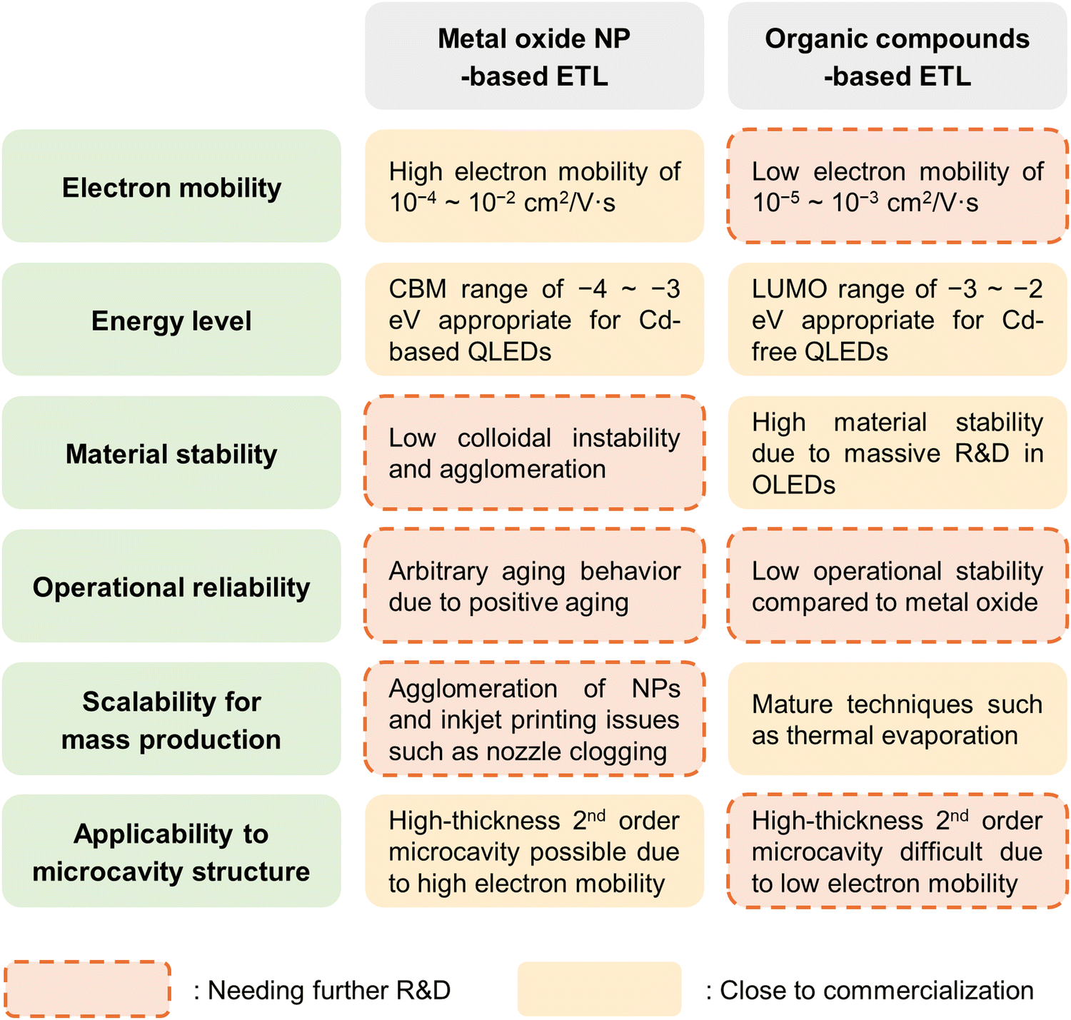 | ||
| Fig. 9 Future directions for QLEDs with MO NPs- and organic compounds-based ETLs in the aspect of electron mobility, energy level, materials stability, operational reliability, scalability for mass production, and applicability to microcavity structure. | ||
(1) Traditional organic ETLs typically exhibit lower electron mobility compared to MO NPs. The rapid electron and hole injection required for QD EMLs, which emit light through the recombination of singlet or triplet excitons, necessitates efficient electron injection followed by accelerated hole injection due to confinement-enhanced Coulomb interactions. Jin et al. elucidated a nanoscopic sequential electron/hole injection mechanism that initiates exciton formation and light emission through initial electron injection, followed by hole injection.34 This process utilizes the intermediate negatively charged state of QDs to enhance hole injection and prevent excessive electron injection.
(2) Energy level alignment is crucial; traditional organic ETLs typically have shallower LUMO levels, generally above −3.0 eV, compared to MOs with typical CBMs of approximately −4.0 eV. Cd-based QDs also feature CBMs around −4.0 eV, posing challenges for energy level alignment with organic ETLs. However, recent studies indicate that Cd-free QDs, such as InP QDs exhibit better compatibility with the energy levels of modern high-efficiency organic ETLs.
(3) Material stability is crucial in advancing efficient QLEDs. MO NPs often face challenges like agglomeration, particularly problematic for applications like inkjet printing in large-area displays. Despite limited studies on mitigating ZnO NP agglomeration, organic ETLs must meet stringent material stability criteria. Organic ETLs, extensively developed for OLEDs, generally exhibit superior shelf stability compared to MO NPs. However, to ensure compatibility with QDs and effective charge neutrality, ongoing enhancements in material stability are imperative. Recent studies on bifunctional organic ETLs, such as CNT2T, show promise in passivating Zn2+ defect states on QD surfaces, addressing charge issues and boosting device performance.
(4) Operational stability remains a concern: devices based on organic ETLs lag behind MO NP-based counterparts in both Cd-based and Cd-free QLEDs. This shortfall stems from the inherent instability of organic ETMs and their interactions at the QD interface. Nevertheless, significant strides have been made in improving operational lifetimes, as evidenced by green Cd-free QLEDs using organic ETLs, which now approach lifetimes comparable to those of MO NP-based devices.
(5) Scalability for mass production favors organic ETLs due to established deposition techniques inherited from OLED manufacturing. MO NP-based ETLs rely on solution processes such as inkjet printing, which have inherent challenges such as nozzle clogging attributed to NP agglomeration.
In conclusion, the review explored the material aspects of ETLs in QLED research and development, particularly contrasting MO NPs with organic alternatives. While current efforts primarily focus on enhancing efficiency and lifetime within established frameworks, addressing inherent challenges linked to MO NPs in mass production and exploring organic ETLs as viable alternatives are crucial. This review will offer a valuable roadmap for future research directions essential for the successful commercialization of QLEDs, underscoring its potential as the next-generation display technology after OLEDs.
Author contributions
J. Kim: conceptualization, validation, investigation, writing – original draft, writing – review & editing, funding acquisition.Data availability
This article is a review and synthesizes previously published literature. It does not contain any new experimental data. All sources and articles that have been reviewed and discussed are cited appropriately within the text. Supplementary materials referenced in the review are available from the corresponding author upon reasonable request.Conflicts of interest
There are no conflicts to declare.Acknowledgements
This work was supported by the National Research Foundation of Korea (NRF) grant (RS-2022-00166348) funded by the Korea government (MSIT). This work was also supported by the Gachon University research fund of 2024(GCU- 202400700001). The author would like to thank Editage (https://www.editage.co.kr) for English language editing.References
- C. Yuan, F. Tian and S. Chen, Nano Res., 2023, 16, 5517–5524 CrossRef CAS
.
- H. Li, S. Zhou and S. Chen, Laser Photonics Rev., 2023, 17, 2300371 CrossRef CAS
- Y. Wang, Y. Yang, D. Zhang, T. Zhang, S. Xie, Y. Zhang, Y.-B. Zhao, X. Mi and X. Liu, Adv. Mater., 2023, 35, 2306703 Search PubMed
- H. Shen, Q. Gao, Y. Zhang, Y. Lin, Q. Lin, Z. Li, L. Chen, Z. Zeng, X. Li, Y. Jia, S. Wang, Z. Du, L. S. Li and Z. Zhang, Nat. Photonics, 2019, 13, 192–197 Search PubMed
- Y. Liu, F. Li, Z. Xu, C. Zheng, T. Guo, X. Xie, L. Qian, D. Fu and X. Yan, ACS Appl. Mater. Interfaces, 2017, 9, 25506–25512 Search PubMed
- Y. Sun, Y. Jiang, X. W. Sun, S. Zhang and S. Chen, Chem. Rec., 2019, 19, 1729–1752 CrossRef CAS PubMed
- X. Yang, D. Zhao, K. S. Leck, S. T. Tan, Y. X. Tang, J. Zhao, H. V. Demir and X. W. Sun, Adv. Mater., 2012, 24, 4180–4185 CrossRef CAS PubMed
- K. Masaoka, Y. Nishida, M. Sugawara and E. Nakasu, IEEE Trans. Broadcast., 2010, 56, 452–457 Search PubMed
- S. J. Dain, B. Kwan and L. Wong, J. Opt. Soc. Am. A, 2016, 33, A300–A305 CrossRef PubMed
- C. Jo, J. Kim, J. Y. Kwak, S. M. Kwon, J. B. Park, J. Kim, G.-S. Park, M.-G. Kim, Y.-H. Kim and S. K. Park, Adv. Mater., 2022, 34, 2108979 CrossRef CAS PubMed
- H. Shen, Q. Lin, W. Cao, C. Yang, N. T. Shewmon, H. Wang, J. Niu, L. S. Li and J. Xue, Nanoscale, 2017, 9, 13583–13591 RSC
- Y. Joshi and J. M. Brown, presented in part at the 2019, 18th IEEE Intersociety Conference on Thermal and Thermomechanical Phenomena in Electronic Systems (ITherm), May 28–31, 2019.
- J. Kim, J. Roh, M. Park and C. Lee, Adv. Mater., 2024, 36, 2212220 CrossRef CAS PubMed
- J. Zhao, L. Chen, D. Li, Z. Shi, P. Liu, Z. Yao, H. Yang, T. Zou, B. Zhao, X. Zhang, H. Zhou, Y. Yang, W. Cao, X. Yan, S. Zhang and X. W. Sun, Nat. Commun., 2021, 12, 4603 CrossRef CAS PubMed
- S. Scalbi, V. Fantin and F. Antolini, J. Cleaner Prod., 2017, 142, 3702–3718 CrossRef CAS
- S.-Y. Yoon, Y.-J. Lee, H. Yang, D.-Y. Jo, H.-M. Kim, Y. Kim, S. M. Park, S. Park and H. Yang, ACS Energy Lett., 2022, 7, 2247–2255 CrossRef CAS
- Y. Lee, H.-M. Kim, J. Kim and J. Jang, J. Mater. Chem. C, 2019, 7, 10082–10091 RSC
- C. Jiang, Z. Zhong, B. Liu, Z. He, J. Zou, L. Wang, J. Wang, J. Peng and Y. Cao, ACS Appl. Mater. Interfaces, 2016, 8, 26162–26168 CrossRef CAS PubMed
- X. Dai, Z. Zhang, Y. Jin, Y. Niu, H. Cao, X. Liang, L. Chen, J. Wang and X. Peng, Nature, 2014, 515, 96–99 CrossRef CAS PubMed
- H. Zhang, X. Sun and S. Chen, Adv. Funct. Mater., 2017, 27, 1700610 CrossRef
- L. Yang, X. Li, Q. Yang, S. Wang, H. Tian, J. Ding and L. Wang, Chem. Eng. J., 2022, 436, 135221 CrossRef CAS
- L. Yang, X. Li, Q. Yang, S. Wang, H. Tian, J. Ding and L. Wang, Adv. Funct. Mater., 2021, 31, 2007686 CrossRef CAS
- P. Gao, Y. Zhang, P. Qi and S. Chen, Adv. Opt. Mater., 2022, 10, 2202066 CrossRef CAS
- Y.-K. Wang, H. Wan, J. Xu, Y. Zhong, E. D. Jung, S. M. Park, S. Teale, M. Imran, Y.-J. Yu, P. Xia, Y.-H. Won, K.-H. Kim, Z.-H. Lu, L.-S. Liao, S. Hoogland and E. H. Sargent, J. Am. Chem. Soc., 2023, 145, 6428–6433 CrossRef CAS PubMed
- A. P. Kulkarni, C. J. Tonzola, A. Babel and S. A. Jenekhe, Chem. Mater., 2004, 16, 4556–4573 CrossRef CAS
- K. Ding, H. Chen, L. Fan, B. Wang, Z. Huang, S. Zhuang, B. Hu and L. Wang, ACS Appl. Mater. Interfaces, 2017, 9, 20231–20238 CrossRef CAS PubMed
- F. Cai, Y. Tu, D. Tian, Y. Fang, B. Hou, M. Ishaq, X. Jiang, M. Li, S. Wang and Z. Du, Nanoscale, 2023, 15, 10677–10684 RSC
- Y. J. Han, K.-T. Kang and K. H. Cho, ACS Appl. Mater. Interfaces, 2021, 13, 50111–50120 Search PubMed
- S.-K. Kim, H. Yang and Y.-S. Kim, J. Appl. Phys., 2019, 126, 185702 CrossRef
- J. Lim, M. Park, W. K. Bae, D. Lee, S. Lee, C. Lee and K. Char, ACS Nano, 2013, 7, 9019–9026 CrossRef CAS PubMed
- Q. Wu, F. Cao, S. Wang, Y. Wang, Z. Sun, J. Feng, Y. Liu, L. Wang, Q. Cao, Y. Li, B. Wei, W.-Y. Wong and X. Yang, Adv. Sci., 2022, 9, 2200959 CrossRef CAS PubMed
- W. Zhang, B. Li, C. Chang, F. Chen, Q. Zhang, Q. Lin, L. Wang, J. Yan, F. Wang, Y. Chong, Z. Du, F. Fan and H. Shen, Nat. Commun., 2024, 15, 783 CrossRef CAS PubMed
- B. S. Ong, C. Li, Y. Li, Y. Wu and R. Loutfy, J. Am. Chem. Soc., 2007, 129, 2750–2751 CrossRef CAS PubMed
- Y. Deng, X. Lin, W. Fang, D. Di, L. Wang, R. H. Friend, X. Peng and Y. Jin, Nat. Commun., 2020, 11, 2309 CrossRef CAS PubMed
- S. Wang, Y. Guo, D. Feng, L. Chen, Y. Fang, H. Shen and Z. Du, J. Mater. Chem. C, 2017, 5, 4724–4730 RSC
- J. Pan, J. Chen, Q. Huang, Q. Khan, X. Liu, Z. Tao, Z. Zhang, W. Lei and A. Nathan, ACS Photonics, 2016, 3, 215–222 CrossRef CAS
- S. Cao, J. Zheng, J. Zhao, Z. Yang, C. Li, X. Guan, W. Yang, M. Shang and T. Wu, ACS Appl. Mater. Interfaces, 2017, 9, 15605–15614 Search PubMed
- L. Zhang, Y. Chen, S. Cao, D. Yuan, X. Tang, D. Wang, Y. Gao, J. Zhang, Y. Zhao, X. Yang, Z. Lu, Q. Fan and B. Sun, Adv. Sci., 2024, 11, 2402756 CrossRef CAS PubMed
- J. Lim, Y.-S. Park and V. I. Klimov, Nat. Mater., 2018, 17, 42–49 CrossRef CAS PubMed
- J. Roh, Y.-S. Park, J. Lim and V. I. Klimov, Nat. Commun., 2020, 11, 271 CrossRef CAS PubMed
- H. Jung, Y.-S. Park, N. Ahn, J. Lim, I. Fedin, C. Livache and V. I. Klimov, Nat. Commun., 2022, 13, 3734 Search PubMed
- N. Ahn, C. Livache, V. Pinchetti, H. Jung, H. Jin, D. Hahm, Y.-S. Park and V. I. Klimov, Nature, 2023, 617, 79–85 CrossRef CAS PubMed
- N. Ahn, Y.-S. Park, C. Livache, J. Du, K. Gungor, J. Kim and V. I. Klimov, Adv. Mater., 2023, 35, 2206613 CrossRef CAS PubMed
- Y. Gong, T. Andelman, G. F. Neumark, S. O’Brien and I. L. Kuskovsky, Nanoscale Res. Lett., 2007, 2, 297 CrossRef CAS
- K. P. Acharya, A. Titov, J. Hyvonen, C. Wang, J. Tokarz and P. H. Holloway, Nanoscale, 2017, 9, 14451–14457 RSC
- K. S. Suganthi, K. Harish, N. M. Nair and P. Swaminathan, Flexible Printed Electron., 2018, 3, 015001 CrossRef
- A. Lee, K. Sudau, K. H. Ahn, S. J. Lee and N. Willenbacher, Ind. Eng. Chem. Res., 2012, 51, 13195–13204 CrossRef CAS
- J. S. Gebauer, V. Mackert, S. Ognjanović and M. Winterer, J. Colloid Interface Sci., 2018, 526, 400–409 CrossRef CAS PubMed
- Z.-Y. Chen, W.-Z. Shao, W.-J. Li, X.-Y. Sun, L. Zhen and Y. Li, ACS Appl. Nano Mater., 2022, 5, 10809–10817 CrossRef CAS
- O. Shavdina, C. Grillot, A. Stolz, F. Giovannelli, V. Bertagna, J. Nicolle, C. Vautrin-Ul, C. Boulmer-Leborgne and N. Semmar, J. Coat. Technol. Res., 2021, 18, 591–600 CrossRef CAS
- K. Cheong, U. Jo, W. P. Hong and J. Y. Lee, Small Methods, 2024, 8, 2300862 CrossRef CAS PubMed
- G. Hong, X. Gan, C. Leonhardt, Z. Zhang, J. Seibert, J. M. Busch and S. Bräse, Adv. Mater., 2021, 33, 2005630 CrossRef CAS PubMed
- L. Qian, Y. Zheng, J. Xue and P. H. Holloway, Nat. Photonics, 2011, 5, 543–548 CrossRef CAS
- E. Y. Shaba, J. O. Jacob, J. O. Tijani and M. A. T. Suleiman, Appl. Water Sci., 2021, 11, 48 CrossRef CAS
- H.-Y. Lu, S.-Y. Chu and S.-S. Tan, J. Cryst. Growth, 2004, 269, 385–391 CrossRef CAS
- M. Jay Chithra, M. Sathya and K. Pushpanathan, Acta Metall. Sin., 2015, 28, 394–404 CrossRef CAS
- F. Wang, Z. Wang, X. Zhu, Y. Bai, Y. Yang, S. Hu, Y. Liu, B. You, J. Wang, Y. Li and Z. A. Tan, Small, 2021, 17, 2007363 CrossRef CAS PubMed
- Y. Sun, W. Wang, H. Zhang, Q. Su, J. Wei, P. Liu, S. Chen and S. Zhang, ACS Appl. Mater. Interfaces, 2018, 10, 18902–18909 CrossRef CAS PubMed
- A. K. Diallo, M. Gaceur, S. Fall, Y. Didane, S. Ben Dkhil, O. Margeat, J. Ackermann and C. Videlot-Ackermann, Mater. Sci. Eng. B, 2016, 214, 11–18 CrossRef CAS
- S. Wei, J. Miao, Q. Shi, S. Shao and L. Zhang, J. Mater. Sci.: Mater. Electron., 2021, 32, 9795–9803 CrossRef CAS
- J. Gao, M. Liu, X. Shi and D. Pan, New J. Chem., 2024, 48, 8631–8637 RSC
- J. W. Stouwdam and R. A. J. Janssen, J. Mater. Chem., 2008, 18, 1889–1894 RSC
- P. O. Anikeeva, C. F. Madigan, J. E. Halpert, M. G. Bawendi and V. Bulović, Phys. Rev. B: Condens. Matter Mater. Phys., 2008, 78, 085434 CrossRef
- Q. Sun, G. Subramanyam, L. Dai, M. Check, A. Campbell, R. Naik, J. Grote and Y. Wang, ACS Nano, 2009, 3, 737–743 Search PubMed
- W. K. Bae, J. Lim, M. Zorn, J. Kwak, Y.-S. Park, D. Lee, S. Lee, K. Char, R. Zentel and C. Lee, J. Mater. Chem. C, 2014, 2, 4974–4979 RSC
- J. Kwak, W. K. Bae, D. Lee, I. Park, J. Lim, M. Park, H. Cho, H. Woo, D. Y. Yoon, K. Char, S. Lee and C. Lee, Nano Lett., 2012, 12, 2362–2366 CrossRef CAS PubMed
- T. Zhou, T. Wang, J. Bai, S. Liu, H. Zhang, W. Xie and W. Ji, Adv. Mater., 2024, 36, 2313888 CrossRef CAS PubMed
- B. S. Mashford, M. Stevenson, Z. Popovic, C. Hamilton, Z. Zhou, C. Breen, J. Steckel, V. Bulovic, M. Bawendi, S. Coe-Sullivan and P. T. Kazlas, Nat. Photonics, 2013, 7, 407–412 CrossRef CAS
- S. Jia, M. Hu, M. Gu, J. Ma, D. Li, G. Xiang, P. Liu, K. Wang, P. Servati, W. K. Ge and X. W. Sun, Small, 2024, 20, 2307298 CrossRef CAS PubMed
- Q. Lin, L. Wang, Z. Li, H. Shen, L. Guo, Y. Kuang, H. Wang and L. S. Li, ACS Photonics, 2018, 5, 939–946 CrossRef CAS
- H. Zhang, N. Sui, X. Chi, Y. Wang, Q. Liu, H. Zhang and W. Ji, ACS Appl. Mater. Interfaces, 2016, 8, 31385–31391 CrossRef CAS PubMed
- G. Liu, X. Zhou and S. Chen, ACS Appl. Mater. Interfaces, 2016, 8, 16768–16775 CrossRef CAS PubMed
- Y. Yang, Y. Zheng, W. Cao, A. Titov, J. Hyvonen, J. R. Manders, J. Xue, P. H. Holloway and L. Qian, Nat. Photonics, 2015, 9, 259–266 Search PubMed
- T. Lee, M. Lee, H. Seo, M. Kim, B. Chun and J. Kwak, Small Methods, 2024, 8, 2300266 CrossRef CAS PubMed
- M. J. Park, Y. H. Son, G. H. Kim, R. Lampande, H. W. Bae, R. Pode, Y. K. Lee, W. J. Song and J. H. Kwon, Org. Electron., 2015, 26, 458–463 CrossRef CAS
- S. Hofmann, M. Thomschke, P. Freitag, M. Furno, B. Lüssem and K. Leo, Appl. Phys. Lett., 2010, 97, 253308 CrossRef
- A. Alexandrov, M. Zvaigzne, D. Lypenko, I. Nabiev and P. Samokhvalov, Sci. Rep., 2020, 10, 7496 CrossRef CAS PubMed
- S. Guo, Q. Wu, L. Wang, F. Cao, Y. Dou, Y. Wang, Z. Sun, C. Zhang and X. Yang, IEEE Electron Device Lett., 2021, 42, 1806–1809 CAS
- J. Li, Q. Guo, H. Jin, K. Wang, D. Xu, Y. Xu, G. Xu and X. Xu, J. Appl. Phys., 2017, 122, 135501 CrossRef
- Z.-H. Li and S. J. Kwon, Appl. Surf. Sci., 2013, 284, 379–385 CrossRef CAS
- M. Ning, S. Cao, Q. Li, H. Luo, Z. Du, Y. Wang and J. Zhao, J. Phys. Chem. C, 2023, 127, 824–830 CrossRef CAS
- H.-M. Kim, S. Cho, J. Kim, H. Shin and J. Jang, ACS Appl. Mater. Interfaces, 2018, 10, 24028–24036 CrossRef CAS PubMed
- M. Gao, Y. Tu, D. Tian, H. Yang, X. Fang, F. Zhang, H. Shen and Z. Du, ACS Photonics, 2022, 9, 1400–1408 CrossRef CAS
- Z. K. Heiba and L. Arda, Cryst. Res. Technol., 2009, 44, 845–850 CrossRef CAS
- K. Shi, P. F. Zhang, H. Y. Wei, C. M. Jiao, C. M. Li, X. L. Liu, S. Y. Yang, Q. S. Zhu and Z. G. Wang, Solid State Commun., 2012, 152, 938–940 CrossRef CAS
- K. Nomura, H. Ohta, A. Takagi, T. Kamiya, M. Hirano and H. Hosono, Nature, 2004, 432, 488–492 CrossRef CAS PubMed
- E. Fortunato, P. Barquinha and R. Martins, Adv. Mater., 2012, 24, 2945–2986 CrossRef CAS PubMed
- S. Y. Park, Y. Choi, Y. H. Seo, H. Kim, D. H. Lee, P. L. Truong, Y. Jeon, H. Yoo, S. J. Kwon, D. Lee and E.-S. Cho, Micromachines, 2024, 15, 103 CrossRef PubMed
- A. Samanta, M. N. Goswami and P. K. Mahapatra, Mater. Sci. Eng. B, 2019, 245, 1–8 CrossRef CAS
- J. Luo, H. Liu, W. Deng, R. Zhang and C. He, J. Mater. Sci.: Mater. Electron., 2023, 34, 2172 CrossRef CAS
- Y. Sun, Y. Jiang, H. Peng, J. Wei, S. Zhang and S. Chen, Nanoscale, 2017, 9, 8962–8969 RSC
- Z. Zhang, Y. Ye, C. Pu, Y. Deng, X. Dai, X. Chen, D. Chen, X. Zheng, Y. Gao, W. Fang, X. Peng and Y. Jin, Adv. Mater., 2018, 30, 1801387 CrossRef PubMed
- H. Moon, W. Lee, J. Kim, D. Lee, S. Cha, S. Shin and H. Chae, Chem. Commun., 2019, 55, 13299–13302 RSC
- Q. Wu, L. Wang, F. Cao, S. Wang, L. Li, G. Jia and X. Yang, Adv. Opt. Mater., 2023, 11, 2300659 CrossRef CAS
- D. Liu, S. Cao, S. Wang, H. Wang, W. Dai, B. Zou, J. Zhao and Y. Wang, J. Phys. Chem. Lett., 2020, 11, 3111–3115 CrossRef CAS PubMed
- J. Kim, H. Jung, J. Song, K. Kim and C. Lee, ACS Appl. Mater. Interfaces, 2017, 9, 24052–24060 CrossRef CAS PubMed
- C.-Y. Han, S.-H. Lee, S.-W. Song, S.-Y. Yoon, J.-H. Jo, D.-Y. Jo, H.-M. Kim, B.-J. Lee, H.-S. Kim and H. Yang, ACS Energy Lett., 2020, 5, 1568–1576 Search PubMed
- Y. Park, M. Lee, H. Seo, D. Shin, D. Hahm, W. K. Bae, J. Kim and J. Kwak, J. Mater. Chem. C, 2024, 12, 7270–7277 RSC
- J. Pan, C. Wei, L. Wang, J. Zhuang, Q. Huang, W. Su, Z. Cui, A. Nathan, W. Lei and J. Chen, Nanoscale, 2018, 10, 592–602 RSC
- H. Li, Y. Bian, W. Zhang, Z. Wu, T. K. Ahn, H. Shen and Z. Du, Adv. Funct. Mater., 2022, 32, 2204529 CrossRef CAS
- P. Gao, Z. Chen and S. Chen, Adv. Mater., 2024, 36, 2309123 CrossRef CAS PubMed
- T. Kim, K.-H. Kim, S. Kim, S.-M. Choi, H. Jang, H.-K. Seo, H. Lee, D.-Y. Chung and E. Jang, Nature, 2020, 586, 385–389 CrossRef CAS PubMed
- S. Chen, W. Cao, T. Liu, S.-W. Tsang, Y. Yang, X. Yan and L. Qian, Nat. Commun., 2019, 10, 765 CrossRef CAS PubMed
- D. H. Shin, R. Lampande, S. J. Kim, Y. H. Jung and J. H. Kwon, Adv. Electron. Mater., 2022, 8, 2200256 CrossRef CAS
- H. Zhang, S. Chen and X. W. Sun, ACS Nano, 2018, 12, 697–704 CrossRef CAS PubMed
- L. Shi and S. Chen, ACS Appl. Mater. Interfaces, 2022, 14, 30039–30045 CrossRef CAS PubMed
- C. Yuan, Z. Chen, F. Tian and S. Chen, Nano Lett., 2024, 24, 7541–7547 CrossRef CAS PubMed
- H. Zhang, Y. Feng and S. Chen, ACS Appl. Mater. Interfaces, 2016, 8, 26982–26988 CrossRef CAS PubMed
- H. Zhang, S. Wang, X. Sun and S. Chen, J. Soc. Inf. Disp., 2017, 25, 143–150 CrossRef CAS
- D. Li, J. Feng, Y. Zhu, Z. Lu, C. Pei, Z. Chen, Y. Li, X. Li and X. Xu, Nano Res., 2021, 14, 4243–4249 CrossRef CAS
- A. Wang, K. Bushick, N. Pant, W. Lee, X. Zhang, J. Leveillee, F. Giustino, S. Poncé and E. Kioupakis, Appl. Phys. Lett., 2024, 124, 172103 CrossRef CAS
- M. Feneberg, C. Lidig, K. Lange, M. E. White, M. Y. Tsai, J. S. Speck, O. Bierwagen and R. Goldhahn, Phys. Status Solidi A, 2014, 211, 82–86 CrossRef CAS
- M. Chen, X. Chen, W. Ma, X. Sun, L. Wu, X. Lin, Y. Yang, R. Li, D. Shen, Y. Chen and S. Chen, ACS Nano, 2022, 16, 9631–9639 CrossRef CAS PubMed
- Z. Chen and S. Chen, Adv. Opt. Mater., 2022, 10, 2102404 Search PubMed
- W. Ma, Z. Ren, H. Shi, X. Xia, X. Wang, H. Ji, H. Chen, C. Luo, C. Wang, S. Chen and Y. Chen, Laser Photonics Rev., 2024, 18, 2400005 CrossRef CAS
- D. Reyes-Coronado, G. Rodríguez-Gattorno, M. E. Espinosa-Pesqueira, C. Cab, R. de Coss and G. Oskam, Nanotechnology, 2008, 19, 145605 CrossRef CAS PubMed
- X. Pan, M.-Q. Yang, X. Fu, N. Zhang and Y.-J. Xu, Nanoscale, 2013, 5, 3601–3614 RSC
- M. Kim, N. Lee, J. H. Yang, C. W. Han, H.-M. Kim, W. Han, H.-H. Park, H. Yang and J. Kim, Nanoscale, 2021, 13, 2838–2842 RSC
- H. Yu, H. Zhu, M. Xu, J. Zhang, H. Feng, L. Zhang, S. Liu and W. Xie, ACS Photonics, 2023, 10, 2192–2200 CrossRef CAS
- H. Lee, W. Harden-Chaters, S. D. Han, S. Zhan, B. Li, S. Y. Bang, H. W. Choi, S. Lee, B. Hou, L. G. Occhipinti and J. M. Kim, ACS Appl. Nano Mater., 2020, 3, 4454–4464 CrossRef CAS
- D. C. Kim, H. Seung, J. Yoo, J. Kim, H. H. Song, J. S. Kim, Y. Kim, K. Lee, C. Choi, D. Jung, C. Park, H. Heo, J. Yang, T. Hyeon, M. K. Choi and D.-H. Kim, Nat. Electron., 2024, 7, 365–374 CrossRef CAS
- C. Jiang, L. Mu, J. Zou, Z. He, Z. Zhong, L. Wang, M. Xu, J. Wang, J. Peng and Y. Cao, Sci. China: Chem., 2017, 60, 1349–1355 CrossRef CAS
- C. Xiang, L. Wu, Z. Lu, M. Li, Y. Wen, Y. Yang, W. Liu, T. Zhang, W. Cao, S.-W. Tsang, B. Shan, X. Yan and L. Qian, Nat. Commun., 2020, 11, 1646 CrossRef CAS PubMed
- J. Y. Dong, W. Y. Ji, S. P. Wang, Q. L. Yuan, Y. C. Kong, S. C. Su, K. W. Ng and Z. K. Tang, ACS Appl. Electron. Mater., 2020, 2, 1074–1080 CrossRef CAS
- C. Féry, B. Racine, D. Vaufrey, H. Doyeux and S. Cinà, Appl. Phys. Lett., 2005, 87, 213502 CrossRef
- K. Y. Lee, Y. P. Hsu, P. C. P. Chao and W. D. Chen, J. Disp. Technol., 2014, 10, 189–197 Search PubMed
- H. Jang, S. Shin, M. Lee, N. Gwak, S. Kim, Y. Lee and N. Oh, J. Mater. Chem. C, 2023, 11, 14292–14298 RSC
- W. Zhang, X. Chen, Y. Ma, Z. Xu, L. Wu, Y. Yang, S.-W. Tsang and S. Chen, J. Phys. Chem. Lett., 2020, 11, 5863–5870 CrossRef CAS PubMed
-
Y. Yang, A. Titov, J. Hyvonen, Y. Zheng, L. Qian and P. H. Holloway, US Pat., US9780256B2, 2017 Search PubMed
- Q. Su, Y. Sun, H. Zhang and S. Chen, Adv. Sci., 2018, 5, 1800549 CrossRef PubMed
- Q. Su, H. Zhang and S. Chen, Appl. Phys. Lett., 2020, 117, 053502 Search PubMed
- J. Chen, A. Ghorbani, D. S. Chung, M. Azadinia, T. Davidson-Hall, P. Chun, Q. Lyu, G. Cotella, D. Song, Z. Xu and H. Aziz, ACS Appl. Mater. Interfaces, 2023, 15, 34240–34248 CrossRef CAS PubMed
- D. Chen, D. Chen, X. Dai, Z. Zhang, J. Lin, Y. Deng, Y. Hao, C. Zhang, H. Zhu, F. Gao and Y. Jin, Adv. Mater., 2020, 32, 2006178 CrossRef PubMed
- LOCTITE AA 366 LIGHT CURE known as Impruv(R) General Purpose Adhesive, https://mysds.henkel.com/, (accessed July 2024).
- N. Li, Y. Lv, L. Wang, J. Li, Y. He, J. Fan, H. Xing, H. Shen, X. Zhang and L. S. Li, ACS Photonics, 2023, 10, 2720–2729 CrossRef CAS
- W. Hou, T. Wang, Y. Guo, W. Liang, L. Wu, W. Cao and X. Lin, ACS Appl. Opt. Mater., 2024, 2, 368–372 CrossRef CAS
- M. Li, X. Zhang, H. Bao, Y. Yan, X.-G. Wu, C. Wang, Y. Cao, M. Yang, C. Chen, X. Hu, W. Hou, W. Cao and H. Zhong, J. Chem. Phys., 2024, 160, 044704 CrossRef CAS PubMed
- M. Annadhasan, S. Basak, N. Chandrasekhar and R. Chandrasekar, Adv. Opt. Mater., 2020, 8, 2000959 Search PubMed
- B. Liu, L. Lan, Y. Liu, H. Tao, H. Li, H. Xu, J. Zou, M. Xu, L. Wang, J. Peng and Y. Cao, Org. Electron., 2019, 74, 144–151 CrossRef CAS
- Y. Wang, Q. Wu, L. Wang, Z. Sun, F. Cao, L. Kong, L. Li, C. Zhang, S. Wang, Z. Zhang and X. Yang, J. Mater. Chem. C, 2022, 10, 8192–8198 RSC
- K. Sun, F. Li, Q. Zeng, H. Hu and T. Guo, Org. Electron., 2018, 63, 65–70 CrossRef CAS
- H. Zhang and S. Chen, J. Mater. Chem. C, 2019, 7, 2291–2298 RSC
- T. Lee, D. Hahm, K. Kim, W. K. Bae, C. Lee and J. Kwak, Small, 2019, 15, 1905162 CrossRef CAS PubMed
- X. Jin, C. Chang, W. Zhao, S. Huang, X. Gu, Q. Zhang, F. Li, Y. Zhang and Q. Li, ACS Appl. Mater. Interfaces, 2018, 10, 15803–15811 CrossRef CAS PubMed
- D. Li, J. Bai, T. Zhang, C. Chang, X. Jin, Z. Huang, B. Xu and Q. Li, Chem. Commun., 2019, 55, 3501–3504 RSC
- Q. Chen, Y. Hu, J. Lin, J. Huang, S.-L. Gong and G. Xie, Nanoscale Horiz., 2024, 9, 465–471 RSC
- M. D. Malouangou, Y. Yang, Y. Zhang, L. Bai, J. T. Matondo, M. Mbumba, M. W. Akram and M. Guli, Mater. Res. Bull., 2022, 150, 111793 CrossRef CAS
- M. Yang, T. Zhang, P. Schulz, Z. Li, G. Li, D. H. Kim, N. Guo, J. J. Berry, K. Zhu and Y. Zhao, Nat. Commun., 2016, 7, 12305 CrossRef CAS PubMed
- F. Cai, M. Li, H. Zhang, Y. Wang, Z. Li, Y. Tu, M. H. Aldamasy, X. Jiang, B. Hou, S. Wang and Z. Du, Nano Lett., 2024, 24, 1594–1601 CrossRef CAS PubMed
- H. Chen, K. Ding, L. Fan, R. Zhang, R. Guo, J. Zhang, L. Hou and L. Wang, J. Mater. Chem. C, 2022, 10, 8373–8380 RSC
- F. A. Angel, R. Gao, J. U. Wallace and C. W. Tang, Org. Electron., 2018, 59, 220–223 CrossRef CAS
- L. Xie, G. Han, Y. Chen, H. Wang, X. Kong, X. Wei, J. Liu, Y. Yi, B. Chen, P. Wang and Y. Wang, J. Mater. Chem. C, 2016, 4, 10776–10780 RSC
- T. Du and O. J. Ilegbusi, J. Mater. Sci., 2004, 39, 6105–6109 CrossRef CAS
- J. Zhang, H. Liu, Z. Wang, N. Ming, Z. Li and A. S. Biris, Adv. Funct. Mater., 2007, 17, 3897–3905 CrossRef CAS
- J. Terao, A. Wadahama, A. Matono, T. Tada, S. Watanabe, S. Seki, T. Fujihara and Y. Tsuji, Nat. Commun., 2013, 4, 1691 CrossRef PubMed
- J. Ko, J. Kim, H.-J. Song, Y. Park, J. Kwak, C. Lee and K. Char, Adv. Mater. Interfaces, 2021, 8, 2100029 CrossRef CAS
- A. Turak, RSC Adv., 2013, 3, 6188–6225 RSC
- V. L. Colvin, M. C. Schlamp and A. P. Alivisatos, Nature, 1994, 370, 354–357 CrossRef CAS
- C. W. Tang and S. A. VanSlyke, Appl. Phys. Lett., 1987, 51, 913–915 CrossRef CAS
- Q. Sun, Y. A. Wang, L. S. Li, D. Wang, T. Zhu, J. Xu, C. Yang and Y. Li, Nat. Photonics, 2007, 1, 717–722 CrossRef CAS
- S. Coe, W.-K. Woo, M. Bawendi and V. Bulović, Nature, 2002, 420, 800–803 CrossRef CAS PubMed
- X. Huang, H. Zhang, D. Xu, F. Wen and S. Chen, ACS Appl. Mater. Interfaces, 2017, 9, 27809–27816 CrossRef CAS PubMed
- P. O. Anikeeva, J. E. Halpert, M. G. Bawendi and V. Bulović, Nano Lett., 2007, 7, 2196–2200 CrossRef CAS PubMed
- T. Hübner, A. F. Richter, J. Feldmann, C. J. Brabec and N. von Malm, Org. Electron., 2021, 93, 106156 CrossRef
- H. Aziz, Z. Popovic, S. Xie, A.-M. Hor, N.-X. Hu, C. Tripp and G. Xu, Appl. Phys. Lett., 1998, 72, 756–758 CrossRef CAS
- P. Fenter, F. Schreiber, V. Bulović and S. R. Forrest, Chem. Phys. Lett., 1997, 277, 521–526 CrossRef CAS
- Z. Chen, Q. Su, Z. Qin and S. Chen, Nano Res., 2021, 14, 320–327 CrossRef CAS
- T. Lee, B. J. Kim, H. Lee, D. Hahm, W. K. Bae, J. Lim and J. Kwak, Adv. Mater., 2022, 34, 2106276 CrossRef CAS PubMed
- M. S. Ki, M. Sim, O. Kwon, K. Im, B. Choi, B. J. Cha, Y. D. Kim, T. Y. Jin and K. Paeng, ACS Mater. Lett., 2022, 4, 1676–1683 CrossRef CAS
- Z. D. Popovic, H. Aziz, N.-X. Hu, A.-M. Hor and G. Xu, Synth. Met., 2000, 111–112, 229–232 CrossRef CAS
- H. J. O. Colditz, R. Kurt and M. Büchel, Appl. Phys. Lett., 2005, 87, 253505 CrossRef
- P. O. Anikeeva, J. E. Halpert, M. G. Bawendi and V. Bulović, Nano Lett., 2009, 9, 2532–2536 CrossRef CAS PubMed
- Z. Wu, P. Liu, X. Qu, J. Ma, W. Liu, B. Xu, K. Wang and X. W. Sun, Adv. Opt. Mater., 2021, 9, 2100389 CrossRef CAS
- B. O. Dabbousi, M. G. Bawendi, O. Onitsuka and M. F. Rubner, Appl. Phys. Lett., 1995, 66, 1316–1318 CrossRef CAS
- D.-I. Son, D.-H. Park, W. K. Choi and T. W. Kim, Nanotechnology, 2009, 20, 275205 CrossRef PubMed
- D. I. Son, H. H. Kim, D. K. Hwang, S. Kwon and W. K. Choi, J. Mater. Chem. C, 2014, 2, 510–514 RSC
- D. I. Son, H. H. Kim, S. Cho, D. K. Hwang, J. W. Seo and W. K. Choi, Org. Electron., 2014, 15, 886–892 CrossRef CAS
- A. Castelli, F. Meinardi, M. Pasini, F. Galeotti, V. Pinchetti, M. Lorenzon, L. Manna, I. Moreels, U. Giovanella and S. Brovelli, Nano Lett., 2015, 15, 5455–5464 CrossRef CAS PubMed
-
J. Shi, C. W. Tang and C. H. Chen, US Pat., US005645948A, 1997 Search PubMed
- Y. Wang, B. Li, C. Jiang, Y. Fang, P. Bai and Y. Wang, J. Phys. Chem. C, 2021, 125, 16753–16758 CrossRef CAS
- W. Ki Bae, J. Kwak, J. Lim, D. Lee, M. Ki Nam, K. Char, C. Lee and S. Lee, Nanotechnology, 2009, 20, 075202 CrossRef PubMed
- G. Motomura, K. Ogura, T. Kameyama, T. Torimoto, T. Uematsu, S. Kuwabata and T. Tsuzuki, Appl. Phys. Lett., 2020, 116, 093302 CrossRef CAS
- P. Chen, S. Yang, F. Liu, Y. Jiang, Y. Wang, Y. Huang, J. Hu and L. Chen, Adv. Photonics Res., 2023, 4, 2200344 CrossRef CAS
- R. Yu, F. Yin, D. Zhou, H. Zhu and W. Ji, J. Phys. Chem. Lett., 2023, 14, 4548–4553 CrossRef CAS PubMed
- X. Yang, Y. Divayana, D. Zhao, K. Swee Leck, F. Lu, S. Tiam Tan, A. Putu Abiyasa, Y. Zhao, H. Volkan Demir and X. Wei Sun, Appl. Phys. Lett., 2012, 101, 233110 CrossRef
- L. Chen, Q. Chen, Y. Lei, W. Jia, D. Yuan and Z. Xiong, Phys. Chem. Chem. Phys., 2016, 18, 22373–22378 RSC
- D. Tanaka, T. Takeda, T. Chiba, S. Watanabe and J. Kido, Chem. Lett., 2007, 36, 262–263 CrossRef CAS
- S.-W. Chao, W.-S. Chen, W.-Y. Hung, Y.-Y. Chen, Y.-M. Lin, K.-T. Wong and P.-T. Chou, Org. Electron., 2019, 71, 206–211 CrossRef CAS
- G. Yu, F. Ding, H. Wei, Z. Zhao, Z. Liu, Z. Bian, L. Xiao and C. Huang, J. Mater. Chem. C, 2016, 4, 121–125 RSC
- Y. Iwasaki, G. Motomura, K. Ogura and T. Tsuzuki, Appl. Phys. Lett., 2020, 117, 111104 CrossRef CAS
- G. Motomura, S. Ohisa, T. Uematsu, S. Kuwabata, T. Kameyama, T. Torimoto and Y. Fujisaki, Adv. Phys. Res., 2024, 2400042 CrossRef
- W. Zheng, D. Song, S. Zhao, B. Qiao, Z. Xu, J. Chen, G. Liu and C. Shen, Nanotechnology, 2021, 32, 335204 CrossRef CAS PubMed
- Q. Wang, K. Wang, C. Yan, X. Zeng, X. Fu, J. Cao, S. Yang, W. Li, X. Chen and W. Yang, Chem. Eng. J., 2023, 456, 141077 CrossRef CAS
- Y. Xiang, G. Xie, M. Huang and C. Yang, J. Mater. Chem. C, 2019, 7, 13218–13223 RSC
- S. Park, C. Son, S. Kang, S. Baek, Y. Kim, O. P. Kwon, J. Park and S.-W. Kim, J. Ind. Eng. Chem., 2020, 88, 348–355 CrossRef CAS
- S.-J. Su, H. Sasabe, Y.-J. Pu, K.-I. Nakayama and J. Kido, Adv. Mater., 2010, 22, 3311–3316 CrossRef CAS PubMed
- Z. Zhang, S. Yue, Y. Wu, P. Yan, Q. Wu, D. Qu, S. Liu and Y. Zhao, Opt. Express, 2014, 22, 1815–1823 CrossRef CAS PubMed
- J. Jiang, S. Zhang, Q. Shan, L. Yang, J. Ren, Y. Wang, S. Jeon, H. Xiang and H. Zeng, Adv. Mater., 2024, 36, 2304772 CrossRef CAS PubMed
- W.-Y. Hung, G.-C. Fang, S.-W. Lin, S.-H. Cheng, K.-T. Wong, T.-Y. Kuo and P.-T. Chou, Sci. Rep., 2014, 4, 5161 CrossRef CAS PubMed
- Z. He, C. Wang, J. Zhao, X. Du, H. Yang, P. Zhong, C. Zheng, H. Lin, S. Tao and X. Zhang, J. Mater. Chem. C, 2019, 7, 11806–11812 RSC
- M. De Franco, D. Zhu, A. Asaithambi, M. Prato, E. Charalampous, S. Christodoulou, I. Kriegel, L. De Trizio, L. Manna, H. Bahmani Jalali and F. Di Stasio, ACS Energy Lett., 2022, 7, 3788–3790 CrossRef CAS PubMed
- Z. Sun, Q. Wu, S. Wang, F. Cao, Y. Wang, L. Li, H. Wang, L. Kong, L. Yan and X. Yang, ACS Appl. Mater. Interfaces, 2022, 14, 15401–15406 CrossRef CAS PubMed
- X. Wang, J. Shi, Z. Feng, M. Li and C. Li, Phys. Chem. Chem. Phys., 2011, 13, 4715–4723 RSC
| This journal is © The Royal Society of Chemistry 2024 |