A high Q-factor dual-band terahertz metamaterial absorber and its sensing characteristics
Dongxu
Wang
a,
Kai-Da
Xu
 *abc,
Siyuan
Luo
d,
Yuqing
Cui
e,
Liuyang
Zhang
 e and
Jianlei
Cui
e
aSchool of Information and Communications Engineering, Xi'an Jiaotong University, Xi'an 710049, China. E-mail: kaidaxu@ieee.org
bState Key Laboratory of Surface Physics and Department of Physics, Fudan University, Shanghai 200433, China
cState Key Laboratory of Precision Spectroscopy, East China Normal University, Shanghai 200241, China
dMicrosystem and Terahertz Research Center, China Academy of Engineering Physics, Chengdu 610200, China
eState Key Laboratory for Manufacturing Systems Engineering, Xi'an Jiaotong University, Xi'an 710049, China
First published on 9th January 2023
Abstract
In this paper, a dual-band metamaterial absorber in the terahertz frequencies is proposed and its refractive index sensing characteristics is analyzed. The metamaterial structure is designed using a square metal ring with four T-shaped strips loaded outside of the ring, where the metal periodic array is on top of a silicon wafer backed with a metal ground plane. The resonant frequencies of the absorber are at 0.89 and 1.36 THz, whose absorption rates are both over 99% under normal TE and TM polarized incidences. The full widths at half maximum of them are 4.4 and 11.2 GHz, respectively, resulting in high quality factors (Q-factors) for these two frequency bands. The absorption rate of the absorber remains stable as the incident and polarized angles are changed. Several proposed metamaterial absorbers are experimentally fabricated and electron beam lithography (EBL) technology is employed. Good measurement results of the dual-band absorption performance are obtained using a terahertz time-domain spectroscopy system based on photoconductive antennas. Furthermore, the metamaterial absorber also shows sensing properties for analytes with different refractive indices or thicknesses. This work provides a new choice for the design of high-Q dual-band terahertz metamaterial absorbers and their application to refractive index sensing.
1 Introduction
Terahertz waves have been widely applied in many engineering fields because of their various advantages. First, terahertz waves have excellent penetrating properties for dry non-polar opaque objects, such as paper, fabric, semiconductors, polymers, ceramics, and other non-metallic materials, which can be used for non-contact detection.1–3 Second, terahertz waves are non-ionizing with low photon energy and harmless to biomolecules or materials, making them qualified to perform non-destructive testing.4,5 Third, terahertz waves have higher frequencies than microwaves, allowing them to be used in diverse scenarios with large bandwidth and high-speed communications,6,7 such as terahertz radars and antennas.8,9 Moreover, terahertz waves with high imaging resolution have been used in medical imaging since 1995 and employed in the non-invasive, non-contact, non-ionizing methods of biosensing and imaging subsequently.10,11As one of the most popular applications for terahertz waves, terahertz absorbers have recently become a hot research topic. Since the absorber with two metamaterial resonators coupled separately was designed by Landy et al. in 2008,12 metamaterial absorbers have been extensively investigated. Diverse metamaterial structures have been discussed to improve the performance in the terahertz frequency band, including circular split rings,13–15 composite resonant structures,16 square rings,17 square split rings,18,19 polygonal rings20 and rotated twisted closed ring resonators.21 Meanwhile, metamaterial absorbers based on novel materials represented by graphene,22–24 strontium titanate (STO),25 InSb,26–28 and GaAs29 are also prominently prevalent subjects. In order to accommodate more complex application scenarios, broadband30–32 and multiband33,34 metamaterial absorbers have been intensively developed. As for dual-band terahertz metamaterial absorbers, a design based on two square metal rings in each unit cell showed perfect absorption peaks at 2.7 and 5 THz.35 In 2016, a periodically patterned elliptical nanodisk graphene structure was constructed for terahertz dual frequency absorption performance.36 Also, two resonant frequencies at 3.75 and 7.15 THz were excited by different resonant modes of an Au periodic array on a SiO2 substrate.37
It is very necessary to study the sensing characteristics of terahertz metamaterial absorbers for further applications in sensors or sensing systems. Simulations38–40 and measurements41 are carried out to determine the refractive index sensitivity. In some recently works, the sensing properties of sensors are studied by means of several solutions with different concentrations, such as glucose,42 chlorpyrifos (CPS), and 2,4-dichlorophenoxyacetic acid (2,4-D).43,44 Moreover, terahertz sensors using diverse novel materials have also been investigated in depth, including lead iodide (PbI2) for ultrafast all-optical switching,45 polymethyl methacrylate (PMMA) for molecular vibrational sensing,46 perovskites for flexible devices,47 and valley photonic crystals for ultrasensitive topological sensing.48 In addition to the familiar sensors that judged by the amplitude shift, some sensors rely on phase change characteristics, which also have potential applications in biosensing.49–51
In this paper, we propose a dual-band metamaterial absorber in terahertz frequencies with a periodically patterned metal structure on the top of a silicon wafer. It shows perfect absorption characteristics and high Q-factors at two frequency bands of 0.89 and 1.36 THz. Through simulations with varied incident angles and polarization angles, the absorption properties and polarization-independence of the absorber are studied. To investigate the structure experimentally, several samples are fabricated by micro-nano fabrication technology. Electron beam lithography (EBL) is employed to pattern the periodical structure and electron beam evaporation (EBE) is employed to deposit the metal. In addition, these samples are measured using a terahertz time-domain spectroscopy (TDS) system and the results are consistent with the simulations. Finally, the refractive index sensing characteristics of the metamaterial absorber is further investigated.
2 Structure of the metamaterial absorber
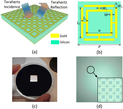
A schematic representation of the proposed dual-band terahertz metamaterial absorber is shown in Fig. 1(a). The absorber is based on a silicon substrate with a metal periodic array on the top, and a metal ground plane covering the whole bottom surface. The material of the metal is gold, with an electrical conductivity of 4.56 × 10⁷ S m−1. In addition, the silicon wafer grown on the (111) faces with both sides polished is in an intrinsic state and the resistivity is 2500–5000 Ohm cm. The thicknesses of the gold layers and the silicon substrate are t = 200 nm and d = 250 μm, respectively.The structure of the metamaterial unit cell is shown in Fig. 1(b). A square ring is set at the center of each unit cell and four T-shaped strips are loaded at the midpoints of the four sides of the square ring. The dimensions of the T-shaped strips are designed as follows: L1 = 2 μm, L2 = 24.1 μm, W1 = 1 μm, and W2 = 2 μm, while the width and outer side length of the square ring are W = 1.6 μm and a = 21 μm, respectively. On the upper surface of the silicon wafer, every pattern is perfectly aligned with a lattice constant of P = 33 μm. The size of the periodically patterned metamaterial structure is optimized to avoid undesired coupling.52,53
Fig. 1(c) shows a photograph of the fabricated metamaterial absorber prototype. Its overall size is 10 mm × 10 mm, containing 303 × 303 unit cells. As shown in Fig. 1(d), the image of the fabricated metamaterial periodic array obtained using a microscope indicates that the fabrication process is satisfactory without structural adhesions between the metal structures.
3 Simulation results and discussion
In this work, CST Microwave Studio software using a finite integration technique (FIT) frequency domain solver is employed to simulate the absorption and sensing characteristics of the proposed metamaterial absorber. In the simulations, the unit-cell periodic boundary condition is set for the proposed periodic array. The mesh size needs to satisfy the convergence and accuracy requirements. The incident plane waves are employed to illuminate the proposed absorber. The frequency dependent absorption rate A(ω) can be calculated as:| A(ω) = 1 − R(ω) − T(ω) | (1) |
| A(ω) = 1 − R(ω) = 1 − |S11(ω)|2. | (2) |
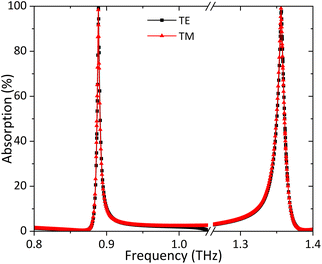
At the beginning, the absorption capabilities of the proposed metamaterial absorber were studied, including the performance of the conventional periodic array under normal transverse electric (TE) and transverse magnetic (TM) polarized incidences. The simulation results are shown in Fig. 2, which indicates that both the absorptions are over 99% at 0.89 and 1.36 THz under normal TE and TM polarized incident waves. The full widths at half maximum (FWHMs) of these two frequency bands are 4.4 and 11.2 GHz, which proves that a perfect dual-band absorber with low FWHMs is realized. Obviously, the two curves of absorption spectra are highly overlapping, which shows that the absorber has great polarization insensitivity. Another important index for absorbers is the quality factor (Q-factor), which can be expressed as
 | (3) |
| Ref. | Resonant frequency (THz) | Absorption rate (%) | FWHM (THz) | Q-Factor | Structure |
|---|---|---|---|---|---|
| 54 | 1.56 | >99 | 0.043 | 36.35 | Circular ring |
| 55 | 2.64 | >99 | 0.060 | 44 | Circular patch |
| 56 | 8.44 | 99 | 0.100 | 84.4 | Circular patch |
| 57 | 1.80 | 98 | 0.015 | 120 | Circular patch with square rings |
| 2.26 | 96 | 0.024 | 94 | ||
| This paper | 0.89 | >99 | 0.004 | 203.2 | Square ring with T-shaped strips |
| 1.36 | >99 | 0.011 | 121.4 |
The unit cell of proposed metamaterial absorber can be considered as an inductive-capacitive circuit model. According to the LC circuit element, the resonant frequency of the metamaterial absorber can be expressed as:
 | (4) |
In order to clarify the impedance matching condition, the basic equivalent circuit model of the present metamaterial absorber is shown in Fig. 3, where Z0 is the free space wave impedance, ZA is the overall impedance of the absorber, ZM is the impedance of the metamaterial structure, and Z1 stands for the impedance of the substrate layer backed with a gold ground, which can be considered as a short-circuited transmission line whose length is the thickness of the substrate. When the impedances ZA and Z0 are well matched with each other at the two operating frequencies, dual-band perfect absorption performance can be achieved. Some other relevant analyses and discussions can be seen as follows.
3.1 Analysis of the electric fields at resonant frequencies
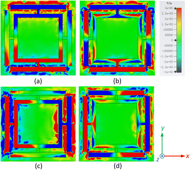
To explain the physical mechanism of the dual-frequency absorption properties of the suggested metamaterial absorber more clearly, the distributions of the z-component electric fields at 0.89 and 1.36 THz are shown in Fig. 4. Under normal TE polarized incidence, the electric field is mainly concentrated at the horizontal sides of the square metal ring and two horizontal T-shaped strips, as shown in Fig. 4(a), which is critical for generating the first resonant frequency at 0.89 THz. The high absorption rate at 0.89 THz is due to the joint effect of the square metal ring and T-shaped strips. Fig. 4(b) shows that the electric field is strongly enhanced along the two parallel metal strips. As can be seen, the two parallel metal strips will excite one more resonant mode, which is associated with the second resonant frequency at 1.36 THz.The distributions of the z-component electric fields of the proposed metamaterial absorber under normal TM polarized incidence at 0.89 THz and 1.36 THz are shown in Fig. 4(c) and (d), respectively. These distributions are just rotated 90° from those under TE polarized incidence, illustrating that the absorber has outstanding polarization-independent characteristics.
3.2 Analysis of parameter variations
Through the analysis of the electric field distributions of the metamaterial absorber, it is obviously found that the main factors of the two resonant frequencies are the outer side length of the square ring a, the lengths and widths of the T-shaped strips L1, L2, W1 and W2. Meanwhile, eqn (4) further proves that a change taking place in the values of these parameters can be reflected in the resonant frequencies. Thus, to figure out the effect of parameter variations, a series of analyses were carried out.As shown in Fig. 5(a), under normal TE polarization, when the parameter a increases from 20.2 to 21.8 μm, the first resonant frequency is blue-shifted slightly and the second one almost remains stable, which corresponds to the fact that the electric field concentrates around the square ring only at the lower resonant frequency. The two resonant frequencies are both blue-shifted with the parameter L1 changing from 1.6 to 2.4 μm in Fig. 5(b). As L2 increases from 22.6 to 24.6 μm, the first resonant frequency fluctuates slightly, while a blue-shift occurs at the second resonant frequency from 1.347 to 1.363 THz, which is shown in Fig. 5(c). Meanwhile, as shown in Fig. 5(d), the absorption spectra exhibit that the two resonant frequencies are both red-shifted with the width W1 increases from 0.2 to 1.8 μm. It can be seen in Fig. 5(e) that the two resonant frequencies are blue-shifted from 0.882 to 0.895 THz and from 1.349 to 1.363 THz, as the parameter W2 ranges from 1.5 to 2.5 μm.
Thus, the design process of the proposed dual-band metamaterial absorber can be divided into three steps. At the beginning, the side length of the square ring a was adjusted to determine the first absorption band at the anticipated resonant frequency. Then, the parameters of the T-shaped metal strips L1, L2, W1 and W2 were altered to shift the second absorption band to the required resonance frequency. Finally, a slight adjustment was made to the parameters in order to improve the absorption performance and modify the first frequency offset caused by the variations of T-shaped strips. Therefore, when a metamaterial structure needs to be constructed, it is necessary to figure out the relationship between the metal strip length and the operating wavelength. As for the specific metal structures, a few shapes could be considered, including but not limited to the square ring, the circular ring, the split ring resonator (SRR), the straight strip, and their combinations.
Through the analyses, it can be found that the variation trends of resonant frequencies are the same as the variation trend of parameter W1, which is different from the other parameters. The reason is that the increase of W1 creates a shorter current path on the T-shaped metal strips, leading to higher resonant frequencies. However, when the values of other parameters increase, the current path will be longer, which causes lower frequencies. As a result, the variation trends of resonant frequencies with shifting parameters are consistent with the principles of electromagnetism. Furthermore, the resonant frequency variations are maintained in a small range, which indicates that the proposed metamaterial absorber has good stability and the influence of fabrication accuracy on the absorption performance can be relatively low.
3.3 Analysis of the incident and polarization angles
The effect of different incident angles on the absorption rate has been investigated. As shown in Fig. 6(a) and (b), the resonant frequencies increase slightly with a stable absorption rate under both normal TE and TM polarized incidences when the incident angle θ rises from 0° to 30°. The corresponding variations of the Q-factors and their linear fits are shown in Fig. 6(c) and (d). The Q-factor linear fitting lines of the two operating frequency bands have the slopes of −0.11 and −0.66, respectively, under TE polarized incidence, while they are of −0.91 and −0.49 under TM polarized incidence.In addition, another index, polarization-independence, representing the stability of absorption rate with a varied incident polarization angle, is also of great importance for metamaterial absorbers. As shown in Fig. 6(e), the curves of the absorption spectra with the polarization angle φ varied from 0° to 90° are strongly overlapping, which demonstrates that the proposed metamaterial absorber is highly polarization-independent with the help of its outstanding central symmetry.
4 Measurement of absorption performance
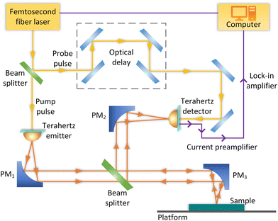
As shown in Fig. 7, a commercial terahertz TDS system with photoconductive antennas (TERAPULSE LX-K, TERAVIEW Co., Ltd) is used for measuring the absorption performance. A terahertz biased photoconductive emitter is illuminated using a femtosecond fiber laser with a pulse width of 100 fs and an 80 MHz repetition rate to produce terahertz pulses in this TDS system, whose operating frequency range is from 0.06 to 4 THz with a 5 GHz spectral resolution. In addition, two parabolic mirrors, PM1 and PM3, concentrate the terahertz pulses onto the absorber sample while the reflections are gathered by PM3 with a numerical aperture of 0.36 and then collected by PM2 onto a terahertz photoconductive detector to capture the transient response. Subsequently, a current preamplifier and a lock-in amplifier are used to measure the photocurrent outputted by the terahertz detector. Through a rapid Fourier transform, the observed signals are transformed from time-domain data to frequency-domain data. Due to the beam path in the TDS system, the incident angle remains at 15°. To prevent the accidental terahertz absorption by water vapor, all measurements are conducted in dry air while ambient temperature is controlled at 30 °C.After measuring an absorber using the system introduced above, two groups of data are obtained, including measurement data from the experimented sample and reference data representing the results from the system with the platform vacant. The absorption rate can be calculated using the abovementioned eqn (2). Additionally, to exclude undesirable environmental absorption, the reflection coefficient |S11(ω)|2 is expressed as a function of the measurement results normalized to the reference results, namely,
 | (5) |
 | (6) |
A series of samples of the proposed metamaterial absorber have been fabricated with parameter W2 shifting from 1.9 to 2.2 μm. The measured absorption rates under normal TE polarized incidence are shown in Fig. 8(a), illustrating that the first resonant frequency fluctuates slightly while the second resonant frequency decreases with the increase of W2. This phenomenon is consistent with the simulation. Meanwhile, as shown in Fig. 8(b), the measured absorption rates under normal TM polarized incident waves exhibit the same properties. Consequently, the fabricated absorbers have high sensitivity to the value of the geometric parameter. The second resonant frequency is slightly moved when comparing the results between simulation and measurement. The Q-factors of the measured results are lower than those of the simulated ones. The discrepancies between simulation and measurement may be caused by the following reasons. First, the simulation cannot well emulate the material characteristics of the silicon wafer employed in the fabrication process, including the crystal face and semiconductor types. Second, the thickness of the fabricated silicon wafer is 250 ± 25 μm, which was set as 250 μm in simulation. The inaccuracy of the substrate thickness will lead to a frequency deviation. Third, the standing waves inside the substrate were not considered during the simulation, which might cause inaccuracies around the second resonant frequency.
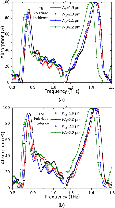 | ||
| Fig. 8 Measurement results of the fabricated dual-band metamaterial absorbers with different values of W2 under (a) normal TE polarized incidence and (b) normal TM polarized incidence. | ||
5 Sensing characteristics
To analyze the electromagnetic response of the present dual-band metamaterial absorber as a terahertz refractive index sensor, the absorption spectra were investigated with a layer of the analyte attached to the upper surface of the metamaterial absorber, as shown in the inset of Fig. 9(a). According to eqn (4), the inductance L and capacitance C in the effective LC circuit model are the primary determinants of the absorber's resonant frequency. When the absorber is employed as a refractive index sensor, the inductance L is still affected by the structure of the metamaterial. However, the capacitance C will be redefined as a new parameter Cn, which is related to the refractive index and thickness of the analyte. While a layer of analyte is coated on the absorber, the resonant frequency can be expressed as:60 | (7) |
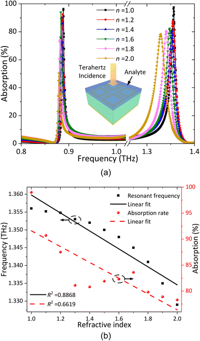 | ||
| Fig. 9 Sensing characteristics with the refractive index shifting from 1.0 to 2.0. (a) Absorption spectra and (b) further analysis of the second resonant frequency. | ||
Thus, the parameter Cn determined by the analyte plays a vital role in the sensing performance. In the simulation, the filling thickness of the analytes is designed as ta = 63 μm, which is capable of reflecting the sensing characteristics distinctly. In order to cover most biological and chemical specimens, including DNA, RNA, proteins, and amino acids, the refractive index of the analytes is set from 1.0 to 2.0.
The absorption spectra of the proposed metamaterial absorber with different refractive index analytes under normal TE polarized incidence are shown in Fig. 9(a). This illustrates that the first resonant frequency fluctuates slightly while a red-shift occurs for the second resonant frequency as the refractive index changes from 1.0 to 2.0. The details of the variations at the second frequency and their linear fits are shown in Fig. 9(b). On the one hand, the total red-shift of the second frequency is 37 GHz with an R2 value of 0.8868, and the fitting line function can be expressed as:
| f = −0.025 × n + 1.385. | (8) |
On the other hand, since the existence of analytes leads to the reduction of the reflection power, the absorption rate decreases from 99% to 78%. In addition, the frequency sensitivity is defined by the frequency variation per refractive index unit (RIU), calculated as:
 | (9) |
 | (10) |
Through calculations, the frequency sensitivity at the second resonant frequency of the proposed metamaterial absorber is 37 GHz RIU−1 and the FoM is 3.3. Comparisons between previous refractive index sensors and the proposed work are given in Table 2 for a clear insight into the sensing performance.
| Ref. | Resonant frequency (THz) | Sensitivity (GHz RIU−1) | FoM | Structure |
|---|---|---|---|---|
| 61 | 0.33 | 0.15 | 65.2 | Rhombus with triangular holes |
| 62 | 0.6 | 18 | 0.3 | I-shaped |
| 0.55 | 39 | 1.95 | Fano design | |
| 63 | 0.9 | 24.5 | 0.31 | Split square ring |
| 64 | 0.69 | 128.3 | 2.3 | Cross shaped |
| 0.81 | 113.3 | 1.98 | Complementary cross shaped | |
| This paper | 1.103 | 37 | 3.3 | Square ring with T-shaped strips |
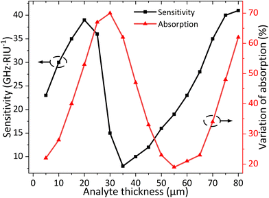
As shown in Fig. 10, in order to study the effect of the analyte thickness, the frequency sensitivity and variation of the absorption rate (when the refractive index shifts from 1.0 to 2.0) with the thickness increasing from 5 to 80 μm are simulated. The frequency sensitivity increases from 24 to 38 GHz RIU−1 and 7 to 42 GHz RIU−1 with the thickness ranging from 5 to 20 μm and 35 to 80 μm, respectively, while a decrease appears in the middle part. However, as the thickness of the analyte increases from 30 to 55 μm, the absorption rates under different refractive indices will not change dramatically. As a result, both the tendencies of the frequency sensitivity and absorption rate variation show the characteristics of a sinusoidal curve, which indicates that the proposed metamaterial absorber is also sensitive to the analyte thickness. It is observed from the analysis carried out above that the proposed metamaterial absorber has satisfactory sensing characteristics for practical applications.
6 Conclusions
In this paper, a dual-band terahertz metamaterial absorber with high Q-factors using a square metal ring with four T-shaped strips has been demonstrated. The absorption rates of both the two resonant frequencies are over 99% under TE and TM polarizations at 0.89 and 1.36 THz. The FWHMs of them are 4.4 and 11.2 GHz while the Q-factors are 202.3 and 121.4, respectively. Additionally, the absorption rate of the proposed absorber shows excellent stability with the increased incident angle from 0° to 30°. The polarization-independence of the metamaterial absorber is also impressive when the polarization angle rises from 0° to 90°. With the help of EBL and EBE technologies, the samples of the metamaterial absorber are prepared. Then, measurements are conducted using a terahertz TDS system, which proves that the fabricated metamaterial absorbers have good absorption properties. Furthermore, the sensing characteristics of the proposed metamaterial absorber has also been studied, which demonstrates that the absorber is sensitive to the refractive index and thickness of the analytes. As a result, our study offers a fresh option for designing high Q-factor dual-band metamaterial absorbers with refractive index sensing characteristics in terahertz frequencies.Author contributions
Dongxu Wang performed the simulation work, analysed the relative phenomena and drafted the manuscript; Kai-Da Xu created the concept and supervised the entire work; Siyuan Luo made the fabrication; and Yuqing Cui, Liuyang Zhang and Jianlei Cui carried out the experiments.Conflicts of interest
There are no conflicts to declare.Acknowledgements
This work was supported in part by the NSAF Joint Fund under Grant U2130102, in part by the State Key Laboratory of Advanced Optical Communication Systems Networks under Grant 2022GZKF020, in part by the State Key Laboratory of Precision Spectroscopy Open Research Program, and in part by the “Siyuan Scholar” Fellowship of XJTU.References
- S. Yang, K. Kim, H. Oh and J. Kang, NDT&E Int., 2013, 57, 45–51 CrossRef CAS.
- W. Taylo, Q. H. Abbasi, K. Dashtipour, S. Ansari, S. A. Shah, A. Khalid and M. A. Imran, Sensors, 2020, 20, 5665 CrossRef PubMed.
- Y. H. Tao, A. J. Fitzgerald and V. P. Wallace, Sensors, 2020, 20, 712 CrossRef PubMed.
- B. Wang, S. Zhong, T. Lee, K. S. Fancey and J. Mi, Adv. Mech. Eng., 2020, 12, 1–28 Search PubMed.
- X. Zhang, T. Chang, Z. Wang and H.-L. Cui, IEEE Access, 2020, 8, 144259–144276 Search PubMed.
- H. Du, J. Zhang, K. Guan, D. Niyato, H. Jiao, Z. Wang and T. Kürner, IEEE Trans. Commun., 2022, 70, 3575–3593 Search PubMed.
- E. Lacombe, C. B. Goncalves, C. Lucey, F. Gianesello, C. Durand, D. Gloria and G. Ducournau, IEEE Microw. Wireless Compon. Lett., 2018, 28, 362–364 Search PubMed.
- Y. Zhang, W. Yang, Q. Xue, J. Huang and W. Che, IEEE Trans. Antennas Propag., 2022, 70, 1989–1998 Search PubMed.
- Q. L. Zhang, B. J. Chen, K. F. Chan and C. H. Chan, IEEE Trans. Antennas Propag., 2021, 69, 4347–4358 Search PubMed.
- V. Krozer, et al. , IEEE Trans. Microwave Theory Tech., 2010, 58, 2027–2039 Search PubMed.
- S. Razavian and A. Babakhani, IEEE Trans. Microwave Theory Tech., 2021, 69, 4937–4950 Search PubMed.
- N. I. Landy, D. R. Smith and W. J. Padilla, Phys. Rev. Lett., 2008, 100, 207402 CrossRef CAS PubMed.
- W. Pan, X. Yu, J. Zhang and W. Zeng, IEEE J. Quantum Electron., 2017, 53, 1–6 Search PubMed.
- F. Chuhuan, S. Fan, S. Jian, L. Qi and Y. Hongbin, IEEE Photonics J., 2017, 9, 1–9 Search PubMed.
- Y. Cheng and J. Zhao, Phys. Scr., 2022, 97, 095508 CrossRef.
- H.-E. Su, J.-L. Li and L. Xia, IEEE Access, 2019, 7, 161255–161263 Search PubMed.
- Y. Cheng, J. Liu, F. Chen, H. Luo and X. Li, Phys. Lett. A, 2021, 402, 127345 CrossRef CAS.
- K. Iwaszczuk, A. C. Strikwerda, K. Fan, X. Zhang, R. D. Averitt and P. U. Jepsen, Opt. Express, 2021, 20, 635–643 CrossRef PubMed.
- Y. Wen, W. Ma, J. Bailey, G. Matmon and X. Yu, IEEE Trans. Terahertz Sci. Technol., 2015, 5, 406–411 Search PubMed.
- B. Wang, IEEE J. Sel. Top. Quantum Electron., 2017, 23, 1–7 Search PubMed.
- D. Hu, H. Wang and Q. Zhu, IEEE Photonics J., 2016, 8, 1–8 Search PubMed.
- D. B. Stojanović, G. Gligorić, P. P. Beličev, M. R. Belić and L. Hadžievski, IEEE J. Sel. Top. Quantum Electron., 2021, 27, 1–6 Search PubMed.
- K.-D. Xu, J. Li, A. Zhang and Q. Chen, Opt. Express, 2021, 28, 11482–11492 CrossRef PubMed.
- M. Huang, Y. Cheng, Z. Cheng, H. Chen, X. Mao and R. Gong, Materials, 2018, 11, 540 CrossRef PubMed.
- J. Zhao and Y. Cheng, Adv. Theory Simul., 2022, 2200520 CrossRef CAS.
- Z. Li, Y. Cheng, H. Luo, F. Chen and X. Li, J. Alloys Compd., 2022, 925, 166617 CrossRef CAS.
- Y. Cheng, Z. Li and Z. Cheng, Opt. Mater., 2021, 117, 111129 CrossRef CAS.
- F. Chen, Y. Cheng and H. Luo, IEEE Access, 2020, 8, 82981–82988 Search PubMed.
- Y. Cheng, Y. Qian, H. Luo, F. Chen and Z. Cheng, Phys. E, 2023, 146, 115527 CrossRef CAS.
- Y. Chen, X. Pan, Z. Bao, Y. Wang, Z.-D. Hu and J. Wang, IEEE Photonics J., 2021, 13, 1–12 Search PubMed.
- Z. Shen, S. Li, Y. Xu, W. Yin, L. Zhang and X. Chen, Phys. Rev. Appl., 2021, 16, 014066 CrossRef CAS.
- Y. Cheng, H. Zhao and C. Li, Opt. Mater., 2020, 109, 110369 CrossRef CAS.
- X. Shen, Y. Yang, Y. Zang, J. Gu, J. Han, W. Zhang and T. J. Cui, Appl. Phys. Lett., 2012, 101, 154102 CrossRef.
- Z. Cui, D. Zhu, L. Yue, H. Hu, S. Chen, X. Wang and Y. Wang, Opt. Express, 2019, 27, 22190–22197 CrossRef CAS PubMed.
- A. K. Singh, M. P. Abegaonkar and S. K. Koul, IEEE Trans. Electromagn. Compat., 2019, 61, 878–886 Search PubMed.
- G. Yao, F. Ling, J. Yue, C. Luo, J. Ji and J. Yao, Opt. Express, 2016, 24, 1518–1527 CrossRef CAS PubMed.
- Y. Zhang, C. Cen, C. Liang, Z. Yi, X. Chen, M. Li, Z. Zhou, Y. Tang, Y. Yi and G. Zhang, Results Phys., 2019, 14, 102422 CrossRef.
- Y. Wang, X. Zhang, T. Zhou, Y. Zhu, Z. Cui and K. Zhang, Front. Phys., 2021, 9, 749501 CrossRef.
- A. Mohanty, O. P. Acharya, B. Appasani, S. K. Mohapatra and M. S. Khan, IEEE Sens. J., 2021, 21, 22688–22694 Search PubMed.
- H. Singh, A. Gupta, R. S. Kaler, S. Singh and A. S. Gill, IEEE Sens. J., 2022, 22, 10524–10531 CAS.
- K. Shih, P. Pitchappa, M. Manjappa, C. P. Ho, R. Singh and C. Lee, J. Appl. Phys., 2017, 121, 023102 CrossRef.
- Z. Vafapour, IEEE Trans. Nanobiosci., 2019, 18, 622–627 Search PubMed.
- Y. Wang, D. Zhu, Z. Cui, L. Yue, X. Zhang, L. Hou, K. Zhang and H. Hu, IEEE Trans. Terahertz Sci. Technol., 2020, 10, 599–605 CAS.
- Y. Wang, Z. Cui, D. Zhu, X. Wang, S. Chen and P. Nie, Opt. Express, 2019, 27, 14133–14143 CrossRef CAS PubMed.
- M. Manjappa, A. Solanki, A. Kumar, T. C. Sum and R. Singh, Adv. Mater., 2019, 31, 1901455 CrossRef PubMed.
- G. Dayal, X. Y. Chin, C. Soci and R. Singh, Adv. Opt. Mater., 2017, 5, 1600559 CrossRef.
- L. Cong, Y. K. Srivastava, A. Solanki, T. C. Sum and R. Singh, ACS Photonics, 2017, 4, 1595–1601 CrossRef CAS.
- A. Kumar, M. Gupta, P. Pitchappa, T. C. Tan, U. Chattopadhyay, G. Ducournau, N. Wang, Y. Chong and R. Singh, Adv. Mater., 2022, 34, 2202370 CrossRef CAS PubMed.
- K. V. Sreekanth, Q. Ouyang, S. Sreejith, S. Zeng, W. Lishu, E. Ilker, W. Dong, M. ElKabbash, Y. Ting, C. T. Lim, M. Hinczewski, G. Strangi, K.-T. Yong, R. E. Simpson and R. Singh, Adv. Opt. Mater., 2019, 7, 1900081 CrossRef.
- K. V. Sreekanth, S. Han and R. Singh, Adv. Mater., 2018, 30, 1706696 CrossRef PubMed.
- K. V. Sreekanth, P. Mahalakshmi, S. Han, M. S. M. Rajan, P. K. Choudhury and R. Singh, Adv. Opt. Mater., 2019, 7, 1900680 CrossRef CAS.
- A. Bitzer, J. Wallauer, H. Helm, H. Merbold, T. Feurer and M. Walther, Opt. Express, 2009, 17, 22108–22113 CrossRef CAS PubMed.
- J. Wallauer, A. Bitzer, S. Waselikowski and M. Walther, Opt. Express, 2011, 19, 17283–17292 CrossRef CAS PubMed.
- J. Yu, T. Lang and H. Chen, Photonics, 2021, 8, 164 CrossRef CAS.
- S. Banerjee, U. Nath, P. Dutta, A. V. Jha, B. Appasani and N. Bizon, Inventions, 2021, 6, 78 CrossRef.
- J. Wang, et al., Ultrahigh-Q and Polarization-Independent Terahertz Metamaterial Perfect Absorber, Plasmonics, 2020, 15, 1943–1947 CrossRef CAS.
- M. Janneh, A. De Marcellis, E. Palange, A. T. Tenggara and D. Byun, Opt. Commun., 2018, 416, 152–159 CrossRef CAS.
- B. X. Wang, X. Zhai, G. Z. Wang, W. Q. Huang and L. L. Wang, IEEE Photonics J., 2015, 7, 4600108 Search PubMed.
- A. Ebrahimi, R. T. Ako, W. S. L. Lee, M. Bhaskaran, S. Sriram and W. Withayachumnankul, IEEE Trans. Terahertz Sci. Technol., 2020, 10, 204–211 CAS.
- J. F. O'Hara, R. Singh, I. Brener, E. Smirnova, J. G. Han, A. J. Taylor and W. L. Zhang, Opt. Express, 2008, 16, 1786–1795 CrossRef PubMed.
- A. Kumar, M. Gupta, P. Pitchappa, Y. J. Tan, N. Wang and R. Singh, Appl. Phys. Lett., 2022, 121, 011101 CrossRef CAS.
- M. Gupta and R. Singh, Adv. Opt. Mater., 2020, 8, 1902025 CrossRef CAS.
- T. C. Tan, Y. K. Srivastava, R. T. Ako, W. Wang, M. Bhaskaran, S. Sriram, I. Al-Naib, E. Plum and R. Singh, Adv. Mater., 2021, 33, 2100836 CrossRef CAS PubMed.
- L. Cong, S. Tan, R. Yahiaoui, F. Yan, W. Zhang and R. Singh, Appl. Phys. Lett., 2015, 106, 0331107 CrossRef.
| This journal is © The Royal Society of Chemistry 2023 |

