 Open Access Article
Single-molecule functionality in electronic components based on orbital resonances
Mickael L.
Perrin
 *ab,
Rienk
Eelkema
 c,
Jos
Thijssen
a,
Ferdinand C.
Grozema
 c and
Herre S. J.
van der Zant
 *a
*a
aKavli Institute of Nanoscience, Delft University of Technology, Lorentzweg 1, 2628 CJ Delft, The Netherlands. E-mail: H.S.J.vanderZant@tudelft.nl
bSwiss Federal Laboratories for Materials Science and Technology, Überlandstrasse 129, 8600 Dübendorf, Switzerland. E-mail: Mickael.Perrin@empa.ch
cDepartment of Chemical Engineering, Delft University of Technology, van der Maasweg de 9, 2629 HZ Delft, The Netherlands
First published on 1st June 2020
Abstract
In recent years, a wide range of single-molecule devices has been realized, enabled by technological advances combined with the versatility offered by synthetic chemistry. In particular, single-molecule diodes have attracted significant attention with an ongoing effort to increase the rectification ratio between the forward and reverse current. Various mechanisms have been investigated to improve rectification, either based on molecule-intrinsic properties or by engineering the coupling of the molecule to the electrodes. In this perspective, we first provide an overview of the current experimental approaches reported in literature to achieve rectification at the single-molecule level. We then proceed with our recent efforts in this direction, exploiting the internal structure of multi-site molecules, yielding the highest rectification ratio based on a molecule-intrinsic mechanism. We introduce the theoretical framework for multi-site molecules and infer general design guidelines from this. Based on these guidelines, a series of two-site molecules have been developed and integrated into devices. Using two- and three-terminal mechanically controllable break junction measurements, we show that depending on the on-site energies, which are tunable by chemical design, the devices either exhibit pronounced negative differential conductance, or behave as highly-efficient rectifiers. Finally, we propose a design of a single-molecule diode with a theoretical rectification ratio exceeding a million.
1 Introduction
Ever since the dream of single-molecule electronics has been introduced,1 the research community has explored a large range of phenomena at the single-molecule level based on the charge and spin degree of freedom,2–11 such as switching,12,13 thermoelectricity,14,15 spin-crossover,16,17 Kondo effect,18–21 and mechanical tunability20,22–26 with as central theme the link between chemical structure and device functionality.6,27,28 The ultimate goal is the on-demand tunability of the orbital structure of a molecule, to enable the engineering of single-molecule device functionalities. To date, a large range of such functionalities have been realized experimentally, with molecules being employed as transistors,3,18,29–31 diodes,32–39 resonant-tunneling diodes,40 switches,12,13,41,42 light-emitters,43 photoresponsive devices,44 memory elements,45 thermoelectric power generators,14,15,46 potentiometers47 and strain-sensors.26 Common approaches in the design of single-molecule devices are the engineering of the coupling to the electrodes via various anchoring groups,48–52 and controlling the level alignment of the molecular orbitals closest to the Fermi energy of the contacts, either by chemical means53 or using an electrostatic gate (solid-state3,18–21,29–31 or an electrochemical54–57), and the exploitation of quantum effects such as destructive interference.56–59In particular, diodes have attracted attention,32–39 in part due to their ubiquitous role in modern semiconducting chips for current rectification, as well as their straightforward working principles. Before discussing the different mechanisms of molecular rectification, we introduce the central diode characteristics that can be used to compare then: an important figure of merit for diodes is the current ratio between both bias polarities |I(V)/I(−V)|, also called the rectification ratio (RR). We will refer to the bias voltage at which this ratio is obtained as the operating voltage.
2 Diode mechanism
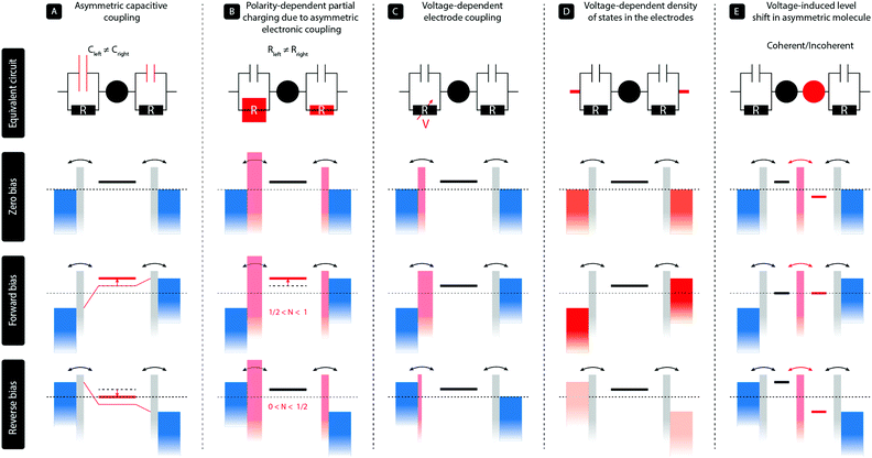
In a two-terminal junction, a single molecule is attached to two metal electrodes through anchoring groups that have a specific binding affinity with the metal, for instance, a thiol group connected to gold. The discrete energy levels of the molecule then interact with the continuous density of states in the electrodes, and due to this hybridization, electrons can tunnel on and off the molecule. This results in a finite dwell time of the electron on the molecule, and therefore an energy broadening of the molecular levels. In a simplified picture, such a single-molecule junction can be represented by a single level coupled to the two metallic leads via a capacitor and a resistor in parallel, as illustrated in the top panels (A–D) of Fig. 1. The ratio of the two capacitors controls the voltage division across the two barriers; no voltage falls across the level itself. The two resistors, on the other hand, represent the electronic coupling between the molecule and the leads and thus describe the tunneling rates of charge to and from the molecule. In this model, diode-like behavior can be obtained by the following main mechanisms:(A) In the most simple, purely electrostatic case, an asymmetry in the two capacitors60 leads to a voltage drop across the junction that is unequally distributed across the two electrode/molecule interfaces. This results in an effective shift of the molecular level with applied bias voltage and hence a dissimilar level position for opposite bias polarities. This mechanism can be achieved with asymmetric anchoring groups or by using dissimilar electrode areas.35
(B) In the case of asymmetric tunnel barriers,61 the tunneling rates on and off the molecule are dissimilar for opposite bias polarities. In the Landauer picture including partial charging, the energy of the level is given by ε = ε0 + U(〈N〉 − N0), where ε0 and N0 are the level position and occupation at zero bias, respectively, and U the charging energy. As 〈N〉 depends on the bias voltage and polarity, so does the level position, resulting in rectification. We note that this partial charging also leads to an additional level broadening. This mechanism can, for instance, be realized by employing anchoring groups with a different orbital overlap with the electrodes. We stress that asymmetric tunneling barriers without partial charge transfer do not result in rectification.
(C) For particular types of asymmetric molecules with, for instance, on the left side a para-connected moiety and on the right side a meta-connected moiety, the response of the molecular orbitals to the electric field generated by the bias voltages can be asymmetric.62 In other words, due to quantum interference effects, a positive bias across the molecular junction has a different effect on the charge density on the molecule than the same bias voltage with opposite polarity. As the electronic coupling of a molecule to each electrode is proportional to the square of the wave function on the anchoring groups, this scenario may lead to a voltage-dependent electronic coupling. These voltage-dependent tunneling barriers result, in turn, in an enhanced current for a particular bias direction and hence rectification.
(D) For dissimilar electrode materials, the density of states may differ per electrode and may even be voltage dependent (illustrated by the different shades of red), such as is, for instance, the case in graphite63 or highly n-doped semiconductors.39 In the latter case, the semiconducting electrode is in charge accumulate at the electrode surface for one bias polarity and charges can easily tunnel through the molecule, but the semiconductor is depleted in the opposite case and transport is blocked.
The rectification mechanisms A–D occur in a single molecule with a single level dominating transport. However, rectification can also occur when more than one level is involved in transport, as in the case for molecules consisting of two sites in series. In Fig. 1 this mechanism is denoted by E.
(E) The situation is analogous to semiconducting pn-junctions and comprises a conjugated molecule with two unequal π-systems (usually a donor and an acceptor) connected in a rod-like fashion. Due to the asymmetry in the electron density on both halves, the orbitals located on each of them have different energies. The lack of internal alignment of the energies levels leads to a suppressed current at zero bias. Under the influence of an applied bias voltage, the energy levels located on each of the halves shift and align only for the forward bias direction, while they are pulled apart in the opposite case. This results in a polarity-dependent current and hence rectification. We note that for a large inter-site coupling, the molecule effectively behaves as a single level. Finally, this mechanism can either occur in the coherent transport regime, in which case transport is resonant across the molecule, or in the incoherent regime, requiring the presence of vibrational modes. In the latter case, vibrationally excited states are required and charge flows according to the Franck–Condon principle.1
We finally note that we have restricted ourselves to mechanisms that occur at the single-molecule level and have been verified experimentally as such. We also note that in some systems, several of these mechanisms can be at play at the same time,34,63 and disentangling them may not always straightforward. This is, particularly, true for mechanisms A and B, as the capacitive and electronic coupling of the molecule to the electrodes are related one to another.
The first theoretically proposed single-molecule diode in 19741 was based on the incoherent version of the two-site mechanism (E). The first experimental demonstration of single-molecule rectification32 was realized in 2005 and was based on the coherent version of this mechanism. In that study, an RR of about 10 was obtained at 1.5 V. Despite many attempts, it took almost a decade for the first single-molecule diode with a rectification ratio reaching 100 to be observed.36 Here, the junction was based on a molecule with an asymmetric electronic and capacitive coupling to the electrodes (A & B). In the same year, a rectification ratio of 200 was reached by using a symmetric molecule in an ionic solution in combination with asymmetric electrode areas (A) to generate an asymmetric voltage drop at the molecule/electrode interfaces.35 Several studies have followed since, with the highest RR reported to date as high as 4000, using a symmetric molecule in combination with asymmetric electrode materials (gold on one side and doped silicon on the other, mechanism D). Table 1 provides an overview of the experimental single-molecule rectifiers realized to date, including the reported rectification ratio and operating voltages. We note that, apart from at the single-molecule level, rectifiers have been realized in self-assembled monolayers,76–78 with rectification ratios reaching as high as 100![[thin space (1/6-em)]](https://www.rsc.org/images/entities/char_2009.gif) 000.79 The highest experimental single-molecule value based on an intrinsic molecular mechanism is 620, realized based on mechanism E, exploiting resonant transport between two weakly coupled sites.38
000.79 The highest experimental single-molecule value based on an intrinsic molecular mechanism is 620, realized based on mechanism E, exploiting resonant transport between two weakly coupled sites.38
| Reference | RR | Operating voltage (V) | Mechanism | Additional info |
|---|---|---|---|---|
| Elbing et al. 200532 | 10 | 1.5 | E | First single-molecule diode |
| Morales et al. 200564 | 9 | 1.5 | E | Inversion by protonation |
| Diez-Perez et al. 200933 | 10 | 1.5 | E | Controlled orientation |
| Hihath et al. 201165 | 3 | 1.5 | E | Combined with IETS |
| Wang et al. 201166 | 3.5 | 2.0 | E | Single or few molecules |
| Lörtscher et al. 201234 | 11 | 1.5 | A/B/E | |
| Batra et al. 201367 | 3.5 | 0.85 | A/B | Tunable by chemical design |
| Kim et al. 201463 | 3.5 | 0.5 | A/D | Graphite/gold electrodes |
| Batra et al. 201462 | 2 | 0.85 | C | Enabled by quantum interference |
| Wang et al. 201468 | 5.5 | 1.0 | A/B | |
| Zoldan et al. 201569 | 8.3 | 0.75 | A/B | |
| Fujii et al. 201570 | 10 | 0.1 | E | Aromatic stack of molecules |
| Sherif et al. 201536 | 100 | 1.5 | A/B | Distance tunable rectification ratio |
| Capozzi et al. 201535 | 200 | 0.37 | A | Symmetric molecule, in liquid |
| Guo et al. 201637 | 15 | 1.1 | C | DNA-based |
| Meany et al. 201671 | 6 | 1.5 | E | |
| Koepf et al. 201672 | 2 | 0.8 | A/B | |
| Perrin et al. 201638 | 620 | 1.2 | E | Gate tunable |
| Aragones et al. 201739 | 4000 | 1.5 | D | Silicon/gold electrodes |
| Yamada et al. 201873 | 8 | 1.3 | E | Distance tunable rectification ratio |
| Fujii et al. 201974 | 2 | 1.5 | E | |
| Handayani et al. 201975 | 14 | 1.5 | E | Three sites |
In this Perspective, we will review in detail our approach with molecules consisting of conjugated sites connected via non-conjugated linkers. We will show that the weak coupling between the sites is crucial, as it can lead to the formation of multiple (distinct) sites in series, the energy of which can be tuned by external electric fields, i.e., by the Stark effect. We will demonstrate how this effect enables adjustment of the internal level structure, giving rise to phenomena such as negative differential conductance and rectification. These two device behaviors are key in modern electronic circuits as they constitute the working principle of resonant tunneling diodes80,81 and diodes,82,83 respectively.
3 N-Site model
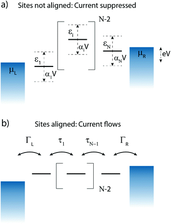
Charge transport through molecules consisting of N conjugated parts connected by saturated linkers (schematically illustrated in Fig. 2) can be described using a model consisting of N sites in series (i = 1,…,N), each of them characterized by an on-site energy εi. The saturated linkers between the sites result in the sites being weakly coupled to each other with an inter-site coupling strength τi. We first consider a two-site model, in which each site is coupled to only one of the electrodes (left or right) by a coupling strength ΓL,R. The alignment of the individual sites can be changed either by chemical substitution. Upon application of an applied bias voltage and as a result of the weak coupling between the sites, part of the voltage drops inside the molecule by an amount αi·V, providing a second way of influencing this alignment. This internal voltage drop, resulting in a bias-dependent alignment, is crucial to achieving bias-dependent transmissions. Finally, applying a non-uniform gate field can also introduce an asymmetry in the on-site energies. However, we will not explore this scenario further as experimentally this is extremely challenging to realize and to control.In the following, we will show that depending on the model parameters, different types of devices can be designed using molecules that behave as two sites in series, including a resonant tunneling diode and a rectifier. For two sites in series, the schematic Hamiltonian, which includes the application of a bias voltage, is given by
 | (1) |
 and
and  . Δ is the energy splitting between the two orbitals in the presence of a bias voltage, and is given by
 | (2) |
 , where η = eV·(α1 + α2) + (ε1 − ε2). As
  and τ > 0, this gives Δ ≥ η and both indices are positive. Therefore, there are no nodes present in between the sites and this orbital has a bonding character. The highest orbital, on the other hand (with energy επ*) has an eigenvector
  . Now, the two indices have opposite sign, yielding one node in between the sites and an antibonding orbital.
To describe charge transport through the molecule, we now symmetrically couple the left and right sites to the corresponding electrodes in the wide-band limit,84,85 thereby neglecting the real part of the self-energy matrices and assuming the electronic coupling to be energy independent:
 | (3) |
![[scr T, script letter T]](https://www.rsc.org/images/entities/char_e533.gif) (ε) = Tr{ΓLGr(ε)ΓRGa(ε)}, (ε) = Tr{ΓLGr(ε)ΓRGa(ε)}, | (4) |
 | (5) |
 | (6) |
 | (7) |
 and
and  , and assuming EF = 0 eV, we obtain
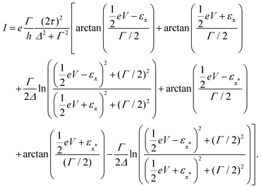 | (8) |
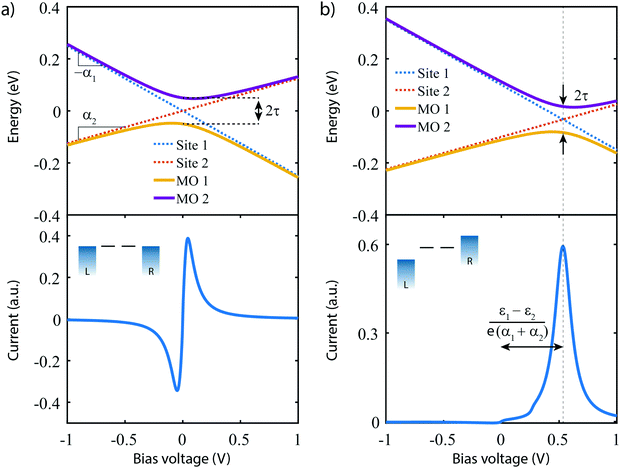
The lower panel of Fig. 3a presents a current–voltage characteristic (IV) calculated using eqn (8), with the model parameters provided in the figure caption. At zero bias, the IV has a high conductance as the sites are on resonance. When increasing the bias voltage, two competing effects occur. First, the increase in voltage leads to an increase in current. On the other hand, the bias also pulls the sites apart, thereby reducing the transmission through the system (and hence the conductance). For low bias, the first mechanism dominates and the current increases with bias. For bias voltages above 40 meV, however, the second effect starts to dominate. This leads to a strong negative differential conductance (NDC); for high bias voltages the sites are far apart and the current decays to zero.
In the more general case when ε1 ≠ ε2, the system is asymmetric and the bias voltage at which the two site energies meet is shifted, and equal to  . This scenario is depicted in the upper panel of Fig. 3b. Again, far away from Vcross, the MOs converge towards the site energies, which move in energy with α1 and −α2. The lower panel of Fig. 3b presents the calculated IV: at zero bias voltage, the sites are misaligned, and the current is low. For positive voltages, the current initially slowly increases, until a sharp increase occurs and a peak is reached at Vcross = 0.533 eV where the energies of the sites are equal. For even higher biases, the sites are pulled off-resonance again, leading to a decreased current for increasing bias voltages, and hence NDC. For negative bias voltages, the sites are pulled further apart from the start and the current remains low. This system, therefore, behaves as a rectifier: it blocks current for one bias polarity, while it allows it to flow for the opposite one. For the parameters used in the figure, the RR reaches a maximum of 318 at Vcross = 0.533 V. It is important to note that the mechanism described here exists in the fully coherent limit, not requiring incoherent processes.
In conclusion, a system consisting of two sites in series either behaves as a resonant tunneling diode, exhibiting NDC, or as a diode; the distinguishing parameter being the (a)symmetry of the two on-site energies.
4 Model parameter dependence: optimizing rectification of current in a diode
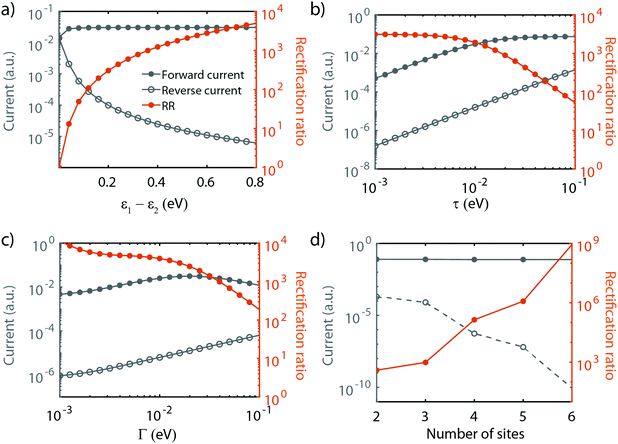
As shown in the previous section, transport through molecules consisting of conjugated parts connected by saturated linkers can either exhibit NDC or rectification, depending on the model parameters αi and εi. In this section, we discuss in more detail the effect of the parameters (including Γ and τ) on the RR, and in particular how each of them can be tuned to enhance it.We start with the role of the on-site energies. As mentioned previously, when the sites are aligned at zero bias, the molecule behaves as a resonant tunneling diode. When introducing an asymmetry in the site energies, these meet at a finite bias voltage (which scales linearly with the energy splitting) for one particular polarity, and rectification occurs. Fig. 4a presents the dependence of the rectification ratio and current on the energy splitting between the sites (ε1 − ε2). Note, that for ε1 − ε2 = 0, RR = 1. The RR strongly depends on the energy splitting, with the largest splitting yielding the better diode performance. This can be understood by considering the forward and reverse current. When increasing the on-site energy splitting, a larger bias voltage is needed to align the sites. At the same time, this also implies that at reverse bias the sites are increasingly further apart. This results in a lower leakage current, which, combined with the fact that the forward current (with the sites aligned) remains largely unaffected when increasing the energy difference between ε1 and ε2, yields an increase in RR.
The effect of τ and Γ can intuitively be understood as follows. Both parameters affect the electron tunneling rates, and therefore both the electron lifetimes on the molecule and the energy broadening of the sites. The forward current is determined by resonant transport, while the reverse current is a result of the overlap of the tails of the two sites. The reverse current is therefore expected to be more sensitive to the electron lifetimes than the forward current: reducing the level broadening, therefore, enhances the rectification ratio. Fig. 4b depicts the influence of the inter-site coupling τ on the RR. With the forward and reverse current following the previously described behavior, this results in an increase in RR with decreasing τ, in particular for τ > 5 × 10⁻³ meV, albeit at the cost of a lower peak current. A similar trend is observed for the dependence on Γ, as shown in Fig. 4c.
Last, but not least, the number of sites also plays a crucial role in the diode performance, as illustrated in Fig. 4d. In forward bias, when all the sites are aligned, transport is resonant, and increasing the number of sites only marginally affects the forward current. In the reverse bias mode, on the other hand, the current depends on the overlap of the tails of the lifetime broadened sites. Upon an increase in the number of sites, the ‘cost’ for an electron to go from one site to the next needs to be paid over and over again at each jump, resulting in an exponential decrease of the reverse current. This strong decrease in the reverse current leads to a dramatic increase in RR. However, this comes at a price. As more electrons are present on the molecule, other orbitals are more closely located, potentially leading to the participation of these additional orbitals in transport. Moreover, from an experimental point of view, more sites imply a longer molecule. This may lead to a reduced solubility, surface mobility and/or increased mechanical degrees of freedom. These three effects may result in a low yield of molecular junction formation.
We note that the parameter α does not influence the maximum rectification ratio. It merely affects the voltage at which this maximum will be achieved. In conclusion, we found that the RR can be enhanced as summarized in Table 2.
| Parameter | Optimize | Drawback |
|---|---|---|
| ε 1 − ε2 | Increase | Larger operating voltage |
| τ | Decrease | Lower peak current |
| Γ | Decrease | Lower peak current |
| Number of sites | Increase | Parasitic orbital contributions and larger molecule |
5 Chemical design guidelines
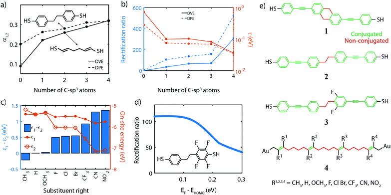
In this section, based on the parameter optimization discussed previously, we will present guidelines for designing efficient single-molecule diodes. To make a link between the model parameters and the chemical structure of molecules, molecular orbital energies were obtained from density functional theory (DFT) calculations, performed using the Amsterdam Density Functional (ADF) quantum chemistry package with the GGA PBE exchange–correlation functional and the triple-ζ plus polarization (TZP) basis-set.87–89 Transmissions were then calculated by coupling the 3pz-orbitals of the anchoring sulfur atoms to wide-band electrodes with a coupling strength of 100 meV. We note that this coupling strength determines the injection of the electrons into in the sulfur atoms, and is different from the coupling strength mentioned earlier for the N-site model that describes the coupling between the electrode and an orbital that is delocalized over an entire (conjugated) site. Although the two are related, they cannot be directly compared to another. A bias voltage was applied to the molecule by introducing a uniform electric field along the axis connecting the sulfur atoms. The model parameters were obtained by fitting the two-site Hamiltonian to the DFT-based calculations.Single-molecule diodes based on two sites connected in series need to fulfill a few requirements. First of all, the molecule should possess two conjugated parts, which are weakly coupled to each other. The conjugated parts can, for example, be phenyl rings or vinylene groups. For the two-site model to be valid, the two molecular orbitals making them up should be well separated in energy from other orbitals. These additional orbitals may, for instance, be the LUMO and/or HOMO−2, in the case where the HOMO and HOMO−1 are the ones under consideration. These additional orbitals could contribute significantly to the current in the reverse bias mode and this parasitic contribution deteriorates the rectification ratio. As the density of orbitals scales with the number of electrons in the system, key to reducing undesirable orbital contributions is to minimize the total number of electrons on the molecule, and in particular of each site. For two-site molecules, this effect is not significant yet, and both single phenyl and vinylene units can be used as sites. For more sites in series, however, vinylene becomes the better choice (see Section 10).
The second consideration is that the energy of the sites located on either half of the molecules needs to be different from another and tuneable by the bias voltage. The potential profile inside a molecular junction has been a topic of debate,90 as in an ideally conducting molecule all voltage should drop across the molecule/electrode interfaces due to the dielectric screening of the molecule.91 However, molecules are not perfect conductors, and as the molecular conductance and molecular polarizability are intimately linked,91 the bias field is only partially screened and a portion of the voltages gradually drops across the molecule as well. More substantial voltage drops can be realized by the introduction of weak links in conjugated molecules.92
Examples to realize this weak coupling include twisted biphenyl moieties27,55 or saturated (sp3) carbon chains.1 Twisted phenyl rings have the drawback that the strength of the link strongly depends on the square of the torsion angle between them, especially in the weak coupling limit when the sites are oriented at an angle close to 90°. Therefore, we will focus on saturated carbon (C-sp3) chains.
Fig. 5a presents the dependence of the fraction of the voltage drop between two neighboring sites, on the number of C-sp3 atoms in the bridge for two prototypical molecules, diphenyl-ethane (DPE) and divinylene-ethane (DVE), as shown in the insets. The plot shows that the voltage drops α1,2 can be increased by adding C-atoms to the bridge. It also reveals that DPE intrinsically has a larger α for short chains. This effect is attributed to the non-planar nature of the molecule, which results in a twist in the middle and hence a weaker coupling (larger α) between adjacent sites and hence a larger voltage drop.
The third consideration is that the inter-site coupling τ should be weak. This requirement makes that the parameters τ and α are linked one to another, both requiring a weak electronic link in the molecule. Indeed, Fig. 5b shows that increasing the number of sp3-C in the DVE and DPE molecule also significantly reduces the inter-site coupling τ. Combined with an increased α, this leads to a significant increase in the RR. However, one should not forget about the contribution of the σ-orbitals to charge transport. In the discussion of the model, we focus on the contribution of the π-orbitals as these ones dominate transport. Even though the σ-orbitals only have a small contribution, they may become important in the reverse bias direction when the π-orbitals are suppressed. Therefore, the weak inter-site coupling should not only decouple the π-orbitals, but also suppress the contribution of the σ orbitals. This is achieved by increasing the number of C-sp3 atoms in the bridge.
We would like to stress the importance of this weak coupling. Experimental studies have been performed on single-molecule diodes using similar organic molecules,33,34 in which no distinct weak coupling was present. Low RR's were reported, which we attribute to the inter-site coupling being too strong, even for twisted phenyl rings.
Fourth, for rectification to occur, the ability to control the site energies is a prerequisite, as it is needed for introducing the asymmetry at zero bias and aligning the sites at a finite bias voltage. This can be achieved by chemical substitution of all hydrogen atoms of the different sites by electronegative or electropositive groups, such as F, OH, OCH3, CH3, CF3, NO2 and CN. To investigate this effect, we used the DPE molecule and chose the right site for this substitution (see inset of Fig. 5d for the F-substitute version); for each substituent, DFT calculations were performed as described previously. The on-site energies for different substitutions are presented in Fig. 5c. The plot shows that the energy of the unsubstituted site (ε1, solid dots) remains approximately constant for all groups. The small mutual influence of the left on the right site and vice versa is attributed to the weak coupling between the sites and becomes even smaller with more sp3 C-atoms in the bridge. The energy of the right site (ε2, open dots), on the other hand, varies by more than 1.5 eV, between the electropositive methyl group (CH3) and the highly electronegative nitro (NO2). The bar plot shows that the energy splitting ε1 − ε2, which steadily increases from −0.2 eV to 1.4 eV, resulting in a large range of tuning of the sites.
We note that an asymmetry in the on-site energies of the two-site system can also be achieved by using a different anchoring group for each half of the molecule.92 However, that approach suffers from two disadvantages. First, the coupling strength and on-site energy cannot be independently adjusted. As discussed in Section 4, the tunability of each model parameter is critical to achieving high-performance diodes. Second, by relying on the anchoring groups to shift the energy of the sites, the approach is limited to molecules consisting of two sites only, and hence this principle cannot be easily extended to multi-site systems containing more than 2 sites.
Fifth, in the calculations, we assume that at zero bias (V = 0) the HOMO is on resonance with the Fermi energy. Fig. 5d shows the RR for a two-site model when this is not the case, as the Fermi energy lies above the HOMO. The plot shows that the highest RR is obtained when being on resonance, and decreases for increasing misalignment. This can be understood by considering the limit in which the HOMO is far away from the Fermi energy. In that case, the two sites are much further away from the Fermi energy than they are from each other, eventually converging to a symmetric situation in which the RR decays to unity. Experimentally, having the HOMO close to the Fermi energy may require the presence of an electrochemical/electrostatic gate, and also puts constraints on the anchoring groups. These groups should promote hole transport and bring the HOMO as close as possible to the Fermi energy of the electrodes, in which case thiols and direct carbon-gold bond (sp3 C-Au) seem better suited than for instance amines or methyl sulfides.51
Finally, we point out that the calculations assume wide-band limit electrodes that inject current directly into the 3pz orbitals of the sulfur for the thiol-ended molecule, and the 6s orbital of the Csp3–Au terminated molecules. This assumption implies that charge transfer between the molecule and the electrodes, as well as image-charge effects25,93,94 present due to the metallic electrodes are neglected. Moreover, the model does not include the role of temperature and the environment, which both lead to decoherence and inelastic-dissipative effects, and have been reported to reduce the rectification ratio by a factor of 2–4.95
Following these guidelines, and keeping in mind chemical feasibility, we proposed several molecular resonant tunneling diodes and diode, of which the chemical structures are shown in Fig. 5e. Molecule 1 and 2 have been synthesized96,97 with the aim to test the symmetric two-site model. For the asymmetric model, 3 was designed and synthesized, a modified version of molecule 2.97
In the next sections, we present calculations and measurements involving multi-site molecules in detail. We start with the two-site case using molecules 1–3. After experimental verification that charge transport through this class of molecules can indeed be described by the two-site model, we continue with molecule 4. This molecule constitutes a highly optimized diode, with four ethylene sites, and butane bridges for promoting a weak coupling. This molecule will be discussed theoretically in Section 10.
6 DFT calculations on the symmetric two-site DPE molecule
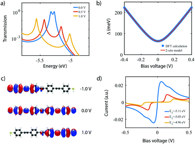
To investigate the charge transport properties of molecule 2, DFT + NEGF calculations were performed as described previously. Fig. 6a presents the transmission through the molecule in the presence of an applied bias voltage. At zero bias, a nearly-degenerate peak is observed around −5.3 eV, which originates from the closely located HOMO and HOMO−1. Upon application of a bias voltage, a Stark shift causes the orbitals to be pulled apart leading to a suppression of the transmission. Fig. 6b shows the energy splitting of the two orbitals (Δ) as a function of the bias voltage. The coupling causes the two aligned sites to be split by 64 meV at zero bias. The DFT values are fitted to the eigenvalues of the two-site Hamiltonian (eqn (1), solid orange line in Fig. 6b), which reproduces the values remarkably well. From this fit, the model parameters τ and α can be extracted.Fig. 6c presents the isosurface of the HOMO for different bias voltages. At zero bias, this orbital is delocalized across the entire molecule, extending from one sulfur atom to the other. In the presence of an electric field, however, the orbital is pulled to one side of the molecule: to the left for negative bias, and to the right for positive bias. This is consistent with the eigenstates of the two-site model. This localization is caused by the misalignment in energy of the two molecular halves, and is the main cause for the decrease in transmission observed in Fig. 6a. The current, shown in Fig. 6d, is calculated by integrating the transmission (see eqn (7)), assuming a temperature of T = 0. When choosing the Fermi energy to be on resonance with the HOMO (EF = −5.27 eV), a distinct NDC feature is observed. When moving the Fermi energy away from the HOMO, the aligned sites are not present in the bias window at zero bias and the current is blocked. A finite bias is then required for the sites to enter the bias window, and the NDC peak moves towards higher bias voltages. For an upward shift of the Fermi energy, the NDC peak, therefore, moves towards higher bias voltages, and the region of blocked current increases.
In the following, our goal is to obtain a quantum chemistry description of the sites in terms of the atomic orbitals used in our DFT calculations. To do so, we elaborate on the distinction between molecular orbitals (MO) versus localized molecular orbitals (LMO). We then apply this principle to the symmetric 2-site molecule DPE (3), and further on in this Perspective to the asymmetrically substituted 4-site molecule C4-tetraene (4).
Generally speaking, the MOs are linear combinations of the basis functions describing the system. They are obtained by diagonalizing the Hamiltonian of the system, with the eigenvectors providing the orbital shape and the eigenvalues the orbital energy. This holds both for our N-site model as well as for DFT calculations. For the N-site model, each site is described by a single basis function, and hence the number of MOs is equal to the number of sites N. In our N-site model, the wave function of the MOs (Φmodeln, n = 1,…,N) is therefore given by
 | (9) |
 | (10) |
In a molecule behaving according to the N-site model, however, only N π-orbitals contribute to transport. For convenience, we define the set of dominant π-orbitals as Π, with the individual orbitals labeled p (p = Π[1,…,N]). Physically speaking, both ΦDFTp and Φmodeln represent the same MOs and are equivalent. One can therefore combine eqn (9) and (10) and obtain
 | (11) |
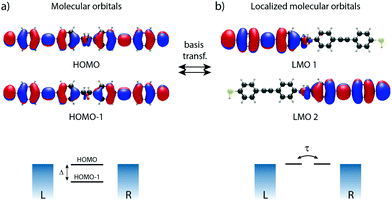
To illustrate this procedure, Fig. 7a displays the HOMO and HOMO−1 of molecule 2. As this molecule behaves according to the two-site model, only two MOs are relevant. Using the parameters of α, τ and ε1,2 obtained from Fig. 6, one can calculate the eigenvectors to be  and
and  . For this case, the LMOs can simply be obtained by addition and subtraction of the HOMO and HOMO−1, corrected with a factor of
  . The resulting LMOs are presented in Fig. 7b, each of them localized on one side of the molecule and electronically coupled to each other by an inter-site coupling equal to τ = 32 meV.
7 Measurements on the symmetric two-site molecule 1 and 2
For the experimental verification of NDC in molecule 1 and 2, the molecules were synthesized40,97 and electrically characterized using the mechanically-controllable break junction (MCBJ) technique.98 In the MCBJ technique, a gold constriction is mounted on a flexible substrate that is placed in a three-point bending mechanism. By bending the substrate, the gold wire is gradually stretched until it eventually breaks, thereby forming two atomically sharp electrodes that are suited for contacting single molecules. Here, we use lithographically-defined MCBJ samples that offer picometer control over the electrode separation.99 This breaking process can be reversed and repeated; the junction is fused by relaxing the bending of the substrate, after which the junction can be broken again. We note that the fusion “resets” the junction, so each breaking process can be distinctively different from the previous one.During the measurements presented here, the initial state of the junction is with the two gold electrodes fused. The sample is then slowly bent, which results in the two electrodes being pulled apart. Throughout this entire process, starting from the metal contact, current–voltage characteristics are continuously acquired until the noise floor of the instruments is reached. These two-terminal (2T) measurements are ideally suited to investigate the influence the electrode separation has on the junction properties. An extension for these 2T MCBJ measurements is the additional of a gate electrode.25,38,100 This third terminal only couples electrostatically to the molecule and is used to change the electrostatic potential of the molecule, i.e. the gate changes the alignment of the molecular orbitals with respect to the chemical potential of the electrodes.3,31 During such three-terminal (3T) measurements, current–voltage characteristics are recorded as a function of gate voltage.
For molecule 2, 3T measurements were employed to study the nature of the charge carriers, while for molecule 1, 2T measurements were used to investigate the influence of the electrode separation. Samples were exposed to a 0.1 mM solution of the molecule under study in dichloromethane using drop casting at room temperature. Current–voltage characteristics (IV) were recorded in a cryogenic vacuum (6.0 K, 1 × 10⁻⁶ mbar).
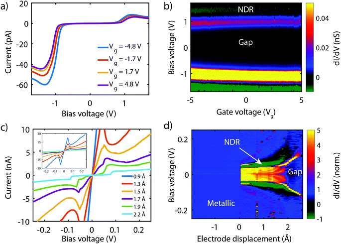
Fig. 8a presents measurements obtained on a 3T device exposed to molecule 2, obtained at different gate voltages. The first observation is that all IVs have a gap at low bias, and an onset in current at around ±1 V. Beyond this onset, the current increases and exhibits a peak around ±1.2 V. This peak is followed by a decrease in current for increasing voltage, i.e., NDC is observed. The fact that NDC occurs for both polarities points towards the symmetric version of the two-site model, with the two sites being at similar energy. Moreover, the presence of a current blockade in the IV at zero bias indicates that the Fermi energy is not on resonance with the HOMO at zero bias.40 The asymmetry in peak height is likely caused by an asymmetry in the electronic couplings, ΓL ≠ ΓR, as an asymmetric capacitive coupling would result in asymmetric peak positions.
When sweeping the voltage applied on the gate from negative to positive values, the current blockade in the IVs becomes larger; both the peak current and its position shift towards higher voltages. This behavior is more clearly visible in Fig. 8b, in which a color-coded dI/dV map as a function of both bias and gate voltage is shown. It is important to note that the gate-induced shift of the level – larger gap (larger misalignment) for more positive gate voltage – is consistent with HOMO-mediated charge transport, as expected for this molecule. Besides the shift of the gap, peak, and NDC with gate, also the peak current exhibits a gate-induced modulation. The closer the level is to the Fermi energy, the higher the peak current, which is consistent with the calculations performed in the previous section.
We now turn to molecule 1, for which Fig. 8c presents the IVs obtained on the 2T sample for increasing electrode separation. The IVs initially exhibit a clear NDC behavior. For increasing distance, the NDC peak steadily decreases and moves towards higher bias voltages, while at the same time a gap appears in the IV. This behavior is more clearly observed in the differential conductance (dI/dV), plotted as a color-coded map, as shown in Fig. 8d. The figure presents the normalized dI/dV, from the metallic regime up to the point of rupture of the molecular junction. The plot clearly illustrates the transition from NDC to a gapped IV. This transition is attributed to a change in level alignment with electrode separation, most likely due to the image-charge effect.25,93,94 Image charges are formed during charge transport through the molecule under influence of the metallic contacts, and the polarization energy associated with these charges shifts both the occupied and unoccupied levels closer to the Fermi energy. With increasing electrode separation, image-charges become weaker, and the level closest to the Fermi energy of the electrodes moves away from it. This is independent of the nature of the charge carriers (electrons, holes), and results in the formation of a gapped IV.
We note that for the two molecules the level alignment is significantly different. While for molecule 1 the HOMO is close to resonance with the Fermi energy of the electrodes, for molecule 2, it is about 0.5 eV away. Nevertheless, both molecules 1 and 2 experimentally exhibit NDC, in accordance with the chemical design principle and the DFT calculations discussed above. Moreover, for both molecules transport is dominated by the HOMO.
8 DFT calculations on the asymmetric two-site DPE-2F molecule
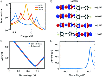
With the applicability of the two-site model verified experimentally in molecule 1 and 2, we now proceed with the realization of a single-molecule diode with molecule 3. As discussed in Section 3, introducing an asymmetry in the energies of the sites results in rectification. Molecule 3 was designed according to this principle, with the asymmetry introduced by the addition of two fluorine atoms on one side of the molecule.Fig. 9 shows a similar theoretical analysis as for the molecule 2 in Fig. 6. In contrast to the symmetric case, the transmission plot in Fig. 9a now shows a transmission peak reaching unity when a bias of 0.55 V is applied (orange curve) instead of 0.00 V; a strong suppression of transport through the HOMO and HOMO−1 occurs at 0.00 V and −0.55 V. Indeed, Fig. 9b confirms that the sites align at 0.55 V where a minimum in energy splitting between the MOs is reached. Moreover, the decreasing height of the transmission peaks when the sites are not aligned can be understood from the shape of the HOMO. Fig. 9c shows that the HOMO is strongly delocalized across the entire molecule at 0.55 V, and highly localized on one side of the molecule otherwise. Although not shown, a similar trend is observed for the HOMO−1. The calculated IV-characteristic (see Fig. 9d) is highly asymmetric and exhibits a maximum in current at the operating voltage Vp. At this bias voltage, a RR of 751 is reached.
9 Measurements on asymmetric two-site DPE-2F molecule
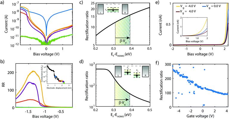
Current–voltage characteristics of molecule 3 were recorded on 2T and 3T MCBJ samples using similar experimental conditions as for molecule 1 and 2. In the 2T measurement, the junction was initially fused and gradually opened. For each step in displacement an IV was recorded, with the corresponding low-bias conductance as a function of displacement displayed in the inset of Fig. 10b. For the distances highlighted with a colored dot, the corresponding IV is presented in Fig. 10a. The distance is set to zero at the first point in conductance below 1 G0. G0 represents the quantum of conductance 2e2/h, where e is the electron charge and h Planck's constant. For distances up to 1.2 nm the IVs are symmetric, of which the blue curve is an example. Around 1.3–1.5 nm, two drops in conductance are observed, followed by a 0.75 nm long plateau. Along this plateau, IVs are highly asymmetric, with a peak in the current for negative bias voltages. The RR (see Fig. 10b) along the plateau varies between 40 and 200 and reaches a maximum in the yellow curve at a bias voltage of −1.3 V. Upon the increase of the electrode separation, the maximum current is suppressed, as is the RR. Moreover, the operating voltage shifts towards more negative voltage. Shifts in operating voltage and RR upon changing the electrode spacing as mentioned in the previous section, may be attributed to image-charge effects25,93,94 in combination with variations in the electronic coupling.59 Nevertheless, rectifying behavior is preserved up to full extension of the molecule, after which the molecular junction eventually breaks (green curve). The current then drops to just above the noise floor level of our measurement electronics and becomes symmetric again.As mentioned in the introduction, several mechanisms other than related to a two-site structure can cause rectification, and the question is therefore how these can be distinguished. It turns out that gating allows for this. In the case of a single level located between the electrodes, calculations show that the RR increases when moving the HOMO away from the Fermi energy of the electrodes (see Fig. 10c). In the two-site model, however, the RR is maximum when the HOMO is on resonance with the Fermi energy (see Fig. 10d) and decreases when the two are shifted away from each other. Thus, for both scenarios, the trend in RR is opposite and the distinction between the two can be made.
To shed light on the mechanism at play in molecule 3, we recorded IVs in gate-tunable (3T) MCBJ samples for various gate voltages. Fig. 10e shows a selection of these IVs. The IVs are highly asymmetric, with the onset of current shifting towards higher bias voltage for increasing gate voltages. Fig. 10f presents the RR as a function of the applied gate bias and shows an overall decrease in RR for increasingly positive gate voltages. Importantly, we observe a decrease in RR when moving the HOMO away from the Fermi energy (more positive gate voltage), supporting the fact that the molecule behaves according to the two-site model, rather than as a single site with an asymmetric coupling.
10 Beyond the two-site model
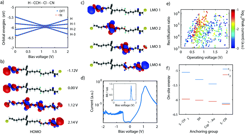
As shown in Section 4, the RR depends dramatically on the number of sites in the system. With the symmetric and asymmetric two-site model being verified both theoretically as well as experimentally, we now proceed to the theoretical investigation of molecule 4, which possesses four sites in series. Following the guidelines described in Section 5, molecule 4 was proposed,101 with ethylene groups containing only two carbon atoms used as sites. The molecule also has linkers consisting of 4 C-sp3 for an optimized inter-site coupling.Similar to the two-site case, the on-site energy can be manipulated using electronegative substituents.101 With the proper choice of side groups, the sites can be aligned at a particular bias voltage. This scenario is displayed in Fig. 11a for the H–CCH–Cl–CN substituted molecule 4. The plot shows that, as a result of the four sites being aligned at a bias voltage of 1.12 V, the four HOMOs converge and reach a minimum in energy splitting between each of them. The figure also shows that the orbital energies can be well fitted to the expression of the four-site model (fit parameters are provided in the figure caption), yielding four aligned sites.
This optimal alignment is also reflected in the MOs and LMOs. Fig. 11b shows the HOMO in various electric field conditions. For all voltages, the electrons are localized on the leftmost or rightmost site, but only at 1.12 V a fully delocalized orbital extends from one anchoring group to the other. This is a strong indication that only at that particular bias voltage electrons can efficiently be transported through the molecules. The same observation is also made for the HOMO−3, HOMO−2, and HOMO−1.
In addition, the four LMOs were computed using eqn (11), based on the wave functions of the HOMO−3 till HOMO, and the fitted four-site model parameters obtained in Fig. 11a. These LMOs are shown in Fig. 11c and are each localized on one of the sites. This observation strongly supports the description of the molecule using four weakly-coupled sites in series.
To determine the charge transport efficiency of the H–CCH–Cl–CN substituted molecule 4, we calculated its IV-characteristic using DFT + NEGF, shown in Fig. 11d on a logarithmic scale. The IV is highly asymmetric and shows a current peak at a voltage of 1.1 V. The high asymmetry becomes even more clear from the rectification ratio, shown in the inset, reaching over 1 × 10⁶. To the best of our knowledge, this rectification ratio is the highest predicted in literature for a single-molecule junction,101 exceeding even that of state-of-the-art self-assembled monolayers.79 Importantly, our mechanism is internal to the molecule, and does not rely on Coulomb interaction with the electrodes.79
To illustrate the importance of the internal level alignment of the sites, Fig. 11e presents an overview of the rectification ratios plotted versus operating biases for all combinations of side groups. The color of the data points is scaled to the logarithm of the peak current. The plot shows that depending on the combination of side groups, a large spread in rectification ratio, operating bias, and peak current is observed. The combinations with the highest peak current are located between 0.5 and 1.0 V. The corresponding rectification ratios vary between 104 and 106, with the highest ratios occurring for the largest operating voltages. This large variation in device performance illustrates the critical role of the alignment of the molecular sites. It also shows that by chemical design, one can optimize these single-molecule diodes depending on the requirements of a particular application.
The last aspect we would like to comment on is the role of the anchoring groups. Fig. 11f presents the on-site energy of a H–H–H–H substituted molecule for various anchoring groups (S-CH3, SH, Csp3–Au, and S-CN). The plot shows a large influence of the anchoring group, particularly on the energy of the outer site (ε1). Depending on the electronegativity of the anchoring group, ε1 can be shifted from −5.1 eV (S-CH3), down to −6.1 eV for (S-CN). This shows that the optimal substitution of the outer sites should explicitly take the nature of the anchoring groups into account.
11 Conclusions and outlook
In this perspective, we have illustrated the importance of orbital engineering for achieving molecular device functionality. Using two-and three-terminal MCBJ measurements, we have demonstrated that by chemical design pronounced negative differential conductance can be achieved, as well as diodes exhibiting high rectification ratios. Specifically, we predict using DFT + NEGF calculations that by introducing additional molecular sites, rectification ratios exceeding 1 million are to be expected. With the highest single-molecule rectification ratio to date being 4000,39 experimental verification of these predicted ratios would represent a drastic step forward in the field of molecular devices, with an increase in rectification ratio of several orders of magnitude, and on par with their semiconducting counterparts. Finally, the design principles presented here may be extended to generate other functionalities. For instance, as the electronic characteristics of multi-site molecules crucially depend on the internal energy alignment of the sites, one could envision the addition of side groups reacting to external stimuli to specific sites, enabling the realization of ultra-sensitive single-molecule sensors.Conflicts of interest
There are no conflicts to declare.Acknowledgements
M. P. acknowledges funding by the EMPAPOSTDOCS-II program which is financed by the European Unions Horizon 2020 research and innovation program under the Marie Skłodowska-Curie grant agreement number 754364. The work at Delft has in part been supported by the Dutch funding agency NWO.Notes and references
- A. Aviram and M. A. Ratner, Chem. Phys. Lett., 1974, 29, 277–283 CrossRef CAS.
- N. J. Tao, Nat. Nanotechnol., 2006, 1, 173–181 CrossRef CAS PubMed.
- K. Moth-Poulsen and T. Bjornholm, Nat. Nanotechnol., 2009, 4, 551 CrossRef CAS PubMed.
- S. V. Aradhya and L. Venkataraman, Nat. Nanotechnol., 2013, 8, 399–410 CrossRef CAS PubMed.
- Handbook of single-molecule electronics, ed. K. Moth-Poulsen, Jenny Stanford Publishing, 2015 Search PubMed.
- T. A. Su, M. Neupane, M. L. Steigerwald, L. Venkataraman and C. Nuckolls, Nat. Rev. Mater., 2016, 1, 2058–8437 Search PubMed.
- M. Kiguchi, Single-molecule electronics: an introduction to synthesis, measurement and theory, Springer, 2016 Search PubMed.
- J. C. Cuevas and E. Scheer, Molecular electronics: an introduction to theory and experiment, World Scientific, 2nd edn, 2017 Search PubMed.
- P. Gehring, J. M. Thijssen and H. S. van der Zant, Nat. Rev. Phys., 2019, 1, 381–396 CrossRef.
- N. Xin, J. Guan, C. Zhou, X. Chen, C. Gu, Y. Li, M. A. Ratner, A. Nitzan, J. F. Stoddart and X. Guo, Nat. Rev. Phys., 2019, 1, 211–230 CrossRef.
- F. Evers, R. Korytár, S. Tewari and J. M. Van Ruitenbeek, 2019, arXiv 1906.10449v1.
- S. J. van der Molen and P. Liljeroth, J. Phys.: Condens. Matter, 2010, 22, 133001 CrossRef PubMed.
- J. L. Zhang, J. Q. Zhong, J. D. Lin, W. P. Hu, K. Wu, G. Q. Xu, A. T. Wee and W. Chen, Chem. Soc. Rev., 2015, 44, 2998–3022 RSC.
- P. Reddy, S.-Y. Jang, R. A. Segalman and A. Majumdar, Science, 2007, 315, 1568–1571 CrossRef CAS PubMed.
- J. R. Widawsky, P. Darancet, J. B. Neaton and L. Venkataraman, Nano Lett., 2012, 12, 354–358 CrossRef CAS PubMed.
- T. Miyamachi, M. Gruber, V. Davesne, M. Bowen, S. Boukari, L. Joly, F. Scheurer, G. Rogez, T. K. Yamada, P. Ohresser, E. Beaurepaire and W. Wulfhekel, Nat. Commun., 2012, 3, 938 CrossRef PubMed.
- R. Frisenda, G. D. Harzmann, J. A. Celis Gil, J. M. Thijssen, M. Mayor and H. S. J. van der Zant, Nano Lett., 2016, 16, 4733–4737 CrossRef CAS PubMed.
- J. Park, A. N. Pasupathy, J. I. Goldsmith, C. Chang, Y. Yaish, J. R. Petta, M. Rinkoski, J. P. Sethna, H. D. Abruna, P. L. McEuen and D. C. Ralph, Nature, 2002, 417, 722–725 CrossRef CAS PubMed.
- W. J. Liang, M. P. Shores, M. Bockrath, J. R. Long and H. Park, Nature, 2002, 417, 725–729 CrossRef CAS PubMed.
- J. J. Parks, A. R. Champagne, T. A. Costi, W. W. Shum, A. N. Pasupathy, E. Neuscamman, S. Flores-Torres, P. S. Cornaglia, A. A. Aligia, C. A. Balseiro, G. K.-L. Chan, H. D. Abruña and D. C. Ralph, Science, 2010, 328, 1370–1373 CrossRef CAS PubMed.
- H. B. Heersche, Z. de Groot, J. A. Folk, H. S. J. van der Zant, C. Romeike, M. R. Wegewijs, L. Zobbi, D. Barreca, E. Tondello and A. Cornia, Phys. Rev. Lett., 2006, 96, 206801 CrossRef CAS PubMed.
- A. R. Champagne, A. N. Pasupathy and D. C. Ralph, Nano Lett., 2005, 5, 305–308 CrossRef CAS PubMed.
- S. Y. Quek, M. Kamenetska, M. L. Steigerwald, H. J. Choi, S. G. Louie, M. S. Hybertsen, J. B. Neaton and L. Venkataraman, Nat. Nanotechnol., 2009, 4, 230–234 CrossRef CAS PubMed.
- C. Bruot, J. Hihath and N. Tao, Nat. Nanotechnol., 2012, 7, 35–40 CrossRef CAS PubMed.
- M. Perrin, C. Verzijl, C. Martin, A. Shaikh, R. Eelkema, J. Van Esch, J. Van Ruitenbeek, J. Thijssen, H. Van Der Zant and D. Dulić, Nat. Nanotechnol., 2013, 8, 282–287 CrossRef CAS PubMed.
- D. Stefani, K. Weiland, M. Skripnik, C. Hsu, M. Perrin, M. Mayor, F. Pauly and H. Van Der Zant, Nano Lett., 2018, 18, 5981–5988 CrossRef CAS.
- L. Venkataraman, J. E. Klare, C. Nuckolls, M. S. Hybertsen and M. L. Steigerwald, Nature, 2006, 442, 904–907 CrossRef CAS PubMed.
- C. Li, I. Pobelov, T. Wandlowski, A. Bagrets, A. Arnold and F. Evers, J. Am. Chem. Soc., 2008, 130, 318–326 CrossRef CAS PubMed.
- H. Park, A. K. L. Lim, A. P. Alivisatos, J. Park and P. L. McEuen, Appl. Phys. Lett., 1999, 75, 301–303 CrossRef CAS.
- S. Kubatkin, A. Danilov, M. Hjort, J. Cornil, J. L. Bredas, N. Stuhr-Hansen, P. Hedegard and T. Bjornholm, Nature, 2003, 425, 698–701 CrossRef CAS PubMed.
- M. L. Perrin, E. Burzurí and H. S. J. van der Zant, Chem. Soc. Rev., 2015, 44, 902–919 RSC.
- M. Elbing, R. Ochs, M. Koentopp, M. Fischer, C. von Hanisch, F. Weigend, F. Evers, H. B. Weber and M. Mayor, Proc. Natl. Acad. Sci. U. S. A., 2005, 102, 8815–8820 CrossRef CAS PubMed.
- I. Diez-Perez, J. Hihath, Y. Lee, L. Yu, L. Adamska, M. A. Kozhushner, I. I. Oleynik and N. Tao, Nat. Chem., 2009, 1, 635–641 CrossRef CAS PubMed.
- E. Lörtscher, B. Gotsmann, Y. Lee, L. Yu, C. Rettner and H. Riel, ACS Nano, 2012, 6, 4931–4939 CrossRef.
- B. Capozzi, J. Xia, O. Adak, E. J. Dell, Z.-F. Liu, J. C. Taylor, J. B. Neaton, L. M. Campos and L. Venkataraman, Nat. Nanotechnol., 2015, 10, 522–527 CrossRef CAS.
- S. Sherif, G. Rubio-Bollinger, E. Pinilla-Cienfuegos, E. Coronado, J. C. Cuevas and N. Agraït, Nanotechnology, 2015, 26, 291001 CrossRef PubMed.
- C. Guo, K. Wang, E. Zerah-Harush, J. Hamill, B. Wang, Y. Dubi and B. Xu, Nat. Chem., 2016, 8, 484–490 CrossRef CAS.
- M. Perrin, E. Galán, R. Eelkema, J. Thijssen, F. Grozema and H. Van Der Zant, Nanoscale, 2016, 8, 8919–8923 RSC.
- A. C. Aragonès, N. Darwish, S. Ciampi, F. Sanz, J. J. Gooding and I. Díez-Pérez, Nat. Commun., 2017, 8, 15056 CrossRef PubMed.
- M. L. Perrin, R. Frisenda, M. Koole, J. S. Seldenthuis, J. A. Gil, H. Valkenier, J. C. Hummelen, N. Renaud, F. C. Grozema, J. M. Thijssen, D. Dulić and H. S. Van Der Zant, Nat. Nanotechnol., 2014, 9, 830–834 CrossRef CAS PubMed.
- D. Dulić, S. J. van der Molen, T. Kudernac, H. T. Jonkman, J. J. D. de Jong, T. N. Bowden, J. van Esch, B. L. Feringa and B. J. van Wees, Phys. Rev. Lett., 2003, 91, 207402 CrossRef PubMed.
- C. Jia, A. Migliore, N. Xin, S. Huang, J. Wang, Q. Yang, S. Wang, H. Chen, D. Wang, B. Feng, Z. Liu, G. Zhang, D. H. Qu, H. Tian, M. A. Ratner, H. Q. Xu, A. Nitzan and X. Guo, Science, 2016, 352, 1443–1445 CrossRef CAS PubMed.
- X. H. Qiu, G. V. Nazin and W. Ho, Science, 2003, 299, 542–546 CrossRef CAS PubMed.
- S. Battacharyya, A. Kibel, G. Kodis, P. A. Liddell, M. Gervaldo, D. Gust and S. Lindsay, Nano Lett., 2011, 11, 2709–2714 CrossRef CAS PubMed.
- E. Loertscher, J. M. Tour, J. W. Ciszek and H. Riel, J. Phys.: Conf. Ser., 2007, 61, 987–991 CrossRef.
- L. Rincón-García, C. Evangeli, G. Rubio-Bollinger and N. Agraït, Chem. Soc. Rev., 2016, 45, 4285–4306 RSC.
- J. S. Meisner, M. Kamenetska, M. Krikorian, M. L. Steigerwald, L. Venkataraman and C. Nuckolls, Nano Lett., 2011, 11, 1575–1579 CrossRef CAS PubMed.
- Y. S. Park, A. C. Whalley, M. Kamenetska, M. L. Steigerwald, M. S. Hybertsen, C. Nuckolls and L. Venkataraman, J. Am. Chem. Soc., 2007, 129, 15768–15769 CrossRef CAS PubMed.
- W. Hong, D. Z. Manrique, P. Moreno-García, M. Gulcur, A. Mishchenko, C. J. Lambert, M. R. Bryce and T. Wandlowski, J. Am. Chem. Soc., 2012, 134, 2292–2304 CrossRef CAS.
- E. Leary, A. La Rosa, M. T. Gonz'alez, G. Rubio-Bollinger, N. Agraït and N. Martín, Chem. Soc. Rev., 2014, 44, 920–942 RSC.
- R. Frisenda, S. Tarkuç, E. Galán, M. Perrin, R. Eelkema, F. Grozema and H. van der Zant, Beilstein J. Nanotechnol., 2015, 6, 1558–1567 CrossRef CAS.
- A. Vladyka, M. Perrin, J. Overbeck, R. Ferradás, V. García-Suárez, M. Gantenbein, J. Brunner, M. Mayor, J. Ferrer and M. Calame, Nat. Commun., 2019, 10, 262 CrossRef PubMed.
- L. Venkataraman, Y. S. Park, A. C. Whalley, C. Nuckolls, M. S. Hybertsen and M. L. Steigerwald, Nano Lett., 2007, 7, 502–506 CrossRef CAS PubMed.
- X. Y. Xiao, L. A. Nagahara, A. M. Rawlett and N. J. Tao, J. Am. Chem. Soc., 2005, 127, 9235–9240 CrossRef CAS PubMed.
- A. Mishchenko, D. Vonlanthen, V. Meded, B. Marius, C. Li, I. V. Pobelov, A. Bagrets, J. K. Viljas, F. Pauly, F. Evers, M. Mayor and T. Wandlowski, Nano Lett., 2010, 10, 156–163 CrossRef CAS PubMed.
- Y. Li, M. Buerkle, G. Li, A. Rostamian, H. Wang, Z. Wang, D. R. Bowler, T. Miyazaki, L. Xiang, Y. Asai, G. Zhou and N. Tao, Nat. Mater., 2019, 18, 357–363 CrossRef CAS PubMed.
- J. Bai, A. Daaoub, S. Sangtarash, X. Li, Y. Tang, Q. Zou, H. Sadeghi, S. Liu, X. Huang, Z. Tan, J. Liu, Y. Yang, J. Shi, G. Mészáros, W. Chen, C. Lambert and W. Hong, Nat. Mater., 2019, 18, 364–369 CrossRef CAS PubMed.
- C. M. Guédon, H. Valkenier, T. Markussen, K. S. Thygesen, J. C. Hummelen and S. J. Van Der Molen, Nat. Nanotechnol., 2012, 7, 305–309 CrossRef PubMed.
- R. Frisenda and H. S. J. van der Zant, Phys. Rev. Lett., 2016, 117, 126804 CrossRef CAS PubMed.
- M. Paulsson, F. Zahid and S. Datta, Handbook of Nanoscience, Engineering, and Technology, 3rd edn, CRC Press, 2012 Search PubMed.
- P. E. Kornilovitch, A. M. Bratkovsky and R. Stanley Williams, Phys. Rev. B: Condens. Matter Mater. Phys., 2002, 66, 165436 CrossRef.
- A. Batra, J. S. Meisner, P. Darancet, Q. Chen, C. Steigerwald, M. L. Nuckolls and L. Venkataraman, Faraday Discuss., 2014, 174, 79–89 CAS.
- T. Kim, Z. F. Liu, C. Lee, J. B. Neaton and L. Venkataraman, Proc. Natl. Acad. Sci. U. S. A., 2014, 111, 10928–10932 CrossRef CAS PubMed.
- G. M. Morales, P. Jiang, S. Yuan, Y. Lee, A. Sanchez, W. You and L. Yu, J. Am. Chem. Soc., 2005, 10456–10457 CrossRef CAS PubMed.
- J. Hihath, C. Bruot, H. Nakamura, Y. Asai, I. Diez-Perez, Y. Lee, L. Yu and N. Tao, ACS Nano, 2011, 5, 8331–8339 CrossRef CAS PubMed.
- W. Wang and L. Yu, Langmuir, 2011, 27, 2084–2087 CrossRef CAS PubMed.
- A. Batra, P. Darancet, Q. Chen, J. S. Meisner, J. R. Widawsky, J. B. Neaton, C. Nuckolls and L. Venkataraman, Nano Lett., 2013, 13, 6233–6237 CrossRef CAS.
- K. Wang, J. Zhou, J. M. Hamill and B. Xu, J. Chem. Phys., 2014, 141, 054712 CrossRef.
- V. C. Zoldan, R. Faccio and A. A. Pasa, Sci. Rep., 2015, 5, 8350 CrossRef PubMed.
- S. Fujii, T. Tada, Y. Komoto, T. Osuga, T. Murase, M. Fujita and M. Kiguchi, J. Am. Chem. Soc., 2015, 137, 5939–5947 CrossRef CAS PubMed.
- J. E. Meany, M. S. Johnson, S. A. Woski and R. M. Metzger, ChemPlusChem, 2016, 81, 1152–1155 CrossRef CAS.
- M. Koepf, C. Koenigsmann, W. Ding, A. Batra, C. F. Negre, L. Venkataraman, G. W. Brudvig, V. S. Batista, C. A. Schmuttenmaer and R. H. Crabtree, Nanoscale, 2016, 8, 16357–16362 RSC.
- R. Yamada, K. Albrecht, T. Ohto, K. Minode, K. Yamamoto and H. Tada, Nanoscale, 2018, 10, 19818–19824 RSC.
- S. Fujii, F. Ishiwari, Y. Komoto, L. Su, Y. Yamagata, A. Kosaka, A. Aiba, T. Nishino, T. Fukushima and M. Kiguchi, Jpn. J. Appl. Phys., 2019, 58, 035003 CrossRef CAS.
- M. Handayani, H. Tanaka, S. Katayose, T. Ohto, Z. Chen, R. Yamada, H. Tada and T. Ogawa, Nanoscale, 2019, 11, 22724–22729 RSC.
- G. J. Ashwell, W. D. Tyrrell and A. J. Whittam, J. Am. Chem. Soc., 2004, 126, 7102–7110 CrossRef CAS PubMed.
- S. Casalini, C. A. Bortolotti, F. Leonardi and F. Biscarini, Chem. Soc. Rev., 2017, 46, 40–71 RSC.
- L. Yuan, R. Breuer, L. Jiang, M. Schmittel and C. A. Nijhuis, Nano Lett., 2015, 15, 9556–9563 Search PubMed.
- X. Chen, M. Roemer, L. Yuan, W. Du, D. Thompson, E. del Barco and C. A. Nijhuis, Nat. Nanotechnol., 2017, 12, 797–803 CrossRef CAS PubMed.
- H. Mizuta and T. Tanoue, The Physics and Applications of Resonant Tunnelling Diodes, Cambridge University Press, 2006 Search PubMed.
- B. R. Charlie Ironside and J. Figueiredo, Resonant Tunneling Diode Photonics, Morgan & Claypool Publishers, 2019 Search PubMed.
- Rectifier Circuits, ed. W. F. Waller, Macmillan Education, UK, 1972 Search PubMed.
- C.-T. Sah, Fundamentals of solid-state electronics, World Scientific, 1991, p. 1010 Search PubMed.
- A.-P. Jauho, N. S. Wingreen and Y. Meir, Phys. Rev. B: Condens. Matter Mater. Phys., 1994, 50, 5528–5544 CrossRef CAS PubMed.
- H. Haug and A.-P. Jauho, Quantum Kinetics in Transport and Optics of Semiconductors, Springer, Berlin, Heidelberg, 1997 Search PubMed.
- Y. Meir and N. S. Wingreen, Phys. Rev. Lett., 1992, 68, 2512–2515 CrossRef PubMed.
- G. te Velde and E. J. Baerends, Phys. Rev. B: Condens. Matter Mater. Phys., 1991, 44, 7888–7903 CrossRef CAS.
- C. Fonseca Guerra, J. G. Snijders, G. te Velde and E. J. Baerends, Theor. Chem. Acc., 1998, 99, 391–403 Search PubMed.
- C. J. Verzijl, J. S. Seldenthuis and J. M. Thijssen, J. Chem. Phys., 2013, 138, 094102 CrossRef CAS PubMed.
- F. Mirjani, J. M. Thijssen and S. J. Van Der Molen, Phys. Rev. B: Condens. Matter Mater. Phys., 2011, 84, 115402 CrossRef.
- S. K. S. Mazinani, R. V. Meidanshahi, J. L. Palma, P. Tarakeshwar, T. Hansen, M. A. Ratner and V. Mujica, J. Phys. Chem. C, 2016, 26054–26060 CrossRef CAS.
- C. Van Dyck and A. J. Bergren, Adv. Electron. Mater., 2018, 4, 1700656 CrossRef.
- K. Kaasbjerg and K. Flensberg, Nano Lett., 2008, 8, 3809–3814 CrossRef CAS PubMed.
- C. Verzijl, J. Celis Gil, M. Perrin, D. Dulić, H. Van Der Zant and J. Thijssen, J. Chem. Phys., 2015, 143, 174106 CrossRef CAS PubMed.
- M. Kilgour and D. Segal, J. Chem. Phys., 2015, 143, 024111 CrossRef PubMed.
- H. Valkenier, C. M. Guedon, T. Markussen, K. S. Thygesen, S. J. van der Molen and J. C. Hummelen, Phys. Chem. Chem. Phys., 2013, 16, 653–662 RSC.
- E. Galán, M. Perrin, M. Lutz, H. Van Der Zant, F. Grozema and R. Eelkema, Org. Biomol. Chem., 2016, 14, 2439–2443 RSC.
- J. M. van Ruitenbeek, A. Alvarez, I. Piñeyro, C. Grahmann, P. Joyez, M. H. Devoret, D. Esteve and C. Urbina, Rev. Sci. Instrum., 1996, 67, 108–111 CrossRef CAS.
- C. A. Martin, R. H. Smit, R. V. Egmond, H. S. Van Der Zant and J. M. Van Ruitenbeek, Rev. Sci. Instrum., 2011, 82, 053907 CrossRef PubMed.
- C. A. Martin, J. M. van Ruitenbeek and H. S. J. van der Zant, Nanotechnology, 2010, 21, 265201 CrossRef PubMed.
- M. Perrin, M. Doelman, R. Eelkema and H. Van Der Zant, Phys. Chem. Chem. Phys., 2017, 19, 29187–29194 RSC.
| This journal is © the Owner Societies 2020 |


