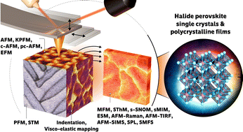
Scanning probe microscopy (SPM) and advanced atomic force microscopy (AFM++) have become pivotal for nanoscale elucidation of the structural, optoelectronic and photovoltaic properties of halide perovskite single crystals and polycrystalline films, both under ex situ and in situ conditions. These techniques reveal detailed information about film topography, compositional mapping, charge distribution, near-field electrical behaviors, cation–lattice interactions, ion dynamics, piezoelectric characteristics, mechanical durability, thermal conductivity, and magnetic properties of doped perovskite lattices. This article outlines the advancements in SPM techniques that deepen our understanding of the optoelectronic and photovoltaic performances of halide perovskites.
