
 Open Access Article
 This Open Access Article is licensed under a Creative Commons Attribution-Non Commercial 3.0 Unported Licence
Highly selective ammonia sensing at room temperature using DC plasma-modified MoS2 nanoflowers†
Anurag
Kashyap
 a,
Bipradip
Chakraborty
b,
Tonmoi
Hazarika
c,
Sanjeeb
Chouhan
a,
Bharat
Kakati
c and
Hemen
Kalita
*a
a,
Bipradip
Chakraborty
b,
Tonmoi
Hazarika
c,
Sanjeeb
Chouhan
a,
Bharat
Kakati
c and
Hemen
Kalita
*a
aNanomaterials and Nanoelectronics Laboratory, Department of Physics, Gauhati University, Guwahati – 781014, Assam, India. E-mail: hemenkalita@gauhati.ac.in; Tel: +91 9769511692
bDepartment of Applied Science, Gauhati University, Guwahati – 781014, Assam, India
cMETA Laboratory, Assam Science and Technology University, Guwahati – 781013, Assam, India
First published on 28th April 2025
Abstract
This study explored the enhancement of ammonia (NH3) sensing properties of MoS2 nanoflowers through a direct current (DC) plasma treatment with nitrogen incorporation. Plasma treatment induced sulfur vacancies and introduced nitrogen atoms into the MoS2 surfaces, enhancing the number of active sites and improving the charge carrier mobility. The structural and chemical alterations were confirmed by characterisations using FE-SEM, XPS, and Raman spectroscopy. The resulting plasma-treated MoS2 sensor demonstrated highly selective detection of NH3 at room temperature with a rapid response time of 22 s and a recovery time of 23 s. The experimental limit of detection was achieved at 5 ppm (theoretically ≈ 80 ppb), which was lower than the safety threshold set by the National Institute for Occupational Safety and Health (NIOSH). Results of DFT studies also agreed with the experimental results. Thus, this work highlights DC plasma treatment as an efficient, cost-effective approach to enhance gas sensing performance, with implications for developing highly sensitive and selective sensors for environmental monitoring and safety applications.
1. Introduction
In recent years, the detection of toxic gases has gained increasing importance in various fields, ranging from air quality control and workplace safety to medical diagnostics.1–3 In particular, detection of ammonia (NH3) has received significant interest owing to its adverse health effects, including severe respiratory conditions like asthma, emphysema, and chronic bronchitis, even when exposed to low levels.4 Different types of sensing technologies, such as electrochemical cells and metal oxide chemiresistors, have been reported for the commercial detection of toxic gases.5 However, these sensors often face challenges, such as the need for high operating temperatures and poor selectivity for differentiating between various gases.To address these limitations, researchers have focused on alternative materials, particularly low-dimensional materials. Owing to their unique physiochemical properties, such as large specific surface areas, distinct electrical properties, and ease of functionalisation, 2D materials have gained significant importance in gas sensing in recent years.4,6,7 Among the 2D materials, transition metal dichalcogenides (TMDs) are promising candidates for fabricating highly sensitive gas and volatile organic compound (VOC) sensors.8 These materials provide weak gas-molecule binding and efficient charge transfer, enabling gas detection at room temperature.9,10 Among the TMDs, molybdenum disulfide (MoS2) has sparked a lot of research interest as a prominent sensing material owing to its high surface-to-volume ratio, high surface activity and sensitivity, quick response time, and outstanding stability.11–16 In fact, MoS2 is more appealing than graphene-based gas sensors owing to its semiconducting nature and the appropriate, adjustable band gap energies.17 Despite its potential, MoS2 still suffers from selectivity issues owing to similar VOC adsorption energies, making it difficult to detect one gas without interference from the other.18,19 To overcome this, advanced fabrication techniques have been implemented, including doping, intercalation, and the creation of heterostructures, enhancing the material's ability to target specific gases more effectively.20–24
Plasma treatment is a prevalent method to alter the inherent physical and chemical properties of TMDs for application in gas sensing, ion storage, and oxygen reduction and hydrogen evolution reactions.5,25–28 RF plasma treatment is commonly employed to alter surfaces because of its ability to provide homogeneous treatments applicable to 2D, complicated, and 3D materials.29 The direct current plasma (DC plasma) treatment is another method by which material sensing properties can be modified by incorporating surface defects.30,31 The procedure involves high-energy ions and reactive plasma species that alter the surface morphology and electronic characteristics. The creation of defects such as vacancies, surface states, and dangling bonds results in such changes, which increase the surface area. These modifications increase the sensitivity of the ability to adsorb the analyte, facilitate charge transfer, and thus increase the sensitivity and selectivity of the sensor. Moreover, plasma treatment with DC offers an avenue to modify sensor surfaces because it is extremely adaptable, less expensive than RF plasma, and suitable for a variety of materials.31 Plasma processing has recently demonstrated itself as a rapid, convenient, straightforward, and effective approach for modifying the surface chemical characteristics of materials, particularly for the treatment of 2D materials without solvent contamination.32,33 The chemical properties of the plasma process gas are crucial for determining the reaction mechanisms involved in plasma surface modification. Various gases, including oxygen, argon, helium, nitrogen, ammonia, carbon dioxide, and water, are used as process gases in surface modification techniques using plasma.34 This approach may produce additional edge sites and heteroatoms, enhancing their charge carrier mobility and catalytic and optoelectronic capabilities.35,36 Among the many existing methodologies, nitrogen plasma treatment has recently been recognized as an excellent approach for achieving controlled nitrogen atom incorporation into TMDs.5,28,34,37 Zhao et al. developed an N-doped MoS2 nanosheet-based sensor with improved sensitivity to NO2 at room temperature.28 Initially, MoS2 nanosheets were hydrothermally fabricated and N-doping was performed via nitrogen plasma to synthesize N-MoS2 nanosheets. Nitrogen atoms were introduced using a plasma-assisted technique. The atoms were adsorbed on the surface and doped into the lattice defects of MoS2. This modified the electronic properties, such as the reduction of the Fermi level and the narrowing of the band gap.36 The structure increased the conductivity and sensitization with NO2, thereby increasing the response and reducing the detection limit.
This study reported the effects of DC plasma treatment on the NH3 sensitivity of the MoS2 nanoflower structure. Plasma-treated MoS2 shows selective detection of NH3 at RT (25 °C), greatly improving its sensing performance. N-MoS2 sensor has a faster response time of 22 s and takes 23 s to recover. Moreover, plasma treatment significantly stabilized the sensing response of the sensor. The experimental and theoretical limits of detection were 5 ppm and 80 ppb, respectively. An effective way of improving room temperature NH3 detection is described in this study.
2. Experimental section
2.1. Materials
Sodium molybdate (Na2MoO4·2H2O), thioacetamide (CH3CSNH2), and oxalic acid (H2C2O4) were obtained from Sisco Research Laboratories (SRL) and used as received. The plasma treatment was performed using a glow discharge plasma reactor to produce N2 and Ar plasma. Fig. 1 shows a schematic of the experimental assembly. Deionised water (DIW) was used throughout the experiment. | ||
| Fig. 1 Schematic of (a) synthesis of MoS2 nanoflowers following the wet chemical route and (b) plasma treatment assembly with digital images of Ar and N2 plasma during treatment. | ||
2.2. Synthesis of MoS2
A wet chemical route is followed to synthesize MoS2 nanoflowers. In a typical reaction, 1 g of sodium molybdate and 1.2 g of thioacetamide are stirred in 50 mL of DI water for 30 min at ambient temperature. Then, 0.6 g of oxalic acid was added to the mixture, which was further stirred for another 30 min. The solution was then hydrothermally treated for 24 h at 200 °C by being put in a 100 mL Teflon beaker and sealed inside a stainless steel (SS) container. After cooling to room temperature, the sample is centrifuged with ethanol and DI water and freeze-dried for 24 h.2.3. Sensor electrode fabrication
Interdigitated electrode structures (IDE) have been fabricated following a standard copper (Cu) etching procedure using a ferric chloride (FeCl3) solution. The desired IDE structure was transferred to the copper printed circuit board (PCB), which was dipped in FeCl3 solution following agitation for the etching of the unwanted copper. Finally, the IDE structure remains on the board and is rinsed with ethanol and DI water and dried by purging nitrogen before deposition of the sensing material.2.4. Synthesis of N-MoS2
As nitrogen plasma is treated on the sensor, the sensor is termed as N-MoS2 in the entire report. Sensors were treated with an argon/nitrogen plasma produced from a custom-built glow discharge reactor. The sensor was fabricated using the drop-casting method. The synthesized MoS2 sample was dispersed and drop-cast on sensors composed of copper IDEs and dried in a vacuum oven at 60 °C for 3 h before plasma treatment. Fig. 1(b) shows a schematic of the experimental setup. The plasma chamber, a cylindrical stainless steel (SS 304L) vessel with a volume of approximately 3.5 × 103 cm3 (diameter: 30.0 cm, height: 50.0 cm), was evacuated using a diffusion pump (1000 L min−1) backed by a rotary pump (540 L s−1). A base pressure of ∼10−6 mbar was achieved.Two circular stainless steel (SS 304L) electrodes initiated the discharge and were powered by a DC power supply (1000 V, 2.5 A). Ultra-pure argon/nitrogen gas (99.99%) was introduced into the chamber through a digital flow controller to maintain a working pressure of 1.0 × 10⁻¹ mbar. The sensors were exposed to Ar and N2 plasma for 2 and 10 minutes, respectively.
A Langmuir probe was used for plasma diagnostics. The measured plasma density was 4.35 × 10¹⁵ m−3 and 4.43 × 10¹⁵ m−3 in the presence and absence of sensors, respectively. The electron temperature remained relatively constant at 1.38 eV. The slight decrease in plasma density observed in the presence of sensors is attributed to plasma-sample interactions.34,38
2.5. Computational details
The computations conducted utilised the density functional theory (DFT) – based Cambridge Serial Total Energy Package (CASTEP) module, which is integrated into the Materials Studio software suite.4,7,39 The Kohn–Sham equations were solved using the plane-wave pseudopotential method developed within the DFT framework.40 For the exchange–correlation function, the generalized gradient approximation (GGA), as outlined by Perdew–Burke–Ernzerhof (PBE), was used for geometry optimization.41 Throughout the computations, the DFT-D dispersion correction suggested by Grimme and used in CASTEP was used to account for the van der Waals (vdW) intermolecular forces.42 A 6 × 6 × 1 k-point mesh was used to sample the Brillouin zone with an energy cutoff of 517 eV. Geometry optimization, which is essential for achieving a configuration's equilibrium state with minimum energy, was performed using the Broyden–Fletcher–Goldfarb–Shanno (BFGS) algorithm, which is highly effective for energy minimization in crystalline materials.43A medium convergence tolerance was adopted for geometry optimization, and electronic minimization parameters utilized the Gaussian smearing scheme with a smearing width of 0.1 eV. Additionally, a 20 Å vacuum was introduced perpendicular to the interface surface to eliminate interactions between the interfaces and their periodic images.
The difference in charge density between the MoS2 system and the adsorbed gas is computed as:
| Δρ = ρ(MoS2+gas_molecule) − ρgas_molecule | (1) |
The binding energy of the adsorbed gas molecules is calculated using the equation:
| Eb = E(MoS2+gas_molecule) − E(gasmolecule) | (2) |
2.6. Characterization
The morphology of the synthesized samples were observed using field emission-scanning electron microscope (FE-SEM, ΣIGMA 300 VP, Carl Zeiss). The structural characteristics of the fabricated samples were characterized using an X-ray diffractometer (XPERT PRO, Philips/PANalytical) with Cu Kα radiation (1.54 Å) and with a laser micro-Raman system (Make: Horiba JobinYvon, Model: LabRam HR). XPS analyses were performed using an X-ray Photo Spectrometer (Model-K Alpha, Make: Thermo Fisher Scientific).3. Results and discussions
3.1. Structural and morphological characterizations of MoS2 and N-MoS2
Fig. 2 shows the FESEM images and EDX analysis of MoS2 and N-MoS2. As shown in Fig. 2(a), the MoS2 nanosheets are arranged in a flower-like structure. EDX analysis (Fig. 2(c)) provides elemental information about the synthesized materials. In the case of N-MoS2 (Fig. 2(b)), the flower-like structure is intact with a bit of deformation, which may be due to the bombardment of energetic ions during argon plasma treatment, followed by nitrogen plasma. The EDX spectrum (Fig. 2(d)) shows the presence of nitrogen, which is absent in the EDX spectrum of MoS2 (Fig. 2(c)). The colour-mapping images of different elements present in the nitrogen-incorporated MoS2 sample are shown in Fig. 2(e-h).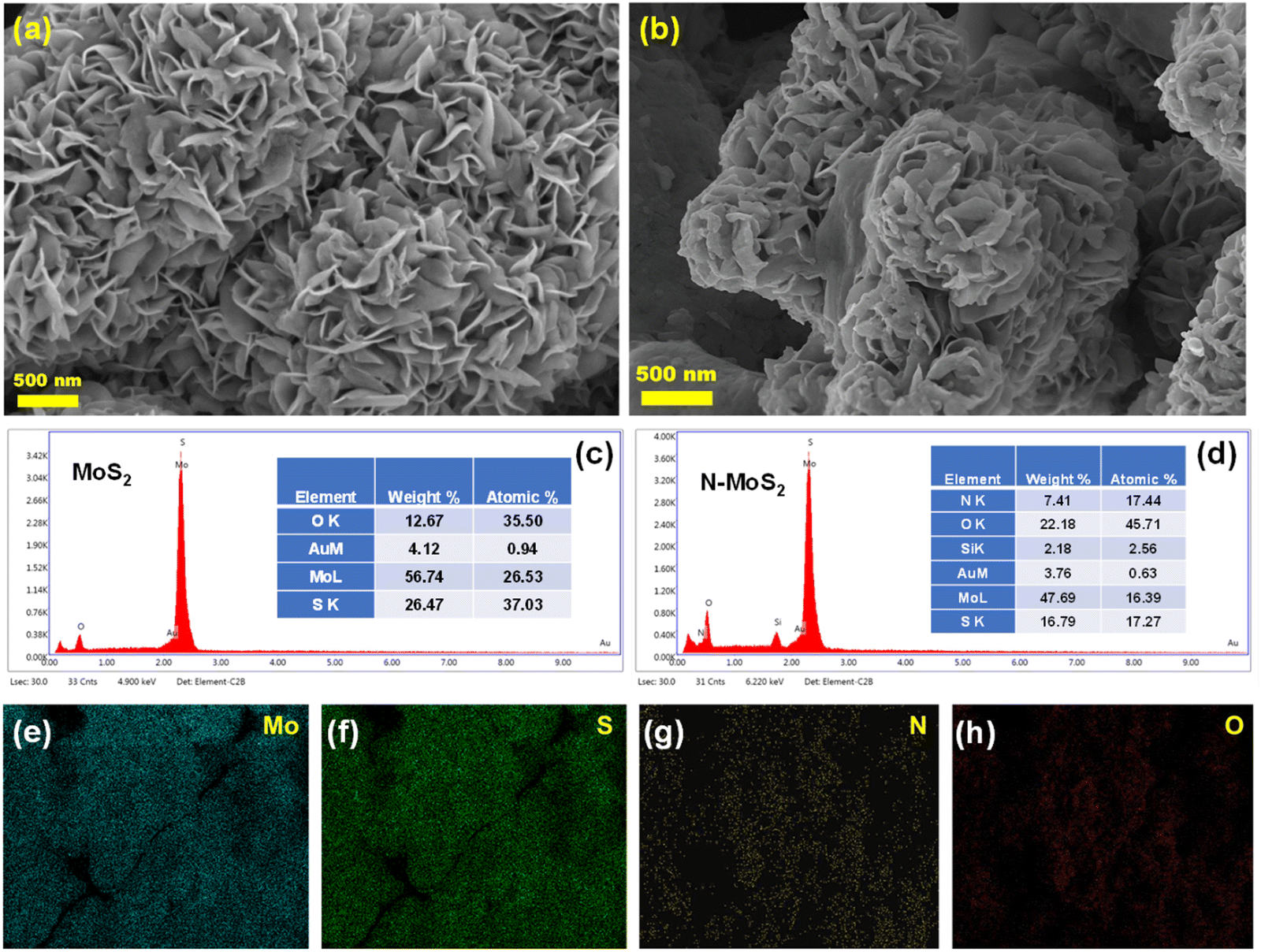 | ||
| Fig. 2 FESEM images of (a) MoS2 nanosheet and (b) N-MoS2 nanosheet; EDX spectra of (c) MoS2 and (d) N-MoS2; and (e)–(h) colour mapped images of Mo, S, N and O elements of N-MoS2 sample. | ||
Fig. 3(a) shows the Raman spectra of MoS2 and N-MoS2, in which two distinct peaks E12g and A1g represent the vibration modes of hexagonal MoS2. The A1g peak that appears at ∼ 402 cm−1 is attributed to the out-of-plane vibration of Mo and S atoms, whereas E12g appears at ∼375 cm−1 and is attributed to the in-plane vibration of Mo and S atoms.44 The peak spacing between the E12g and A1g peaks for both MoS2 and N-MoS2 was the same (26.4 cm−1), confirming their similar layer numbers.44 The Raman spectra of MoS2 after various nitrogen plasma treatment times are presented in the ESI† (Fig. S1). The X-ray diffraction patterns of the synthesized MoS2 nanoflowers and bulk MoS2 are presented in the ESI† (Fig. S2). Fig. 3(b) shows the XPS survey spectra of MoS2 and N-MoS2. From this figure, the N/Mo ratios are 0.5 and 3.3 for MoS2 and N-MoS2, respectively. Fig. 3(c)–(h) shows the deconvoluted XPS spectra of the MoS2 and N-MoS2 samples. In Fig. 3(c), the Mo 3d spectrum of MoS2 exhibits four peaks, among which Mo4+ 3d5/2 and Mo4+ 3d3/2 correspond to 228.9 eV and 232.0 eV, respectively.45 Along with this, a small peak around 235 eV appears due to the oxidation of Mo on the MoS2 surface and is assigned to Mo6+ 3d3/2 and Mo6+ 3d5/2, respectively.46 The peak at 226.1 eV was assigned to the S 2s of MoS2.45 For N-MoS2, the deconvoluted spectrum of Mo 3d in Fig. 3(f) shows the peak present at 233.5 eV along with the peaks present in Fig. 3(c), which arise due to bonds between Mo and N.28,47,48 Moreover, the intensity of the Mo6+ 3d peaks increased, which may have been due to the oxidation of Mo after treatment.
 | ||
| Fig. 3 (a) Raman spectra of MoS2 and N-MoS2 XPS; (b) XPS survey spectra of MoS2 and N-MoS2; XPS deconvoluted spectra of (c) Mo 3d, (d) S 2p, and (e) Mo 3p of the MoS2 sample and (f) Mo 3d, (g) S 2p, and (h) Mo 3p of the N-MoS2 sample. | ||
Fig. 3(d) and (g) show the S 2p spectra of MoS2 and N-MoS2, respectively. Two peaks appear at 163.1 and 161.7 eV, corresponding to S2− 2p1/2 and S2− 2p3/2, respectively.28Fig. 3(e) and (h) show the Mo 3p spectra of MoS2 and N-MoS2, respectively. The peaks at 394.7 eV arise due to Mo 3p3/2 in both spectra. Along with that, two distinct and intense peaks in Fig. 3(h) at 398.5 eV and 402.0 eV appear due to characteristic Mo–N bond and N–O, respectively, which are less intense in the case of the Mo 3p deconvoluted spectrum of MoS2 (Fig. 3(e)).47,49
3.2. Gas sensing measurements of the MoS2 and N-MoS2 sensors:
The gas sensing measurements of the MoS2 and N-MoS2 sensors were performed in a homemade sensing assembly (Fig. 4). The sensing material was dropcasted onto the interdigitated electrode fabricated on the PCB, as described in Section 2.3. The sensor was then dried in a vacuum oven at 60 °C for 3 h. The sensor was then plasma-treated with argon and nitrogen plasma in a plasma chamber. The sensor was then exposed to VOCs in the gas sensing chamber (Fig. 4). The required amount of ammonia, calculated using the standard formula (ESI,† eqn (S1)), was inserted inside the sensing chamber.4,7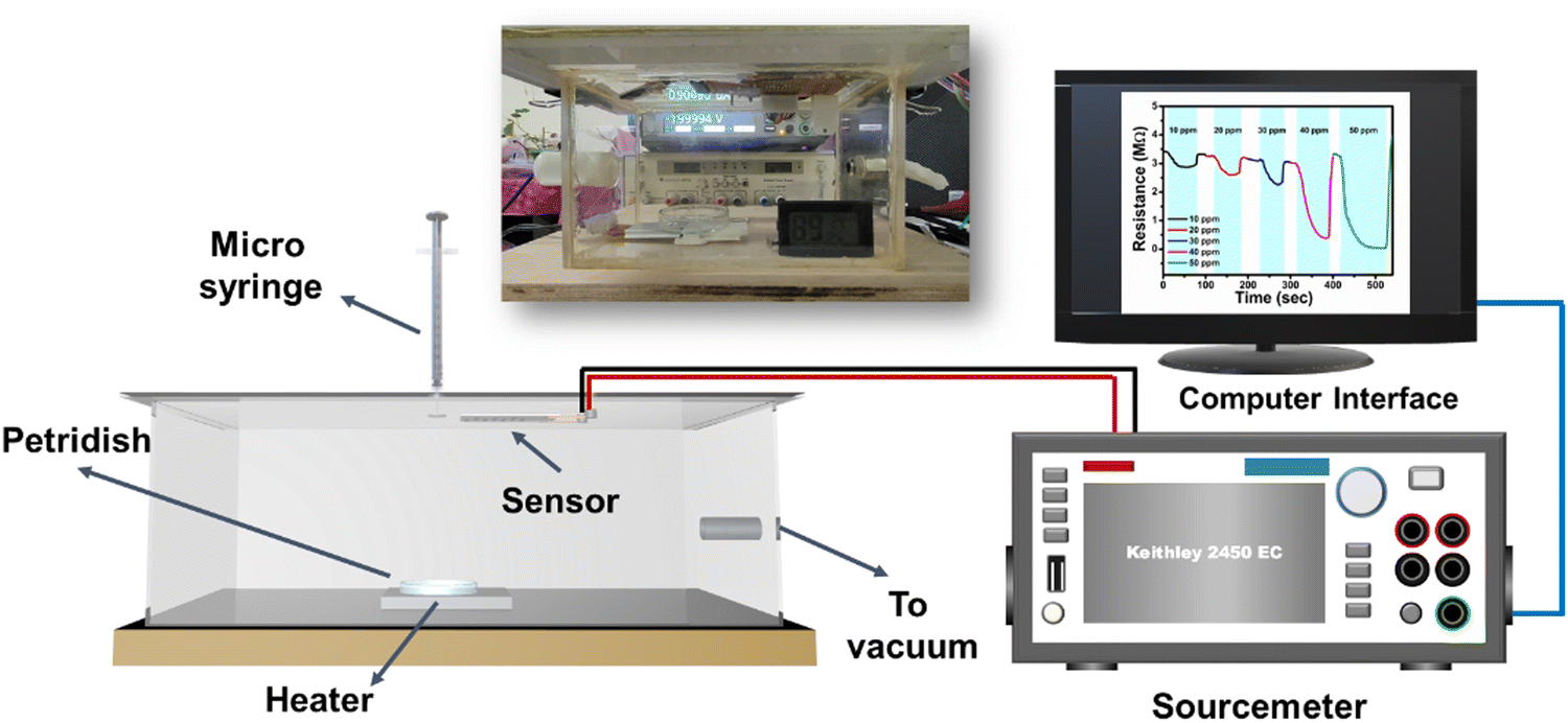 | ||
| Fig. 4 Schematic of the gas sensing setup assembly; inset: digital image of the sensing assembly. | ||
Fig. 5 shows the dynamic responses of the MoS2 and N-MoS2 sensors at room temperature towards ammonia (NH3), formaldehyde (HCHO), and triethylamine (TEA). Fig. 5(a) shows the responses of the MoS2 and N-MoS2 sensors to ammonia. N-MoS2 sensor exhibits an enhanced sensing response to NH3 compared to the MoS2 sensor. In contrast, in the case of HCHO and TEA (Fig. 5(b) and (c)), there is little change in the response. Fig. 5(d) shows a comparison histogram of the sensing responses of MoS2 and N-MoS2 towards NH3, HCHO and TEA, respectively. To check the selectivity of N-MoS2 sensor towards common interfering VOCs, acetone and ethanol were also exposed to measure the sensing response.
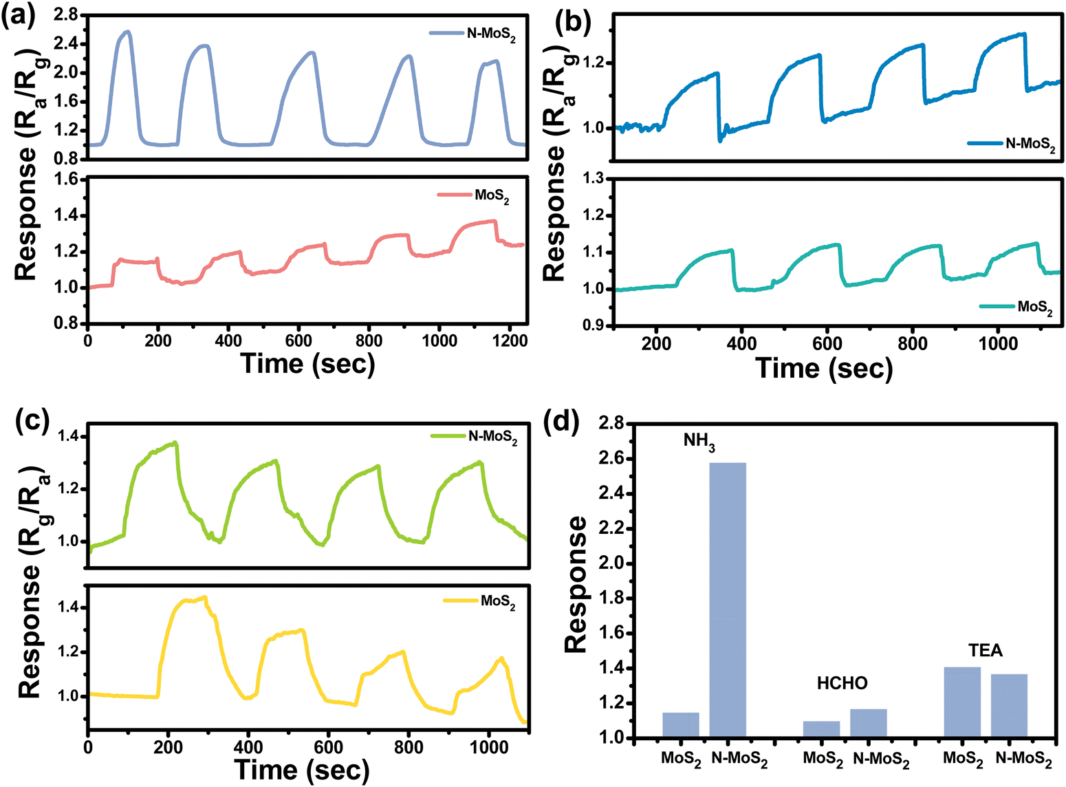 | ||
| Fig. 5 Dynamic sensing responses of the MoS2 and N-MoS2 sensors towards (a) NH3, (b) HCHO and (c) TEA at room temperature and (d) comparison of the sensing responses of MoS2 and N-MoS2 sensors towards various analyte VOCs. | ||
The effect of plasma exposure time on the sensing performance of the MoS2 nanoflower structure was analysed by exposing the nitrogen plasma at three different times (5 min, 10 min and 15 min). The sensing responses of the plasma-treated sensors and the non-treated MoS2 sensor (MS sensor) are shown in Fig. 6. The different plasma-treated sensors were termed NMS_05 (5 min plasma exposure), NMS_10 (10 min plasma exposure), and NMS_15 (15 min plasma exposure), depending on the plasma exposure time. The results show that NMS_05 exhibits no significant change in response compared with the MS sensor. However, NMS_10 and NMS_15 sensors have similar responses to 10 ppm NH3 vapour at room temperature.
 | ||
| Fig. 6 Dynamic sensing response of (a) MoS2 (MS sensor) and N-MoS2 sensors with different nitrogen plasma exposure times of (b) 5 min (NMS_05), (c) 10 min (NMS_10), and (d) 15 min (NMS_15) towards 10 ppm NH3 vapour. | ||
Fig. 7(a) shows the selectivity of the synthesized N-MoS2 sensor towards various VOCs. As shown in the figure, the sensor is highly selective towards NH3 compared to other common VOCs in the ambient environment. Fig. 7(b) shows the response and recovery times of N-MoS2 towards 10 ppm NH3 vapour. The response time of a sensor is the time taken for the resistance to reach 90% of its total change when the sensor is in the proximity of the target gas, while the recovery time is the duration needed for the resistance to return to 90% of its original baseline after the gas is removed.4,7 The response time of the sensor was 22 s, whereas the recovery time was 23 s.
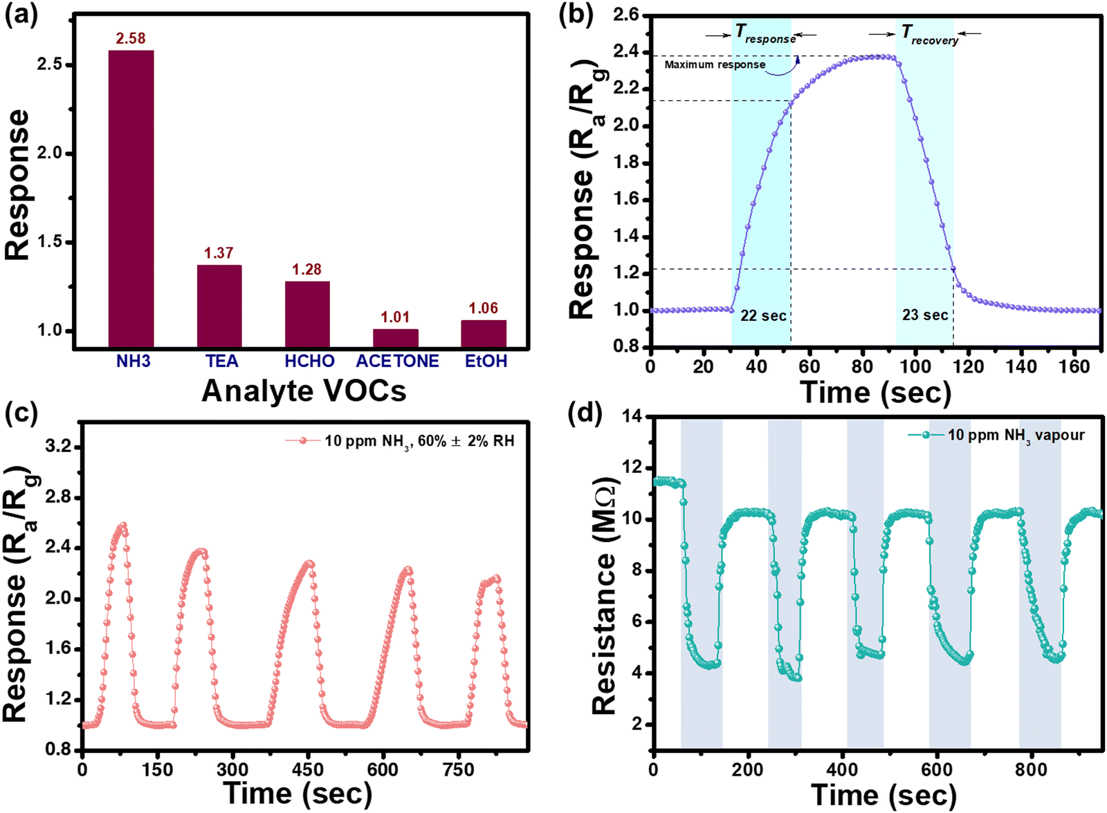 | ||
| Fig. 7 (a) Selectivity of N-MoS2 sensor towards different analyte VOCs; (b) response and recovery time measurements of N-MoS2 sensor; (c) dynamic sensing response of N-MoS2 sensor towards 10 ppm NH3; and (d) resistance change during the exposure of 10 ppm NH3 vapour to N-MoS2 sensor. | ||
The dynamic changes in the response of the sensor to 10 ppm NH3 vapour are shown in Fig. 7(c). Up to five cycles, the sensor showed an almost constant response with a little bit of deviation from the initial response. Fig. 7(d) shows the variation in sensor resistance towards 10 ppm NH3 vapour. The changes in the resistance values were almost constant from the baseline value, with a deviation at the initial cycle.
Fig. 8(a) shows the dynamic response of N-MoS2 sensor to varying NH3 concentrations during continuous measurement. The sensor has a very high response with increasing concentrations of the analyte vapour, which may be due to humidity. Fig. 8(b) shows the linear response with the fitting curve of N-MoS2 sensor to different VOC concentrations. From the calibration curve with increasing concentration of the NH3 vapour, it can be observed that the curve is statistically linear with a correlation coefficient value R2 = 0.97. The theoretical estimation of the limit of detection (LOD) of the sensor can be estimated using the following eqn (3):50
 | (3) |
 | (4) |
 | ||
| Fig. 8 (a) Response of N-MoS2 sensor to varying concentrations of NH3 in a continuous measurement; (b) linear response with fitting curve of N-MoS2 sensor to different VOC concentrations; (c) measurement of resistance changes from its baseline resistance with increasing concentration of analyte VOC at room temperature; and (d) variation in the baseline resistance of the sensor with varying relative humidity. | ||
Fig. 8(c) shows the dynamic resistance changes of N-MoS2 sensor with varying concentrations of NH3 vapour. The sensor is sensitive to humidity, and with an increase in the analyte VOC's volume, the humidity inside the chamber also increases, which enhances the sensor's response to high concentrations of NH3. Fig. 8(d) shows the variation in baseline resistance at different relative humidity values inside the sensing chamber at room temperature.
3.3. Computational analysis
For the computational analysis, a 4 × 4 × 1 supercell of MoS2 containing 48 atoms was used. In the equilibrium state, the Mo and S atoms of the MoS2 monolayer form a hexagonal lattice. The lattice constants of the MoS2 monolayer are a = 3.21 Å and c = 12.14 Å. The values are in good agreement with earlier experimental and theoretical results.51 To depict the incorporation of nitrogen and sulphur vacancy in the MoS2 monolayer, one sulphur atom was replaced by a nitrogen atom, and one sulphur atom was removed.The optimised geometrical configurations of nitrogen-incorporated MoS2 monolayers with sulfur vacancy and with different gases are presented in Fig. 8. All possible binding sites of the MoS2 monolayer were considered, and the configuration with the highest binding energy was considered in further calculations to reflect the most probable experimental scenario.
The binding energies of all gases in the nitrogen-incorporated MoS2 monolayer, as calculated using eqn (4), are shown in Fig. 9. The binding energy of the NH3 molecule with the nitrogen-incorporated MoS2 monolayer was the highest (−0.81 eV). The binding energy of the TEA molecule was the lowest (−0.18 eV). This finding is in close agreement with the sensing response of the nitrogen-incorporated MoS2 monolayer. To delve deeper into the interaction between the various gases and the nitrogen-incorporated MoS2 monolayer, a substantial charge transfer occurs between them, as shown in Fig. 9. In addition to the N-MoS2 system with S vacancy, the effect of NH3 adsorption on the N-MoS2 system without S vacancy was investigated. The charge density difference plots of all gases and the MoS2 and nitrogen-incorporated MoS2 monolayer without sulfur vacancies are shown in the ESI† (Fig. S3).
 | ||
| Fig. 9 Optimized configuration structures with electron charge density differences (EDDs) (Δρ) of N-MoS2 sample with S vacancy, along with intermolecular distances of N-MoS2 with various VOCs. The yellow colour corresponds to charge accumulations, and the cyan colour corresponds to charge depletion. | ||
Similarly, from the intermolecular distances between gas molecules and nitrogen-incorporated MoS2 monolayers with S vacancy, it was found that the NH3 molecule exhibited the lowest distance (3.2 Å), whereas the TEA molecule exhibited the highest distance of 8.5 Å. This result can be explained by the increased electrostatic interaction between the NH3 molecule and the nitrogen-incorporated MoS2 monolayer.
For comparison, the binding energy values of all three systems (i.e., only MoS2, N-MoS2 without S vacancy, and N-MoS2 with S vacancy) are summarized in Tables 1, 2 and 3, respectively.
| System | Adsorption energy (eV) | Intermolecular distance (Å) |
|---|---|---|
| MoS2 + ammonia | −0.38 | 5.2 |
| MoS2 + formaldehyde | −0.31 | 5.1 |
| MoS2 + TEA | −0.18 | 9.4 |
| MoS2 + ethanol | −0.27 | 5.8 |
| MoS2 + acetone | −0.35 | 5.5 |
| System | Adsorption energy (eV) | Intermolecular distance (Å) |
|---|---|---|
| MoS2 + ammonia | −0.76 | 3.9 |
| MoS2 + formaldehyde | −0.45 | 5.7 |
| MoS2 + TEA | −0.12 | 9.1 |
| MoS2 + ethanol | −0.53 | 4.7 |
| MoS2 + acetone | −0.42 | 5.2 |
| System | Adsorption energy (eV) | Intermolecular distance (Å) |
|---|---|---|
| MoS2 + ammonia | −0.81 | 3.2 |
| MoS2 + formaldehyde | −0.42 | 5.1 |
| MoS2 + TEA | −0.18 | 8.5 |
| MoS2 + ethanol | −0.61 | 4.1 |
| MoS2 + acetone | −0.55 | 4.5 |
To examine the changes in the electronic properties of the nitrogen-incorporated MoS2 monolayer upon NH3 molecule adsorption, the total density of states (TDOS) was plotted (Fig. 10). The adsorption of the NH3 molecule on the nitrogen-incorporated MoS2 monolayer leads to a significant shift in the Fermi level towards higher energy. This also introduces new peaks at the conduction band at 0.52 eV and 1.97 eV. This shows that the introduction of the NH3 molecule results in changes in the electronic properties of the nitrogen-incorporated MoS2 monolayer.
 | ||
| Fig. 10 Total density of state (TDOS) of the (a) MoS2 system with N attachment and N attachment with S vacancy before NH3 adsorption; (b) MoS2 upon NH3 molecule adsorption; (c) N-MoS2 without sulfur vacancy upon NH3 molecule adsorption; and (d) N-MoS2 with S vacancy upon NH3 molecule adsorption. | ||
To delve deeper into the mechanism behind the change in the density of the state of N-MoS2 after NH3 adsorption, we calculated the PDOS of N-MoS2 with a sulphur vacancy before NH3 adsorption and N-MoS2 with a sulphur vacancy after NH3 adsorption. From Fig. 11(a), it can be seen that the major contribution in the valence band near the Fermi level is from the dz2 orbital of molybdenum atoms, followed by a contribution from the pz orbital of sulphur atoms. In contrast, in the case of N-MoS2 with S vacancy after NH3 adsorption, the major contribution in the conduction band near the Fermi level is from the dx2−y2 orbital of Molybdenum atoms, followed by a contribution from the py orbital of sulphur atoms (Fig. 11(b)).
 | ||
| Fig. 11 Projected density of states (PDOS) of (a) N-MoS2 with S vacancy: before NH3 adsorption and (b) N-MoS2 with S vacancy: after NH3 adsorption. | ||
3.4. Gas sensing mechanism:
The sensing mechanism of N-MoS2 sensor is based on the change in the electrical resistance during the interaction of analyte vapour and the sensing material. Argon plasma treatment before nitrogen plasma may create sulfur vacancy due to the bombardment of energetic ions, contributing to the n-type characteristics of N-MoS2.52–54 Additionally, oxygen may get adsorbed on the sulfur vacancies, creating oxygen adsorbates, which may also contribute to the n-type behaviour of the sensor.55,56 Along with this, nitrogen plasma treatment may attach nitrogen to the MoS2, which enhances electron carrier concentration in MoS2 by introducing donor levels adjacent to the conduction band, hence augmenting n-type conductivity.57–59 Moreover, the incorporation of nitrogen can make the sensor exhibit a more stable response than a non-treated MoS2 sensor.60Fig. 12 shows the plausible sensing mechanism of N-MoS2 sensor towards NH3 vapours. | ||
| Fig. 12 (a) MoS2 sensor before plasma treatment; (b) Ar plasma treatment on the MoS2 sensor creating S vacancies; (c) N2 plasma treatment on the sensor with nitrogen attachments taking place at some vacancies; and (d) interaction of NH3 molecules with S vacancies and nitrogen attachment sites. | ||
The I–V characteristic plot (ESI,† Fig. S4) also shows an increase in current after plasma treatment, which is also an n-type behaviour of N-MoS2 sensor. When the NH3 molecules interact with the sensing material, electron transfer occurs from NH3 to the sensing material, which changes the resistance of the sensing material.4 Hence, plasma treatment can enhance the sensing capabilities of MoS2 sensors. The theoretical investigations are also consistent with the experimental results. Table 4 presents a comparison among various MoS2-based sensors modified by plasma treatment, as well as doping by chemical methods, with the work presented here.
| Sl no. | Title description | Targeted Gas/VOCs | Operating temperature | Limit of detection (LOD) | Response/recovery time | Ref. |
|---|---|---|---|---|---|---|
| 1 | Electronic modulation of MoS2 nanosheets via N-doping | NO2 | Room temperature | 62.5 ppb | 53 s/323 s (10 ppm) | 28 |
| 2 | Synergetic phase modulation and N-doping of MoS2 | NO2 | Room temperature | 0.13 ppm | 43.1 s/301.2 s (10 ppm) | 61 |
| 3 | Metal-doped MoS2 nanoflower | SO2 | Room temperature | 250 ppb | — | 62 |
| 4 | Zinc-doped MoS2/RGO composites | NH3 | 200 °C | 6 ppm | 21.3 s/44.9 s (50 ppm) | 63 |
| 5 | N dopant-triggered MoS2 nanosheets | NO2 | Room temperature | 125 ppb | 20 s/113 s (10 ppm) | 37 |
| 6 | Dual functionalized flower-like MoS2 nanospheres with Pd and g-C3N4 | TEA | 225 °C | 17 ppb | 38 s/26 s (30 ppm) | 64 |
| 7 | N-doped MoS2 hierarchical structures | NO2 | 25 °C | 10 ppb | 146 s/52 s (10 ppb) | 60 |
| 8 | Cu-functionalized MoS2 nanoworm thin films | NO2 | 100 °C | 2 ppm | 54 s/82 s | 65 |
| 9 | Co-incorporated MoS2 nanosheets | NO2 | Room temperature | 7 ppm | 10 s/600 s | 18 |
| 10 | DC Plasma-modified MoS 2 nanoflower | NH 3 | Room temperature | 80 ppb | 22 s/23 s | This Work |
4. Conclusion
In summary, we fabricated a nitrogen-incorporated MoS2 sensor following DC plasma treatment with a highly selective sensing response towards NH3 at room temperature. MoS2 was synthesized following a wet chemical approach following argon and nitrogen plasma treatment, which created sulfur vacancies and nitrogen incorporation into the MoS2 matrix. The XPS spectra of the plasma-treated sensor showed an increase in nitrogen content compared with the non-treated sample. Moreover, the FESEM images also show some deformation after plasma treatment. EDX spectra also show nitrogen content. Plasma treatment enhances the number of active sites on the MoS2 surface, which enhances the transfer of electrons from NH3 to the active sites and increases the sensing response of the sensor compared to the pristine MoS2 sensor. The sensor shows a fast response (22 s) and recovery time (23 s). The sensor also shows very selective detection of NH3 compared to other common toxic VOCs, with a limit of detection of 80 ppb. This DC plasma treatment method can be applied for the fabrication of very highly sensitive VOC sensors in a controllable manner.Author contributions
A. K. – conceptualization, methodology, investigation, formal analysis, visualization, data curation, and writing of the original draft. B. C. – methodology (theoretical), investigation, and writing – original draft. T. H. – methodology, investigation, data curation, and writing – original draft. S. C. – investigation, data curation. B. K. – resources, investigation, H. K. – resources, conceptualization, visualization, supervision, funding acquisition, and writing – review and editing*.Data availability
The data supporting this article have been included as part of the ESI.†Conflicts of interest
The authors declare no competing financial interest.Acknowledgements
The authors are thankful to Sophisticated Analytical Instrument Facility (SAIF) and Central Instrument Facility (CIF), Gauhati University (GU), IIT Guwahati, and National Chemical Laboratory, Pune for providing material characterization facilities. H. K. would like to thank DST-PURSE (SR/PURSE/2022/116), ISRO (RAC-S, GU/RAC-S/01/2020-21/03), and Joint Network Centre: Indo-South Korea joint project (INT/Korea/JNC/CPS, DST, Govt. of India, 2021–2024) for providing the financial support. A. K. would like to thank CSIR-HRDG for providing fellowship under the SRF-Direct Scheme. B. C. would like to thank the Department of Applied Sciences, GU, for providing the computation facility for the simulation.References
- S. Freddi, A. V. Emelianov, I. I. Bobrinetskiy, G. Drera, S. Pagliara, D. S. Kopylova, M. Chiesa, G. Santini, N. Mores, U. Moscato, A. G. Nasibulin, P. Montuschi and L. Sangaletti, Adv. Healthcare Mater., 2020, 9, 2000377 CrossRef CAS PubMed.
- L. Zhang, K. Khan, J. Zou, H. Zhang and Y. Li, Adv. Mater. Interfaces, 2019, 6, 1901329 CrossRef.
- V. Van Tran, D. Park and Y. C. Lee, Int. J. Environ. Res. Public Health, 2020, 17, 2927 CrossRef CAS PubMed.
- A. Kashyap, H. Sarma, B. Chakraborty and H. Kalita, ACS Appl. Electron. Mater., 2024, 6, 6916–6931 CrossRef CAS.
- K. Wang, L. Lee, S. L. Loo, T. Y. Yang, C. T. Chen, T. W. Kuo, J. L. Chen, H. C. Kuo and Y. L. Chueh, ACS Appl. Nano Mater., 2023, 6, 5336–5344 CrossRef CAS.
- W. C. Tan and K. W. Ang, Adv. Electron. Mater., 2021, 7, 1–21 CrossRef.
- A. Kashyap, B. Chakraborty, M. S. Siddiqui, H. Tyagi and H. Kalita, ACS Appl. Nano Mater., 2023, 6, 7948–7959 CrossRef CAS.
- S. Acosta and M. Quintana, Sensors, 2024, 24, 1817 CrossRef CAS PubMed.
- H. Schmidt, F. Giustiniano and G. Eda, Chem. Soc. Rev., 2015, 44, 7715–7736 RSC.
- W. Zheng, X. Liu, J. Xie, G. Lu and J. Zhang, Coord. Chem. Rev., 2021, 447, 214151 CrossRef CAS.
- A. Shokri and N. Salami, Sens. Actuators, B, 2016, 236, 378–385 CrossRef CAS.
- J. Chen and W. Xu, eScience, 2023, 3, 100178 CrossRef.
- P. Li, G. Zhang, Z. Kang, X. Zheng, Y. Xie, C. Liang, Y. Zhang, X. Fang, R. Sun, Z. Liu, Y. Bu, Y. Lu and Y. Zhang, InfoMat, 2023, 5, e12457 CrossRef CAS.
- R. Duan, W. Qi, K. Tang and W. Liu, InfoMat, 2025, 7, e12610 CrossRef CAS.
- J. Zhao, Z. Chen, S. Liu, P. Li, S. Yu, D. Ling and F. Li, BMEMat, 2024, 2, e12066 CrossRef CAS.
- L. Luo, J. Gao, L. Zheng, L. Li, W. Li, M. Xu, H. Jiang, Y. Li, H. Wu, H. Ji, X. Dong, R. Zhao, Z. Liu, X. Wang and W. Huang, InfoMat, 2024, 6, e12605 CrossRef CAS.
- L. Chacko, E. Massera and P. M. Aneesh, J. Electrochem. Soc., 2020, 167, 106506 CrossRef CAS.
- P. Bharathi, S. Harish, M. Shimomura, S. Ponnusamy, M. Krishna Mohan, J. Archana and M. Navaneethan, Sens. Actuators, B, 2022, 360, 131600 CrossRef CAS.
- P. Bharathi, S. Harish, G. Mathankumar, M. Krishna Mohan, J. Archana, S. Kamalakannan, M. Prakash, M. Shimomura and M. Navaneethan, Appl. Surf. Sci., 2022, 600, 154086 CrossRef CAS.
- D. Zhang, Z. Yang, P. Li, M. Pang and Q. Xue, Nano Energy, 2019, 65, 103974 CrossRef CAS.
- M. Ikram, L. Liu, H. Lv, Y. Liu, A. Ur Rehman, K. Kan, W. J. Zhang, L. He, Y. Wang, R. Wang and K. Shi, J. Hazard. Mater., 2019, 363, 335–345 CrossRef CAS PubMed.
- K. Rathi and K. Pal, Adv. Mater. Interfaces, 2020, 7, 2000140 CrossRef CAS.
- Y. Liang, L. Zhang, K. Wang, J. Ren, L. Yu and M. Yin, Sens. Actuators, B, 2023, 378, 133137 CrossRef CAS.
- J. Le Fan, X. F. Hu, W. W. Qin, M. Zhou, Y. S. Liu, S. Cheng, S. J. Gao, L. P. Tan, G. Q. Wang and W. Zhang, J. Mater. Chem. C, 2023, 11, 2364–2374 RSC.
- Z. Sheng, P. Qi, Y. Lu, G. Liu, M. Chen, X. Gan, Y. Qin, K. Hao and Y. Tang, ACS Appl. Mater. Interfaces, 2021, 13, 34495–34506 CrossRef CAS PubMed.
- P. Tao, J. He, T. Shen, Y. Hao, J. Yan, Z. Huang, X. Xu, M. Li and Y. Chen, Adv. Mater. Interfaces, 2019, 6, 1900460 CrossRef.
- S. Deng, Y. Zhong, Y. Zeng, Y. Wang, Z. Yao, F. Yang, S. Lin, X. Wang, X. Lu, X. Xia, J. Tu, S. J. Deng, Y. Zhong, Z. J. Yao, X. L. Wang, X. H. Xia, J. P. Tu, Y. X. Zeng, X. H. Lu, Y. D. Wang, F. Yang and S. W. Lin, Adv. Mater., 2017, 29, 1700748 CrossRef PubMed.
- K. Zhao, X. Chang, J. Zhang, F. Yuan and X. Liu, ACS Sens., 2024, 9, 388–397 CrossRef CAS PubMed.
- A. E. Abusrafa, S. Habib, I. Krupa, M. Ouederni and A. Popelka, Coatings, 2019, 9, 145 CrossRef.
- C. Ma, A. Nikiforov, D. Hegemann, N. De Geyter, R. Morent and K. Ostrikov, Int. Mater. Rev., 2023, 68, 82–119 CrossRef CAS.
- R. V. Dabhade, D. S. Bodas and S. A. Gangal, Sens. Actuators, B, 2004, 98, 37–40 CrossRef CAS.
- S. Dou, L. Tao, R. Wang, S. El Hankari, R. Chen and S. Wang, Adv. Mater., 2018, 30, 1705850 CrossRef PubMed.
- X. Ji, X. Yuan, J. Wu, L. Yu, H. Guo, H. Wang, H. Zhang, D. Yu and Y. Zhao, ACS Appl. Mater. Interfaces, 2017, 9, 24616–24624 CrossRef CAS PubMed.
- T. Hazarika, B. Kakati, D. Pal, R. Saikia, A. Rawal, M. K. Mahanta and S. Biswas, Sci. Rep., 2024, 14, 1–23 CrossRef PubMed.
- L. Tao, X. Duan, C. Wang, X. Duan and S. Wang, Chem. Commun., 2015, 51, 7470–7473 RSC.
- A. Azcatl, X. Qin, A. Prakash, C. Zhang, L. Cheng, Q. Wang, N. Lu, M. J. Kim, J. Kim, K. Cho, R. Addou, C. L. Hinkle, J. Appenzeller and R. M. Wallace, Nano Lett., 2016, 16, 5437–5443 CrossRef CAS PubMed.
- R. Wu, J. Hao, S. Zheng, Q. Sun, T. Wang, D. Zhang, H. Zhang, Y. Wang and X. Zhou, Appl. Surf. Sci., 2022, 571, 151162 CrossRef CAS.
- T. Hazarika, P. Das, J. Jose, B. Kakati, D. Pal, R. Saikia and M. K. Mahanta, Polym. Adv. Technol., 2023, 34, 2862–2878 CrossRef CAS.
- S. J. Clark, M. D. Segall, C. J. Pickard, P. J. Hasnip, M. I. J. Probert, K. Refson and M. C. Payne, Z. Kristallogr., 2005, 220, 567–570 CAS.
- C. Yang, Z. Y. Zhao, H. T. Wei, X. Y. Deng and Q. J. Liu, RSC Adv., 2021, 11, 4276–4285 RSC.
- J. P. Perdew, K. Burke and M. Ernzerhof, Phys. Rev. Lett., 1996, 77, 3865 CrossRef CAS PubMed.
- S. Grimme, J. Comput. Chem., 2006, 27, 1787–1799 CrossRef CAS PubMed.
- T. H. Fischer and J. Almlöf, J. Phys. Chem., 1992, 96, 9768–9774 CrossRef CAS.
- S. Y. Cho, H. J. Koh, H. W. Yoo, J. S. Kim and H. T. Jung, ACS Sens., 2017, 2, 183–189 CrossRef CAS PubMed.
- Z. Chen, D. Yin and M. Zhang, Small, 2018, 14, 1703818 CrossRef PubMed.
- Y. Zhang, Y. Jiang, Z. Duan, Y. Wu, Q. Zhao, B. Liu, Q. Huang, Z. Yuan, X. Li and H. Tai, J. Hazard. Mater., 2022, 434, 128836 CrossRef CAS PubMed.
- L. Feng, L. Zhang, S. Zhang, X. Chen, P. Li, Y. Gao, S. Xie, A. Zhang and H. Wang, ACS Appl. Mater. Interfaces, 2020, 12, 17547–17556 CrossRef CAS PubMed.
- F. Y. Meng, H. Wu, M. Qiao, X. F. Zeng, D. Wang and J. X. Wang, Langmuir, 2022, 38, 1567–1577 CrossRef CAS PubMed.
- L. Lin, Z. K. Yang, Y. F. Jiang and A. W. Xu, ACS Catal., 2016, 6, 4449–4454 CrossRef CAS.
- D. Liu, J. Pan, J. Tang, W. Liu, S. Bai and R. Luo, J. Phys. Chem. Solids, 2019, 124, 36–43 CrossRef CAS.
- E. S. Kadantsev and P. Hawrylak, Solid State Commun., 2012, 152, 909–913 CrossRef CAS.
- J. He, Y. Wen, D. Han, P. Zeng, P. Zheng, L. Zheng, W. Su, Z. Wu and Y. Zhang, Mater. Sci. Semicond. Process., 2023, 158, 107347 CrossRef CAS.
- K. Cho, M. Min, T. Y. Kim, H. Jeong, J. Pak, J. K. Kim, J. Jang, S. J. Yun, Y. H. Lee, W. K. Hong and T. Lee, ACS Nano, 2015, 9, 8044–8053 CrossRef CAS PubMed.
- H. Qiu, T. Xu, Z. Wang, W. Ren, H. Nan, Z. Ni, Q. Chen, S. Yuan, F. Miao, F. Song, G. Long, Y. Shi, L. Sun, J. Wang and X. Wang, Nat. Commun., 2013, 4, 1–6 Search PubMed.
- A. Wu, Q. Song and H. Liu, Comput. Theor. Chem., 2020, 1187, 112906 CrossRef CAS.
- G. Sun, F. Li, T. Wu, L. Cong, L. Sun, G. Yang, H. Xie, A. Mauger, C. M. Julien and J. Liu, Inorg. Chem., 2019, 58, 2169–2176 CrossRef CAS PubMed.
- A. A. Kotsun, V. A. Alekseev, S. G. Stolyarova, A. A. Makarova, M. A. Grebenkina, A. P. Zubareva, A. V. Okotrub and L. G. Bulusheva, J. Alloys Compd., 2023, 947, 169689 CrossRef CAS.
- Q. Yang, Z. Wang, L. Dong, W. Zhao, Y. Jin, L. Fang, B. Hu and M. Dong, J. Phys. Chem. C, 2019, 123, 10917–10925 CrossRef CAS.
- M. W. Jung, W. Song, D. S. Jung, S. S. Lee, C. Y. Park and K. S. An, J. Nanosci. Nanotechnol., 2016, 16, 2756–2759 CrossRef CAS PubMed.
- M. Yin, K. Wang, C. Gao, R. Yang, Y. Huang and L. Yu, Mater. Res. Bull., 2024, 179, 112943 CrossRef CAS.
- J. Kim, M. Li, C. H. Lin, L. Hu, T. Wan, A. Saeed, P. Guan, Z. Feng, T. Kumeria, J. Tang, D. Su, T. Wu and D. Chu, Adv. Sci., 2025, 12, 2410825 CrossRef CAS PubMed.
- D. Zhang, J. Wu, P. Li and Y. Cao, J. Mater. Chem. A, 2017, 5, 20666–20677 RSC.
- S. P. Linto Sibi, M. Rajkumar, K. Govindharaj, J. Mobika, V. Nithya Priya and R. T. Rajendra Kumar, Anal. Chim. Acta, 2023, 1248, 340932 CrossRef CAS PubMed.
- W. Guo, K. Chen, S. Wang, H. Zhang and D. Wu, Sens. Actuators, B, 2025, 433, 137490 CrossRef CAS.
- S. Tyagi, A. Kumar, A. Kumar, Y. K. Gautam, V. Kumar, Y. Kumar and B. P. Singh, Mater. Res. Bull., 2022, 150, 111784 CrossRef CAS.
Footnote |
| † Electronic supplementary information (ESI) available. See DOI: https://doi.org/10.1039/d5ma00232j |
| This journal is © The Royal Society of Chemistry 2025 |