DOI:
10.1039/D3QI02132G
(Research Article)
Inorg. Chem. Front., 2024,
11, 409-416
Molecular insight into intrinsic-trap-mediated emission from atomically precise copper-based chalcogenide models†
Received
17th October 2023
, Accepted 17th November 2023
First published on 17th November 2023
Abstract
Luminescent Cu-doped semiconductor nanocrystals have long played a pivotal role in the advancement of lighting and display technologies. The luminescence observed in colloidal copper-based I–III–VI nanocrystals is attributed to defect emission arising from donor–acceptor pair recombination of excited charge carriers. However, a detailed atomic-level exploration of how distinct chemical components precisely influence the defect position has remained challenging, primarily due to inherent local structural imprecision of the traditional I–III–VI nanocrystals. In this study, we have prepared a set of copper-containing I–III–VI metal chalcogenide nanoclusters, 1-CuInS, 1-CuGaS, and 2-CuGaS, serving as unique models to address the aforementioned issues. Interestingly, despite possessing an identical crystalline structure, 1-CuInS and 1-CuGaS exhibit significantly different photoluminescence behaviors. For comparsion, 1-CuGaS and 2-CuGaS, which share the same second building units but differ in structural configuration, demonstrate similar luminescence performance. More importantly, we found that the green emission observed in 1-CuInS likely stems from the radiative recombination of electrons migrating from shallow delocalized traps to copper-localized holes. In contrast, the red emission observed in both 1-CuGaS and 2-CuGaS is presumably due to the recombination of electrons originating from deeply localized traps with copper-localized holes. This disparity in trap sites appears to be highly dependent on the presence of trivalent metal ions (In3+ and Ga3+) within the clusters, and the hypothesis is further substantiated through photoluminescence characterization of 1-CuInGaS containing both In3+ and Ga3+ ions simultaneously. Furthermore, we have explored the impact of introducing Cd ions into 1-CuInS, which can alter the position of shallow delocalized traps and thereby fine-tune the luminescence properties. Our findings shed light on the intricate interplay of chemical composition and defect states in copper-containing I–III–VI nanoclusters, offering valuable insights into the optoelectronic properties of copper-based semiconductor nanocrystals.
Introduction
Metal chalcogenide semiconductor nanocrystals, also referred to as quantum dots (QDs), have captivated the scientific and technological community over the past few decades due to their intriguing photoluminescence (PL) properties.1–5 Among these, copper-based I–III–VI nanocrystals have garnered particular interest, attributable to their photophysical characteristics, such as optically activated copper midgap states, tuneable photoluminescence (PL) behavior across the visible and near-infrared (NIR) spectral range, and a composition free from toxic elements such as Cd or Pb,6–10 making them promising substitutes for most II–VI and IV–VI nanocrystals. Consequently, these nanocrystals hold potential applications in light-emitting diodes, nonlinear optics, and biomedical labeling.11–14 In this regard, extensive research efforts have been dedicated to unfolding the luminescence mechanisms and investigating the factors that influence the properties of copper-based I–III–VI nanocrystals, with the aim of enhancing their optoelectronic performance and further applications.
In general, the luminescence observed in copper-based I–III–VI nanocrystals serves as a quintessential example of the donor–acceptor pair (DAP) emission mechanism, which is related to the recombination of excitons, where electrons located in inherent defect sites situated below the conduction band act as donor states, and holes trapped in Cu vacancy (VCu).2,6,15,16 Previous efforts have demonstrated that both the composition and surface structure of these nanocrystals play a crucial role in determining the location and types of intrinsic defects, exerting a significant influence on the emission performance.15,17,18 However, despite special emphasis has been placed on understanding the defect-induced luminescence of I–III–VI nanocrystals, the correlations between chemical components and defect positions have yet to be systematically explored, primarily due to the inherent uncertainties of the atomic position in typical I–III–VI nanocrystals. Furthermore, the size inhomogeneity of QDs also presents challenges in elucidating the mechanism behind defect-mediated emission.
In this aspect, metal chalcogenide supertetrahedral nanoclusters (Tn, n indicates the number of metal layers along the edge of the tetrahedron) with precisely defined compositions and uniform sizes could serve as excellent model system to solve the above issue (Scheme 1).19–29 In previous study, Mn-related emission have been studied in detail in Mn based II–III–VI supertetrahedral nanoclusters. For instance, our investigations have delved into the role of dipole–dipole interactions directed by Mn–Mn distances in controlling Mn-related emissions through the examination of three structurally well-defined Mn-based II–III–VI supertetrahedral nanoclusters (MCOF-5, MCOF-6, and MCOF-7).30 In contrast, there has been a relative scarcity of investigation into the luminescence mechanism of copper-related emission from Cu-based I–III–VI supertetrahedral nanoclusters.31–34
 |
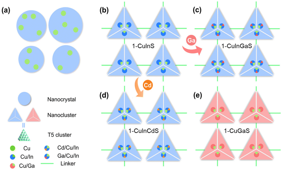
| | Scheme 1 (a) Cu-based classical I–III–VI nanocrystals with imprecise sites of Cu ions and inhomogeneous particle sizes. Copper-based chalcogenide supertetrahedral nanoclusters including (b) 1-CuInS, (c) 1-CuInGaS, (d) 1-CuInCdS, and (e) 1/2-CuGaS with relatively precise sites of Cu ions and homogeneous cluster size. | |
Herein, a series of copper-based I–III–VI metal chalcogenides (1-CuInS, 1-CuGaS, and 2-CuGaS) were synthesized and their photoluminescence behaviors were found strongly depend on the specific components present. Specifically, both 1-CuInS and 1-CuGaS are constructed by the assembly of supertetrahedral T5-Cu5M30S56 clusters which are linked by [MSb4S10] units (M = In for 1-CuInS and M = Ga for 1-CuGaS). In contrast, 2-CuGaS adopts the same second building units (SBUs) as 1-CuGaS but utilizes [SbS3] units as linkers. Interestingly, at room temperature, 1-CuInS emits green luminescence, whereas 1-CuGaS and 2-CuGaS only emit red luminescence at low temperatures. Temperature-dependent PL and PL decay dynamics analysis indicated that the green emission originates from shallow delocalized traps while the red emission arises from deep localized traps, and both resulting in radiative recombination with Cu vacancy acceptor. Additionally, the emission of 1-CuInS could be finely tuned through doping cadmium ions in the parent clusters due to the modulating of the position of the shallow delocalized traps.
Results and discussion
Synthesis and characterization of 1-CuInS, 1-CuGaS, and 2-CuGaS
Crystalline samples discussed here were synthesized via a similar solvothermal method with different types of protonated organic amines as templates (see the ESI† for more details). Their crystalline structures were determined by single-crystal X-ray diffraction (SCXRD), and compositions were further confirmed by energy dispersive X-ray spectroscopy (EDS) and elemental analysis (EA) (Fig. S1–S3†). In addition, the phase purity and thermal stability of the as-synthesized samples were characterized by powder X-ray diffraction (PXRD) (Fig. S4–S6†) and thermal gravimetric analysis (TGA) (Fig. S7–S9†), respectively. Furthermore, X-ray photoelectron spectroscopy (XPS) confirmed that Cu atoms in all the three structures were monovalent (Fig. S10†).
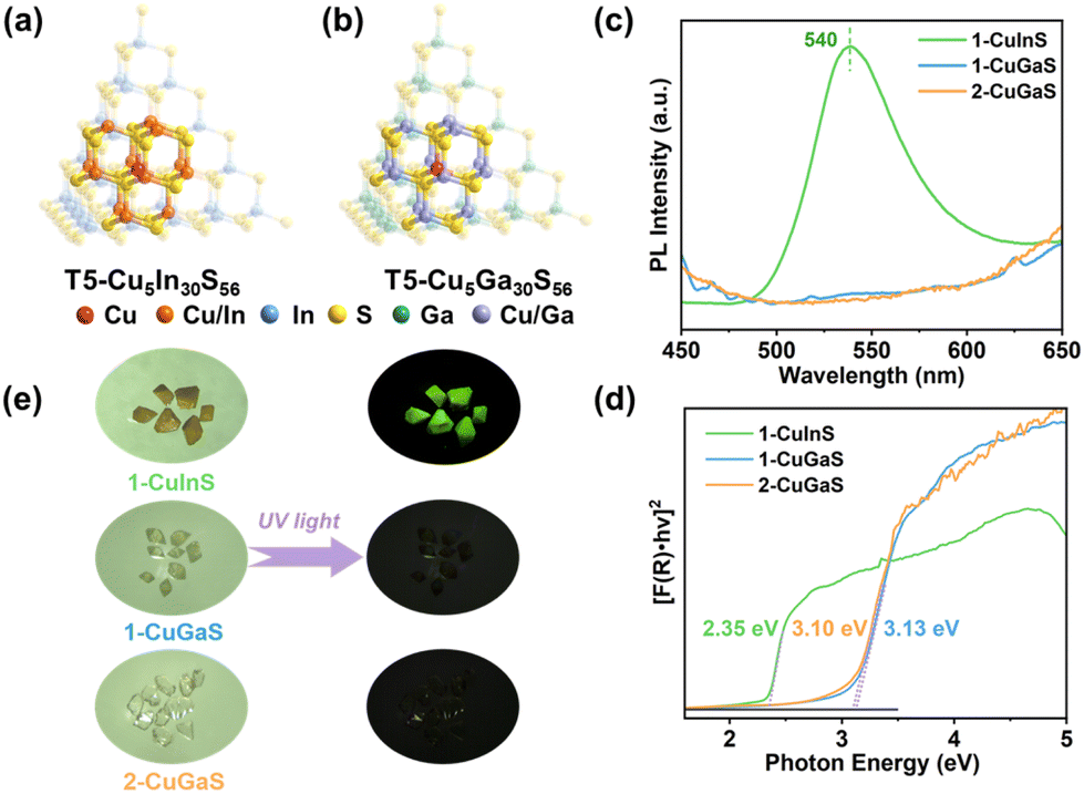
SCXRD analysis indicates that 1-CuInS and 1-CuGaS crystallize in the same space group tetragonal I41/a with very similar unit cell parameters while 2-CuGaS crystallizes in the hexagonal space group P63/m (Table S1†). The structures of 1-CuInS and 1-CuGaS are isomorphic, characterized by the assembly of supertetrahedral T5-Cu5M30S56 clusters linked by [MSb4S10] units (M = In for 1-CuInS and M = Ga for 1-CuGaS) (Fig. 1a and b). At the center of the linker is the tetrahedral [MS4] unit, which is further connected with four trigonal-pyramidal [SbS3] units through corner sulfurs, resulting in the formation of a [MSb4S10] unit with windmill shape when viewed along the c axis (Fig. S11†). Each [MSb4S10] unit joins for four T5-Cu5M30S56 cluster through corner-shared μ-S2− and vice versa, creating a double-interpenetrated framework with diamond topology (Fig. S12a, S12b, and S13a†). For 2-CuGaS, it possesses the same second building units (SBUs) as 1-CuGaS but with different linkers (Fig. 1b). Each [SbS3] linker in 2-CuGaS bridges three T5-Cu5Ga30S56 clusters and each T5-Cu5Ga30S56 connects to four neighboring clusters by four [SbS3] units, which give rise to a two-dimensional honeycomb (hcb) net (Fig. S12c and S13b†).
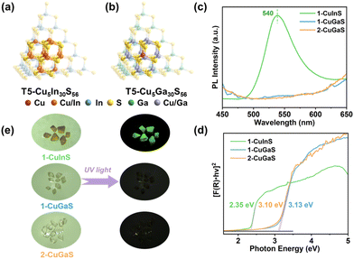 |
| | Fig. 1 (a) Supertetrahedral [Cu5In30S56] cluster in 1-CuInS. (b) Supertetrahedral [Cu5Ga30S56] clusters in 1-CuGaS. (c) RT PL spectra of 1-CuInS, 1-CuGaS, and 2-CuGaS. (d) Tauc plots of 1-CuInS, 1-CuGaS, and 2-CuGaS derived from UV-Vis DRS. (e) The optical images of pristine crystals with and without irradiation of an UV lamp. | |
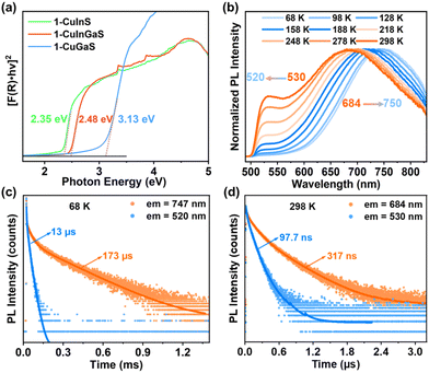
Interestingly, despite bearing similar supertetrahedral T5-Cu5M30S56 units, the three crystalline samples exhibit distinct photoluminescence properties. As illustrated in Fig. 1c, 1-CuInS displayed a strong green emission peak at 540 nm with a broad full width at half-maximum (fwhm) of 0.242 eV under excitation of 420 nm at room-temperature (RT). However, the luminescence of 1-CuGaS and 2-CuGaS was negligible at RT (Fig. 1e). The observation of green emission in 1-CuInS is reminiscent of the so-called copper “green” (“G-Cu”) luminescence in many Cu+-doped semiconductors with different compositions.35 In addition, the UV-Vis diffuse-reflectance spectra of the three samples were measured. As indicated in Fig. 1d, 1-CuInS, 1-CuGaS and 2-CuGaS were semiconductors, and their corresponding band gaps were detected to be 2.35 eV, 3.13 eV, and 3.10 eV, respectively. Ultraviolet photoemission spectroscopy (UPS) measurements revealed that they had a similar valence band position (5.14 eV for 1-CuInS; 5.10 eV for 1-CuGaS, and 4.97 eV for 2-CuGaS) (Fig. S14a†). Notably, 1-CuInS and 1-CuGaS displayed conspicuously different photoluminescence performances although they possessed identical frameworks and with different chemical compositions in the T5 SBUs. Conversely, 1-CuGaS and 2-CuGaS with the same SBUs both exhibited no emission at RT. These findings have spurred our interest for further research.
Temperature-dependent PL property of 1-CuInS, 1-CuGaS, and 2-CuGaS
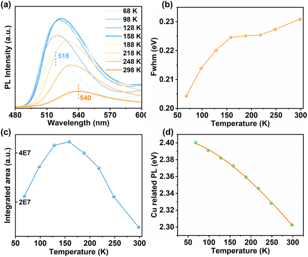
To uncover the mechanism behind Cu-related emission, temperature-dependent PL spectra were performed on these crystalline samples. Fig. 2a displays the temperature-dependent PL spectra of 1-CuInS. Upon cooling from 308 to 68 K, the emission peak wavelength (λmax) gradually blue-shifted from 541 nm to 518 nm, accompanied by a slight reduction in the PL fwhm from 0.231 eV to 0.204 eV (Fig. 2b). Meanwhile, the maximum excitation wavelength shifted from 504 nm to 486 nm according to PLE spectra (Fig. S15a†). Furthermore, we obtained the integrated PL data in Fig. 2a to illustrate the relationship between PL intensity and temperatures, as demonstrated in Fig. 2c. As the temperature decreased, the PL intensity of 1-CuInS increased non-monotonically. The initial increase in PL intensity from 308 to 158 K was mainly due to the suppression of non-radiative recombination pathways. However, the following decrease in PL intensity from 158 to 68 K is rather anomalous. The emission peak wavelength blue-shifts as the temperature decreases, ruling out the possibility of thermally activated delayed luminescence but suggesting negative thermal quenching (NTQ). NTO is an occasional phenomenon, which has been observed previously in defect emission.36 It is generally been explained by thermally activated carrier transfer from lower- to higher-energy emissive electron traps. Fig. 2d plots the energy of the Cu-related emission peak versus temperature. The orange solid line represents the fitting of these temperature-dependent peak energies to the Varshni equation:
where Eg is the energy gap in semiconductors, E0 represents its value at 0 K, and α, β are constants.16,37,38 The values were found [E0 = 2.41 eV, α = (10.1 ± 1.98) × 10−4 eV K−1, β = (5.58 ± 1.73) × 102 K] with R2 equal to 0.999. The good agreement provided strong support for the associations between the copper-related PL of 1-CuInS and the shallow delocalized traps, which vary with the position of the conduction band. A similar model has been proposed for bulk ZnS![[thin space (1/6-em)]](https://www.rsc.org/images/entities/char_2009.gif) :Cu,39 where the green emission originates from shallow delocalised traps, and the slight red shift of this emission was correlated with the shift of the conduction band to lower energies with increasing temperature.
:Cu,39 where the green emission originates from shallow delocalised traps, and the slight red shift of this emission was correlated with the shift of the conduction band to lower energies with increasing temperature.
 |
| | Fig. 2 Temperature-dependent PL properties of 1-CuInS: (a) PL spectra under different temperatures. (b) Fwhm of the Cu-related green emission. (c) PL-integrated areas of different emission. (d) Plot of the energies of PL peaks versus temperature. The orange solid line represents fits of the data to the Varshni equation. | |
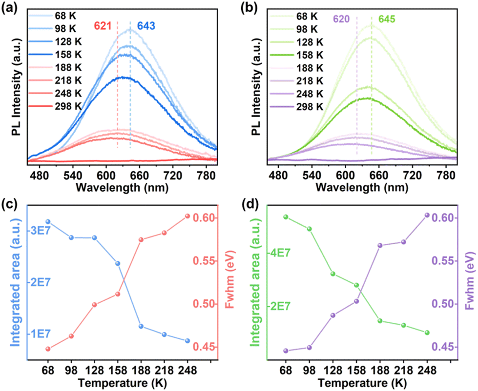
Unexpectedly, although 1-CuGaS and 2-CuGaS exhibited almost no emission at RT, both were able to emit Cu+-related red luminescence at lower temperatures. When cooling from 248 K to 68 K, the emission peak of 1-CuGaS gradually red-shifted from 621 nm to 643 nm and the emission intensity was remarkably increased (Fig. 3a). Notably, the maximum excitation wavelength showed negligible shifts during this process (Fig. S15b†). Similarly, the temperature-dependent PLE spectra of 2-CuGaS demonstrated that the maximum excitation wavelength remained unchanged as the temperature decreased (Fig. S15c†). Also, 2-CuGaS exhibited a similar redshift of emission peak and an increase in emission intensity with decreasing temperature (Fig. 3b). It is worth noting that, in comparison to 1-CuInS, both 1-CuGaS and 2-CuGaS have larger optical band gaps and emit longer wavelength emissions, resulting in a larger Stokes shift. The redshift of the emission peak with the decrease of temperature in 1-CuGaS and 2-CuGaS suggests that the radiative recombination is less associated with shallow delocalised traps and could be explained by processes related to deeply-localized-traps. In such a situation, the excited state occupies lower vibration levels with temperature decreasing, leading to the redshift of the emission spectra.35 Moreover, as depicted in Fig. 3c and d, the change of PL fwhm with temperature in 1-CuGaS and 2-CuGaS was comparable but much greater than that in 1-CuInS. In all, the emission peak of 1-CuInS shifted to higher energies with a decrease in temperature, accompanied by a slight reduction of half-widths. In contrast, the emission peaks of 1-CuGaS and 2-CuGaS shifted towards lower energies as the temperature decreased and half-widths of the spectra reduced significantly. Such differences in PL properties have been documented in cases involving different traps inducing copper-related emissions in Cu-based QDs.35,40 More importantly, it is reasonable to conclude that the position of trap sites is closely related to the local surroundings (In3+ and Ga3+ ions) rather than the structural patterning modes of these structures.
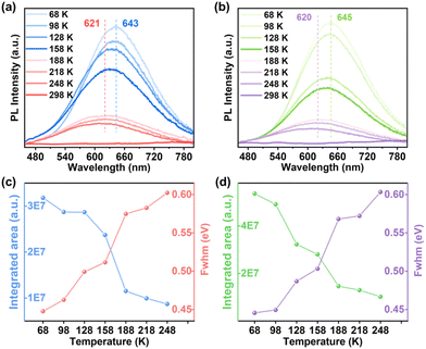 |
| | Fig. 3 Temperature-dependent PL spectra of (a) 1-CuGaS and (b) 2-CuGaS. PL-integrated areas and fwhm of (c) 1-CuGaS and (d) 2-CuGaS at different temperatures. | |
PL decay dynamics of 1-CuInS, 1-CuGaS and 2-CuGaS
To investigate the origin of the green and red emissions in more detail, temperature-dependent excited-state lifetime of 1-CuInS, 1-CuGaS, and 2-CuGaS were also recorded. As the temperature decreased, the PL decay time of 1-CuInS increased from 128 ns at 298 K to 7.2 μs at 68 K, which was ascribed to the decrement of non-radiative pathways (Fig. 4a and b; Tables S2 and S3†). In comparison, 1-CuGaS and 2-CuGaS exhibited significantly longer decay lifetimes. These values reached approximately 158 μs for 1-CuGaS and 214 μs for 2-CuGaS at 68 K (Fig. 4c, d, and S16; Tables S4 and S5†). Normally, the lifetime of band edge emission in various semiconductor nanocrystals falls in the range of one to a few tens of nanoseconds, which is not the case in the present work. These indicate that the emission of all the three samples is expected to originate from dopant related channels, similar to many Cu-doped nanocrystals.41 In addition, the literature suggests that the formation of long-lived photogenerated states in copper-doped nanocrystals, lasting from tens to hundreds of microseconds, is presumably associated with carrier localization at deep localised traps.35 Wherein, the shallow-delocalized traps of 1-CuInS and the deep-localized traps of 1-CuGaS and 2-CuGaS could also be reasonably explained. Furthermore, the gradual decrease in the average lifetime of both crystals with increasing temperature can be attributed to the increased occurrence of non-radiative pathways.
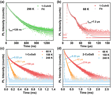 |
| | Fig. 4 PL decay curves of 1-CuInS measured at (a) 298 K and (b) 68 K. Temperature-dependent PL decay curves of (c) 1-CuGaS and (d) 2-CuGaS. | |
Optical band gap and PL property of 1-CuInGaS
Based on the above results, trivalent metal ions (In3+ and Ga3+) have indeed influence on the position of trap sites, further regulating the PL performance. To validate this hypothesis, we intentionally introduced Ga ions into 1-CuInS and obtained 1-CuInGaS. PXRD analysis confirmed the successful incorporation of Ga3+ ions into 1-CuInGaS, causing a slight shift in peak position due to the partial replacement of In3+ by Ga ions (Fig. S17†). EDS data indicated that the ratio of Ga to In is about 1:2 in a SBU (Fig. S18†). As illustrated in Fig. 5a, 1-CuInGaS has a band gap of 2.48 eV, which falls between the values of 1-CuInS and 1-CuGaS. Interestingly, under excitation of 450 nm at RT, 1-CuInGaS exhibited dual emissions in a high-energy band (530 nm) and low-energy band (684 nm) (Fig. S19†). Notably, the high-energy band showed a blue-shift tendency with decreasing temperature, while the low-energy band displayed a red-shift tendency (Fig. 5b and S20†). Furthermore, the decay lifetime of low-energy band was much longer than that of high-energy band at both 68 K and 298 K (Fig. 5c and d; Tables S6 and S7†). In this case, the high-energy band emission in 1-CuInGaS may result from the In3+ induced shallow-delocalized-traps to copper-localized hole transitions, while the low-energy band emission can be ascribed to the Ga3+ mediated deep-localized-traps to copper-localized hole transitions.
 |
| | Fig. 5 (a) Tauc plots of as-synthesized 1-CuInS, 1-CuGaS and 1-CuInGaS. (b) Normalized temperature-dependent PL spectra of 1-CuInGaS. PL decay curves of the dual emission of 1-CuInGaS at (c) 68 K and (d) 298 K. | |
Optical band gap and PL property of 1-CuInCdS@n
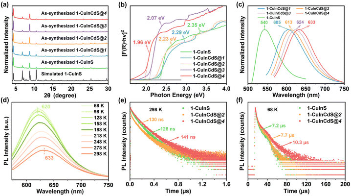
With the influence of trap sites on the Cu-related emission in mind, we attempted to introduce cadmium ions to adjust the wavelength of the Cu related emission. This led to the synthesis of a series of Cd-substituted samples denoted as 1-CuInCdS@n (n = 1–4). It is noted that as n increases, the ratio of Cu to Cd in these as-synthesized samples gradually increases, as illustrated by EDS measurements (Fig. S21 and Table S8†). However, cadmium ions were failed to be introduced in 1-CuGaS and 2-CuGaS, possibly due to the large mismatch of the atomic radius of Ga and Cd ions. PXRD analysis confirmed that 1-CuInCdS@n had the same crystalline configuration with 1-CuInS (Fig. 6a). Furthermore, UV-Vis DRS of 1-CuInCdS@n were also investigated, which indicated that the addition of Cd ions to 1-CuInS indeed led to a decrease in the position of the shallow delocalized trap sites. This decrease became more pronounced with the increase of Cu content in 1-CuInCdS@n (Fig. 6b). Worth of noting is that they all exhibited the same valence band position, as confirmed by UPS (Fig. S14b†). Therefore, the shift of shallow delocalized trap sites was caused by the alteration of the conduction band position. As disclosed in Fig. 6c, 1-CuInCdS@n all exhibited a redshift in PL emission compared to that of 1-CuInS, with emission peaks at 605, 613, 624 and 633 nm, respectively, corresponding to n = 1, 2, 3, and 4. This trend in the PL performance is consistent with the red-shift of the shallow delocalized trap sites. Moreover, the temperature-dependent PLE and PL spectra of 1-CuInCdS@2 and 1-CuInCdS@4 were investigated, which showed a similar blue-shifted tendency as that of 1-CuInS as the temperature decreased (Fig. 6d, S22, S23, and S24†). This phenomenon further illustrated that 1-CuInS and 1-CuInCdS@n had similar luminescence excitation and emission processes. PL decay dynamics of 1-CuInCdS@n were also measured at 298 K (Fig. 6e and S25, and Table S2†) and at 68 K (Fig. 6f and Table S3†). All these data supported that 1-CuInS and 1-CuInCdS@n possess the same decay process. Based on the above results, we can conclude that the introduction of Cd into the framework of 1-CuInS resulted in the redshift of the shallow-delocalized trap sites along with the emission peak.
 |
| | Fig. 6 (a) PXRD of simulated 1-CuInS and as-synthesized 1-CuInS and 1-CuInCdS@n samples. (b) Tauc plots of as-synthesized 1-CuInS and 1-CuInCdS@n. (c) RT PL spectra of as-synthesized 1-CuInS and 1-CuInCdS@n. (d) Temperature-dependent PL spectra of 1-CuInCdS@4. PL decay curve of as-synthesized 1-CuInS and 1-CuInCdS@n with excitation of 390 nm at (e) 298 K and (f) 68 K. | |
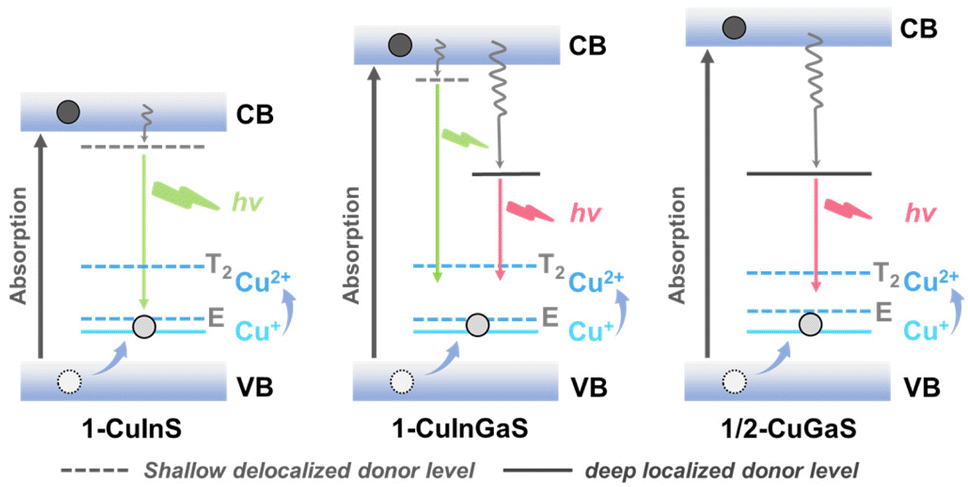
Possible mechanism of exciton recombination
According to the above observations and previous studies, the possible mechanism of exciton recombination is depicted in Scheme 2. After absorption of light, the photo-generated electron and photo-generated hole are distributed in the conduction band (CB) and the valence band (VB), respectively. The process of radiative transition initially involves the capture of a hole from VB to the filled higher potential Cu(I) d-state, forming a transient Cu2+ species that contains a vacancy in the d-shell. The transient Cu2+ state has two different energy states, T2 and E,16,39,42–48 and both can accept an excited electron, which may associated with the broadening of the corresponding emission spectra. Subsequently, the green emission observed in 1-CuInS may be assigned to the recombination of an electron in the shallow-delocalized traps with a hole in the Cu d-state. In the case of 1-CuGaS and 2-CuGaS, the red emission probably attributes to exciton transition from the deep-localized defect state to the Cu d-state, which can be supported by the blueshift of the maximum emission wavelength with the increasing temperature and the relative longer luminescence lifetime. Furthermore, in 1-CuInGaS, both trap sites existed simultaneously, as confirmed by the presence of green and red dual emissions. In addition, when Cd ions were introduced in 1-CuInS, they lead to a downshift of shallow defects due to the reduction of the conduction band energy, resulting in the redshift of the emission peak of 1-CuInCdS@n (Fig. S26†).
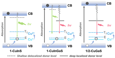 |
| | Scheme 2 Proposed energy level diagram for 1-CuInS, 1-CuInGaS and 1/2-CuGaS. (VB: valence band, CB: conduction band). | |
Conclusion
In summary, we for the first time systematically studied the influence of the composition-determined defect position on the luminescence in the copper-based I–III–VI metal chalcogenide nanoclusters. Three I–III–VI metal chalcogenides (1-CuInS, 1-CuGaS, and 2-CuGaS) with precise structures were selected as unique models to explore the inherent regulation mechanism of the Cu+-related PL emission. Interestingly, 1-CuInS and 1-CuGaS with the same framework structure exhibited a large disparity in PL performance, while 1-CuGaS and 2-CuGaS possessing the same metal components showed similar PL property. Systematic studies shows that the green luminescence of 1-CuInS stemmed from radiative recombination of electrons from shallow-delocalized traps to copper-localized hole and the red emission of 1-CuGaS and 2-CuGaS originated from radiative recombination of electrons from deep localized traps to copper-localized hole. It can conclude that the position of the traps was highly dependent on the surrounding trivalent In3+ and Ga3+ in the clusters, where the presence of In3+ ions will induce the formation of shallow defects and the presence of Ga3+ ions will produce deep defects. The deduction was further confirmed by dual emission properties of the 1-CuInGaS with both In3+ and Ga3+ ions. Moreover, by introducing different contents of Cd ions into the 1-CuInS, we also realized the regulation of luminescence from green emission to red emission. This work sheds light on understanding of the chemical components and defect positions relationship and the mechanism of Cu+-related emission, which will stimulate further regulation of the optoelectronic properties of Cu-based nanoclusters or even nanocrystals and exploration of their potential applications.
Author contributions
Tao Wu and Shang-Fu Yuan: funding acquisition, project administration, resources, writing – reviewing, editing and supervision. Dong-Sheng Li: funding acquisition. Rui Zhou: funding acquisition. Yi-Lei Xu and Yayun Ding: conceptualization, data curation, formal analysis, investigation, methodology, writing – reviewing and editing. Lin-Mei Zhang, Hao Ma, Jia-Xing Liu and Jiaxu Zhang: formal analysis.
Conflicts of interest
There are no conflicts to declare.
Acknowledgements
We acknowledge National Natural Science Foundation of China (22071165, 92261205, 22201103, and U22A20432) and the 111 Project (D20015).
References
- R. Xie, M. Rutherford and X. Peng, Formation of High-Quality I−III−VI Semiconductor Nanocrystals by Tuning Relative Reactivity of Cationic Precursors, J. Am. Chem. Soc., 2009, 131, 5691–5697 CrossRef CAS PubMed.
- H. Zhong, Z. Bai and B. Zou, Tuning the Luminescence Properties of Colloidal I–III–VI Semiconductor Nanocrystals for Optoelectronics and Biotechnology Applications, J. Phys. Chem. Lett., 2012, 3, 3167–3175 CrossRef CAS PubMed.
- C. Guillén, CuInS2 thin films grown sequentially from binary sulfides as compared to layers evaporated directly from the elements, Semicond. Sci. Technol., 2006, 21, 709–712 CrossRef.
- Y.-K. Kim, S.-H. Ahn, K. Chung, Y.-S. Cho and C.-J. Choi, The photoluminescence of CuInS2 nanocrystals: effect of non-stoichiometry and surface modification, J. Mater. Chem., 2011, 22, 1516–1520 RSC.
- H. Nakamura, W. Kato, M. Uehara, K. Nose, T. Omata, S. Otsuka-Yao-Matsuo, M. Miyazaki and H. Maeda, Tunable Photoluminescence Wavelength of Chalcopyrite CuInS2-Based Semiconductor Nanocrystals Synthesized in a Colloidal System, Chem. Mater., 2006, 18, 3330–3335 CrossRef CAS.
- T. Omata, K. Nose and S. Otsuka-Yao-Matsuo, Size dependent optical band gap of ternary I-III-VI2 semiconductor nanocrystals, J. Appl. Phys., 2009, 105, 073106 CrossRef.
- Y.-B. Shan, X.-F. Yue, J.-J. Chen, J.-K. Han, G. Ekoya, L.-G. Hu, R. Liu, Z.-J. Qiu and C.-X. Cong, Revealing layer-dependent interlayer interactions by doping effect on graphene in WSe2/N-layer graphene heterostructures using Raman and photoluminescence spectroscopy, Rare Met., 2022, 41, 3646–3653 CrossRef CAS.
- Z.-W. Zhang, Q.-H. Li, X.-Q. Qiao, D. Hou and D.-S. Li, One-pot hydrothermal synthesis of willow branch-shaped MoS2/CdS heterojunctions for photocatalytic H2 production under visible light irradiation, Chin. J. Catal., 2019, 40, 371–379 CrossRef CAS.
- F.-Y. Tian, D. Hou, F. Tang, M. Deng, X.-q. Qiao, Q. Zhang, T. Wu and D.-S. Li, Novel Zn0.8Cd0.2S@g-C3N4 core–shell heterojunctions with a twin structure for enhanced visible-light-driven photocatalytic hydrogen generation, J. Mater. Chem. A, 2018, 6, 17086–17094 RSC.
- M. Jiao, X. Huang, L. Ma, Y. Li, P. Zhang, X. Wei, L. Jing, X. Luo, A. L. Rogach and M. Gao, Biocompatible off-stoichiometric copper indium sulfide quantum dots with tunable near-infrared emission via aqueous based synthesis, Chem. Commun., 2019, 55, 15053–15056 RSC.
- S. H. Park, A. Hong, J.-H. Kim, H. Yang, K. Lee and H. S. Jang, Highly Bright Yellow-Green-Emitting CuInS2 Colloidal Quantum Dots with Core/Shell/Shell Architecture for White Light-Emitting Diodes, ACS Appl. Mater. Interfaces, 2015, 7, 6764–6771 CrossRef CAS PubMed.
- H. C. Yoon, J. H. Oh, M. Ko, H. Yoo and Y. R. Do, Synthesis and Characterization of Green Zn–Ag–In–S and Red Zn–Cu–In–S Quantum Dots for Ultrahigh Color Quality of Down-Converted White LEDs, ACS Appl. Mater. Interfaces, 2015, 7, 7342–7350 CrossRef CAS PubMed.
- C.-W. Chen, D.-Y. Wu, Y.-C. Chan, C. C. Lin, P.-H. Chung, M. Hsiao and R.-S. Liu, Evaluations of the Chemical Stability and Cytotoxicity of CuInS2 and CuInS2/ZnS Core/Shell Quantum Dots, J. Phys. Chem. C, 2015, 119, 2852–2860 CrossRef CAS.
- W. Guo, X. Sun, O. Jacobson, X. Yan, K. Min, A. Srivatsan, G. Niu, D. O. Kiesewetter, J. Chang and X. Chen, Intrinsically Radioactive [64Cu]CuInS/ZnS Quantum Dots for PET and Optical Imaging: Improved Radiochemical Stability and Controllable Cerenkov Luminescence, ACS Nano, 2015, 9, 488–495 CrossRef CAS PubMed.
- A. C. Berends, F.
T. Rabouw, F. C. M. Spoor, E. Bladt, F. C. Grozema, A. J. Houtepen, L. D. A. Siebbeles and C. de Mello Donegá, Radiative and Nonradiative Recombination in CuInS2 Nanocrystals and CuInS2-Based Core/Shell Nanocrystals, J. Phys. Chem. Lett., 2016, 7, 3503–3509 CrossRef CAS PubMed.
- K. E. Knowles, K. H. Hartstein, T. B. Kilburn, A. Marchioro, H. D. Nelson, P. J. Whitham and D. R. Gamelin, Luminescent Colloidal Semiconductor Nanocrystals Containing Copper: Synthesis, Photophysics, and Applications, Chem. Rev., 2016, 116, 10820–10851 CrossRef CAS PubMed.
- T. Uematsu, T. Doi, T. Torimoto and S. Kuwabata, Preparation of Luminescent AgInS2−AgGaS2 Solid Solution Nanoparticles and Their Optical Properties, J. Phys. Chem. Lett., 2010, 1, 3283–3287 CrossRef CAS.
- M. Uehara, K. Watanabe, Y. Tajiri, H. Nakamura and H. Maeda, Synthesis of CuInS2 fluorescent nanocrystals and enhancement of fluorescence by controlling crystal defect, J. Chem. Phys., 2008, 129, 134709 CrossRef PubMed.
- J. Zhang, P. Feng, X. Bu and T. Wu, Atomically precise metal chalcogenide supertetrahedral clusters: frameworks to molecules, and structure to function, Natl. Sci. Rev., 2021, 9, nwab076 CrossRef PubMed.
- J. Wu, B. Jin, X. Wang, Y. Ding, X.-L. Wang, D. Tang, X. Li, J. Shu, D.-S. Li, Q. Lin, Y.-B. Wu and T. Wu, Breakdown of Valence Shell Electron Pair Repulsion Theory in an H-Bond-Stabilized Linear sp-Hybridized Sulfur, CCS Chem., 2021, 3, 2584–2590 CrossRef CAS.
- J. Zhang, X. Bu, P. Feng and T. Wu, Metal Chalcogenide Supertetrahedral Clusters: Synthetic Control over Assembly, Dispersibility, and Their Functional Applications, Acc. Chem. Res., 2020, 53, 2261–2272 CrossRef CAS PubMed.
- J. Lin, Q. Zhang, L. Wang, X. Liu, W. Yan, T. Wu, X. Bu and P. Feng, Atomically Precise Doping of Monomanganese Ion into Coreless Supertetrahedral Chalcogenide Nanocluster Inducing Unusual Red Shift in Mn2+ Emission, J. Am. Chem. Soc., 2014, 136, 4769–4779 CrossRef CAS PubMed.
- N. Zheng, X. Bu, B. Wang and P. Feng, Microporous and Photoluminescent Chalcogenide Zeolite Analogs, Science, 2002, 298, 2366–2369 CrossRef CAS PubMed.
- J. Lin, L. Wang, Q. Zhang, F. Bu, T. Wu, X. Bu and P. Feng, Highly effective nanosegregation of dual dopants in a micron-sized nanocluster-based semiconductor molecular single crystal for targeting white-light emission, J. Mater. Chem. C, 2016, 4, 1645–1650 RSC.
- H. Yang, J. Zhang, M. Luo, W. Wang, H. Lin, Y. Li, D. Li, P. Feng and T. Wu, The Largest Supertetrahedral Oxychalcogenide Nanocluster and Its Unique Assembly, J. Am. Chem. Soc., 2018, 140, 11189–11192 CrossRef CAS PubMed.
- J. Zhang, C. Qin, Y. Zhong, X. Wang, W. Wang, D. Hu, X. Liu, C. Xue, R. Zhou, L. Shen, Y. Song, D. Xu, Z. Lin, J. Guo, H. Su, D.-S. Li and T. Wu, Atomically precise metal-chalcogenide semiconductor molecular nanoclusters with high dispersibility: Designed synthesis and intracluster photocarrier dynamics, Nano Res., 2020, 13, 2828–2836 CrossRef CAS.
- Y. Hou, T. Wu, L. Wang and P. Feng, Integration of supertetrahedral cluster with reduced graphene oxide sheets for enhanced photostability and photoelectrochemical properties, Sci. China: Chem., 2013, 56, 423–427 CrossRef CAS.
- X. Xu, D. Hu, C. Xue, J. Zhang, D.-S. Li and T. Wu, Exploring the effects of intercluster torsion stress on Mn2+-related red emission from cluster-based layered metal chalcogenides, J. Mater. Chem. C, 2018, 6, 10480–10485 RSC.
- J. Lin, D.-D. Hu, Q. Zhang, D.-S. Li, T. Wu, X. Bu and P. Feng, Improving Photoluminescence Emission Efficiency of Nanocluster-Based Materials by in Situ Doping Synthetic Strategy, J. Mater. Chem. C, 2016, 120, 29390–29396 CAS.
- Y. Liu, J. Zhang, B. Han, X. Wang, Z. Wang, C. Xue, G. Bian, D. Hu, R. Zhou, D.-S. Li, Z. Wang, Z. Ouyang, M. Li and T. Wu, New Insights into Mn–Mn Coupling Interaction-Directed Photoluminescence Quenching Mechanism in Mn2+-Doped Semiconductors, J. Am. Chem. Soc., 2020, 142, 6649–6660 CrossRef CAS PubMed.
- X. Bu, N. Zheng, Y. Li and P. Feng, Pushing Up the Size Limit of Chalcogenide Supertetrahedral Clusters: Two- and Three-Dimensional Photoluminescent Open Frameworks from (Cu5In30S54)13− Clusters, J. Am. Chem. Soc., 2002, 124, 12646–12647 CrossRef CAS PubMed.
- Z.-Q. Li, C.-J. Mo, Y. Guo, N.-N. Xu, Q.-Y. Zhu and J. Dai, Discrete supertetrahedral CuInS nanoclusters and their application in fabrication of cluster-sensitized TiO2 photoelectrodes, J. Mater. Chem. A, 2017, 5, 8519–8525 RSC.
- W.-W. Xiong, J.-R. Li, B. Hu, B. Tan, R.-F. Li and X.-Y. Huang, Largest discrete supertetrahedral clusters synthesized in ionic liquids, Chem. Sci., 2012, 3, 1200–1204 RSC.
- D.-D. Yang, W. Li, W.-W. Xiong, J.-R. Li and X.-Y. Huang, Ionothermal synthesis of discrete supertetrahedral Tn (n = 4, 5) clusters with tunable components, band gaps, and fluorescence properties, Dalton Trans., 2018, 47, 5977–5984 RSC.
- A. A. Bol, J. Ferwerda, J. A. Bergwerff and A. Meijerink, 26-Luminescence of nanocrystalline ZnS:Cu2+, J. Lumin., 2002, 99, 325–334 CrossRef CAS.
- S. M. Thompson, C. Şahin, S. Yang, M. E. Flatté, C. B. Murray, L. C. Bassett and C. R. Kagan, Red Emission from Copper-Vacancy Color Centers in Zinc Sulfide Colloidal Nanocrystals, ACS Nano, 2023, 17, 5963–5973 CrossRef CAS PubMed.
- Y. P. Varshni, Temperature dependence of the energy gap in semiconductors, Physica, 1967, 34, 149–154 CrossRef CAS.
- J. F. Suyver, T. van der Beek, S. F. Wuister, J. J. Kelly and A. Meijerink, Luminescence of nanocrystalline ZnSe:Cu, Appl. Phys. Lett., 2001, 79, 4222–4224 CrossRef CAS.
- P. Peka and H.-J. Schulz, Empirical one-electron model of optical transitions in Cu-doped ZnS and CdS, Phys. B, 1994, 193, 57–65 CrossRef CAS.
- S. Shionoya, T. Koda, K. Era and H. Fujiwara, Nature of Luminescence Transitions in ZnS Crvstals, J. Phys. Soc. Jpn., 1964, 19, 1157–1167 CrossRef CAS.
- P. Mondal and R. Viswanatha, Insights into the Oxidation State of Cu Dopants in II–VI Semiconductor Nanocrystals, J. Phys. Chem. Lett., 2022, 13, 1952–1961 CrossRef CAS PubMed.
- J. L. Birman, Electronic Structure of the Centers in ZnS, Phys. Rev., 1961, 121, 144–145 CrossRef CAS.
- P. Peka and H.-J. Schulz, Unified description of Cu-related luminescence processes in II–VI semiconductors, Solid State Commun., 1994, 89, 225–228 CrossRef CAS.
- S. Gul, J. K. Cooper, C. Corrado, B. Vollbrecht, F. Bridges, J. Guo and J. Z. Zhang, Synthesis, Optical and Structural Properties, and Charge Carrier Dynamics of Cu-Doped ZnSe Nanocrystals, J. Phys. Chem. C, 2011, 115, 20864–20875 CrossRef CAS.
- B. B. Srivastava, S. Jana and N. Pradhan, Doping Cu in Semiconductor Nanocrystals: Some Old and Some New Physical Insights, J. Am. Chem. Soc., 2011, 133, 1007–1015 CrossRef CAS PubMed.
- H. D. Nelson, X. Li and D. R. Gamelin, Computational Studies of the Electronic Structures of Copper-Doped CdSe Nanocrystals: Oxidation States, Jahn–Teller Distortions, Vibronic Bandshapes, and Singlet–Triplet Splittings, J. Phys. Chem. C, 2016, 120, 5714–5723 CrossRef CAS.
- J. K. Cooper, S. Gul, S. A. Lindley, J. Yano and J. Z. Zhang, Tunable Photoluminescent Core/Shell Cu+-Doped ZnSe/ZnS Quantum Dots Codoped with Al3+, Ga3+, or In3+, ACS Appl. Mater. Interfaces, 2015, 7, 10055–10066 CrossRef CAS PubMed.
- S. Gul, J. K. Cooper, P.-A. Glans, J. Guo, V. K. Yachandra, J. Yano and J. Z. Zhang, Effect of Al3+ Co-doping on the Dopant Local Structure, Optical Properties, and Exciton Dynamics in Cu+-Doped ZnSe Nanocrystals, ACS Nano, 2013, 7, 8680–8692 CrossRef CAS PubMed.
Footnotes |
| † Electronic supplementary information (ESI) available: Experimental details, physical measurements, and additional figures and tables. CCDC 2062543 for 1-CuInS, 2062544 for 1-CuGaS and 2062545 for 2-CuGaS. For ESI and crystallographic data in CIF or other electronic format see DOI: https://doi.org/10.1039/d3qi02132g |
| ‡ These authors contributed equally to this work. |
|
| This journal is © the Partner Organisations 2024 |
Click here to see how this site uses Cookies. View our privacy policy here. 
 a,
Hao
Ma
a,
Jia-Xing
Liu
a,
Jiaxu
Zhang
b,
Rui
Zhou
a,
Hao
Ma
a,
Jia-Xing
Liu
a,
Jiaxu
Zhang
b,
Rui
Zhou