
 Open Access Article
 This Open Access Article is licensed under a
 Creative Commons Attribution 3.0 Unported Licence
Prediction and realisation of high mobility and degenerate p-type conductivity in CaCuP thin films†
Joe
Willis
 abc,
Ivona
Bravić
d,
Rekha R.
Schnepf
ef,
Karen N.
Heinselman
e,
Bartomeu
Monserrat
dg,
Thomas
Unold
h,
Andriy
Zakutayev
*e,
David O.
Scanlon
*ab and
Andrea
Crovetto‡
*eh
abc,
Ivona
Bravić
d,
Rekha R.
Schnepf
ef,
Karen N.
Heinselman
e,
Bartomeu
Monserrat
dg,
Thomas
Unold
h,
Andriy
Zakutayev
*e,
David O.
Scanlon
*ab and
Andrea
Crovetto‡
*eh
aDepartment of Chemistry, University College London, 20 Gordon Street, London, WC1H 0AJ, UK. E-mail: d.scanlon@ucl.ac.uk
bThomas Young Centre, University College London, Gower Street, London, WC1E 6BT, UK
cDiamond Light Source Ltd, Harwell Science and Innovation Campus, Didcot, Oxfordshire OX11 0DE, UK
dTheory of Condensed Matter Group, Cavendish Laboratory, University of Cambridge, J. J. Thomson Avenue, Cambridge, CB3 0HE, UK
eNational Renewable Energy Laboratory, Golden, Colorado 80401, USA. E-mail: andriy.zakutayev@nrel.gov; ancro@dtu.dk
fDepartment of Physics, Colorado School of Mines, Golden, Colorado 80401, USA
gDepartment of Materials Science and Metallurgy, University of Cambridge, 27 Charles Babbage Road, Cambridge, CB3 0FS, UK
hDepartment of Structure and Dynamics of Energy Materials, Helmholtz-Zentrum Berlin für Materialien und Energie, GmbH, Berlin, Germany
First published on 26th April 2022
Abstract
Phosphides are interesting candidates for hole transport materials and p-type transparent conducting applications, capable of achieving greater valence band dispersion than their oxide counterparts due to the higher lying energy and increased size of the P 3p orbital. After computational identification of the indirect-gap semiconductor CaCuP as a promising candidate, we now report reactive sputter deposition of phase-pure p-type CaCuP thin films. Their intrinsic hole concentration and hole mobility exceed 1 × 1020 cm−3 and 35 cm2 V−1 s−1 at room temperature, respectively. Transport calculations indicate potential for even higher mobilities. Copper vacancies are identified as the main source of conductivity, displaying markedly different behaviour compared to typical p-type transparent conductors, leading to improved electronic properties. The optical transparency of CaCuP films is lower than expected from first principles calculations of phonon-mediated indirect transitions. This discrepancy could be partly attributed to crystalline imperfections within the films, increasing the strength of indirect transitions. We determine the transparent conductor figure of merit of CaCuP films as a function of composition, revealing links between stoichiometry, crystalline quality, and opto-electronic properties. These findings provide a promising initial assessment of the viability of CaCuP as a p-type transparent contact.
1. Introduction
High performance p-type transparent conducting materials (TCMs) have eluded researchers for decades. As we sit on the cusp of a new era of optoelectronic technologies, such as super high-resolution OLED displays (for which p-type TCMs are preferred over n-type electrodes)1 and even fully transparent display screens and electronics,2 the desire and necessity for reliable p-type TCMs is increasing inexorably. This has led to an explosion in new avenues of p-type TCM research,3–6 with database-screening and machine-learning driven discovery bringing countless potential materials to the attention of the community.7–12 Non-oxides are particularly attractive candidates as p-type TCMs because the valence orbitals on the anion tend to be more diffuse than the oxygen 2p orbitals at the heart of more traditional materials, and often form valence band maxima with greater dispersion. This trend was quantified by Varley and co-workers in 2017, where they surveyed 30000 structures on the Materials Project,13 finding that phosphides had a median hole effective mass around 5me lower than that of oxides.14 This is quite a significant difference, suggesting that phosphides, and indeed other non-oxides, are an exciting class of materials for high hole mobility applications.In addition to good valence band dispersion, an optical band gap exceeding 3.1 eV is required for transparent conductors, corresponding to the shortest wavelength of visible photons. Varley and co-workers also compared the trends in band gap across oxides, sulfides, nitrides and phosphides, finding that the median empirically corrected fundamental density functional theory (DFT) band gap of the phosphides investigated was around 2 eV, roughly half that of the oxides.14 This presents a challenge for phosphides, and in general for non-oxide transparent conductors. However, achieving transparency in materials with a small fundamental band gap is possible. SnO is a bi-polar TCM with an indirect fundamental gap of 0.7 eV, but larger direct gap of 2.7 eV corresponding to the optical transitions, yielding semi-transparency in the visible region.15
Similarly, boron phosphide has an indirect gap of 1.8 eV but a much larger direct optical gap of 4.0 eV.14 The strong overlap of B 2p and P 3p orbitals at the valence band maximum (VBM) yields a hole effective mass of around 0.3me,14 and predicted hole mobility is in excess of 900 cm2 V−1 s−1.16 This exceptional mobility is attributed to the low effective mass and very weak scattering by polar phonons, due to the low ionicity of BP. This is another advantage of non-oxide materials in general for p-type transparent conducting applications – bonding tends to be more covalent, generally leading to a decreased contribution of polar optical phonon scattering to the total scattering process. There are conflicting reports on the optical transparency of BP, as it seems to strongly depend on synthesis conditions, crystallinity, and epitaxial relationships with the substrate.17,18
A current state-of-the-art p-type transparent conducting material (TCM) is copper iodide (CuI), with a figure of merit surpassing that of many oxide based p-type TCMs.19 CuI possesses a direct band gap of around 3.1 eV, and has a doubly degenerate VBM with average hole effective masses of 0.3me and 2.1me for light and heavy holes respectively, indicating relatively good band dispersion.20 The copper vacancy is predicted to be the main source of conductivity under I-rich growth conditions, where it is not charge compensated by native n-type defects.20,21 Room temperature reactive sputter deposition followed by heating in an iodine atmosphere led to a conductivity of 280 S cm−1 while retaining up to 85% optical transmission.19 Thin films of CuI have been trialled successfully as thin film transistors,22 while single crystals of CuI have recently been grown for the first time, capable of acting as a hybrid blue LED.23 The facile deposition, wide direct band gap, self-doping mechanism (under I-rich conditions) and absence of secondary phases make CuI a very attractive p-type transparent conducting non-oxide.
Combining the Cu 3d and P 3p valence orbitals is another viable technique for achieving high valence band dispersion, and was investigated in the ternary phosphides MCuP, where M = Mg, Ca, Ba, and Sr, by Williamson et al. in 2017.24 MgCuP crystallises in the Pnma space group,25 resulting in a Cu atom tetrahedrally coordinated to four P atoms, while CaCuP, BaCuP and SrCuP crystallise in the P63/mmc space group,25,26 where the Cu adopts a trigonal planar configuration with the P atoms forming hexagonal layers of Cu–P sheets (Fig. 1a and b). The trigonal planar coordination of Cu allows for greater spatial overlap and mixing of the Cu 3d states and P 3p states at the valence band maximum compared to tetrahedrally coordinated Cu in MgCuP, at the cost of more anisotropic behaviour. Of the three P63/mmc structures studied computationally, CaCuP emerged as the most promising candidate for p-type TCM applications, and when synthesised as a nominally undoped powder sample it displayed p-type conductivity of around 500 S cm−1 (±50 S cm−1). This is extremely high for a pressed pellet subject to grain boundary and interface scattering. These samples also showed a strong optical absorption onset at around 2.7 eV, in good agreement with predicted behaviour.24 However, the optical absorption coefficient of a powder sample is not easily accessible. These preliminary results justify a more systematic exploration of thin-film CaCuP to investigate potential deposition methods, optical properties, the origin of its electrical conductivity, and the dependence of the latter on growth conditions.
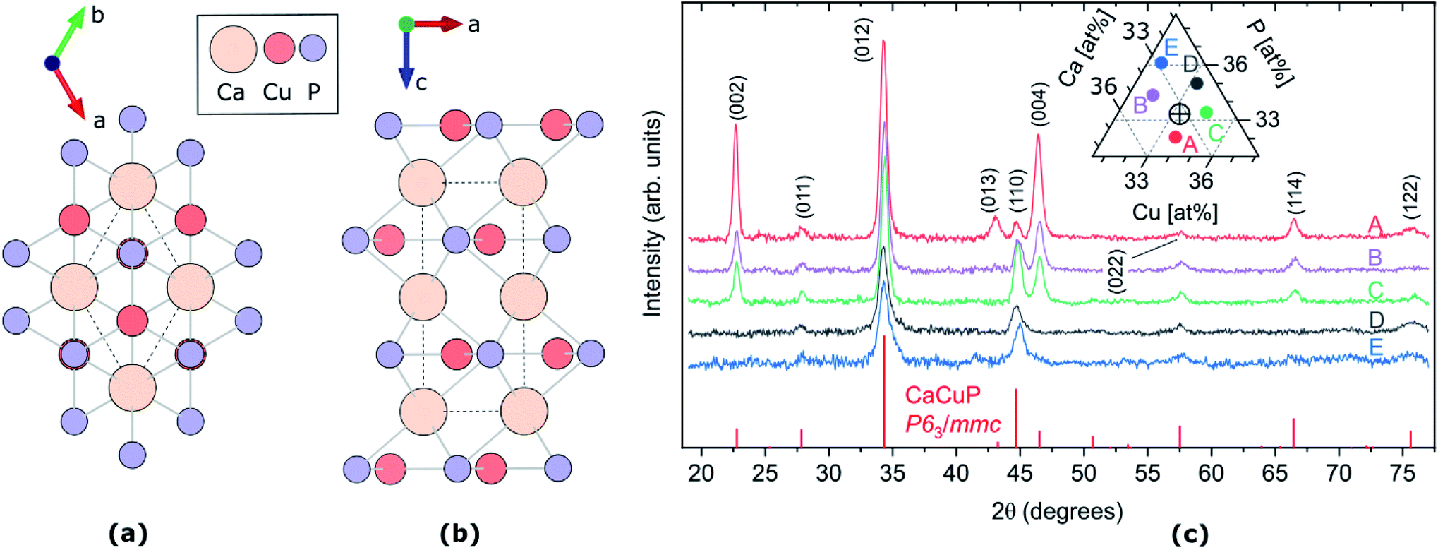 | ||
Fig. 1 (a and b) Crystal structure of CaCuP, space group P63/mmc, along c-axis (a) and b-axis (b). The dotted line represents the primitive unit cell, Ca, Cu and P atoms are represented by pale orange, dark orange and lilac circles, respectively. Visualised using VESTA.27 (c) XRD patterns of five CaCuP films with different compositions around the stoichiometric point (Ca![[thin space (1/6-em)]](https://www.rsc.org/images/entities/char_2009.gif) :Cu:P = 1:1:1). The five compositions are shown in the ternary diagram in the inset, where the stoichiometric point is shown as a cross-hair. The diffraction line intensities expected for randomly oriented CaCuP in the P63/mmc structure26 are shown at the bottom. :Cu:P = 1:1:1). The five compositions are shown in the ternary diagram in the inset, where the stoichiometric point is shown as a cross-hair. The diffraction line intensities expected for randomly oriented CaCuP in the P63/mmc structure26 are shown at the bottom. | ||
In this work, we find that polycrystalline CaCuP thin films with degenerate p-type conductivity and high mobility can be deposited by reactive sputtering. The electrical properties are sensitive to the crystalline quality of the film, which decreases as a function of increasing P content. The optical properties are also sensitive to the crystallinity, with stronger optical absorption recorded in the films of lower crystalline quality. We use density functional theory (DFT) to investigate the defect chemistry of CaCuP, finding the copper vacancy to be extremely low in energy and stable into the valence band maximum, giving rise to degenerate semiconducting behaviour. Charge transport theory is used to model the electrical properties of CaCuP, in reasonable agreement with experimental data, and confirm the trend of improved electrical behaviour with crystal quality. We model the absorption behaviour including phonon-mediated indirect transitions, and find that the experimental absorption coefficient is significantly higher than the theoretical prediction. We calculate the band alignment and TCM figure of merit for CaCuP, and compare these to other p-type transparent conductors.
2. Methodology
2.1. Experimental methods
CaCuP films were deposited on Corning Eagle XG borosilicate glass and crystalline silicon substrates placed in symmetry-equivalent positions with respect to the deposition sources. The deposition technique was reactive radio-frequency (RF) magnetron co-sputtering of metallic Ca and Cu targets in an Ar/PH3 atmosphere. The total sputter pressure and substrate platen temperature were fixed at 5 mTorr and 490 °C respectively in all depositions. Unless otherwise stated, the films presented in this article have thickness between 200 nm and 300 nm. Most characterization was conducted with mapping-type measurements and the resulting combinatorial characterisation data was managed with the custom COMBIgor suite.28 The films on Si were employed for Rutherford backscattering, X-ray fluorescence, and ellipsometry measurements. The films on glass were employed for X-ray diffraction, optical transmission and reflection, and electrical measurements. Consistency between the films grown on the two types of substrates is discussed in the ESI.†X-ray diffraction (XRD) measurements were conducted using Cu Kα radiation and a 2D detector. Elemental composition and film thickness were determined by X-ray fluorescence (XRF) calibrated by Rutherford backscattering spectrometry (RBS) and spectroscopic ellipsometry. Sheet resistance was measured in the substrate plane with a collinear four-point probe. Temperature-dependent Hall carrier concentration and mobility were measured in the substrate plane in the van der Pauw configuration. The absorption coefficient of a stoichiometric film was determined by measuring transmission T at normal incidence and reflection R at near-normal incidence using an integrating sphere to include the diffuse component of both transmission and reflection. The absorption coefficient α was extracted by a standard relationship (see ESI†). The absorption coefficients of a larger number of samples were obtained using only direct transmission and specular reflection (both at normal incidence) measured in a custom-built setup with mapping capabilities. The optical functions of CaCuP (refractive index and extinction coefficient) extending into the UV range were measured by spectroscopic ellipsometry on a thinner film to minimise scattering and depolarisation effects29,30 Further details on the experimental methods can be found in the ESI.†
2.2. Computational methods
First-principles calculations were performed using DFT31,32 within the projector augmented-wave method (PAW)33,34 as implemented in the code VASP.35–38 We used a plane-wave energy cut-off of 400 eV, and a Γ-centred 7 × 7 × 4 k-point mesh to describe the Brillouin zone of the primitive cell. The electrons considered as valence for each element are as follows: Ca 3p64s2 (8 total), Cu 3d104s1 (11 total), P 3s23p3 (5 total). We use the PBEsol functional39 for calculating the vibrational properties and the hybrid PBE0 functional40,41 for all other calculations, in accordance with previous simulations on CaCuP.24 Defect formation energies were calculated according to the Lany–Zunger correction scheme,42–45 thermodynamic stability analysis computed with the CPLAP software,46 charge transport properties calculated using the AMSET code,47 absorption calculations performed using the independent particle approximation (IPA), the electric dipole approximation48 and the Williams–Lax theory,49–51 and the surface band alignment calculations were performed using the SURFAXE code.52 Further details on the computational methods can be found in the ESI.†3. Results and discussion
3.1. Crystal structure and stability
The CaCuP films deposited by reactive sputtering at 490 °C are polycrystalline. In Fig. 1c we show the XRD pattern of five films around the stoichiometric point to illustrate the main trends in their structural properties as a function of the composition. In each film, the diffraction peaks above the noise level can be attributed to CaCuP in the P63/mmc structure.26 Changes in the Cu/Ca ratio do not have a strong influence on the XRD pattern. On the other hand, substantially different patterns are obtained at different P contents (moving vertically in the ternary diagram in the inset of Fig. 1c). When the P content is more than ∼2% above the ideal stoichiometry (Films D and E) the peaks become broader and less intense, indicating a smaller crystallite size and a higher fraction of non-crystalline material in the film, respectively. Furthermore, the (002) and (004) peaks become less intense for increasing P content, compared to the other peaks in the pattern. This indicates a tendency for the c-axis to align closer to the growth direction under P-poor conditions. The grain size of Film C in the substrate plane is on the order of 50 nm as estimated by SEM images (Fig. S9†).We did not observe degradation in CaCuP films in the composition range displayed in Fig. 2 when storing them in a N2-purged box for a few months and occasionally taking them out for measurements under ambient conditions.
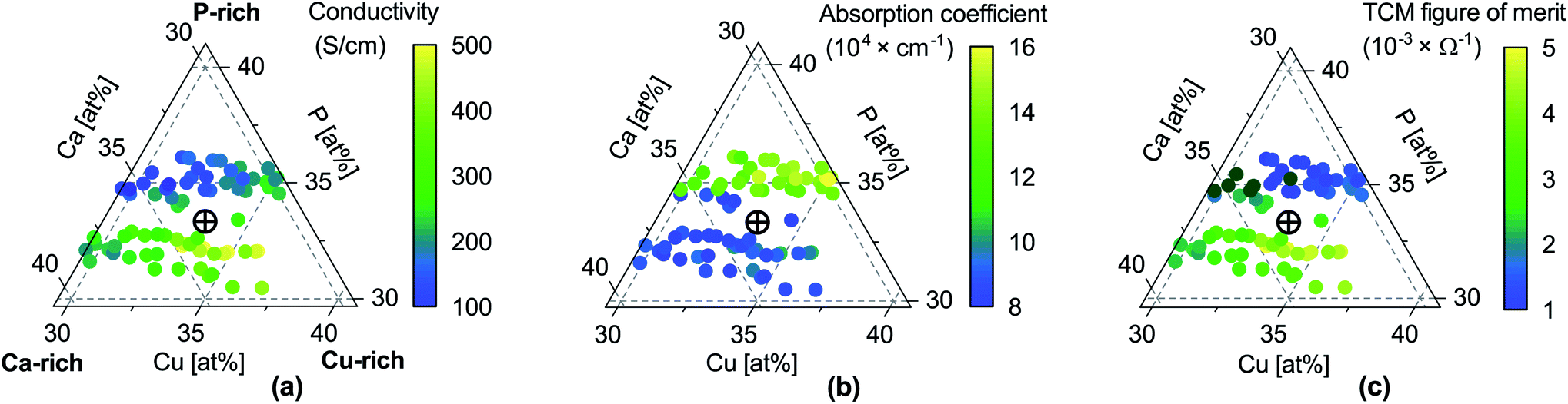 | ||
| Fig. 2 Properties of CaCuP films as a function of composition. (a) Electrical conductivity σ; (b) absorption coefficient α at 550 nm wavelength (centre of the visible region); (c) TCM figure of merit Φ = σ/α, expressing the trade-off between conductivity and transparency following Gordon.53 Unlike the original Gordon figure of merit, we consider α at a single wavelength because the optical transmission of CaCuP films is too low to determine α near the UV edge (see Fig. S14†). In each sub-figure, the cross-hair marks the stoichiometric point (Ca:Cu:P = 1:1:1). | ||
The crystal structure of CaCuP is shown in Fig. 1a and b, and is well reproduced by DFT. It consists of trigonal planar Cu atoms (dark orange) coordinated to P atoms (lilac) in the ab-plane, with Ca atoms (pale orange) sitting above the hexagonal voids in the c-direction. Table S1† shows the lattice parameters obtained after structure optimisation using various exchange–correlation functionals, as well as a comparison to experiment and previous DFT calculations. An extended discussion of the crystal structure–electronic structure relationship in CaCuP can be found in ref. 24. A phonon dispersion curve is produced from lattice-dynamics calculations using a converged 6 × 6 × 6 q-point grid in Fig. S1.† The absence of imaginary phonon modes indicates that CaCuP is dynamically stable.
3.2. Electrical properties
A separate film (Ca:Cu:P = 1.03:1.09:1.00) was deposited in the shape of a Hall cross for further electrical measurements. At room temperature, the (Hall) hole concentration is 1.15 × 1020 cm−3 and the (Hall) hole mobility is 36.4 cm2 V−1 s−1 (Fig. 3). It is interesting to compare these properties to the case of state-of-the-art TCMs without extrinsic doping. Among p-type materials, CuI is one of the compounds with the highest figures of merit. Its highest reported hole concentration and mobility when deposited as a thin film are 1 × 1020 cm−3 and 9 cm2 V−1 s−1 respectively,19 and 1 × 1018 cm−3 and 110 cm2 V−1 s−1 when grown as a single crystal.23 Among the best n-type TCMs with a long research history (In2O3 and ZnO), free electron concentrations in non-epitaxial, intrinsically doped films are generally below 4 × 1020 cm−3 and electron mobilities are below 40 cm2 V−1 s−1.54,55 The electrical properties of p-type CaCuP films are therefore on par with the best n-type intrinsic TCMs.
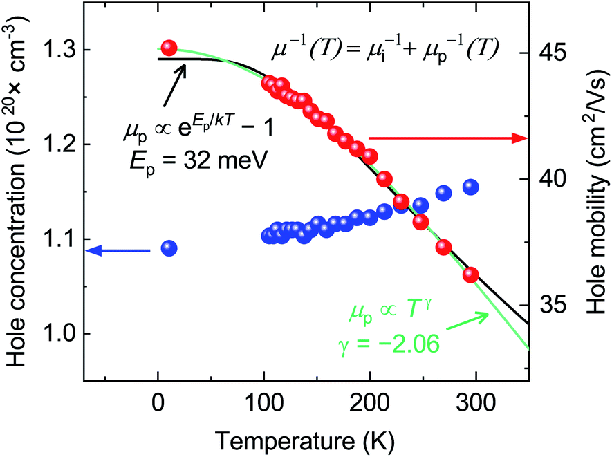 | ||
| Fig. 3 Hall measurements on a near-stoichiometric CaCuP film in the 10 K to 300 K temperature range. Hall hole concentration and mobility plotted in blue and red, respectively. The phonon-limited mobility fit in green is to a generic power law, μp(T) ≡ ATγ, while the fit in black is to the analytically derived expression for optical-phonon limited mobility, μp(T) ≡ B exp(Ep/kBT) − 1. Fits are explained in greater detail in the text. | ||
Knowing the Hall carrier concentration and the Seebeck coefficient (Fig. S11†) we can estimate the effective mass of CaCuP using previously developed theory.56 This analysis yields an effective mass of 0.44 me, in excellent agreement with the direction-averaged heavy hole effective mass (0.43 me) obtained from DFT calculations.24
The hole concentration of CaCuP films rises very slowly with temperature (Fig. 3). This behavior is typical of a degenerately doped semiconductor,57 and is in excellent agreement with defect calculations, which predict degenerate semiconducting behaviour through acceptor levels at or below the valence band maximum, shown in the transition level diagram for the most p-type growth conditions (Fig. 5b). On the other hand, the hole mobility μ(T) decreases with temperature. This trend can be described by considering two parallel scattering channels, so that μ−1(T) = μi−1 + μp−1(T). μi is the mobility resulting from ionised impurity scattering (here, the native acceptors). This term is expected to be nearly temperature-independent for a degenerate semiconductor.58μp(T) ≡ ATγ is a temperature-dependent mobility resulting from phonon scattering. Fitting μi, A and γ to the experimental mobility (shown in green) yields μi = 45.2 cm2 V−1 s−1 and γ = −2.06 (Fig. 3). According to theory developed for p-type III–V semiconductors, γ = −1.5 for purely acoustic phonon scattering and γ < − 1.5 when contributions from optical phonons are also present.59 Similar to CaCuP, III–V semiconductors have a doubly degenerate valence band maximum at the Γ point and typically γ ≃ −2.3.59,60
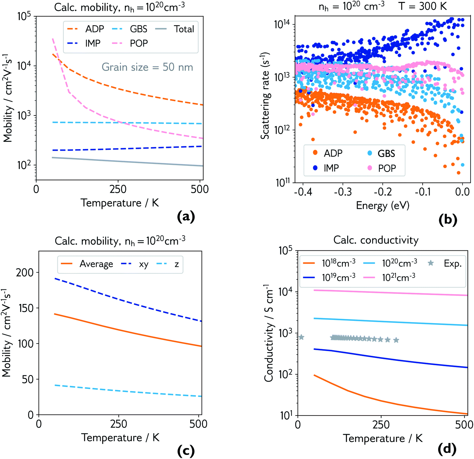 | ||
| Fig. 4 (a) Calculated hole mobility at hole concentration of 1 × 1020 cm−3 and grain size of 50 nm. Mobility is broken down by individual scattering mechanism (ADP = acoustic deformation potential, IMP = ionised impurities, GBS = grain boundary scattering, POP = polar optical phonons), and the total is shown in grey; (b) explicit scattering rates at hole concentration of 1 × 1020 cm−3 and room temperature, for a range of energies below the valence band maximum (0.0 eV), broken down by scattering mechanism; (c) calculated directional hole mobility at hole concentration of 1 × 1020 cm−3; (d) calculated conductivity at various hole concentrations, with experimental conductivity of the film measured in Fig. 3 plotted in grey. | ||
The dominant mobility-limiting mechanism is ionised impurity scattering, showing a very weak temperature dependence. Grain boundary scattering also has a weak temperature dependence but a lower scattering rate, assuming a grain diameter L = 50 nm based on scanning electron microscopy images of the films (Fig. S9†). At around 250 K, polar optical phonon scattering begins to dominate over scattering from grain boundaries, due to its much stronger temperature dependence. Scattering from acoustic phonons has a slightly weaker temperature dependence, and the lowest contribution to the overall scattering rate. The combined effect of these four competing mechanisms is a moderate decrease of the total mobility with temperature, in agreement with experiment. The room-temperature mobility is predicted to be 113 cm2 V−1 s−1, with polar optical phonons becoming increasingly important at high temperatures. These results confirm that it is reasonable to describe the experimental mobility as the reciprocal sum of a temperature independent mobility (representing ionised impurity scattering and potentially grain boundary scattering) and a phonon-limited mobility which is temperature dependent. Since the calculations predict that phonon scattering is predominantly from polar optical phonons, we can replace the generic power law μp(T) ≡ ATγ with the analytically derived expression μp(T) ≡ B exp(Ep/kBT) − 1, where Ep is the energy of the optical phonon mode responsible for hole scattering.60 Fitting again the experimental mobility as μ−1(T) = μi−1 + μp−1(T) with the new expression for μP(T) yields Ep = 32 meV (black line, Fig. 3). This value is in good agreement with the effective optical phonon energy of CaCuP (∼ 27 meV) derived from our calculated phonon band structure following ref. 47 (Fig. S1†).
Fig. 4b shows the explicit scattering rates at energies at and just below the valence band maximum. This confirms that ionised impurity scattering is the predominant scattering mechanism in CaCuP at room temperature. Fig. S6† compares the scattering rates at 1 × 1018 cm−3 and 1 × 1020 cm−3, where a clear switch in the dominant scattering mechanism can be seen – polar optical phonons dominate at lower hole concentrations, and the mobility has a much stronger temperature dependence. Also shown is the effect of decreasing the grain size to 20 nm, which increases the scattering rate from grain boundaries, lowering the total mobility and therefore conductivity, as observed in experiment. We also present directional mobility data in Fig. 4c. Predicted hole mobility is almost four times greater in the xy-direction (in plane) compared to the out of plane (z-direction) mobility. This is as expected, considering the layered structure of CaCuP and the high dispersion that is confined to only two directions in the band structure. This anisotropy may explain why the electrical properties of the films with greater c-axis texturing are superior, when measured in the plane of the substrate.
Finally, the calculated conductivity at various hole concentrations is plotted in Fig. 4d, with experimental conductivity plotted alongside. The change in dominant scattering mechanism from POP to IMP is accompanied by a weaker temperature dependence of the conductivity with increasing hole concentration.
3.3. Defect chemistry
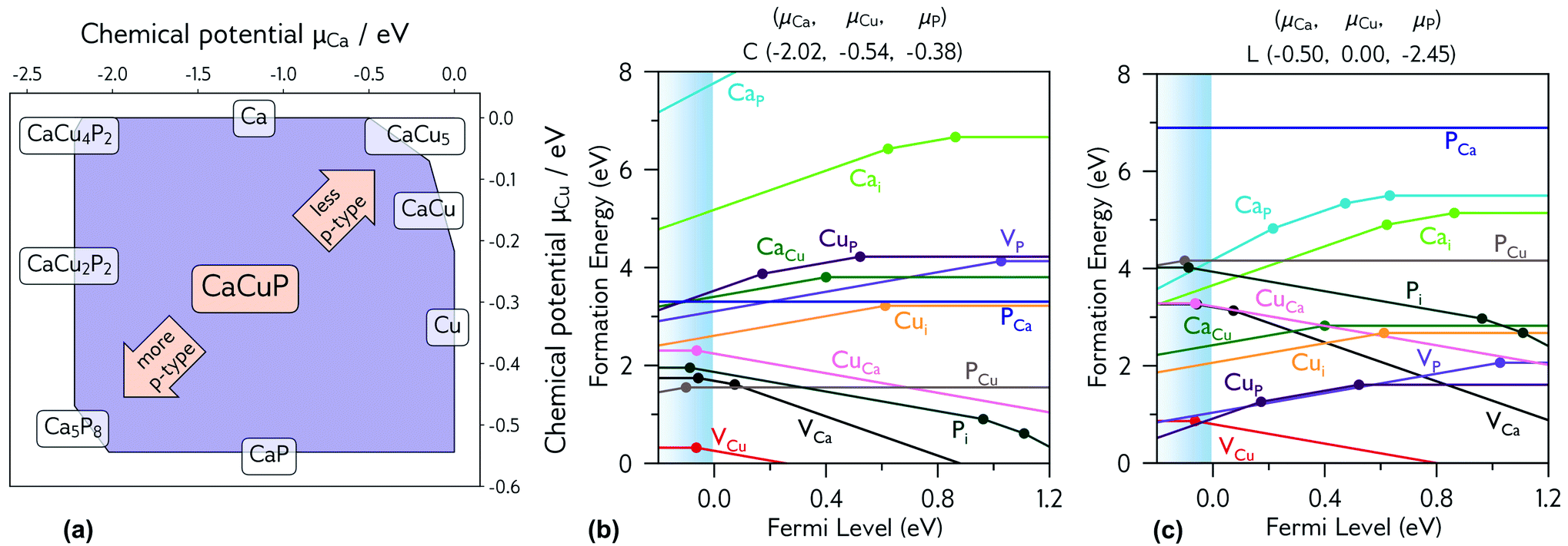 | ||
| Fig. 5 (a) Thermodynamic stability region of CaCuP, calculated using CPLAP;46 (b and c) transition level diagrams for CaCuP calculated under (b) strongly p-type and (c) weakly p-type growth conditions. Plotted using AIDE. Fermi level is plotted on the x-axis against formation energy on the y-axis. The shaded blue region denotes the valence band maximum. Each coloured line denotes a different defect species, and the gradient (positive or negative) denotes the stable charge state at that Fermi level, with horizontal lines denoting neutral charge states. The filled circles denote a thermodynamic transition level (see eqn S(5)†), where two charge states are in equilibrium. | ||
3.3.2. Degenerate defect species
Fig. 5b and c shows the intrinsic defect transition level diagrams for CaCuP under strongly p-type and weakly p-type growth conditions. The lowest energy defect species under the most p-type growth conditions (Fig. 5b) is the copper vacancy (VCu, red), with a formation energy of 0.32 eV when in the neutral charge state. This species is likely to contribute the majority of charge carriers. It is stable in the −1 charge state (when the defect has accepted an electron, generating a hole in the valence band) until around 0.07 eV below the valence band maximum, indicating degenerate behaviour. This is in agreement with the temperature-independent behaviour of the experimentally measured Hall hole concentration. In fact, there are three other degenerate acceptor defects, namely VCa (black), Pi (interstitial, dark cyan), and CuCa (hot pink) which are likely to contribute to p-type conductivity. However, they are not as prevalent as VCu, due to significantly higher formation energies. The PCu defect (grey) does not charge compensate these three species, as it is only stable in the neutral charge state across all Fermi levels. While the best quality CaCuP films are achieved under Ca-poor conditions, it is not the VCa defect that is primarily responsible for p-type conductivity. However, the hole density generated by the Ca vacancy in the −1 charge state is still delocalised throughout the Cu–P network (similar to Cu vacancy hole density in Fig. 6), and the disruption to the crystal structure is spatially separated from the conduction pathway. Similar behaviour is observed in La-doping of the n-type transparent conducting perovskite BaSnO3. The conduction pathways are comprised of SnO6 octahedra, so doping on the Ba site (the A cation site in the ABO3 perovskite structure) does not affect the mobility, and instead drives up conductivity by increasing charge carrier concentration.61–64 This suggests that cation doping on the Ca site could be an effective strategy for increasing the concentration of charge carriers in CaCuP without significant degradation of the mobility.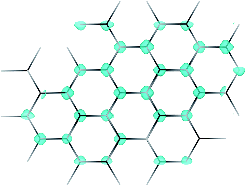 | ||
| Fig. 6 Partial hole density for the copper vacancy in CaCuP. The hole is delocalised throughout the Cu–P plane, in contrast to the largely localised holes that are characteristic of copper vacancies in other p-type transparent conductors. | ||
We can now consider weakly p-type growth conditions, shown in Fig. 5c. Immediately we notice a difference, with the low energy p-type defects from the previous plot moving up in energy, and n-type defects such as the phosphorus vacancy (VP, violet) dropping in energy. However, the lowest energy defect both at the valence band and across all Fermi levels is still VCu, indicating that even under P-poor, metal rich conditions CaCuP is expected to have reasonably good p-type conductivity. Indeed, we see the best conductivity in P-poor films (Fig. 2a).
Clearly the VCu species is the principal defect in CaCuP, and we can now look at it in greater detail. Fig. 6 shows the partial hole density of VCu. The charge density is delocalised throughout the Cu–P layers in the crystal structure, across the same orbitals that comprise the valence band maximum. Therefore, we expect high hole mobility in two directions, as predicted by the charge transport calculations, and as indicated by the highly disperse bands in the Γ → M and Γ → K directions in Fig. S5.† The delocalised nature of this hole is in stark contrast with copper vacancies in p-type transparent conducting oxides. For example, in CuAlO2 the hole generated by VCu is partially localised on the six surrounding Cu atoms, indicative of polaronic behaviour, rather than throughout the whole material.65 Similarly, in Cu2O, the hole density is localised on the four surrounding O atoms.66
3.4. Optical properties
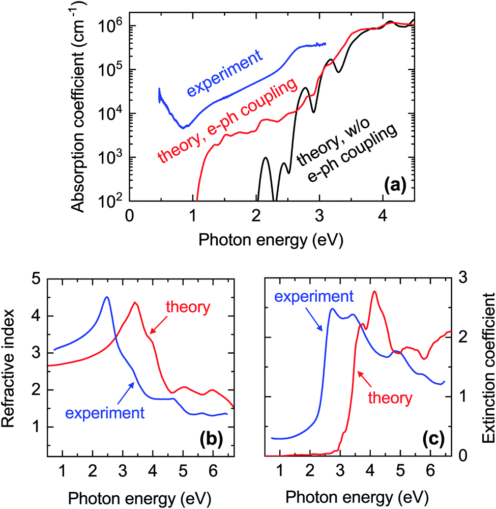 | ||
| Fig. 7 Comparison between experimental and calculated optical properties of CaCuP. (a) Blue line: absorption coefficient extracted from the transmission and reflection measurements (including diffuse components) shown in Fig. S12.† The data is from Film C in Fig. 1. Black line: calculated absorption coefficient with a static lattice and the PBE0 functional (indirect transitions are not included). Red line: calculated absorption coefficient with electron–phonon coupling at 300 K using a 4 × 4 × 4 supercell and the PBE0 functional; (b) refractive index n and (c) extinction coefficient k extended further into the UV. Blue lines: spectra extracted by spectroscopic ellipsometry on a thinner film. Red lines: calculated spectra with electron–phonon coupling. | ||
In Fig. 7a we also show the computed absorption onset at 300 K considering indirect transitions. This simulation includes the effect of electron–phonon coupling, which enables the absorption of a photon across the indirect band gap mediated by the scattering of a phonon. In this case, we see an absorption onset of 1.0 eV, which is significantly closer to the indirect band gap of 1.23 eV at the static lattice value, and in reasonably good agreement with the experimental spectrum. The red-shift of the finite-temperature absorption onset of approximately 200 meV with respect to the static indirect band-gap value can be ascribed to the temperature-dependent renormalisation of the indirect band gap. From this result, we expect the experimental band gap of CaCuP to decrease with increasing temperature as found in most semiconductors. Band gap renormalisations between 50 meV and 200 meV are fairly common when the temperature is elevated from 0 K to 300 K.73–75
To understand these observations, it should be highlighted that the calculated absorption coefficient with electron–phonon coupling assumes a perfectly crystalline material. In a highly disordered material or near grain boundaries, the local lack of crystalline order renders indirect transitions more probable as they can take place without the intervention of a phonon. The grain size of a CaCuP film with stoichiometric P content is only approximately 50 nm (Fig. S9†) and both the crystalline fraction and crystallite size degrade for higher P content. In fact, a strong dependence of optical properties on crystal quality is well known for other indirect band gap materials, such as elemental silicon. Going from fully crystalline to microcrystalline, nanocrystalline and finally fully amorphous Si, the absorption coefficient between the indirect and direct band gap of Si rises accordingly by over an order of magnitude.76 Bulk light scattering effects in the measurement or the approximate treatment of excited states by DFT could also contribute to the experiment-theory discrepancy – the anisotropic nature of CaCuP may result in non-negligible excitonic effects which can increase the absorption coefficient, and are not accounted for in regular DFT. Since experimental absorption exceeds computed absorption over a broad spectral range, it is unlikely that an optically active defect can be responsible for it. Nevertheless, we have calculated the absorption and emission profile of the lowest energy defect, VCu, which can be found in Fig. S7.† As expected, defect absorption and emission are closely spaced in energy and are not expected to cause broadband absorption.
3.5. Band alignment
In Fig. 8 we show the calculated band alignment of CaCuP, and compare this to other popular p-type transparent conductors (left). The calculations predict an electron affinity of 4.0 eV and ionisation potential of 5.2 eV for CaCuP. P-type semiconductors typically have high-lying valence band maxima and conduction band minima, allowing the facile formation of holes while limiting the formation of n-type defects. This is compared to typical n-type materials, which tend to have a much larger electron affinity which drives occupation of the conduction band by electrons.78 The ionisation potential of CaCuP is relatively low, indicating that hole formation is easily achievable – indeed, films of CaCuP display hole (Hall) concentrations on the order of 1 × 1020 cm−3. In fact, the ionisation potential is lower than that of CuI, which suggests that an overall higher concentration of holes could be achieved with an optimised deposition process.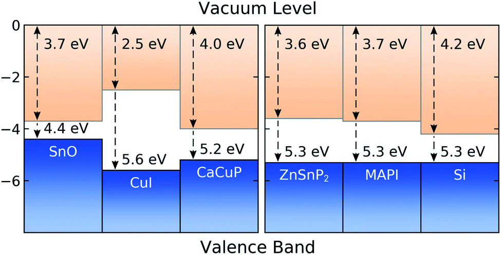 | ||
| Fig. 8 Calculated band alignment of CaCuP, with respect to other state-of-the-art p-type TCMs,15,83 displayed to the left, and to some established and emerging semiconductors (experimentally determined), displayed to the right.80–82 Numbers at the top of the diagram are electron affinities, and those at the bottom are ionisation potentials. Plotted using BAPT. | ||
Ideally, the ionisation potential of a p-type contact material should match the ionisation potential of the semiconductor where holes are to be injected or extracted.79 On the right hand side of Fig. 8, we demonstrate that this is the case for CaCuP when compared against the experimentally determined ionisation potentials for two semiconductors of high technological interest (Si and methylammonium lead iodide, MAPI)80,81 and an emerging phosphide solar absorber (ZnSnP2).82 This indicates that CaCuP could integrate well into various types of devices using these materials. In particular, CaCuP could be a convenient hole transport layer in phosphide-based device stacks.
4. Conclusions
We demonstrated the feasibility of CaCuP thin film growth by reactive sputtering and evaluated its potential as a p-type transparent conductor. The electrical properties of CaCuP films generally confirm the theoretical expectations: CaCuP is a degenerate p-type semiconductor with a high hole mobility, even in non-epitaxial, polycrystalline films. The Cu–P hexagonal sheets throughout the crystal structure enable delocalisation of the hole generated by low energy copper vacancies, leading to large hole mobility in two directions. Ionised impurity scattering is predicted to be the dominant scattering mechanism at the carrier concentrations achieved experimentally in this study (1 × 1020 cm−3), and the experimental temperature dependence of the mobility is qualitatively reproduced by the calculations. P content in the films was found to have a strong influence on crystal quality, which in turn determined the opto-electronic properties. Lower crystallinity is correlated with lower electrical conductivity, and also with higher absorption coefficients in the spectral region where indirect transitions dominate. Regardless of film composition, the absorption coefficient of CaCuP films was unexpectedly high. Hence, the maximum figure of merit of CaCuP as a transparent conductor was substantially lower than in the best n-type TCMs and somewhat lower than the highest values achieved by the state-of-the-art p-type TCM CuI.Nevertheless, band alignment calculations show that the ionisation potential of CaCuP matches the valence band position of various semiconductors of technological interest. Thus, it may be possible to integrate CaCuP as a contact layer into device structures where full transparency is not required. We call on the community for further experimental investigation of CaCuP with focus on its optical properties. Growth of high-quality single crystals would be particularly useful to investigate if the high absorption coefficient of the present CaCuP samples is an intrinsic feature of the material or the consequence of a less-than-ideal growth process. Beyond-DFT calculations that provide an improved description of the band gap (GW theory) and excited states (Bethe–Salpeter formalism) would also provide a clearer picture of the optical properties of CaCuP. Finally, exploration of other thin-film synthesis routes, epitaxial growth, and extrinsic doping would help to build a more robust assessment of CaCuP as a transparent conductor and opto-electronic material in general.
Author contributions
JW conceptualised and prepared the manuscript, with major contributions from IB and AC, under the guidance of DOS. AC conceptualised and implemented the experimental work, including thin film deposition, most characterisation, and experimental data analysis. Computational work and analysis was performed by JW and IB under the guidance of DOS and BM. RRS and AZ designed and set up the reactive sputtering system. KNH conducted RBS measurements and analysis. Experimental findings were often discussed between AC, TU and AZ. All authors provided input to the manuscript.Conflicts of interest
There are no conflicts to declare.Data availability
The experimental and computational data shown in this article is available at the following DOI: https://doi.org/10.5281/zenodo.6281750. Additional experimental data is available at the following URL: https://htem.nrel.gov/ (doi: https://doi.org/10.7799/1407128).Acknowledgements
This project has received funding from the European Union’s Horizon 2020 research and innovation programme under the Marie Sklodowska-Curie grant agreement no. 840751 (synthesis, characterization, and experimental data analysis work). This work was authored in part at the National Renewable Energy Laboratory, operated by Alliance for Sustainable Energy, LLC, for the U.S. Department of Energy (DOE) under contract no. DE-AC36-08GO28308. The views expressed in this article do not necessarily represent the views of the DOE or the US government. Funding supporting development and operation of synthesis and characterization equipment (RRS, KNH, AZ) was provided by the Office of Science, Office of Basic Energy Sciences. JW and DOS acknowledge Diamond Light Source Ltd for co-sponsorship of an EngD studentship on the EPSRC Centre for Doctoral Training in Molecular Modelling and Materials Science (EP/L015862/1). This work used the ARCHER and ARCHER2 UK National Supercomputing Service (https://www.archer2.ac.uk), via our membership of the UK's HEC Materials Chemistry Consortium, which is funded by the EPSRC (EP/L000202, EP/R029431 and EP/T022213), and the UK Materials and Molecular Modelling (MMM) Hub (Thomas EP/P020194 and Young EP/T022213). The UCL Grace, Kathleen and Thomas HPC Facilities (Grace@UCL, Kathleen@UCL, Thomas@UCL) were also used in the completion of this work. JW thanks Dr Anna Regoutz and Dr Benjamin A. D. Williamson for insightful discussions about this project. AC thanks Dr Sage Bauers for assistance with electrical measurements. IB and BM acknowledge support from the Winton Programme for Physics of Sustainability. BM also acknowledges support from a UKRI Future Leaders Fellowship (grant no. MR/V023926/1) and from the Gianna Angelopoulos Programme for Science, Technology and Innovation. This work made use of resources provided by the Cambridge Tier-2 system, operated by the University of Cambridge Research Computing Service (https://www.hpc.cam.ac.uk) and funded by Tier-2 capital grant EP/P020258/1.Notes and references
- J. F. Wager, Inf. Disp., 2014, 30, 26–29 Search PubMed.
- Transparent Electronics Market – Growth, Trends and Forecast (2020–2025), 2020, https://www.mordorintelligence.com/industry-reports/transparent-electronics-market Search PubMed.
- J. Willis and D. O. Scanlon, J. Mater. Chem. C, 2021, 9, 11995–12009 RSC.
- L. Hu, R. H. Wei, X. W. Tang, W. J. Lu, X. B. Zhu and Y. P. Sun, J. Appl. Phys., 2020, 128, 140902 CrossRef CAS.
- Z. Wang, P. K. Nayak, J. A. Caraveo-Frescas and H. N. Alshareef, Adv. Mater., 2016, 28, 3831–3892 CrossRef CAS PubMed.
- K. H. L. Zhang, K. Xi, M. G. Blamire and R. G. Egdell, J. Phys.: Condens. Matter, 2016, 28, 383002 CrossRef PubMed.
- D. Dahliah, G. Brunin, J. George, V.-A. Ha, G.-M. Rignanese and G. Hautier, Energy Environ. Sci., 2021, 14, 5057–5073 RSC.
- D. Dahliah, G.-M. Rignanese and G. Hautier, J. Mater. Chem. C, 2020, 8, 9352–9357 RSC.
- S. Hu, B. Xia, Y.-P. Lin, T. Katase, J. Fujioka, T. Kamiya, H. Hosono, K.-Z. Du and Z. Xiao, Adv. Funct. Mater., 2020, 30, 1909906 CrossRef CAS.
- B. A. D. Williamson, G. J. Limburn, G. W. Watson, G. Hyett and D. O. Scanlon, Matter, 2020, 3, 759–781 CrossRef PubMed.
- G. Brunin, F. Ricci, V.-A. Ha, G.-M. Rignanese and G. Hautier, npj Comput. Mater., 2019, 5, 63 CrossRef.
- D. W. Davies, K. T. Butler and A. Walsh, Chem. Mater., 2019, 31, 7221–7230 CrossRef CAS.
- A. Jain, S. P. Ong, G. Hautier, W. Chen, W. D. Richards, S. Dacek, S. Cholia, D. Gunter, D. Skinner, G. Ceder and K. A. Persson, APL Mater., 2013, 1, 011002 CrossRef.
- J. B. Varley, A. Miglio, V.-A. Ha, M. J. van Setten, G.-M. Rignanese and G. Hautier, Chem. Mater., 2017, 29, 2568–2573 CrossRef CAS.
- N. F. Quackenbush, J. P. Allen, D. O. Scanlon, S. Sallis, J. A. Hewlett, A. S. Nandur, B. Chen, K. E. Smith, C. Weiland, D. A. Fischer, J. C. Woicik, B. E. White, G. W. Watson and L. F. J. Piper, Chem. Mater., 2013, 25, 3114–3123 CrossRef CAS.
- V.-A. Ha, B. Karasulu, R. Maezono, G. Brunin, J. B. Varley, G.-M. Rignanese, B. Monserrat and G. Hautier, Phys. Rev. Mater., 2020, 4, 065401 CrossRef CAS.
- A. Crovetto, J. M. Adamczyk, R. R. Schnepf, C. L. Perkins, H. Hempel, S. R. Bauers, E. S. Toberer, A. C. Tamboli, T. Unold and A. Zakutayev, Adv. Mater. Interfaces, 2022, 2200031 CrossRef CAS.
- M. Odawara, T. Udagawa and G. Shimaoka, Jpn. J. Appl. Phys., 2005, 44, 681–683 CrossRef CAS.
- C. Yang, M. Kneiβ, M. Lorenz and M. Grundmann, Proc. Natl. Acad. Sci. U. S. A., 2016, 113, 12929–12933 CrossRef CAS PubMed.
- J. Wang, J. Li and S.-S. Li, J. Appl. Phys., 2011, 110, 054907 CrossRef.
- H. Chen, C.-Y. Wang, J.-T. Wang, Y. Wu and S.-X. Zhou, Phys. B, 2013, 413, 116–119 CrossRef CAS.
- A. Liu, H. Zhu, W.-T. Park, S.-J. Kang, Y. Xu, M.-G. Kim and Y.-Y. Noh, Adv. Mater., 2018, 30, 1802379 CrossRef PubMed.
- D. Ahn, J. D. Song, S. S. Kang, J. Y. Lim, S. H. Yang, S. Ko, S. H. Park, S. J. Park, D. S. Kim, H. J. Chang and J. Chang, Sci. Rep., 2020, 10, 3995 CrossRef CAS PubMed.
- B. A. D. Williamson, J. Buckeridge, J. Brown, S. Ansbro, R. G. Palgrave and D. O. Scanlon, Chem. Mater., 2017, 29, 2402–2413 CrossRef CAS.
- A. Mewis, Z. Naturforsch. B, 1979, 34, 1373–1376 CrossRef.
- A. Mewis, Z. Naturforsch. B, 1978, 33, 983–986 CrossRef.
- K. Momma and F. Izumi, J. Appl. Crystallogr., 2008, 41, 653–658 CrossRef CAS.
- K. R. Talley, S. R. Bauers, C. L. Melamed, M. C. Papac, K. N. Heinselman, I. Khan, D. M. Roberts, V. Jacobson, A. Mis, G. L. Brennecka, J. D. Perkins and A. Zakutayev, ACS Comb. Sci., 2019, 21, 537–547 CrossRef CAS PubMed.
- A. Crovetto, A. Cazzaniga, R. B. Ettlinger, J. Schou and O. Hansen, Thin Solid Films, 2015, 582, 203–207 CrossRef CAS.
- A. Crovetto, A. Cazzaniga, R. B. Ettlinger, J. Schou and O. Hansen, Sol. Energy Mater. Sol. Cells, 2018, 187, 233–240 CrossRef CAS.
- P. Hohenberg and W. Kohn, Phys. Rev., 1964, 136, 864–871 CrossRef.
- W. Kohn and L. J. Sham, Phys. Rev., 1965, 140, 1131 CrossRef.
- P. E. Blöchl, Phys. Rev. B: Condens. Matter Mater. Phys., 1994, 50, 7953 CrossRef PubMed.
- G. Kresse and D. Joubert, Phys. Rev. B: Condens. Matter Mater. Phys., 1999, 59, 1758–1775 CrossRef CAS.
- G. Kresse and J. Furthmüller, Phys. Rev. B: Condens. Matter Mater. Phys., 1996, 54, 11169–11186 CrossRef CAS PubMed.
- G. Kresse and J. Furthmüller, Comput. Mater. Sci., 1996, 6, 15–50 CrossRef CAS.
- G. Kresse and J. Hafner, Phys. Rev. B: Condens. Matter Mater. Phys., 1994, 49, 14251–14269 CrossRef CAS PubMed.
- G. Kresse and J. Hafner, Phys. Rev. B: Condens. Matter Mater. Phys., 1993, 47, 558–561 CrossRef CAS PubMed.
- J. P. Perdew, A. Ruzsinszky, G. I. Csonka, O. A. Vydrov, G. E. Scuseria, L. A. Constantin, X. Zhou and K. Burke, Phys. Rev. Lett., 2008, 100, 136406 CrossRef PubMed.
- C. Adamo and V. Barone, J. Chem. Phys., 1999, 110, 6158–6170 CrossRef CAS.
- J. Paier, R. Hirschl, M. Marsman and G. Kresse, J. Chem. Phys., 2005, 122, 234102 CrossRef PubMed.
- S. Lany and A. Zunger, Phys. Rev. B: Condens. Matter Mater. Phys., 2008, 78, 235104 CrossRef.
- S. Lany and A. Zunger, Modell. Simul. Mater. Sci. Eng., 2009, 17, 084002 CrossRef.
- G. Makov and M. C. Payne, Phys. Rev. B: Condens. Matter Mater. Phys., 1995, 51, 4014–4022 CrossRef CAS PubMed.
- S. T. Murphy and N. D. M. Hine, Phys. Rev. B: Condens. Matter Mater. Phys., 2013, 87, 094111 CrossRef.
- J. Buckeridge, D. Scanlon, A. Walsh and C. Catlow, Comput. Phys. Commun., 2014, 185, 330–338 CrossRef CAS.
- A. M. Ganose, J. Park, A. Faghaninia, R. Woods-Robinson, K. A. Persson and A. Jain, Nat. Commun., 2021, 12, 2222 CrossRef CAS PubMed.
- M. Gajdoš, K. Hummer, G. Kresse, J. Furthmüller and F. Bechstedt, Phys. Rev. B: Condens. Matter Mater. Phys., 2006, 73, 045112 CrossRef.
- F. Williams, Phys. Rev., 1951, 82, 281–282 CrossRef CAS.
- M. Lax, J. Chem. Phys., 1952, 20, 1752–1760 CrossRef CAS.
- B. Monserrat, Phys. Rev. B, 2016, 93, 014302 CrossRef.
- K. Brlec, D. W. Davies and D. O. Scanlon, J. Open Source Softw., 2021, 6, 3171 CrossRef.
- R. G. Gordon, MRS Bull., 2000, 25, 52–57 CrossRef CAS.
- M. Hála, S. Fujii, A. Redinger, Y. Inoue, G. Rey, M. Thevenin, V. Deprédurand, T. P. Weiss, T. Bertram and S. Siebentritt, Prog. Photovoltaics Res. Appl., 2015, 23, 1630–1641 CrossRef.
- K. Utsumi, H. Iigusa, R. Tokumaru, P. Song and Y. Shigesato, Thin Solid Films, 2003, 445, 229–234 CrossRef CAS.
- G. J. Snyder, A. Pereyra and R. Gurunathan, Adv. Funct. Mater., 2022, 2112772 CrossRef.
- K. Ellmer and R. Mientus, Thin Solid Films, 2008, 516, 4620–4627 CrossRef CAS.
- R. Dingle, Philos. Mag., 1955, 46, 831–840 CAS.
- J. D. Wiley and M. DiDomenico, Phys. Rev. B: Solid State, 1970, 2, 427–433 CrossRef.
- W. A. Harrison, Phys. Rev., 1956, 104, 1281–1290 CrossRef CAS.
- H. J. Kim, U. Kim, H. M. Kim, T. H. Kim, H. S. Mun, B.-G. Jeon, K. T. Hong, W.-J. Lee, C. Ju, K. H. Kim and K. Char, Appl. Phys. Express, 2012, 5, 061102 CrossRef.
- D. O. Scanlon, Phys. Rev. B: Condens. Matter Mater. Phys., 2013, 87, 161201 CrossRef.
- Z. Lebens-Higgins, D. Scanlon, H. Paik, S. Sallis, Y. Nie, M. Uchida, N. Quackenbush, M. Wahila, G. Sterbinsky, D. A. Arena, J. Woicik, D. Schlom and L. Piper, Phys. Rev. Lett., 2016, 116, 027602 CrossRef CAS PubMed.
- C. W. Myung, G. Lee and K. S. Kim, J. Mater. Chem. A, 2018, 6, 23071–23077 RSC.
- D. O. Scanlon and G. W. Watson, J. Phys. Chem. Lett., 2010, 1, 3195–3199 CrossRef CAS.
- D. O. Scanlon, B. J. Morgan, G. W. Watson and A. Walsh, Phys. Rev. Lett., 2009, 103, 096405 CrossRef PubMed.
- R. D. Shannon, Acta Crystallogr., Sect. A, 1976, 32, 751–767 CrossRef.
- A. Janotti and C. G. V. de Walle, Phys. Rev. B: Condens. Matter Mater. Phys., 2007, 76, 165202 CrossRef.
- D. O. Scanlon and G. W. Watson, J. Mater. Chem., 2012, 22, 25236 RSC.
- P. R. L. Keating, D. O. Scanlon, B. J. Morgan, N. M. Galea and G. W. Watson, J. Phys. Chem. C, 2012, 116, 2443–2452 CrossRef CAS.
- D. O. Scanlon, A. B. Kehoe, G. W. Watson, M. O. Jones, W. I. F. David, D. J. Payne, R. G. Egdell, P. P. Edwards and A. Walsh, Phys. Rev. Lett., 2011, 107, 246402 CrossRef PubMed.
- M. Burbano, D. O. Scanlon and G. W. Watson, J. Am. Chem. Soc., 2011, 133, 15065–15072 CrossRef CAS PubMed.
- W. M. Linhart, S. J. Zelewski, P. Scharoch, F. Dybała and R. Kudrawiec, J. Mater. Chem. C, 2021, 9, 13733–13738 RSC.
- B. Monserrat, C. E. Dreyer and K. M. Rabe, Phys. Rev. B, 2018, 97, 104310 CrossRef CAS.
- F. Giustino, Rev. Mod. Phys., 2017, 89, 015003 CrossRef.
- G. E. Jellison, M. F. Chisholm and S. M. Gorbatkin, Appl. Phys. Lett., 1993, 62, 3348–3350 CrossRef CAS.
- A. Crovetto, H. Hempel, M. Rusu, L. Choubrac, D. Kojda, K. Habicht and T. Unold, ACS Appl. Mater. Interfaces, 2020, 12, 48741–48747 CrossRef CAS PubMed.
- M. Einhorn, B. A. D. Williamson and D. O. Scanlon, J. Mater. Chem. A, 2020, 8, 7914–7924 RSC.
- A. M. Ganose, C. N. Savory and D. O. Scanlon, J. Mater. Chem. A, 2017, 5, 7845–7853 RSC.
- J. R. Harwell, T. K. Baikie, I. D. Baikie, J. L. Payne, C. Ni, J. T. S. Irvine, G. A. Turnbull and I. D. W. Samuel, Phys. Chem. Chem. Phys., 2016, 18, 19738–19745 RSC.
- W. Monch, Semiconductor Surfaces and Interfaces, Springer, Berlin, 3rd edn, 2001 Search PubMed.
- T. Kuwano, R. Katsube, K. Kazumi and Y. Nose, Sol. Energy Mater. Sol. Cells, 2021, 221, 110891 CrossRef CAS.
- J. H. Lee, B. H. Lee, J. Kang, M. Diware, K. Jeon, C. Jeong, S. Y. Lee and K. H. Kim, Nanomaterials, 2021, 11, 1237 CrossRef PubMed.
Footnotes |
| † Electronic supplementary information (ESI) available. See https://doi.org/10.1039/d2sc01538b |
| ‡ Current address: DTU Nanolab, Technical University of Denmark, Ørsteds Plads, 2800 Kgs, Lyngby, Denmark |
| This journal is © The Royal Society of Chemistry 2022 |