Universal selection rule for surfactants used in miniemulsion processes for eco-friendly and high performance polymer semiconductors†
Received
13th July 2017
, Accepted 31st August 2017
First published on 31st August 2017
Abstract
Commercial interest in the environmentally friendly processing of polymer semiconductors is on the rise. To reduce noxious solvent use and to realize water-borne colloids of polymer semiconductors, we developed a universal and eco-friendly miniemulsion process to satisfy four essential criteria: (1) efficient emulsification for synthesizing small and uniform polymer semiconductor particles, (2) efficient coalescence of particles to yield high quality thin films with low roughness and high fill-factors, (3) efficient removal of residual surfactants, and (4) high ordering of polymers within particles. We screened various surfactants to find conditions that satisfied the suggested selection rules regardless of the charge polarity and molecular structure of the polymer semiconductor. Our universal method can be applied to first-generation polythiophene derivatives as well as to the latest p-type, n-type and ambipolar polymers with planar backbones and high charge carrier mobility. Using these results, we fabricated for the first time a high-performance complementary inverter and a photodiode using water as a processing solvent.
Broader context
Organic semiconductors are key building blocks for future electronic and energy devices that require unprecedented properties such as low-weight, flexibility, and portability. Although the issues related to the low charge-carrier mobility of organic semiconductors have been greatly overcome by novel molecular design & synthesis, undesirable processing conditions still limit their commercial application. Up to now, all the high performance organic semiconductors reported in the literature have been processed from toxic solvents such as chloroform, chlorobenzene or other organic solvents. In this work, we propose a universal colloid technique that can successfully produce water-borne semiconductor inks, which can be applied to all high-performance p-type, n-type and ambipolar polymer semiconductors. Systematic experiments and analyses were carefully conducted for 18 surfactants under the strategically determined objects of fine film morphology, surfactant elimination and high charge carrier mobility. As a result, we could develop a universal colloid technique which satisfies all the criteria and thus gives high opto-electronic performances of water-borne polymer semiconductors. This universal colloid technique enables the environmentally friendly manufacture of a wide variety of polymer-based electronic and energy devices, which can contribute significantly to the commercial applications of polymeric semiconductor materials.
|
Introduction
Polymer semiconductors have shown potential to pave the way for a new generation of electronic devices, owing to their unique characteristics such as low weight, compatibility with a flexible substrate, and the possibility of low cost/low temperature solution processing.1–3 Furthermore, when applied to energy devices, polymer semiconductors enable rapid energy payback time due to the long-term sustainability of organics compared to silicon and other photovoltaic technologies.4 Specifically, donor–acceptor polymers with rigid/planar backbone molecular structures, which can increase tolerance to the inevitable large amounts of disorder in polymer aggregates, have exhibited unprecedented high hole and electron mobilities exceeding 8 cm2 V−1 s−1.5–7
Unfortunately, these polymer semiconductors are mostly processed via solution processes employing toxic solvents such as chloroform and chlorobenzene, which can have serious adverse effects on the environment and human health.8 Considering the environmental regulations of governments, which continue to be strengthened, solution processing based on such toxic solvents is unsustainable in terms of commercial applications of polymer semiconductors. Therefore, over the past several years, research on processing polymer semiconductors in a more environmentally friendly manner has been conducted. These efforts can be roughly classified into three methods: (1) introducing hydrophilic functional groups into the side chains of polymer semiconductors so that they can be directly dissolved in an environmentally friendly solvent such as water and (2) introducing surfactant-free colloid techniques and (3) introducing surfactant-containing colloid techniques to polymer semiconductors so that they can be dispersed in an environmentally friendly solvent as a colloid. The first method is represented by research efforts geared towards synthesizing water-soluble polymer semiconductors. For instance, Shao et al. reported the synthesis of a thiophene-based conjugated polymer with triethylene glycol side chains which can be successfully dissolved in water with reasonably high solubility.9 They demonstrated polymer field effect transistors (PFETs) with a relatively low charge carrier mobility value of 10−3 cm2 V−1 s−1. After this finding, many similar studies were conducted, however, it is hard to find a case where the charge mobility of the water-processed PFET was improved to a meaningful level. This is presumably due to the lack of efficient lamellar structuring of polymer chains caused by repulsion between polar side chains or charge trapping effects caused by strong local charges of functional side chains. The second method has been widely reported by many researchers in organic electronics because high electrical performances could be realized due to the absence of the electrically inert additives such as surfactants.10–13 Gärtner et al. reported OPVs fabricated from a surfactant-free, alcohol-based colloid with a PCE of 4.1%.10 More recently, a method for long-lived suspensions of polymer semiconductors in water without surfactants has been systematically studied.11 However, we want to address that this method is difficult to be applied to new generation polymer semiconductors with highly planar backbone structures and thus highly aggregating nature. The third method was initiated by Landfester et al., who proposed a miniemulsion process of polymer semiconductors by using sodium dodecyl sulfate (SDS) as a surfactant, resulting in well-dispersed, water-borne colloidal solutions.14 This method can be more beneficial than the previous methods because stable colloids with small-sized nanoparticles can be guaranteed which can induce high quality thin films. At the same time, there is a problem as abundant amounts of surfactant molecules may remain after fabricating the thin films, which can seriously interfere with charge transport.15 Therefore, extensive research on the effective removal of residual surfactants has been carried out. Ethirajan et al. reported high-performance water-borne OPVs with a power conversion efficiency (PCE) of 3.8% using a polymer semiconductor as a donor. In this report, they tried to eliminate surfactant molecules with more than 12 h of dialysis.16 Our group reported a water-borne colloid technique using a non-ionic surfactant with an unprecedentedly high charge-carrier mobility of 2.5 cm2 V−1 s−1.17 In this case, non-ionic surfactants could be easily eliminated via a post-washing process due to the low efficiency of their adsorption on the polymer surface. Although these studies have shown some promise in the removal of surfactants, considering the ever-evolving complex backbone structure of polymer semiconductors and especially n-type polymer semiconductors that have not yet successfully been dispersed as an aqueous colloid, a colloid technique that can be applied more universally and regardless of polarity is urgently needed.
In this study, we propose a universal colloid technique that can successfully produce water-based semiconductor thin films from all high-performance p-type, n-type and ambipolar polymer semiconductors. Systematic experiments and analyses were carefully conducted for 18 surfactants in order to obtain fine film morphology, surfactant elimination and high charge carrier mobility. We first applied a mini-emulsion colloidization technique using various surfactants to naphthalene tetracarboxydiimide-based (NDI) n-type polymer semiconductors with highly planar backbones and high charge mobility to find a universal surfactant satisfying the above four targets.18 We demonstrate that the selected surfactant can be applied not only to NDI-based n-type polymers but also to various high-performance polymer semiconductor materials, enabling the fabrication of a high performance complementary inverter as well as a high detectivity multi-layer stacked photodiode.
Results and discussion
In this work, we set four key criteria that should be satisfied by the universal colloid technique. The first criterion is to induce efficient emulsification to make the size of the nanoparticles small and uniform, as fine film formation is closely related to the coalescence phenomenon of colloidal particles. The coalescence of colloidal particles during thin film formation is induced by the osmotic pressure of trapped solvents between particle–particle boundaries and the osmotic pressure is inversely proportional to the particle size. Therefore, the quality of thin films fabricated from colloidal solutions is entirely related to the size and distribution of colloidal particles.18 A miniemulsion is obtained by strong stirring and sonication using two immiscible liquid phases to which surfactants have been added. Generally, in this system, if an ideal surfactant capable of suppressing flocculation and Ostwald ripening is used, colloidal particles of about 50 to 500 nm will be produced. In other words, a good strategy for fabricating fine quality thin films from colloidal solutions is first related to efficient emulsification by controlling the nature of the surfactant. The second criterion is to prevent depletion interactions of colloidal particles in order to have homogeneous coalescence of particles. The depletion force is an entropic attraction, which occurs due to vacancies between large particles densely surrounded by many relatively small particles. When the depletion interaction is stronger than the repulsion between charged colloidal particles, aggregation occurs to form large-sized clusters inhibiting homogenous coalescence.19–21 In particular, at the last stage of thin film fabrication from colloidal solution, the surfactant micelle concentration becomes very high which can accelerate the depletion interaction between the colloidal particles of polymer semiconductors. Therefore, considering the first and second criteria, we need to develop an optimized miniemulsion method which not only enables the formation of small and narrowly distributed colloidal particles but also minimizes the amount of surfactant used. The third criterion is minimizing the amount of excess surfactant molecules remaining in the polymer film cast from the colloidal solution. This is particularly important to recover electronic communication between polymer backbones and realize high charge carrier mobility.17 Although some previous research studies reported reasonably efficient surfactant elimination via dialysis, this method is highly time consuming, taking more than 12 h.16 In our opinion, a post-washing process after fabricating thin films from colloidal solutions using a selective solvent for the surfactant is the most efficient way to eliminate surfactant molecules. Through extensive experiments and precedent research studies, we have found that ethanol is suitable as a surfactant-selective solvent.17 Therefore, the study focused on how well the surfactant is washed during the post-treatment process with ethanol. The fourth criterion is the generation of highly ordered crystalline structures produced from the polymer semiconductor molecules within the nanoparticles for efficient charge transport. Normally, the molecular packing and alignment of polymer semiconductors are determined by the surface energy of the substrate on which the solution is solidified. According to the previous studies, this phenomenon can also occur at the liquid–liquid interface,22 which is the case of miniemulsion of polymer semiconductors. In the case of the polymer semiconductors in this work, by controlling the alkyl chain length of the surfactants, we achieved high packing of polymer semiconductors within nanoparticles during the miniemulsion procedure.
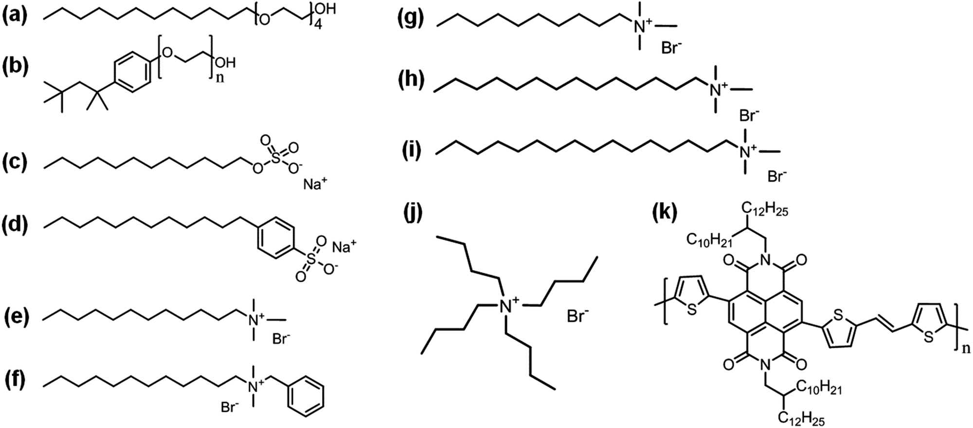
To satisfy these four essential criteria, 18 surfactants were tested to determine the universal selection rules for successful colloidization of polymer semiconductors. The surfactants studied were anionic with sulfate head groups, cationic with ammonium head groups, and non-ionic with ethoxy head groups. The molecular structures of representative surfactants are shown in Fig. 1a–j; also the other surfactants used in the experiments are listed in Fig. S1 (ESI†). As a standard polymer for colloidization tests, poly[(E)-2,7-bis(2-decyltetradecyl)-4-methyl-9-(5-(2-(5-methylthiophen-2-yl)vinyl)thiophen-2-yl)benzo[lmn][3,8]phen-anthroline-1,3,6,8(2H,7H)-tetraone] (PNDI-TVT) was selected because PNDI-TVT possesses a very planar backbone structure (Fig. 1k) and thus low solubility even in chlorinated organic solvents, making it quite difficult to fabricate colloidal particles via the miniemulsion method.18 Furthermore, there have been no research efforts to fabricate n-type water-soluble polymeric semiconductors both in terms of side chain modifications and colloid techniques.
 |
| | Fig. 1 Chemical structure of the surfactants and the n-type polymer semiconductor used in this study. (a) C12E4, (b) Triton X-100, (c) sodium dodecyl sulfate (SDS), (d) sodium dodecyl benzene sulfonate (SDBS), (e) C12-alkyl trimethyl ammonium bromide (C12TAB), (f) benzyl dodecyl ammonium bromide, (g) C10-alkyl trimethyl ammonium bromide (C10TAB), (h) C14-alkyl trimethyl ammonium bromide (C14TAB), (i) C16-alkyl trimethyl ammonium bromide (C16TAB), (j) tetrabutylammonium bromide (TBAB) and (k) poly[(E)-2,7-bis(2-decyltetradecyl)-4-methyl-9-(5-(2-(5-methylthiophen-2-yl)vinyl)thiophen-2-yl)benzo[lmn][3,8] phenanthroline-1,3,6,8(2H,7H)-tetraone] (PNDI-TVT). | |
Efficient emulsification for small and uniform particles
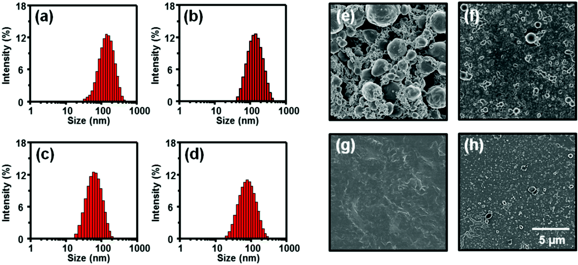
Through initial experiments, we confirmed that there are two types of surfactants that could not generate reasonably small colloidal particles via miniemulsion. Those were ionic surfactants with large aromatic hydrophobic groups (Fig. S2a–c, ESI†) and nonionic surfactants (Fig. 1a and b and Fig. S2d–f, ESI†), both of which resulted in very large particles of several hundreds of micrometers in size. All other surfactants with linear chains and charged hydrophilic groups produced stably dispersed colloidal particles. This indicates that linear alkyl tail groups of surfactants are more favorable than large aromatic tail groups, as they result in efficient van der Waals interactions with linear alkyl chains of polymer semiconductors. In addition, the failure of the miniemulsion process using non-ionic surfactants indicated that the low dispersion power of non-ionic surfactants was not enough to render small sized particles of PNDI-TVT as it has a very strong tendency for intermolecular aggregation. This is in contrast to our previous study, where non-ionic surfactants showed reasonably good dispersion ability for diketopyrrolopyrrole (DPP), a polymer with a relatively lower backbone planarity than PNDI-TVT.18 As a result, we selected four surfactants capable of efficient emulsification. Two anionic surfactants, sodium dodecyl sulfate (SDS) and sodium dodecyl benzene sulfonate (SDBS), and two cationic surfactants, dodecyl trimethyl ammonium bromide (C12TAB) and benzyl dimethyl dodecyl ammonium bromide (BDAB), were tested as shown in Fig. 1c–f. As shown in Table 1, because the critical micelle concentration and hydrophile–lipophile balance (HLB) values of each surfactant are quite different, the optimized mini-emulsion conditions were also different in terms of reaction time and solute concentration for each surfactant. Details of miniemulsion procedures can be found in the Methods section. The resulting hydrodynamic diameter and polydispersity index (PDI) of colloidal particles fabricated from these four surfactants were analyzed by means of dynamic light scattering (DLS) as summarized in Fig. 2a–d. For DLS analyses, all colloidal solutions were measured in dilute solution. The hydrodynamic diameter (nm)/PDI values of SDS-, SDBS-, C12TAB-, and BDAB-based colloidal particles were measured to be 157/0.449, 109/0.407, 70/0.615 and 92/0.527, respectively. Therefore, all four surfactants are good candidates because of the relatively small particle size as well as the narrow size distribution of the resulting colloidal solution.
Table 1 Summary of physical characteristics of various surfactants used in this work together with their corresponding measured PFET parameters cast from colloid solutions of PNDI-TVT. The statistical data were obtained from 8 independent devices for each colloid-based PFET
| Surfactants |
HLB |
Surfactant contents (mg ml−1) |
V
th (V) |
Mobility (cm2 V−1 s−1) |
On/off ratio |
| Average |
Max |
| SDS |
40 |
20 |
15 ± 8 |
0.001 ± 0.00027 |
0.0013 |
1 × 10³ |
| SDBS |
31 |
12 |
−1 ± 12 |
0.0019 ± 0.0017 |
0.0041 |
1 × 10³ |
| C12TAB |
9.3 |
4 |
3 ± 0.5 |
0.038 ± 0.0034 |
0.043 |
1 × 10³ |
| BDAB |
9.0 |
6 |
1 ± 3 |
0.017 ± 0.0066 |
0.026 |
1 × 10³ |
| C10TAB |
10.2 |
5 |
4 ± 2 |
0.020 ± 0.0043 |
0.026 |
4 × 10³ |
| C14TAB |
8.3 |
6 |
4 ± 2 |
0.037 ± 0.0051 |
0.043 |
3 × 10² |
| C16TAB |
7.4 |
5 |
2 ± 6 |
0.071 ± 0.022 |
0.10 |
8 × 10³ |
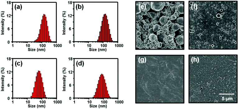 |
| | Fig. 2 (a–d) Size distributions for SDS-, SDBS-, C12TAB- and BDAB-based colloids of PNDI-TVT in a dilute solution measured by a dynamic light scattering method. (e–h) The SEM images of SDS-, SDBS-, C12TAB- and BDAB-based colloidal films deposited by spray coating. | |
Efficient coalescence of particles for high quality thin films
Nonetheless, thin film morphologies cast from SDS-, SDBS-, C12TAB-, and BDAB-based colloidal solutions were quite different as seen from the scanning electron microscopy (SEM) images in Fig. 2e–h. All the films were fabricated using a spray coating method on a SiO2 substrate modified by an octyltrichlorosilane (OTS) self-assembled monolayer. While the SDS-based colloidal films exhibited non-continuous films consisting of large localized clusters with high roughness, the C12TAB-based colloidal films exhibited smooth and continuous film morphologies. In the cases of SDBS- and BDAB-based colloidal films, continuous but very rough morphologies were observed together with some clusters. It is known that fine and smooth thin film morphologies can be achieved from colloidal solutions when interparticle coalescence phenomena occur very homogeneously throughout the entire solution–substrate interface area.23 For such an efficient and homogeneous coalescence, excess amounts of surfactant micelles should be avoided because they can cause unnecessary depletion forces between polymer particles and thus interparticle flocculation, leading to the formation of large clusters before the coalescence phenomenon. The depletion contact energy between two spherical particles can be calculated usingwhere Uc is the contact energy, n is micelle concentration, k is the Boltzmann constant, T is temperature, σ1 is the micelle diameter, and σ2 is the particle diameter. We assumed that the micelle diameters of all surfactants were 4 nm because ionic surfactants form micelles of similar size.20,24–26 The calculated Uc values of SDS, SDBS, C12TAB and BDAB were 1.24 kT, 0.47 kT, 0.18 kT, and 0.31 kT, respectively. Therefore, the non-continuous and rough morphology of SDS-based colloidal films can be attributed to the large amount of excess surfactant micelles. At the same time, the smooth and featureless morphology of the C12TAB-based colloidal film can be related to homogeneous coalescence behavior driven by a small amount of surfactant micelles. The amounts of surfactants used in experiments are listed in Table 1. It can be said that C12TAB-based colloids satisfy criteria 1 and 2 because of the formation of well-distributed and small particles as well as a minimum amount of excess surfactant. However, we wish to note that SDBS- and BDAB-based colloids also more-or-less satisfy criteria 1 and 2, although the overall quality was worse compared to C12TAB-based colloids.
Efficient removal of residual surfactants
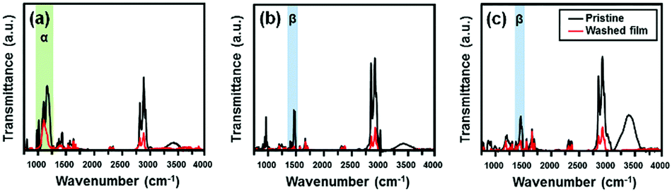
To further test criterion 3, the efficiency of surfactant removal, we conducted Fourier transform infrared (FT-IR) analyses for SDBS-, C12TAB- and BDAB-based colloidal films before and after ethanol washing as summarized in Fig. 3a–c, respectively. The absorption peaks assigned as α and β correspond to S![[double bond, length as m-dash]](https://www.rsc.org/images/entities/char_e001.gif) O and C–N stretching vibrations, respectively, which can be regarded as a characteristic feature of sulfonate and ammonium functional groups. The α peak intensities of SDBS-based colloidal films decreased by ∼50% as a result of the post-washing process, with large amounts of surfactants remaining. In the case of C12TAB- and BDAB-based colloidal films, the β peak intensities of the C12TAB-based films almost disappeared, while those of the BDAB-based films were reduced by ∼30%. These differences occur because C12TAB has the highest solubility in ethanol among the three surfactants. Collectively, we can conclude that C12TAB-based colloidal films satisfies both criteria 1 and 2 of fine film quality and criterion 3 of surfactant removal.
O and C–N stretching vibrations, respectively, which can be regarded as a characteristic feature of sulfonate and ammonium functional groups. The α peak intensities of SDBS-based colloidal films decreased by ∼50% as a result of the post-washing process, with large amounts of surfactants remaining. In the case of C12TAB- and BDAB-based colloidal films, the β peak intensities of the C12TAB-based films almost disappeared, while those of the BDAB-based films were reduced by ∼30%. These differences occur because C12TAB has the highest solubility in ethanol among the three surfactants. Collectively, we can conclude that C12TAB-based colloidal films satisfies both criteria 1 and 2 of fine film quality and criterion 3 of surfactant removal.
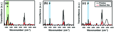 |
| | Fig. 3 FT-IR spectra of various colloid-based films before and after post-treatment for washing: (a) SDBS-, (b) C12TAB- and (c) BDAB-based colloidal films of PNDI-TVT. In each spectrum, the α (1000–1270 cm−1) region corresponds to the stretching vibration of SO in sulfonate; the β (1320–1500 cm−1) region corresponds to the stretching vibration of C–N. For comparison, the FT-IR spectrum for the dichlorobenzene-based film for the same semiconductor is shown in Fig. S3 (ESI†). | |
Efficient molecular packing of the semiconducting polymer within the colloid
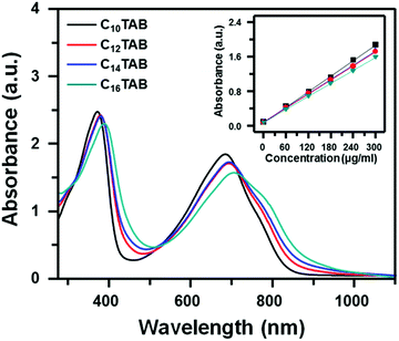
Although it was found that cationic surfactants with ammonium head groups were superior for generating polymer semiconductor colloids, further screening was required because the hydrophobic tail group of the surfactant can strongly affect both particle size and the molecular packing behavior of polymer semiconductors during the miniemulsion process. Therefore, the effect of alkyl chain length within n-alkyl trimethyl ammonium bromide (n = 10, 14 and 16) on the particle size was studied by DLS as summarized in Fig. S4a–c (ESI†). The hydrodynamic diameter gradually increased when longer alkyl chain-based surfactants were used for miniemulsion giving micelles of 77, 85, and 99 nm diameters for C10TAB, C14TAB, and C16TAB, respectively. However, because even the biggest particle size obtained from C16TAB was still ∼100 nm, all the surfactants exhibited reasonably smooth film morphologies without meaningful differences, as confirmed by the SEM images shown in Fig. S4d–f (ESI†). To ensure that all these n-alkyl trimethyl ammonium bromides satisfy criterion 3, FT-IR analyses were conducted for their corresponding colloidal films. Similar to the case of C12TAB-based colloidal films, all these colloidal films also showed very efficient surfactant removal efficiency as a result of ethanol dipping (Fig. S5a–c, ESI†). The effect of the alkyl chain length on the molecular packing of polymer semiconductors within the colloidal particles was further analyzed with UV-Vis absorption spectra as summarized in Fig. 4. Their absorption spectra were measured from colloidal solutions of C10TAB, C12TAB, C14TAB and C16TAB prepared using the same PNDI-TVT content. The inset is a plot of peak absorbance of band I (500–850 nm) near 700 nm versus the concentration of PNDI-TVT for each surfactant-based colloidal solution. Clearly observed linearity indicates that all colloidal solutions follow the Beer–Lambert law at low concentrations of 0–300 μg ml−1, indicating that all colloidal solutions behave ideally without physical interactions between water-borne colloidal particles. Therefore, we can assume that the UV-Vis absorption spectra measured at 300 μg ml−1 only reflect intra- and intermolecular charge-transfer within the polymer particle, without interparticle interactions. All the colloidal solutions showed the typical dual band absorption spectra of PNDI-TVT. The broad band I represents the typical intramolecular charge-transfer absorption resulting from the donor–acceptor structures of the polymers, and the sharp band II (300–450 nm) is assigned to be π–π* transitions. Furthermore, distinct shoulder features were also observed near 790 nm that are related to the vibronic modes of the excited electronic state. Notably, in the sequence of increasing alkyl chain length (C10TAB, C12TAB, C14TAB and C16TAB) more pronounced shoulder features can be observed. As a result, C16TAB-based colloidal solutions had the most red-shifted band maxima and pronounced vibronic features, indicating a mostly close-packed molecular structure.27 This phenomenon can be attributed to the better chemical/thermodynamic environment for molecular assembly given by surfactants with longer alkyl chains. It is well known that introducing a hydrophobic surface interlayer onto the substrate can induce enhanced self-assembly behaviour of upper-deposited polymer semiconductors, presumably due to stronger hydrophobic interaction between the alkyl chains of polymers and the surface interlayers. In particular, Rosu et al. showed that a similar mechanism can be realized in a P3HT-surfactant miniemulsion system.22 They induced a highly aligned nanostructure of the P3HT using the hydrophobic moiety of hydrophobin in an aqueous phase. In this context, we speculate that the more hydrophobic nature of surfactants with longer alkyl chains induced better intermolecular packing of polymer semiconductors, leading to the most highly-packed molecular structure in the case of the C16TAB-colloid.
 |
| | Fig. 4 UV-Vis absorption spectra of C10TAB-, C12TAB-, C14TAB- and C16TAB-based colloids of PNDI-TVT in diluted aqueous solution. (Inset: The absorption maxima of band I at ∼700 nm versus concentration of PNDI-TVT in the colloid solution plot.) | |
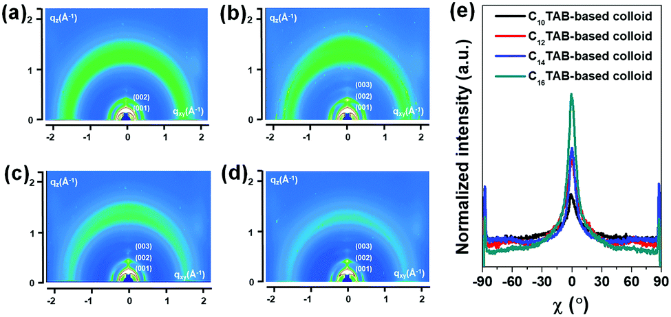
To quantitatively analyze the crystalline packing and orientation of PNDI-TVT films fabricated from C16TAB-based colloidal solutions, two-dimensional grazing incidence X-ray diffraction (2D-GIXD) analyses were conducted and compared to the case of films cast from C10TAB, C12TAB, and C14TAB-based colloids. The dichlorobenzene-based films revealed typical long-range ordering in lamellar packing structures with well-developed out-of-plane Bragg diffraction peaks up to (005) as well as pronounced π–π stacking features along the qxy direction (Fig. S6, ESI†).
As shown in Fig. 5a–d, in the case of C10TAB, C12TAB, C14TAB and C16TAB-based colloids, more spread diffraction patterns were observed from both the out-of-plane and in-plane directions, indicating less oriented molecular packing than dichlorobenzene-based films. In order to obtain more quantitative information about the crystalline orientation of the four colloid-based films, we conducted pole figure analyses as presented in Fig. 5e. For the pole figure analyses, we analyzed the distribution of the (002) orientations of four films to avoid the reflected beam. As noted, it was found that all colloid-based films still preferred the edge-on orientation. Furthermore, the degree of edge-on orientations of all the films increased with the increasing surfactant alkyl chain length. These results suggest that the molecular packing nature of polymer semiconductors in films cast from colloidal solutions are strongly affected by the original molecular packing density within the colloidal particles. In other words, the charge transport characteristics within the colloid-based films can be controlled by adjusting the molecular packing density of the polymer semiconductors within the colloidal particles.
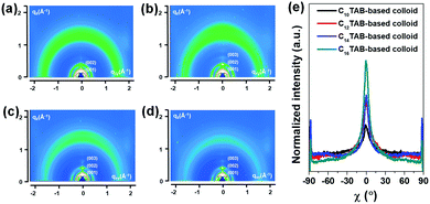 |
| | Fig. 5 GIXD images of colloid-based films cast from (a) C10TAB-, (b) C12TAB-, (c) C14TAB- and (d) C16TAB-based colloidal solutions of PNDI-TVT. For comparison, the GIXD image for the dichlorobenzene-based film is shown in Fig. S5 (ESI†). (e) The pole figures are extracted from the (002) out-of-plane Bragg diffraction peaks for each film. | |
To elucidate whether the observed molecular packing is related to charge transport characteristics, PFETs were fabricated using active layers made from PNDI-TVT films cast from C10TAB, C12TAB, C14TAB and C16TAB-based colloids. All PFETs were fabricated by spray coating the aqueous polymer colloids onto a Si/SiO2 substrate treated with octyltrichlorosilane as a top contact/bottom gate structure. All the PNDI-TVT films cast from colloidal solutions showed reasonably good n-type transfer characteristics as highlighted in Fig. S7a (ESI†). Clearly following the tendency of molecular packing analyzed from photophysical studies, the on-current and the slope of the transfer curves increased in the sequence of C10TAB, C12TAB, C14TAB and C16TAB. In the case of C16TAB, a high electron mobility of 0.1 cm2 V−1 s−1 was obtained. This is the first report of high electron mobility from polymer semiconductors processed with water. And also, the electron mobility is also comparable to PFETs fabricated using PNDI-TVT, which is completely dissolved in organic solvents, as shown in Fig. S7b (ESI†). In Fig. S8 (ESI†), we also summarized transfer characteristics of SDS-, SDBS and BDAB-based colloid PFETs, all of which showed far lower on-current and thus lower charge carrier mobility than the cases of n-alkyl trimethyl ammonium bromide (Table 1).
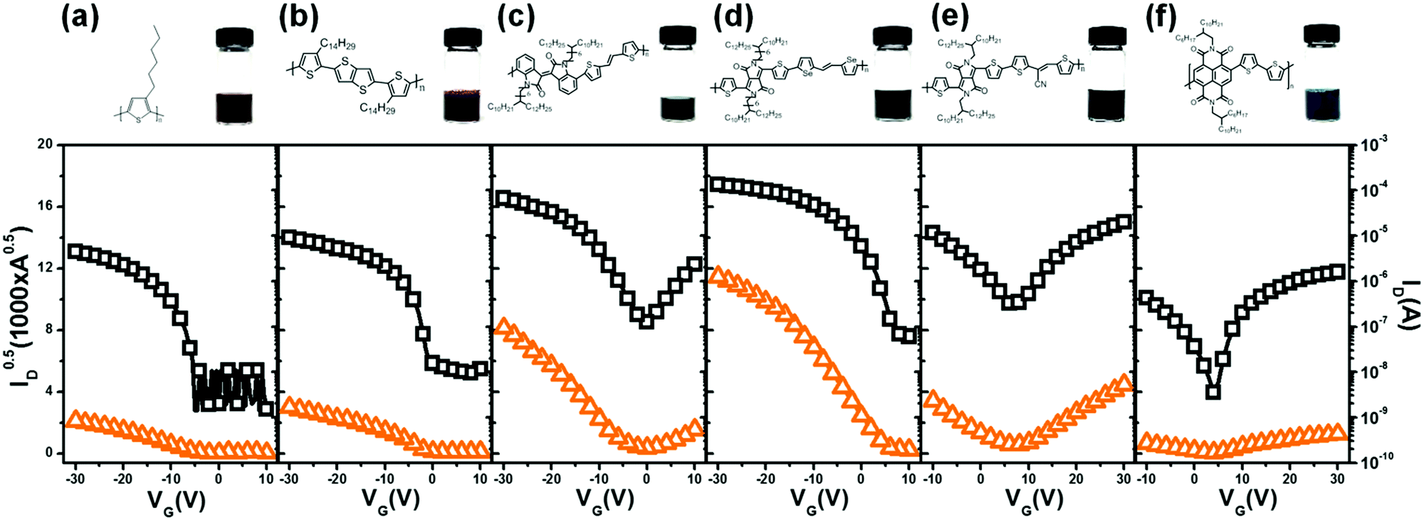
Therefore, we can argue that C16TAB satisfies all four critical criteria for the efficient fabrication of polymer semiconductor colloids for electronic application. In fact, ammonium-based cationic surfactants consisting of large enough saturated alkyl chains without an aromatic ring closely satisfy the above-mentioned key-criteria. For example, TBAB (Fig. 1k) also rendered fine film morphology with reasonably good molecular packing nature but with a slightly lower charge carrier mobility of 0.07 cm2 V−1 s−1 (Fig. S9, ESI†). As a final step, in order to confirm that the suggested universal selection rule can be applied to the miniemulsion of various polymer semiconductors, representative p-type and n-type polymers were employed for C16TAB-based colloid fabrication. These include the p-type polymers, poly(3-hexylthiophene-2,5-diyl) (P3HT), poly[2,5-bis(3-tetradecylthiophen-2-yl)thieno[3,2-b]thiophene] (PBTTT), poly[6,6′-dibromo-(N,N′-2-decylnonadecyl)-isoindigo-(E)-1,2-di(selenophen-2-yl)ethene] (PIID-SVS),28 and poly-[2,5-bis(2-decyltetradecyl)pyrrolo[3,4-c]pyrrole-1,4-(2H,5H)-dione-(E)-1,2-bis(5-(thiophen-2-yl)selenophen-2-yl)ethene] (PDPP-SVS),5 the ambipolar polymer poly[2,5-bis(2-decyltetradecyl)pyrrolo[3,4-c]pyrrole-1,4(2H,5H)-dione-(E)-[2,2′-bithiophen]-5-yl-3-(thiophen-2-yl)acrylonitrile] (PDPP-CN-TVT),29 and the n-type polymer poly((N,N′-bis(2-octyldodecyl)-1,4,5,8-naphthalenedicarboximide-2,6-diyl)-alt-5,5′-(2,2′-bithiophene)) (PNDI2OD-T2). The resulting thin films were introduced as active layers of PFET devices. All the transfer characteristics are summarized in Fig. 6. The chemical structures and the digital camera image of each colloidal solution are shown in the upper panel of Fig. 6. In addition, transfer characteristics measured from their corresponding organic solvent-based PFETs are also summarized in Fig. S10a–f (ESI†). The calculated threshold voltage, charge carrier mobility and on/off ratio of all PFETs including those prepared from colloids and organic solvents, are summarized in Table 2. Notably, colloid-based PFETs showed more than half the charge carrier mobility of PFETs processed with organic solvents, regardless of the polarity of polymer semiconductors. This level of charge carrier mobility is apparently higher than all existing studies that measure the mobility of aqueous colloids of polymer semiconductors. Interestingly, the C16TAB-based colloid technique enabled a high charge carrier mobility of 2.7 cm2 V−1 s−1 in the case of PDPP-SVS, which is higher compared to the previous study where a non-ionic surfactant was employed, revealing the overall superiority of C16TAB. In addition, we could observe that the charge carrier mobilities of PDPP-SVS and PIID-SVS, both with donor–acceptor copolymer nature as well as high emulsification efficiency, were very close to their organic solvent counterparts with relative mobilities of 64% and 69%, respectively.17
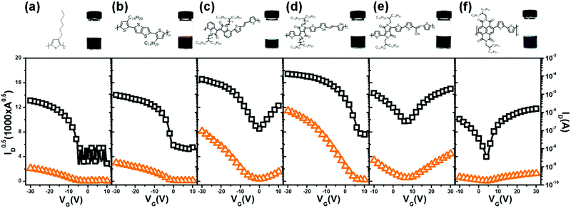 |
| | Fig. 6 Transfer characteristics of colloid-based PFETs measured under saturation conditions using p-type polymers (a–d): (a) P3HT, (b) PBTTT, (c) PIID-SVS, (d) PDPP-SVS, ambipolar polymers: (e) PDPP-CN-TVT and n-type polymers: (f) PNDI2OD-T2. For p-type, ambipolar and n-type measurements, VDS = −30 V, VDS = −30 V and VDS = 30 V were applied, respectively. | |
Table 2 Summary of all PFET parameters fabricated from various colloids and organic solvents. The statistical data were obtained from 8 independent devices
| Polymers |
Solvents |
V
th (V) |
Average mobility (cm2 V−1 s−1) |
Highest mobility (cm2 V−1 s−1) |
On/off ratio |
| Hole |
Electron |
Hole |
Electron |
| P3HT |
Water |
−5 ± 9 |
0.024 ± 0.0048 |
|
0.030 |
|
3 × 10³ |
| PBTTT |
Water |
0 ± 0.1 |
0.070 ± 0.018 |
|
0.091 |
|
1 × 10³ |
| PIID-SVS |
Water |
0 ± 0.2 |
0.90 ± 0.062 |
|
0.99 |
|
1 × 10³ |
| PDPP-SVS |
Water |
5 ± 4 |
2.4 ± 0.21 |
|
2.7 |
|
4 × 10³ |
| PDPP-CN-TVT |
Water |
7 ± 6 |
0.071 ± 0.0033 |
0.14 ± 0.030 |
0.076 |
0.18 |
1 × 10² |
| PNDI2OD-T2 |
Water |
5 ± 5 |
|
0.016 ± 0.0059 |
|
0.023 |
9× 10² |
| P3HT |
Chlorobenzene |
0 ± 0.1 |
0.060 ± 0.015 |
|
0.079 |
|
7 × 10³ |
| PBTTT |
Dichlorobenzene |
5 ± 0.1 |
0.12 ± 0.10 |
|
0.13 |
|
3 × 10³ |
| PIID-SVS |
Chloroform |
5 ± 0.1 |
1.3 ± 0.031 |
|
1.7 |
|
8 × 10³ |
| PDPP-SVS |
Chloroform |
5 ± 0.1 |
3.7 ± 0.34 |
|
4.1 |
|
2 × 10⁴ |
| PDPP-CN-TVT |
Chloroform |
5 ± 4 |
0.20 ± 0.026 |
0.57 ± 0.047 |
0.23 |
0.63 |
1 × 10² |
| PNDI2OD-T2 |
Dichlorobenzene |
2 ± 0.5 |
|
0.023 ± 0.074 |
|
0.031 |
4× 10³ |
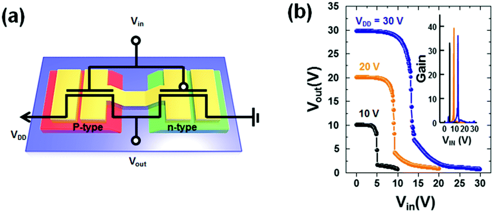
In order to emphasize the superior characteristics of C16TAB which can be universally applied to various polymer semiconductors regardless of their polarity, we fabricated a complementary inverter using water-processing for the first time. To fabricate the complementary inverter, a patterned active layer was fabricated using two colloidal solutions made from PBTTT as the p-type polymer semiconductor and PNDI-TVT as the n-type polymer semiconductor via spray coating, having symmetrical electrical characteristics to a unipolar PFET. After this, source and drain electrodes were directly deposited onto the patterned active layer by vacuum evaporation.
The device structure of the completed complementary inverter is presented in Fig. 7a. The water-processed complementary inverter exhibited very narrow transition zones, over an operating voltage range of 10 to 30 V, as shown in Fig. 7b. The threshold voltage was measured to be 4.9, 9.3, and 13.3 V, at supply voltages of 10, 20, and 30 V, respectively, which is close to half the supply voltage. The average gain of the maximum values extracted from voltage transfer characteristics with supply voltages of 10, 20, and 30 V was well above 35, and also the highest calculated gain was 40 at a supply voltage of 20 V.
 |
| | Fig. 7 (a) Schematic device structure of a complementary inverter using a C16TAB-based colloid of PBTTT and PNDI-TVT, and (b) switching characteristics of a complementary inverter. The inset shows the gain of the inverter as calculated from the switching characteristics. | |
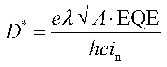
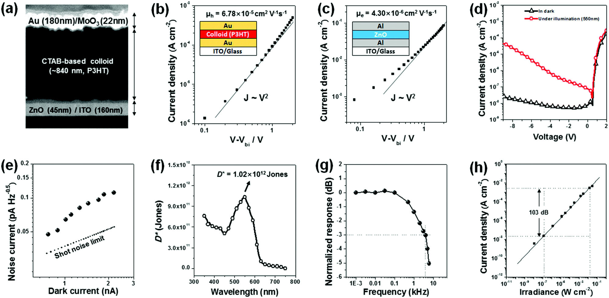
These results show that the universal colloid technique developed in this study can be applied to more complex polymeric optoelectronic devices in an environmentally friendly way, which can greatly increase the commercial value of the polymer semiconductor material. Therefore, to confirm whether the colloids of polymer semiconductors optimized by the universal selection rule can be applied to a multi-stacked optoelectronic device, we fabricated a planar heterojunction photodiode using the C16TAB-based colloid of P3HT. Fig. 8a shows the cross-sectional SEM image of a planar heterojunction photodiode with a stacking sequence of ITO/ZnO/P3HT/MoO3/Au for inverted photodiode operation. Here, the P3HT layer was prepared from a water-borne colloid technique that satisfied the universal selection rule developed in this study. The colloid of P3HT was concentrated by centrifugation using UFC500324 Amicon Ultra Centrifugal Filters for a film of suitable thickness (∼840 nm). The layers with thicknesses of 45 nm (ZnO) and 840 nm (P3HT) were determined to minimize the transit time spread of the hole/electron and also to reduce the dark current.30 The hole and electron mobilities extracted from each hole-only device of P3HT-colloid and electron-only device of ZnO were 4.30 × 10⁻⁶ cm2 V−1 s−1 and 6.78 × 10⁻⁵ cm2 V−1 s−1, respectively, as measured by the space charge limited current method, leading to well-balanced transit times of holes and electrons of 14 and 12 μs (Fig. 8b and c). The dark and illuminated J–V plot of the optimized photodiode is given in Fig. 8d. The photodiode achieved a low dark current of about 24 nA cm−2 at −9 V, comparable to high-performance polymeric photodiodes made from organic solvents.31–34 This can be attributed to smooth and compact film morphology of the active layer deposited from the C16TAB-based colloid of P3HT, as shown in Fig. 8a. Fig. 8e shows the relationship between the noise current and the dark current of the optimized PHJ photodiode. The measured noise current was found to be slightly higher than the shot noise limit. The specific detectivity (D*) was calculated to compare the performance of solvent-based photodiodes, which is given by
| |  | (2) |
e is the elementary charge,
λ is the illumination wavelength,
A is the area of the active layer, EQE is the external quantum efficiency,
h is Planck's constant,
c is the speed of light, and
in is the noise current level.
Fig. 8f shows the calculated
D* spectrum under the bias of −9 V, with the peak value of 1.02 × 10
12 Jones.
 |
| | Fig. 8 (a) A cross-section SEM image of the optimized colloid-based photodiode; the J–V characteristics for SCLC fitting of the (b) colloid-based P3HT and (c) sol–gel-based ZnO layer, respectively. The insets show the device geometries for hole-only and electron-only devices, respectively. (d) The J–V characteristics of the colloid-based photodiode (P3HT) in the dark and under illumination (at 550 nm and 120.9 μW cm−2), (e) the measured noise current at 30 Hz under various bias with theoretical shot noise limit, and (f) the calculated specific detectivity (D*) as a function of wavelength at −9 V. (g) The Bode plot under blue light illumination of 31.4 mW cm−2. The 3 dB point and 3 dB frequency point are specified with the dashed lines. (h) Linear dynamic range (LDR) for the colloid-based photodiode at −9 V. | |
Fig. 8g shows the photodiode's dynamic responses under increasing modulation frequencies of light illumination. The 3 dB bandwidth of the colloid-based diode was measured using an oscilloscope using a programmed light pulse (wavelength = 520 nm). The measured 3 dB bandwidth was 3.98 kHz, which is sufficiently fast for imaging applications.35 Also, the linear dynamic range (LDR) was measured by recording the photocurrent at −9 V, with varied light intensities from 10−2 W cm−2 to 10−7 W cm−2, and the corresponding result is shown in Fig. 8h. As a result, the responsivities of the diodes were kept constant in the low light intensity region due to the low noise current level of the photodiode. The measured LDR of 103 dB is especially notable as it is comparable to inorganic photodetectors, such as GaN (100 dB) and InGaAs (132 dB). All specific measurement methods are listed in the ESI.†![[thin space (1/6-em)]](https://www.rsc.org/images/entities/char_2009.gif) 35
35
Conclusions
Although water-borne colloid fabrication techniques have been carried out for the eco-friendly processing of polymer semiconductors, they have been limited to specific polymers and specific surfactants, and have not been applied to n-type polymer materials that are vulnerable to oxidation because of their low electron affinity. In this study, our aim was to develop a colloid fabrication technique that could be universally applied to polymer semiconductors regardless of their polarity and molecular structure. To achieve this, we set four key criteria that needed to be met by our system: (1) efficient emulsification during the miniemulsion process, (2) minimization of depletion forces, (3) high efficiency of residual surfactant removal, and (4) highly ordered self-alignment of the polymer within the particles. We tested 18 kinds of cationic, anionic and nonionic surfactants in the mini-emulsion of PNDI-TVT, an n-type semiconductor, and systematically analyzed whether the surfactant under study met the four criteria. First, we found a surfactant capable of successful emulsification for preparing small and uniform colloidal particles that coalesce homogeneously. Second, we found that the amount of surfactant used should be minimized because surfactant micelles can cause significant depletion forces between polymer particles, leading to localized clusters and non-continuous film morphologies. Third, we found that in order to improve the removal efficiency of the surfactant, a surfactant having high solubility in ethanol should be selected. Finally, we found that to realize a more compact molecular packing within the colloidal particle, a surfactant with as long an alkyl chain as possible should be selected. As a result, we developed a universal colloid technique which satisfied all the criteria and based on this technique, we fabricated high performing p-type, n-type and ambipolar water-borne PFETs, complementary inverters and photodiodes. This universal colloid technique enables the environmentally friendly manufacture of a wide variety of polymer-based optoelectronic devices, which can contribute significantly to the commercial application of polymeric semiconductor materials.
Experimental section
Experimental details and specific measurement methods of photodiodes are described in the ESI.†
Characterization
The SEM and FT-IR measurements were carefully performed after discussion with J. Park in CCRF of DGIST. The GIXD measurements were performed using the PLS-II 3C, 9A U-SAXS beamline at the Pohang Accelerator Laboratory (PAL) in Korea. The details of characterization are described in the ESI.†
Conflicts of interest
There are no conflicts to declare.
Acknowledgements
This research was supported by the National Research Foundation of Korea (NRF) Grant funded by the Ministry of Education (NRF-2015R1C1A1A02037219) and the Korea government (MSIP) (NRF-2015R1A2A1A10055620).
References
- H. Yan, Z. Chen, Y. Zheng, C. Newman, J. R. Quinn, F. Dötz, M. Kastler and A. Facchetti, Nature, 2009, 457, 679–687 CrossRef CAS PubMed.
- H. Sirringhaus, T. Kawase, R. H. Friend, T. Shimoda, M. Inbasekaran, W. Wu and E. P. Woo, Science, 2000, 290, 2123–2126 CrossRef CAS PubMed.
- Y. H. Kim, C. Sachse, M. L. Machala, C. May, L. Müller-Meskamp and K. Leo, Adv. Funct. Mater., 2011, 21, 1076–1081 CrossRef CAS.
- S. B. Darling and F. You, RSC Adv., 2013, 3, 17633–17648 RSC.
- I. Kang, H.-J. Yun, D. S. Chung, S.-K. Kwon and Y.-H. Kim, J. Am. Chem. Soc., 2013, 135, 14896–14899 CrossRef CAS PubMed.
- H. H. Choi, J. Y. Baek, E. Song, B. Kang, K. Cho, S.-K. Kwon and Y.-H. Kim, Adv. Mater., 2015, 27, 3626–3631 CrossRef CAS PubMed.
- G. Kim, S.-J. Kang, G. K. Dutta, Y.-K. Han, T. J. Shin, Y.-Y. Noh and C. Yang, J. Am. Chem. Soc., 2014, 136, 9477–9483 CrossRef CAS PubMed.
- P. G. Jessop, Green Chem., 2011, 13, 1391–1398 RSC.
- M. Shao, Y. He, K. Hong, C. M. Rouleau, D. B. Geohegan and K. Xiao, Polym. Chem., 2013, 4, 5270–5274 RSC.
- S. Gärtner, M. Christmann, S. Sankaran, H. Röhm, E.-M. Prinz, F. Penth, A. Pütz, A. E. Türeli, B. Penth, B. Baumstümmler and A. Colsmann, Adv. Mater., 2014, 26, 6653–6657 CrossRef PubMed.
- F. D. Maria, A. Zanelli, A. Liscio, A. Kovtun, E. Salatelli, R. Mazzaro, V. Morandi, G. Beramini, A. Shaffer and S. Rozen, ACS Nano, 2017, 11, 1991–1999 CrossRef PubMed.
- K. H. Cheon, H. Ahn, J. Cho, H.-J. Yun, B. T. Lim, D. J. Yun, H.-K. Lee, S.-K. Kwon, Y.-H. Kim and D. S. Chung, Adv. Funct. Mater., 2015, 25, 4844–4850 CrossRef CAS.
- L. Wang, R. Fernández-Terán, L. Zhang, D. L. A. Fernandes, L. Tian, H. Chen and H. Tian, Angew. Chem., 2016, 128, 12494–12498 CrossRef.
- K. Landfester, R. Montenegro, U. Scherf, R. Güntner, U. Asawapirom, S. Patil, D. Neher and T. Kietzke, Adv. Mater., 2002, 14, 651–655 CrossRef CAS.
- J. E. Millstone, D. F. J. Kavulak, C. H. Woo, T. W. Holcombe, E. J. Westling, A. L. Briseno, M. F. Toney and J. M. J. Fréchet, Langmuir, 2010, 26(16), 13056–13061 CrossRef CAS PubMed.
- E. B. L. Pedersen, M. C. Pedersen, S. B. Simonsen, R. G. Brandt, A. P. L. Böttiger, T. R. Andersen, W. Jiang, Z. Y. Xie, F. C. Krebs, L. Arleth and J. W. Andreasen, J. Mater. Chem. A, 2015, 3, 17022–17031 CAS.
- J. Cho, K. H. Cheon, H. Ahn, K. H. Park, S.-K. Kwon, Y.-H. Kim and D. S. Chung, Adv. Mater., 2015, 27, 5587–5592 CrossRef CAS PubMed.
- R. Kim, P. S. K. Amegadze, I. Kang, H.-J. Yun, Y.-Y. Noh, S.-K. Kwon and Y.-H. Kim, Adv. Funct. Mater., 2013, 23, 5719–5727 CrossRef CAS.
- M. Shimizu, S. Fujii, T. Tanaka and H. Kataura, J. Phys. Chem. C, 2013, 117, 11744–11749 CAS.
- F. Leal-Calderon, B. Gerhardi, A. Espert, F. Brossard, V. Alard, J. F. Tranchant, T. Stora and J. Bibette, Langmuir, 1996, 12, 872–874 CrossRef CAS.
- J.-M. Bonard, T. Stora, J.-P. Salvetat, F. Maier, T. Stöckli, C. Duschl, F. Lászó, W. A. de Heer and A. Chbtelain, Adv. Mater., 1997, 9, 827–831 CrossRef CAS.
- C. Rosu, N. Kleinhenz, D. Choi, C. J. Tassone, X. Zhang, J. O. Park, M. Srinivasarao, P. S. Russo and E. Reichmanis, Chem. Mater., 2016, 28, 573–582 CrossRef CAS.
- W. Sun, Phys. Chem. Chem. Phys., 2014, 16, 5846–5854 RSC.
- A. Dolan, R. Atkin and G. G. Warr, Chem. Sci., 2015, 6, 6189–6198 RSC.
- F. Palazzesi, M. Calvaresi and F. Zerbetto, Soft Matter, 2011, 7, 9148–9156 RSC.
- R. K. Mahajan, D. Nandni, P. A. Hassan and V. K. Aswal, Colloids Surf., A, 2011, 386, 1–10 CrossRef CAS.
- I. Cho, S. K. Park, B. Kang, J. W. Chung, J. H. Kim, K. Cho and S. Y. Park, Adv. Funct. Mater., 2016, 26, 2966–2973 CrossRef CAS.
- K. H. Park, K. H. Cheon, Y.-J. Lee, D. S. Chung, S.-K. Kwon and Y.-H. Kim, Chem. Commun., 2015, 51, 8120–8122 RSC.
- H.-J. Yun, S.-J. Kang, Y. Xu, S. O. Kim, Y.-H. Kim, Y.-Y. Noh and S.-K. Kwon, Adv. Mater., 2014, 26, 7300–7307 CrossRef CAS PubMed.
- S. Barth, P. Müller, H. Riel, P. F. Seidler, W. Rieβ, H. Vestweber and H. Bässler, J. Appl. Phys., 2001, 89, 3711–3719 CrossRef CAS.
- R. Dong, C. Bi, Q. Dong, F. Guo, Y. Yuan, Y. Fang, Z. Xiao and J. Huang, Adv. Opt. Mater., 2014, 2, 549–554 CrossRef CAS.
- G. Azzellino, A. Grimoldi, M. Binda, M. Caironi, D. Natali and M. Sampietro, Adv. Mater., 2013, 25, 6829–6833 CrossRef CAS PubMed.
- S. Wu, B. Xiao, B. Zhao, Z. He, H. Wu and Y. Cao, Small, 2016, 12, 3374–3380 CrossRef CAS PubMed.
- R. Nie, X. Deng, L. Feng, G. Hu, Y. Wang, G. Yu and J. Xu, Small, 2017, 13, 1603260 CrossRef PubMed.
- S. Yoon, J. Ha, J. Cho and D. S. Chung, Adv. Opt. Mater., 2016, 4(12), 1933–1938 CrossRef CAS.
Footnote |
| † Electronic supplementary information (ESI) available: Experimental details and specific measurement methods of the photodiode. See DOI: 10.1039/c7ee01943b |
|
| This journal is © The Royal Society of Chemistry 2017 |
Click here to see how this site uses Cookies. View our privacy policy here. 
 *d and
Dae Sung
Chung
*d and
Dae Sung
Chung